CN1155257C - Mobile detecting circuit, and noise inhibiting circuit contg. same - Google Patents
Mobile detecting circuit, and noise inhibiting circuit contg. same Download PDFInfo
- Publication number
- CN1155257C CN1155257C CNB991210085A CN99121008A CN1155257C CN 1155257 C CN1155257 C CN 1155257C CN B991210085 A CNB991210085 A CN B991210085A CN 99121008 A CN99121008 A CN 99121008A CN 1155257 C CN1155257 C CN 1155257C
- Authority
- CN
- China
- Prior art keywords
- signal
- circuit
- pixel
- edge
- polarity
- Prior art date
- Legal status (The legal status is an assumption and is not a legal conclusion. Google has not performed a legal analysis and makes no representation as to the accuracy of the status listed.)
- Expired - Fee Related
Links
Images


Classifications
-
- G—PHYSICS
- G06—COMPUTING; CALCULATING OR COUNTING
- G06T—IMAGE DATA PROCESSING OR GENERATION, IN GENERAL
- G06T7/00—Image analysis
- G06T7/20—Analysis of motion
- G06T7/246—Analysis of motion using feature-based methods, e.g. the tracking of corners or segments
Abstract
In a motion detection circuit, a difference signal between the video and one-frame delayed video signals is generated Edge signals are generated from the video and delayed video signals. Motion in a target pixel is judged from the interframe difference signal according to the edge signals. A motion judging circuit further includes an LPF and a selector for supplying an output of the LPF or the difference signal. The motion judging circuit includes a polarity deviation detecting circuit for judging the motion as moving in the presence of agreement of the polarities of all pixels at any of peripheral areas around the target pixel. The size of the peripheral areas are controlled. The motion judging circuit may further includes a peripheral pixel comparing circuit (may be bypassed) for detecting motion at the pixel by checking polarities of the difference signal at an area around the target pixel and a majority detection circuit (may be bypassed) for detecting a majority of the results of the polarity deviation detection circuit to judge the motion with deviation to a side of stopping. The polarity deviation circuit may compensate the result of the peripheral pixel comparing circuit. Width of the edge signals are controlled. A noise suppression apparatus including a motion detection circuit mentioned above is also disclosed.
Description
Technical field
The present invention relates to detect vision signal moving detecting circuit that moves and the noise suppression circuit that comprises moving detecting circuit.
Background technology
The moving detecting circuit that moves that detects in the vision signal according to the difference signal between the vision signal of a vision signal and a frame delay is that people are known, and noise suppression circuit also is known.Noise suppression circuit comprises that moving detecting circuit, the cycle signal that produces cycle signal according to difference signal and mobile detection signal produce circuit, and from vision signal, deduct cycle signal (circular signal) thus export the subtracter of a vision signal through having suppressed noise.A kind of like this moving detecting circuit of prior art and the noise suppression circuit of prior art are seen a day patent application document 9-81754 of the present disclosure.
Fig. 9 is a kind of like this block diagram of noise suppression circuit of the moving detecting circuit that includes prior art.
The moving detecting circuit of prior art comprises: from the frame memory 610 of the vision signal that through the vision signal Vo of noise suppressed, produce to postpone, produce between the vision signal of vision signal Vi and delay difference signal (frame difference signal) thus subtracter 602, move according to the video signal detection of vision signal Vi and delay and to export a moving detecting circuit 603 that moves detection signal.
Noise suppression circuit also comprises: produce the difference signal between the vision signal of vision signal Vi and delay subtracter 607, from difference signal, produces the quantitative circuit 608 of circulation of cycle signal according to mobile detection signal, thereby and obtain difference between vision signal Vi and cycle signal and export vision signal V through noise suppressed
p Subtracter 609.
Summary of the invention
The purpose of this invention is to provide a kind of superior moving detecting circuit and superior noise suppression circuit.
Comprise according to first kind of moving detecting circuit provided by the present invention: the delayer of the vision signal that postpones from video signal generating, the vision signal of delay from video signal delay a frame; The difference signal generation circuit of the frame difference signal between the vision signal of generation vision signal and delay; From the video signal detection edge of vision signal and delay and produce the edge detection signal generation circuit of edge detection signal; And, judge the mobile decision circuitry that move and export mobile detection signal in vision signal from the frame difference signal at target pixel according to edge detection signal.
First kind of moving detecting circuit also comprises: the frame difference signal is carried out the low pass filter of low-pass filtering and according to selecting signal to provide low pass filter output or the frame difference signal selector as the frame difference signal to mobile decision circuitry.
In second kind of moving detecting circuit, the mobile decision circuitry of mentioning in first kind of moving detecting circuit can comprise a polarity offset detection circuit, be used for detecting the polarity of the pixel place frame difference signal of each vision signal, be used for detecting the top left region of target pixel, the right regions of target pixel, the polarity of all pixels in any one zone of the zone, lower-left of target pixel and the lower right area of target pixel, and moving in the target pixel place judgment frame differences signal that when consistent (agreement) occurring, will move, top left region, right regions, each zone in zone, lower-left and the lower right area comprises the pixel of M * N vision signal, and M and N are natural numbers.At this moment, top left region, right regions, zone, lower-left and lower right area comprise the outside and the adjacent image point of target pixel or this target pixel.
In the third moving detecting circuit, the mobile decision circuitry of mentioning in second kind of moving detecting circuit can also comprise: peripheral pixel comparison circuit, be used for each pixel place at the presumptive area place around the target pixel, detect the polarity of frame difference signal, be used for detecting the number of presumptive area place frame difference signal positive polarity and the number of presumptive area place frame difference signal negative polarity, be used for just obtaining, the difference of negative polarity number and the absolute value of this difference, be used for the reference value that this absolute value is different with first and second relatively with output expression motion, intermediary movements or the comparative result that stops, wherein, when comparative result is represented intermediary movements, the polarity offset detection circuit is changed into comparative result according to consistency and stopping by intermediary movements, exporting mobile detection signal, and output has the mobile detection signal of constant comparative result when comparative result is represented to move and stopped.
In the third moving detecting circuit, mobile decision circuitry also comprises another polarity offset detection circuit, be used for detecting the consistency of all pixel polarity in any one zone in polarity, the top left region that detects each target pixel, right regions, zone, lower-left and the lower right area of pixel place differential signal of each vision signal, and when consistency occurring, judge moving in the target pixel place frame difference signal that will move; And a switch, be used for providing the output of polarity offset detection circuit or another polarity offset detection circuit, to export mobile detection signal according to switch controlling signal.
In the 4th kind of moving detecting circuit, the mobile decision circuitry of mentioning in second kind of moving detecting circuit also comprises: peripheral pixel comparison circuit, be used for detecting the polarity of each the pixel place frame difference signal in the presumptive area around the target pixel, detect the number of each pixel place frame difference signal positive polarity in the presumptive area and the number of interior each the pixel place frame difference signal negative polarity of presumptive area, just obtain, the difference of negative polarity number and the absolute value of this difference, this absolute value and J-1 reference value are compared, first result with output J-value, when judging that this absolute value is J median in the value, the polarity offset detection circuit changes first result for stopping according to consistency, to export second result, and mobile decision circuitry also comprises most testing circuits, it comprises a memory, this circuit is used for detecting target pixel Q second result's of Q pixel place polarity offset detection circuit great majority on every side, and judge moving in the target pixel place frame difference signal by having the great majority that are displaced to the detection that stops a side, to export mobile detection signal.
In the 5th kind of moving detecting circuit, the edge detection signal generation circuit of mentioning in first moving detecting circuit also comprises first edge detect circuit that detects the edge of vision signal, second edge detect circuit that detects the edge of the vision signal that postpones, and the 3rd edge detect circuit that detects the vision signal of vision signal edge and delay, in response to the switch of the output of selecting signal to be used for to export first, second or the 3rd edge detect circuit as edge detection signal.
In the 5th kind of moving detecting circuit, edge detection signal generation circuit is also in response to the width control signal of the value of expression m and n, and edge detection signal generation electric circuit inspection horizontal width is (2m+1) individual pixel, vertically width is the edge detection signal of (2n+1) individual pixel, here, n and m are positive integers.
In second kind of moving detecting circuit, the value of M * N is controlled according to edge detection signal.
The 4th kind of moving detecting circuit also comprises a switch in response to edge detection signal, is used for exporting according to edge detection signal the judged result of most testing circuits, or from second result of polarity offset detection circuit.
In the 4th kind of moving detecting circuit, edge detection signal generation circuit comprises first edge detect circuit, be used for detecting the edge of the vision signal of vision signal and delay, to produce first margin signal (Edgm), this signal has first pixel width that is provided to the polarity offset detection circuit, in order to the value according to first margin signal control M * N; Edge detection signal generation circuit also comprises one second edge detect circuit, edge in order to the vision signal that detects vision signal and delay, to produce second margin signal (Edgs), this second margin signal has second pixel width that is provided to most testing circuits, and the value of the value of first pixel width and second pixel width is inequality.
A kind of Noise Suppression Device that also provides according to the present invention comprises: moving detecting circuit, it comprises: delayer, in order to from vision signal, producing a delayed vision signal, delayed vision signal and video signal delay a frame; The frame difference signal generating circuit is in order to the frame difference signal of the vision signal interframe that produces vision signal and delay; Low pass filter is used for the frame difference signal is carried out low-pass filtering; Switch is used for selecting signal to export the output or the frame difference signal of low pass filter according to one; Edge detection signal generation circuit is used for detecting the edge of the vision signal of vision signal and delay, and produces an edge detection signal; And, mobile decision circuitry, according to edge detection signal, judgement is from moving in the target pixel of the vision signal of the output of switch; Cycle signal generation circuit, it comprises: coefficient generation circuit, be used for producing coefficient k according to mobile decision circuitry, here, k≤0<1; And multiplier is used for vision signal and coefficient k are multiplied each other, with the output cycle signal; And difference signal generation circuit, be used for producing the difference signal of cycle signal and vision signal interframe, with the vision signal of output through noise suppressed, wherein, moving detecting circuit can be replaced by above-mentioned each moving detecting circuit.
Description of drawings
After in conjunction with the accompanying drawings the present invention having been carried out detailed description, purpose of the present invention and feature will become and know more.Wherein,
Fig. 1 is the block diagram of one embodiment of the invention, and it provides moving detecting circuit and comprises the noise suppression circuit of this moving detecting circuit;
Fig. 2 is the block diagram of the embodiment of mobile decision circuitry structure described in Fig. 1;
That Fig. 3 describes is the embodiment of peripheral pixel comparison circuit operation among Fig. 2;
What Fig. 4 A to 4E and Fig. 5 A to 5E described is the operation of polarity offset detection circuit shown in Figure 2 among this embodiment;
What Fig. 6 described is the operation of most testing circuits among Fig. 2 among this embodiment;
Fig. 7 is a block diagram of describing edge detection signal generation circuit structure shown in Figure 1 among this embodiment;
Fig. 8 is the block diagram of modification of the present invention; And
Fig. 9 is the block diagram of noise suppression circuit of prior art that includes the moving detecting circuit of prior art.
In the accompanying drawing, identical or corresponding element or parts are represented with identical label.
Embodiment
Embodiments of the invention are described below.
Fig. 1 is the block diagram of embodiments of the invention, and it has provided moving detecting circuit and has included the structure of the noise suppression circuit of this moving detecting circuit.
The moving detecting circuit of this embodiment comprises delayer 111, and it comprises frame memory, is used for producing from vision signal Vi the vision signal that postpones; Difference signal between the vision signal Vf of generation vision signal Vi and delay is as the subtracter 102 of frame difference signal Sd; And mobile detection signal generation circuit 103, be used for detecting moving among the frame difference signal Sd of target pixel place, to export mobile detection signal Sm.
Noise suppression circuit also comprise from vision signal Vi and delayed vision signal Vf produce frame difference signal Sd subtracter 108, produce the cycle signal generation circuit 109 of cycle signal according to mobile detection signal Sm from the frame difference signal, and obtain difference between vision signal Vi and cycle signal with the subtracter 110 of output through the vision signal Vo of noise suppressed.
Cycle signal generation circuit 109 comprises: according to the coefficient generation circuit 113 that produces coefficient k from the mobile detection signal Sm of mobile decision circuitry 107, k≤0<1 here; And the multiplier 114 that vision signal and this coefficient k are multiplied each other.
Subtracter 102 or 108 can save.If only adopt moving detecting circuit, the input to delayer 111 provides vision signal Vi so, rather than through the vision signal Vo of noise suppressed.Delayer 111 makes vision signal Vi postpone the frame of this vision signal Vi.
To be provided to subtracter 102, subtracter 108 and subtracter 110 at the vision signal Vi of video signal input terminal 101 places input.Subtracter 110 deducts cycle signal Sm from vision signal Vi, be the vision signal of noise suppressed of the output of noise suppression circuit with generation.Be provided to delayer 111 through the vision signal Vo of noise suppressed, it comprises frame memory, makes frame of video signal delay, and exports delayed vision signal Vf.Subtracter 102 deducts delayed vision signal Vf from vision signal Vi, be provided to the frame difference signal of the selector 105 of low pass filter 104 and mobile detection signal generation circuit 103 with generation.Frame difference signal Sd carries out low-pass filtering by low pass filter 104.Selector 105 is according to selecting signal 112 to select the output of frame difference signal or low pass filter 104.Promptly, the switching of selector 105 is that the frequecy characteristic according to the frame difference signal Sd that is provided to mobile detection signal generation circuit 103 carries out, in order to the frame difference signal for the following optimum frequency feature that mobile decision circuitry 107 has that will mention to be provided.
Mobile detection signal generation circuit 103 also comprises the edge detection signal generation circuit 106 that detects vision signal Vi and delayed video signal Vf and produce edge detection signal Edgm and Edgs, and judges mobile in the target pixel frame difference signal and export the mobile decision circuitry 107 of mobile detection signal Sm from the output of selector 105 according to edge detection signal Edgm and Edgs.
Edge detection signal generation circuit 106 detects the marginal portion of target from the vision signal Vf of vision signal Vi and delay, with the edge detection signal Edgm of polarization offset detection circuit 202 and the edge detection signal of most testing circuit 205.Mobile decision circuitry 107 is judged the mobile degree at target pixel TP place, and the result is provided to cycle signal generation circuit 109.
On the other hand, subtracter 108 produces frame difference signal Sd, and this frame difference signal Sd is sent to cycle signal generation circuit 109, definite COEFFICIENT K below being resembled by this cycle signal generation circuit 109:
When moving when mobile K=k3 among the frame difference signal Sd that judges the target pixel place.
When moving to middle when mobile K=k2 among the frame difference signal Sd that judges the target pixel place.
When moving when stopping K=k1 among the frame difference signal Sd that judges the target pixel place.0≤k3<k2<k1<1。
With multiplier 114 frame difference signal Sd be multiply by COEFFICIENT K, be provided to the cycle signal of subtracter 110 with generation.Subtracter 110 deducts cycle signal from vision signal Vi, to produce the vision signal Vo through noise suppressed as described above.
Fig. 2 is the block diagram of this embodiment, and it has provided the structure of the mobile decision circuitry 107 shown in Fig. 1.
Mobile decision circuitry 107 comprises peripheral pixel comparison circuit 201, polarity offset compensation circuit 206 and most testing circuit 203.
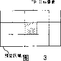
What Fig. 3 described is the operation of the peripheral pixel comparison circuit 201 of this embodiment.
Peripheral pixel comparison circuit 201 as shown in Figure 3, detect around the target pixel polarity of each frame difference signal Sd of pixel place in the presumptive area (for example comprise target pixel TP 5 * 3), the number of the negative polarity NP of frame difference signal in the number of the positive polarity PP of frame difference signal Sd and the presumptive area in the detection presumptive area, just obtain, poor (PP-PN) of negative polarity number and the absolute value of difference | PP-PN|, with absolute value | the reference value that PP-PN| is different with first and second (J-1 different reference value) is relatively, promptly, TH_S and TH_M are to export first judged result (J value result).
When TH_M≤| during PP-NP|, the vision signal at target pixel place is judged as mobile (Smo).
When TH_S≤| during PP-NP|<TH_M, move (Smi) in the middle of the vision signal at target pixel place is judged as.
When 0≤| during PP-NP|<TH_S, the vision signal at target pixel place is judged as stops (Sst).
First judged result of J-value (three-value) is provided to the judged result that moves according to the centre and implements to move the polarity offset detection circuit of judging 202 once more.J is the natural number greater than 1.
What Fig. 4 A to 4E and Fig. 5 A to 5E described is will be by the pixel area of polarity offset detection circuit 202 processing.Lower right area LR shown in lower-left area L L shown in right regions UR shown in top left region UL shown in Fig. 4 B, Fig. 4 C, Fig. 4 D and Fig. 4 E comprises the target pixel shown in Fig. 4 A.On the other hand, the lower right area shown in the zone, lower-left shown in the right regions shown in the top left region shown in Fig. 5 B, Fig. 5 C, Fig. 5 D and Fig. 5 E is in the outside of the target pixel TP shown in Fig. 5 A, but close target pixel TP.
Polarity offset compensation circuit 206 comprises polarity offset detection circuit 202 and inverter 207,208 and " or (OR) " doors 209 of " with (AND) " door.According to the mobile Smi as a result in the centre of peripheral pixel comparison circuit 201, the consistency of the polarity of all pixels in any one zone among the lower right area LR of the right regions UR of the polarity of differential signal (differential signal) Sd of polarity offset detection circuit 202 each pixel of detection vision signal, the top left region UL that detects target pixel, target pixel, the lower-left area L L of target pixel and target pixel, and when unanimity occurring, judge that moving in the target pixel TP place frame difference signal is motion.
When peripheral pixel comparison circuit 201 is judged moving to middle when moving (Smi) of target pixel TP places, the polarity skew with inverter 207 and with door 208, move first judged result that (Smi) compensates peripheral pixel comparison circuit 201 from the centre.On the other hand, or door 209 results according to polarity offset detection circuit 202, the judged result of the peripheral pixel comparison circuit 201 of uncompensation.
More particularly, when peripheral pixel comparison circuit 201 judges that moving is middle moving, and the polarity offset detection circuit judges that moving is motion, then peripheral offset detection circuit 202 is in signal Sst place output L logic level, in signal Smi place output H logic level (with the output of door 208), be L logic level (or output of door 209) at signal Smo place.According to signal Smi, polarity offset detection circuit 202 judges and moves, and if second judged result is to stop, polarity offset detection circuit 202 output H logic levels then.Then, inverter 207 output L logic levels, thus change into the L logic level with the H logic level of output place of door 208.On the other hand, or the L logic level of door 209 output place constant.
If second judged result of polarity offset detection circuit 202 is not motion, so, polarity offset detection circuit 202 output L logic levels, thus keep the H logic levels with door 208, and or the output of door 209 keep the L logic level.As mentioned above, move judgement once more, thereby more accurate judgement is provided.
In addition, second judged result is provided to most testing circuits 203, judges, thereby provide again further accurate moving to judge to provide further to move.
What Fig. 6 described is the operation of most testing circuits 203 among this embodiment.
Most testing circuits 203 comprise a memory 204 that is used for storing second judged result of polarity offset compensation circuit 206, read and output comprises second judged result in the predetermined outer peripheral areas of the pixel of Q shown in Fig. 6 (for example target pixel TP around 8 pixels), most testing circuits 203 also comprise most detectors 205 and switch S 1.Most detectors 205 detect target pixel Q result's of Q pixel place polarity offset compensation circuit 206 great majority on every side.Switch S 1 is exported the result of most detectors 205 or second judged result of polarity offset compensation circuit 206 according to edge detection signal Edgs, to export mobile detection signal Sm.
Most detectors 205 detect the majority of 8 second judged results, if and provide identical judged result more than R1 pixel, then most detectors 205 detect most as the 3rd judged result, so that the judged result of the adjacent image point around the mobile judgement at target pixel TP place and the target pixel TP equates, to avoid mutual incoherent judged result.More particularly, if the mobile of 4 pixel places in 8 adjacent image points is judged as motion, and move in the middle of mobile being judged as at 4 pixel places in addition, then the 3rd judged result moves in the middle of being.If move in the middle of 4 adjacent image point places mobile is judged as being, and mobile being judged as being at 4 pixel places stops in addition, and it is to stop that the 3rd judged result of target pixel is judged as, and is weighted to the 3rd judged result that stops side to provide.That is, the centre that peripheral pixel comparison circuit 201 is judged is moved the motion of judging with polarity offset detection circuit 202 and is judged as once more and stops, thereby has reduced to be in the noise at the image place of halted state.
Fig. 7 is the structured flowchart of the edge detection signal generation circuit 106 of this embodiment shown in Fig. 1.
Edge detection signal generation circuit 106 comprises the first edge detect circuit 301a, the second edge detect circuit 301b or door 304 or door 305 and edge selection circuit 302.According to width control signal 308, the first edge detect circuit 301a detects the edge of vision signal Vi, its transverse width is (2m+1) individual pixel (target pixel, with m right pixel and m left pixel), vertically width is (2n+1) individual pixel (target pixel and n top pixel and n bottom pixel), to produce edge detection signal Edgmi, and the edge of detection vision signal Vi, the transverse width of vision signal Vi is (2m+1)+q pixel, vertically width is (2n+1)+r pixel, to produce edge detection signal Edgsi.According to width control signal 308, the second edge detect circuit 301b detects the edge of vision signal Vf, its transverse width is (2m+1) individual pixel, vertically width is (2n+1) individual pixel, with generation edge detection signal Edgmf, and the edge of detection vision signal Vf, its transverse width is (2m+1)+q pixel, and vertically width is (2n+1)+r pixel, to produce edge detection signal Edgsf.
Or the edge detection signal of door 304 generations between edge detection signal Edgmi and Edgmf.Or the edge detection signal of door 305 generations between edge detection signal Edgsi and Edgsf.According to selecting signal 303, circuit 302 output edge detection signal Edgmi, edge detection signal Edgmf are selected in the edge, or as edge detection signal Edgm's or door 304 output, and output edge detection signal Edgsi, edge detection signal Edgsf, or as edge detection signal Edgs's or door 305 output.
Edge detection signal Edgm and Edgs representative have the edge of H logic level (1) and have the open and flat part of L logic level (0).
Polarity detection circuit 202 is according to edge detection signal Edgm, and the size of control top left region UL, right regions UR, lower-left area L L and lower right area LR (M, N).More particularly, when edge detection signal is H (1), and the pixel in this zone (M, number N) reduces, for example, be 3 * 2 pixels, and, if edge detection signal is L (0), (number of M * N) is for bigger then to make pixel, for example be 5 * 2 pixels, thus being suppressed of afterimage, and the noise in the stop area reduces.
Similarly, the edge detection signal Edgs that is used for most testing circuits 204 starts or forbids most detectors 205.More particularly, when the edge detection signal Edgs that is used for most testing circuits 204 is H (1), switch S 1 is from polarity offset compensation circuit 206 outputs second judged result, perhaps from most detectors 205 outputs the 3rd judged results, thereby the final judged result that prevents to illustrate the target pixel place at edge is judged as being once more towards stopping side.More particularly, according to edge detection signal Edgs, switch S 1 or from second judged result of polarity offset compensation circuit 206 export target pixel TP, perhaps from most detectors 205 outputs the 3rd judged results.
As mentioned above, mobile detection is implemented more accurately, move the afterimage that causes by image and be suppressed thereby make, and the noise that stops part being inhibited.
Fig. 8 is the amended block diagram of the present invention.
Modification shown in Fig. 8 is identical with the embodiment shown in Fig. 1 substantially.Difference is, also is equipped with another polarity offset detection circuit 210 and switch S 2.According to switch controlling signal, switch S 2 outputs are from second judged result of polarity offset compensation circuit 206, perhaps from polarity offset detection circuit 210 output judged results.When mobile, polarity offset compensation circuit 206 compensates in the middle of first judged result of peripheral pixel comparison circuit is.On the other hand, the polarity consistency of all pixels in the lower right area LR of the lower-left area L L of the right regions UR of the top left region UL of target pixel, target pixel, target pixel and target pixel among polarity offset detection circuit 210 each target pixel TP of detection, and when unanimity occurring, judge moving among the frame difference signal Sd in the target pixel TP to moving.When switch controlling signal was represented a side of polarity offset detection circuit 210, switch S 2 provided the judged result of being made by polarity offset detection circuit 210.
Claims (26)
1. moving detecting circuit, it comprises:
Deferred mount, its uses delay circuit delays to be input to the vision signal of described moving detecting circuit, producing delayed vision signal, described delayed vision signal than described video signal delay a frame;
The frame difference signal generation apparatus is used for producing the frame difference signal between described vision signal and described delayed vision signal;
The edge detection signal generating means is used for detecting the edge of the vision signal of described vision signal and described delay, and produces an edge detection signal; And
Movement judging device is used for according to described edge detection signal, judges in the target pixel place from described frame difference signal and states moving the vision signal, to export mobile detection signal.
2. moving detecting circuit as claimed in claim 1 is characterized in that it also comprises:
Described frame difference signal is carried out the low pass filter of low-pass filtering; And
Be provided to the selector of described movement judging device according to output or the described frame difference signal of selecting signal with described low pass filter as described frame difference signal.
3. moving detecting circuit as claimed in claim 1, it is characterized in that, described movement judging device comprises the polarity offset detection circuit, the polarity of frame difference signal is stated in each the pixel place that is used for detecting described vision signal, detect the top left region of described target pixel, the right regions of described target pixel, the consistency of the polarity of all pixels in any one zone in the zone, lower-left of described target pixel and the lower right area of described target pixel, and when consistency occurring, judge that it is motion that moving in the frame difference signal stated in described target pixel place, described top left region, described right regions, zone, described lower-left and described lower right area comprise M * N pixel of described vision signal respectively, here, M and N are natural numbers.
4. moving detecting circuit as claimed in claim 3 is characterized in that, described top left region, described right regions, zone, described lower-left and described lower right area comprise described target pixel.
5. moving detecting circuit as claimed in claim 3 is characterized in that, described top left region, described right regions, zone, described lower-left and described lower right area are in the outside of described target pixel, and close described target pixel.
6. moving detecting circuit as claimed in claim 3 is characterized in that, described movement judging device also comprises:
Peripheral pixel comparison circuit, be used for detecting around the described target pixel each pixel place in the presumptive area and state the polarity of frame difference signal, detect the number of the positive polarity of described frame difference signal in the described presumptive area and the number that the negative polarity of frame difference signal is stated in interior each the pixel place of described presumptive area, obtain just described, the number difference of negative polarity and the absolute value of described difference, the reference value that described absolute value is different with first and second relatively, with output expression motion, middle move or stop in one comparative result, wherein represent motion and described comparative result when representing that described centre is mobile when the judgement of described polarity offset detection circuit, described polarity offset detection circuit changes described comparative result.
7. moving detecting circuit as claimed in claim 6, it is characterized in that, described movement judging device also comprises another polarity offset detection circuit, the consistency of the described polarity of all pixels in any one zone is stated in the polarity of frame difference signal, the described top left region that detects each described target pixel, described right regions, zone, described lower-left and the described lower right area in each the pixel place that is used for detecting described vision signal, and when described consistency occurring, judge that it is motion that moving in the frame difference signal stated in described target pixel place; Described movement judging device also comprises a switch, is used for according to a switch controlling signal, and the output of described polarity offset detection circuit or described another polarity offset detection circuit is provided, to export described mobile detection signal.
8. moving detecting circuit as claimed in claim 3 is characterized in that, described movement judging device also comprises:
Peripheral pixel comparison circuit, be used for detecting around the described target pixel each pixel place in the presumptive area and state the polarity of frame difference signal, detect each pixel place in the described presumptive area and state the number that the negative polarity of frame difference signal is stated in each pixel place in the number of positive polarity of frame difference signal and the described presumptive area, obtain just described, the number difference between the negative polarity and the absolute value of described difference, described absolute value and J-1 reference value are compared, first result with output J value, in J comparative result of its expression one, when described difference be judged as being the expression J comparative result J value in median the time, described polarity offset detection circuit changes described first result according to described consistency, and output is different from one second result in described first result and the expression comparative result; And described movement judging device also comprises most testing circuits, it comprises a memory, be used for detecting around the described target pixel Q pixel place and state second result's of polarity offset detection circuit great majority, and judging further that according to described detected majority described target pixel place states described move in the frame difference signal, J is the natural number greater than 1.
9. moving detecting circuit as claimed in claim 1, it is characterized in that, described edge detection signal generating means comprise the edge that detects described vision signal first edge detect circuit, detect described delay vision signal the edge second edge detect circuit, detect the 3rd edge detect circuit at edge of the vision signal of described vision signal and described delay, and in response to selecting a output in signal output described first, second and the 3rd edge detect circuit as the switch of edge detection signal.
10. moving detecting circuit as claimed in claim 9, it is characterized in that, described edge detection signal generating means is also in response to the width control signal of the value of expression m and n, it is the edge of (2n+1) individual pixel for (2m+1) individual pixel, vertical width that described edge detection signal generating means detection has horizontal width, and wherein said m and n are positive integers.
11. moving detecting circuit as claimed in claim 3 is characterized in that, the value of described M and N is controlled according to described edge detection signal.
12. moving detecting circuit as claimed in claim 8, it is characterized in that, it also comprises a switch, and described switching response is in described edge detection signal, is used for exporting according to described edge detection signal the described judged result or described second comparative result of described most testing circuits.
13. moving detecting circuit as claimed in claim 8, it is characterized in that, described edge detection signal generating means comprises first edge detect circuit, be used for detecting the edge of the vision signal of described vision signal and described delay, be provided to first margin signal with first pixel width of described polarity offset detection circuit with generation, control the value of described M * N according to described first margin signal, described edge detection signal generating means also comprises second edge detect circuit, be used for detecting the edge of the vision signal of described vision signal and described delay, be provided to second margin signal with second pixel width of described most testing circuits with generation, described first pixel width is different with described second pixel width.
14. a noise suppressor is characterized in that it comprises:
Motion detection device, it comprises:
Deferred mount, it produces delayed vision signal by delayed video signal, and the vision signal of described delay is compared with described vision signal and has been postponed a frame;
The frame difference signal generation apparatus is used for producing the frame difference signal between the vision signal of described vision signal and described delay;
Low pass filter is used for described frame difference signal is carried out low-pass filtering;
Switch is used for selecting signal to export the output or the described frame difference signal of described low pass filter according to one;
The edge detection signal generating means is used for detecting the edge of the vision signal of described vision signal and described delay, and produces edge detection signal; With
Movement judging device is used for according to described edge detection signal, states moving the vision signal in the target pixel place from the output judgement of described switch; And
The cycle signal generating means, it comprises:
The coefficient generating means is used for judged result according to described movement judging device, produces coefficient k, 0≤k<1; With
Multiplier is used for described vision signal and described coefficient k are multiplied each other, to export a cycle signal; And
The difference signal generating means is used for producing the difference signal between described cycle signal and the described vision signal, with the vision signal of output through noise suppressed.
15. noise suppressor as claimed in claim 14 is characterized in that, when described movement judging device judges that described moving is the described coefficient k that stops greater than judge the described described coefficient k that moves when moving when described movement judging device.
16. noise suppressor as claimed in claim 14, it is characterized in that, described movement judging device comprises the polarity offset detection circuit, the polarity of frame difference signal is stated in each the pixel place that is used for detecting described vision signal, detect the top left region of described target pixel, the right regions of described target pixel, the consistency of the described polarity of all pixels in any one zone in the zone, lower-left of described target pixel and the lower right area of described target pixel, and when unanimity occurring, judge that it is motion that moving in the frame difference signal stated in described target pixel place, described top left region, described right regions, in zone, described lower-left and the described lower right area each all comprises M * N pixel of described vision signal, and M and N are natural numbers.
17. noise suppressor as claimed in claim 16 is characterized in that, each in described top left region, described right regions, zone, described lower-left and the described lower right area all comprises described target pixel.
18. noise suppressor as claimed in claim 16 is characterized in that, described top left region, described right regions, zone, described lower-left and described lower right area are the outsides at described target pixel, and contiguous described target pixel.
19. noise suppressor as claimed in claim 16, it is characterized in that, described movement judging device also comprises: peripheral pixel comparison circuit, be used for detecting around the described target pixel each pixel place in the presumptive area and state the polarity of frame difference signal, detect the number of the described frame difference signal negative polarity of each pixel in the number of described frame difference signal positive polarity in the described presumptive area and the described presumptive area, obtain just described, the difference of negative polarity number and the absolute value of described difference, the reference value that described absolute value is different with first and second relatively, with output expression motion, middle move and stop in one comparative result, wherein, described polarity offset detection circuit changes described comparative result when described comparative result represents that the judgement of the mobile and described polarity offset detection circuit in described centre is represented to move.
20. noise suppressor as claimed in claim 19, it is characterized in that, described movement judging device also comprises another polarity offset detection circuit, the polarity of frame difference signal is stated in each the pixel place that is used for detecting described vision signal, detect the described top left region of each described target pixel, described right regions, the consistency of the described polarity of all pixels in any one zone in zone, described lower-left and the described lower right area, and when consistency occurring, judge that it is motion that moving in the frame difference signal stated in described target pixel place, described movement judging device also comprises a switch, be used for providing the output of described polarity offset detection circuit and described another polarity offset detection circuit, to export described mobile detection signal according to switch controlling signal.
21. noise suppressor as claimed in claim 18 is characterized in that, described movement judging device also comprises:
Peripheral pixel comparison circuit, be used for detecting around the described target pixel each pixel place in the presumptive area and state the polarity of frame difference signal, detect each pixel place in the described presumptive area and state the number that frame difference signal negative polarity is stated in each pixel place in the number of positive polarity of frame difference signal and the described presumptive area, obtain just described, the difference of negative polarity number and the absolute value of described difference, described absolute value and J-1 reference value are compared, first comparative result with J value of output, in J comparative result of its expression one, when described difference be judged as being the expression J comparative result J value in median the time, described polarity offset detection circuit changes described first result according to described consistency, and output is different from one second result in described first result and the expression comparative result; And described movement judging device also comprises most testing circuits, it comprises a memory, be used for detecting around the described target pixel Q pixel place and state second result's of polarity offset detection circuit great majority, and judging further that according to described detected majority the described of described target pixel move, J is the natural number greater than 1.
22. noise suppressor as claimed in claim 14, it is characterized in that, described edge detection signal generating means comprise the edge that detects described vision signal first edge detect circuit, detect described delay vision signal the edge second edge detect circuit, detect described vision signal and described delay vision signal the edge the 3rd edge detect circuit and select signal and export in described first, second and the 3rd edge detect circuit one output in response to one as the switch of edge detection signal.
23. noise suppressor as claimed in claim 22, it is characterized in that, described edge detection signal generating means is also in response to the width control signal of the value of expression m and n, and described edge detection signal generating means detection level width be (2m+1) individual pixel and vertically width be the described edge of (2n+1) individual pixel, wherein said n and m are positive integers.
24. noise suppressor as claimed in claim 16 is characterized in that, the value of described M * N is controlled according to described edge detection signal.
25. noise suppressor as claimed in claim 21, it is characterized in that, it also comprises a second switch, and described second switch is in response to described edge detection signal, is used for exporting according to described edge detection signal the described judged result or described second comparative result of described most testing circuits.
26. noise suppressor as claimed in claim 21, it is characterized in that, described edge detection signal generating means comprises one first edge detect circuit, be used for detecting the described edge of the vision signal of described vision signal and described delay, first margin signal that has first pixel width with generation, this first margin signal is provided to described polarity offset detection circuit, in order to control the value of described M * N according to described first margin signal, described edge detection signal generating means also comprises one second edge detect circuit, be used for detecting the described edge of the vision signal of described vision signal and described delay, second margin signal that has second pixel width with generation, this second margin signal is provided to described most testing circuit, and the value of described first pixel width is different with the value of described second pixel width.
Applications Claiming Priority (2)
| Application Number | Priority Date | Filing Date | Title |
|---|---|---|---|
| JP27625398A JP3285545B2 (en) | 1998-09-29 | 1998-09-29 | Motion detection circuit and noise reduction device |
| JP276253/1998 | 1998-09-29 |
Publications (2)
| Publication Number | Publication Date |
|---|---|
| CN1251005A CN1251005A (en) | 2000-04-19 |
| CN1155257C true CN1155257C (en) | 2004-06-23 |
Family
ID=17566856
Family Applications (1)
| Application Number | Title | Priority Date | Filing Date |
|---|---|---|---|
| CNB991210085A Expired - Fee Related CN1155257C (en) | 1998-09-29 | 1999-09-29 | Mobile detecting circuit, and noise inhibiting circuit contg. same |
Country Status (4)
| Country | Link |
|---|---|
| US (1) | US6687300B1 (en) |
| EP (1) | EP0991016A3 (en) |
| JP (1) | JP3285545B2 (en) |
| CN (1) | CN1155257C (en) |
Cited By (1)
| Publication number | Priority date | Publication date | Assignee | Title |
|---|---|---|---|---|
| CN102754422A (en) * | 2010-02-15 | 2012-10-24 | 夏普株式会社 | Motion detection device, control programme, and integrated circuit |
Families Citing this family (12)
| Publication number | Priority date | Publication date | Assignee | Title |
|---|---|---|---|---|
| US6798910B1 (en) * | 2001-05-17 | 2004-09-28 | The United States Of America As Represented By The Secretary Of The Air Force | Self-optimizing edge detection in blurred, high-noise images |
| WO2004002135A1 (en) * | 2002-06-25 | 2003-12-31 | Matsushita Electric Industrial Co., Ltd. | Motion detection device and noise reduction device using that |
| US7762665B2 (en) | 2003-03-21 | 2010-07-27 | Queen's University At Kingston | Method and apparatus for communication between humans and devices |
| WO2004084054A2 (en) * | 2003-03-21 | 2004-09-30 | Queen's University At Kingston | Method and apparatus for communication between humans and devices |
| US8292433B2 (en) | 2003-03-21 | 2012-10-23 | Queen's University At Kingston | Method and apparatus for communication between humans and devices |
| TWI401944B (en) * | 2007-06-13 | 2013-07-11 | Novatek Microelectronics Corp | Noise cancellation device for an image signal processing system |
| EP2114068A1 (en) * | 2008-04-30 | 2009-11-04 | Sony Corporation | Method for converting an image and image conversion unit |
| US8224033B2 (en) * | 2008-06-24 | 2012-07-17 | Mediatek Inc. | Movement detector and movement detection method |
| US20100295782A1 (en) | 2009-05-21 | 2010-11-25 | Yehuda Binder | System and method for control based on face ore hand gesture detection |
| JP5193976B2 (en) * | 2009-09-14 | 2013-05-08 | 日立コンシューマエレクトロニクス株式会社 | Video processing apparatus and video display apparatus |
| US8953097B2 (en) | 2011-11-15 | 2015-02-10 | Nec Corporation | Motion vector estimation device, motion vector estimation method, and program for estimating motion vector |
| WO2013147756A1 (en) * | 2012-03-28 | 2013-10-03 | Intel Corporation | Content aware selective adjusting of motion estimation |
Family Cites Families (12)
| Publication number | Priority date | Publication date | Assignee | Title |
|---|---|---|---|---|
| JPH0191586A (en) | 1987-10-02 | 1989-04-11 | Nippon Hoso Kyokai <Nhk> | Moving detection circuit |
| JP2934036B2 (en) | 1991-03-07 | 1999-08-16 | 松下電器産業株式会社 | Motion detection method and noise reduction device |
| US5428693A (en) | 1991-04-12 | 1995-06-27 | Mitsubishi Denki Kabushiki Kaisha | Motion compensation predicting coding method and apparatus |
| US5497203A (en) * | 1991-10-30 | 1996-03-05 | Mitsubishi Denki Kabushiki Kaisha | Motion detection circuit for high definition television based on muse |
| JPH05174148A (en) * | 1991-12-26 | 1993-07-13 | Sony Corp | Motion detecting circuit |
| JPH06351002A (en) * | 1993-06-08 | 1994-12-22 | Matsushita Electric Ind Co Ltd | Motion signal detecting method and video signal processor using the same |
| JPH07131676A (en) | 1993-10-28 | 1995-05-19 | Toshiba Corp | Movement detecting circuit |
| US5539469A (en) * | 1994-12-30 | 1996-07-23 | Daewoo Electronics Co., Ltd. | Apparatus for determining motion vectors through the use of an adaptive median filtering technique |
| JPH0981754A (en) | 1995-09-19 | 1997-03-28 | Matsushita Electric Ind Co Ltd | Movement detecting circuit |
| JPH09163373A (en) | 1995-12-08 | 1997-06-20 | Toshiba Corp | Noise reduction device |
| JP3240936B2 (en) * | 1996-09-30 | 2001-12-25 | 日本電気株式会社 | Motion processing circuit |
| US6061100A (en) * | 1997-09-30 | 2000-05-09 | The University Of British Columbia | Noise reduction for video signals |
-
1998
- 1998-09-29 JP JP27625398A patent/JP3285545B2/en not_active Expired - Fee Related
-
1999
- 1999-09-13 US US09/394,685 patent/US6687300B1/en not_active Expired - Fee Related
- 1999-09-28 EP EP99119275A patent/EP0991016A3/en not_active Withdrawn
- 1999-09-29 CN CNB991210085A patent/CN1155257C/en not_active Expired - Fee Related
Cited By (2)
| Publication number | Priority date | Publication date | Assignee | Title |
|---|---|---|---|---|
| CN102754422A (en) * | 2010-02-15 | 2012-10-24 | 夏普株式会社 | Motion detection device, control programme, and integrated circuit |
| CN102754422B (en) * | 2010-02-15 | 2015-03-11 | 夏普株式会社 | Motion detection device, control programme, and integrated circuit |
Also Published As
| Publication number | Publication date |
|---|---|
| EP0991016A3 (en) | 2000-10-25 |
| JP2000115585A (en) | 2000-04-21 |
| EP0991016A2 (en) | 2000-04-05 |
| CN1251005A (en) | 2000-04-19 |
| US6687300B1 (en) | 2004-02-03 |
| JP3285545B2 (en) | 2002-05-27 |
Similar Documents
| Publication | Publication Date | Title |
|---|---|---|
| CN1155257C (en) | Mobile detecting circuit, and noise inhibiting circuit contg. same | |
| CN1155225C (en) | Mobile detecting circuit and noise suppression circuit containing the same circuit | |
| CN1096184C (en) | Motion picture detecting method | |
| CN1266934C (en) | Method and device for video frequency removing interleave | |
| CN1254086C (en) | Image processor, image processing method and processing program | |
| CN1027119C (en) | Motion signal processor | |
| CN101079958A (en) | Video signal processing apparatus and image display apparatus | |
| CN1783946A (en) | Systems and methods for image processing and video player for realizing by the method | |
| CN1170421C (en) | Mobile detecting circuit and noise inhibiting circuit including said mobile detecting circuit | |
| CN1681292A (en) | Display apparatus | |
| JP2006305352A5 (en) | ||
| CN1362832A (en) | Data processing method | |
| CN1129301C (en) | Image converter and image conversion method | |
| CN1249619C (en) | Impact suppession method and device for image detail enhancment | |
| CN1193594C (en) | Signal processing device and signal processing method | |
| CN1571473A (en) | Apparatus and method for processing signal | |
| CN1237782C (en) | Deinterlaced scanning device and method | |
| CN1539119A (en) | Image processing apparatus for and method of improving image and image display apparatus comprising image processing apparatus | |
| CN1531332A (en) | Image processor, image processing method and processing program | |
| CN1508751A (en) | Photoelectric mouse and method for preventing it from anormal operation | |
| CN1862654A (en) | Display for dynamic contrast of image processing effect and display method | |
| CN1127848C (en) | Circuit for transforming an image rate | |
| CN1545812A (en) | Device and process for estimating noise level, noise reduction system and coding system comprising such a device | |
| JPH0981754A (en) | Movement detecting circuit | |
| JPH0846925A (en) | Motion detection circuit for picture signal |
Legal Events
| Date | Code | Title | Description |
|---|---|---|---|
| C10 | Entry into substantive examination | ||
| SE01 | Entry into force of request for substantive examination | ||
| C06 | Publication | ||
| PB01 | Publication | ||
| C14 | Grant of patent or utility model | ||
| GR01 | Patent grant | ||
| CF01 | Termination of patent right due to non-payment of annual fee |
Granted publication date: 20040623 Termination date: 20140929 |
|
| EXPY | Termination of patent right or utility model |