CN115513737A - Socket device, accessory socket device, and electronic device - Google Patents
Socket device, accessory socket device, and electronic device Download PDFInfo
- Publication number
- CN115513737A CN115513737A CN202210612994.7A CN202210612994A CN115513737A CN 115513737 A CN115513737 A CN 115513737A CN 202210612994 A CN202210612994 A CN 202210612994A CN 115513737 A CN115513737 A CN 115513737A
- Authority
- CN
- China
- Prior art keywords
- accessory
- camera
- contacts
- contact
- socket
- Prior art date
- Legal status (The legal status is an assumption and is not a legal conclusion. Google has not performed a legal analysis and makes no representation as to the accuracy of the status listed.)
- Pending
Links
Images


Classifications
-
- H—ELECTRICITY
- H01—ELECTRIC ELEMENTS
- H01R—ELECTRICALLY-CONDUCTIVE CONNECTIONS; STRUCTURAL ASSOCIATIONS OF A PLURALITY OF MUTUALLY-INSULATED ELECTRICAL CONNECTING ELEMENTS; COUPLING DEVICES; CURRENT COLLECTORS
- H01R33/00—Coupling devices specially adapted for supporting apparatus and having one part acting as a holder providing support and electrical connection via a counterpart which is structurally associated with the apparatus, e.g. lamp holders; Separate parts thereof
- H01R33/945—Holders with built-in electrical component
-
- H—ELECTRICITY
- H01—ELECTRIC ELEMENTS
- H01R—ELECTRICALLY-CONDUCTIVE CONNECTIONS; STRUCTURAL ASSOCIATIONS OF A PLURALITY OF MUTUALLY-INSULATED ELECTRICAL CONNECTING ELEMENTS; COUPLING DEVICES; CURRENT COLLECTORS
- H01R13/00—Details of coupling devices of the kinds covered by groups H01R12/70 or H01R24/00 - H01R33/00
- H01R13/62—Means for facilitating engagement or disengagement of coupling parts or for holding them in engagement
- H01R13/629—Additional means for facilitating engagement or disengagement of coupling parts, e.g. aligning or guiding means, levers, gas pressure electrical locking indicators, manufacturing tolerances
-
- G—PHYSICS
- G03—PHOTOGRAPHY; CINEMATOGRAPHY; ANALOGOUS TECHNIQUES USING WAVES OTHER THAN OPTICAL WAVES; ELECTROGRAPHY; HOLOGRAPHY
- G03B—APPARATUS OR ARRANGEMENTS FOR TAKING PHOTOGRAPHS OR FOR PROJECTING OR VIEWING THEM; APPARATUS OR ARRANGEMENTS EMPLOYING ANALOGOUS TECHNIQUES USING WAVES OTHER THAN OPTICAL WAVES; ACCESSORIES THEREFOR
- G03B15/00—Special procedures for taking photographs; Apparatus therefor
- G03B15/02—Illuminating scene
- G03B15/03—Combinations of cameras with lighting apparatus; Flash units
- G03B15/05—Combinations of cameras with electronic flash apparatus; Electronic flash units
-
- G—PHYSICS
- G03—PHOTOGRAPHY; CINEMATOGRAPHY; ANALOGOUS TECHNIQUES USING WAVES OTHER THAN OPTICAL WAVES; ELECTROGRAPHY; HOLOGRAPHY
- G03B—APPARATUS OR ARRANGEMENTS FOR TAKING PHOTOGRAPHS OR FOR PROJECTING OR VIEWING THEM; APPARATUS OR ARRANGEMENTS EMPLOYING ANALOGOUS TECHNIQUES USING WAVES OTHER THAN OPTICAL WAVES; ACCESSORIES THEREFOR
- G03B17/00—Details of cameras or camera bodies; Accessories therefor
- G03B17/56—Accessories
- G03B17/566—Accessory clips, holders, shoes to attach accessories to camera
-
- G—PHYSICS
- G03—PHOTOGRAPHY; CINEMATOGRAPHY; ANALOGOUS TECHNIQUES USING WAVES OTHER THAN OPTICAL WAVES; ELECTROGRAPHY; HOLOGRAPHY
- G03B—APPARATUS OR ARRANGEMENTS FOR TAKING PHOTOGRAPHS OR FOR PROJECTING OR VIEWING THEM; APPARATUS OR ARRANGEMENTS EMPLOYING ANALOGOUS TECHNIQUES USING WAVES OTHER THAN OPTICAL WAVES; ACCESSORIES THEREFOR
- G03B31/00—Associated working of cameras or projectors with sound-recording or sound-reproducing means
-
- H—ELECTRICITY
- H01—ELECTRIC ELEMENTS
- H01R—ELECTRICALLY-CONDUCTIVE CONNECTIONS; STRUCTURAL ASSOCIATIONS OF A PLURALITY OF MUTUALLY-INSULATED ELECTRICAL CONNECTING ELEMENTS; COUPLING DEVICES; CURRENT COLLECTORS
- H01R33/00—Coupling devices specially adapted for supporting apparatus and having one part acting as a holder providing support and electrical connection via a counterpart which is structurally associated with the apparatus, e.g. lamp holders; Separate parts thereof
- H01R33/97—Holders with separate means to prevent loosening of the coupling or unauthorised removal of apparatus held
-
- G—PHYSICS
- G03—PHOTOGRAPHY; CINEMATOGRAPHY; ANALOGOUS TECHNIQUES USING WAVES OTHER THAN OPTICAL WAVES; ELECTROGRAPHY; HOLOGRAPHY
- G03B—APPARATUS OR ARRANGEMENTS FOR TAKING PHOTOGRAPHS OR FOR PROJECTING OR VIEWING THEM; APPARATUS OR ARRANGEMENTS EMPLOYING ANALOGOUS TECHNIQUES USING WAVES OTHER THAN OPTICAL WAVES; ACCESSORIES THEREFOR
- G03B2215/00—Special procedures for taking photographs; Apparatus therefor
- G03B2215/05—Combinations of cameras with electronic flash units
- G03B2215/0514—Separate unit
- G03B2215/056—Connection with camera, e.g. adapter
-
- H—ELECTRICITY
- H01—ELECTRIC ELEMENTS
- H01R—ELECTRICALLY-CONDUCTIVE CONNECTIONS; STRUCTURAL ASSOCIATIONS OF A PLURALITY OF MUTUALLY-INSULATED ELECTRICAL CONNECTING ELEMENTS; COUPLING DEVICES; CURRENT COLLECTORS
- H01R13/00—Details of coupling devices of the kinds covered by groups H01R12/70 or H01R24/00 - H01R33/00
- H01R13/02—Contact members
- H01R13/22—Contacts for co-operating by abutting
- H01R13/24—Contacts for co-operating by abutting resilient; resiliently-mounted
-
- H—ELECTRICITY
- H01—ELECTRIC ELEMENTS
- H01R—ELECTRICALLY-CONDUCTIVE CONNECTIONS; STRUCTURAL ASSOCIATIONS OF A PLURALITY OF MUTUALLY-INSULATED ELECTRICAL CONNECTING ELEMENTS; COUPLING DEVICES; CURRENT COLLECTORS
- H01R13/00—Details of coupling devices of the kinds covered by groups H01R12/70 or H01R24/00 - H01R33/00
- H01R13/62—Means for facilitating engagement or disengagement of coupling parts or for holding them in engagement
- H01R13/629—Additional means for facilitating engagement or disengagement of coupling parts, e.g. aligning or guiding means, levers, gas pressure electrical locking indicators, manufacturing tolerances
- H01R13/631—Additional means for facilitating engagement or disengagement of coupling parts, e.g. aligning or guiding means, levers, gas pressure electrical locking indicators, manufacturing tolerances for engagement only
Abstract
The invention relates to a socket device, an accessory socket device and an electronic device. An accessory shoe device attachable to an electronic device in a first direction and a shoe device detachable from the accessory shoe device include: a plurality of connection terminals arranged in a second direction perpendicular to the first direction; a socket engagement portion engageable with an accessory socket device; and a terminal protection portion configured to protrude toward a front end side of the first direction with respect to the socket engagement portion and protect the plurality of connection terminals. The plurality of connection terminals are exposed in a direction perpendicular to the first direction and the second direction with respect to the terminal protection portion, and include slopes inclined in the exposure direction from an inner side to an outer side of the second direction on both sides of the second direction of the terminal protection portion.
Description
Technical Field
The present invention relates to a socket device with which an accessory is equipped so that the accessory can be attached to and detached from an electronic device, and an accessory socket device with which an electronic device is equipped.
Background
An image pickup apparatus (electronic apparatus) such as a digital camera includes an accessory shoe apparatus attachable to and detachable from a shoe apparatus of an accessory such as a lighting apparatus (flash unit). The accessory shoe device includes an engagement member engageable with the shoe device and configured to hold the shoe device, and the accessory shoe device and the shoe device each include a connection terminal for enabling bidirectional communication between the image pickup device and the accessory. Conventionally, the number of connection terminals is generally five.
Japanese patent laid-open ("JP") No. 2018-084681 discloses an electronic viewfinder having an accessory shoe apparatus attachable to and detachable from an image pickup apparatus, and the accessory shoe apparatus and the shoe apparatus maintain compatibility with conventional five connection terminals (communication pins) and increase the number of connection terminals within the shape of an engagement member.
However, if the outlet device having a large number of connection terminals as disclosed in JP 2018-084681 preferentially ensures an area required to arrange these connection terminals, an area for protecting the shapes of these communication terminals and a positioning area between components are limited. In addition, in the case where the outlet device includes a terminal protection portion for protecting the connection terminal separately from a portion engageable with the engagement member of the accessory outlet device, and an external force is applied to the accessory in a state where the terminal protection portion contacts the engagement member of the accessory outlet device alone, the terminal protection portion may be damaged.
Disclosure of Invention
The present invention provides a compact socket apparatus and the like each of which can secure an area for arranging many communication terminals, an area for protecting the shapes of the communication terminals, and a positioning area between components, and suppress damage of a terminal protecting portion.
A socket apparatus according to an aspect of the present invention is attachable to and detachable from an accessory socket apparatus of an electronic apparatus in a first direction. The outlet device includes: a plurality of connection terminals arranged in a second direction perpendicular to the first direction; a receptacle engagement portion engageable with an accessory receptacle device; and a terminal protection portion configured to protrude toward a front end side in the first direction with respect to the receptacle engagement portion, and protect the plurality of connection terminals. The plurality of connection terminals are exposed in a direction perpendicular to the first direction and the second direction with respect to the terminal protection portion, and both sides in the second direction of the terminal protection portion include slopes inclined in the exposure direction from an inner side to an outer side in the second direction.
An accessory according to another aspect of the invention includes the above-described outlet device. An accessory shoe device according to another aspect of the present invention is attachable to and detachable from the shoe device described above. An electronic device according to another aspect of the present invention includes the accessory shoe device described above.
Further features of the invention will become apparent from the following description of exemplary embodiments with reference to the attached drawings.
Drawings
Fig. 1 shows the structure of a camera and an accessory according to a first embodiment of the present invention.
Fig. 2A to 2C show an example of a camera with an accessory attached and a contact configuration thereof according to a first embodiment.
Fig. 3A and 3B illustrate how an external force is applied to an accessory attached to a camera according to the first embodiment.
Fig. 4A shows a structure for determining the connection state of the ground contact according to the first embodiment.
Fig. 4B is a flowchart illustrating processing performed by the camera according to the first embodiment.
Fig. 5A and 5B show a flowchart of processing performed by the camera according to the first embodiment.
Fig. 6A, 6B, and 6C are timing charts showing signal changes when the contact adjacent to the power supply contact is short-circuited according to the first embodiment.
Fig. 7 shows an example of assignment of function signals to accessory types according to the first embodiment.
Fig. 8A, 8B, and 8C show connection destination structures of function signals according to the first embodiment.
Fig. 9 shows a structural example of a camera and an accessory according to the first embodiment.
Fig. 10 shows another structural example of the camera and the accessory according to the first embodiment.
Fig. 11 shows still another structural example of the camera and the accessory according to the first embodiment.
Fig. 12 shows a structural example of the fitting according to the first embodiment.
Fig. 13 shows a structural example of a camera, an accessory, and an intermediate accessory according to the first embodiment.
Fig. 14 shows another structural example of the camera, the accessory, and the intermediate accessory according to the first embodiment.
Fig. 15A and 15B are timing charts in the case where the accessory is a strobe (strobe) device according to the first embodiment.
Fig. 16A, 16B, and 16C are perspective views of a camera according to the first embodiment and an external strobe unit as an accessory.
Fig. 17A and 17B are an exploded view and a perspective view of the accessory shoe according to the first embodiment.
Fig. 18A, 18B, and 18C show the configuration of the engagement member and the connection terminal connector of the accessory shoe according to the first embodiment.
Fig. 19A and 19B are a perspective view and a sectional view of an external strobe unit according to the first embodiment.
Fig. 20A, 20B, and 20C are a perspective view and a front view showing an internal configuration of the camera connector according to the first embodiment.
Fig. 21A and 21B are a top view and a sectional view of the camera connector according to the first embodiment.
Fig. 22A and 22B are a perspective view and a sectional view of an external strobe unit according to a modification.
Fig. 23A and 23B are a perspective view and a front view showing an internal configuration of a connector according to a modification.
Fig. 24 is a front view of the accessory shoe according to the first embodiment.
Fig. 25 is a partially enlarged view of the connection plug according to the first embodiment.
Fig. 26 is a front sectional view showing a state in which the camera connector according to the first embodiment is attached to the accessory shoe.
Fig. 27A and 27B are a perspective view and a sectional view of an external strobe unit according to the first embodiment.
Fig. 28A and 28B are a perspective view and a front view showing an internal configuration of the camera connector according to the first embodiment.
Fig. 29A to 29C are a perspective view and a sectional view of a digital camera and an external strobe unit according to the first embodiment.
Fig. 30 shows a top cover fitting receptacle according to the first embodiment.
Fig. 31A to 31C show a drip-proof configuration according to the first embodiment.
Fig. 32 is a front view showing a state in which the camera connector according to the second embodiment is attached to the accessory shoe.
Fig. 33 shows a perspective view of an accessory shoe according to a second embodiment.
Fig. 34A and 34B are a perspective view and a front view showing an internal configuration of a camera connector according to the second embodiment.
Fig. 35 is a front view showing a state in which the camera connector according to the second embodiment is attached to the accessory shoe.
Fig. 36A and 36B are top views of the accessory shoe and the camera connector according to the second embodiment.
Fig. 37 is a front view showing a state in which the camera connector according to the second embodiment is attached to the accessory shoe.
Fig. 38A and 38B illustrate a positional relationship between the inclined surface and the connection terminal of the camera connector according to the second embodiment.
Detailed Description
Embodiments according to the present invention will now be described with reference to the accompanying drawings.
First embodiment
Fig. 1 shows an electrical configuration of a camera 100 as an electronic apparatus and an accessory 200 detachably attached to the camera 100 according to a first embodiment of the present invention. In the camera 100 and the accessory 200, a plurality of contacts (terminals) TC01 to TC21 of a camera connector 141 provided in the camera 100 and a plurality of contacts TA01 to TA21 of an accessory connector 211 provided in the accessory 200 are connected to each other in one-to-one correspondence, respectively, whereby these contacts are electrically connected to each other.
The camera 100 is supplied with power from a battery 111. The battery 111 may be attached to the camera 100 and detached from the camera 100. A camera control circuit 101, which is a control part of the camera 100, is a circuit that controls the entire camera 100, and includes a microcomputer having a built-in CPU or the like.
The system power supply circuit 112 is a circuit that generates power for supplying power to each circuit in the camera 100, and includes a DC/DC converter circuit, an LDO (low drop out) circuit, a charge pump circuit, and the like. The 1.8V voltage generated by the system power supply circuit 112 is constantly supplied from the battery 111 to the camera control circuit 101 as a camera microcomputer power source VMCU _ C. The camera control circuit 101 controls the system power supply circuit 112, and thereby controls on and off of power supply to each circuit of the camera 100.
The optical lens 121 is attachable to the camera 100 and detachable from the camera 100. Light from a subject incident via the optical lens 121 is imaged on an image sensor 122 including a CMOS sensor or a CCD sensor or the like. The object image formed on the image sensor 122 is encoded into a digital image pickup signal. The image processing circuit 123 performs image processing such as noise reduction processing and white balance processing on the digital image pickup signal to generate image data, and converts the image data into an image file such as JPEG format to record the image data in the recording memory 126. The image processing circuit 123 generates VRAM image data for display on the display circuit 127 from the image data.
The memory control circuit 124 controls transmission and reception of image data and other data generated by the image processing circuit 123 and the like. The volatile memory 125 is a memory capable of high-speed reading and writing, such as a DDR3 SDRAM, and is used for a work space or the like of image processing by the image processing circuit 123. The recording memory 126 is a readable and writable recording medium such as an SD card or a CFexpress card that is attachable to and detachable from the camera 100 via a connector not shown. The display circuit 127 is a display located on the back surface of the camera 100, and includes an LCD panel, an organic EL display panel, and the like. The backlight circuit 128 adjusts the luminance of the display circuit 127 by changing the light amount of the backlight of the display circuit 127.
In the present embodiment, the accessory power supply circuit a131 and the accessory power supply circuit B132, which are power supply means, are each a voltage conversion circuit that converts a voltage supplied from the system power supply circuit 112 into a predetermined voltage and generates 3.3V as the accessory power supply VACC.
The accessory power supply circuit a131 is a power supply circuit including an LDO and the like and having low self-consumption power. The accessory power supply circuit B132 is a circuit including a DC/DC converter circuit and the like, and can flow a current larger than that of the accessory power supply circuit a 131. The accessory power supply circuit B132 consumes more power than the accessory power supply circuit a 131. Therefore, the accessory power supply circuit a131 is more efficient than the accessory power supply circuit B132 when the load current is small, and the accessory power supply circuit B132 is more efficient than the accessory power supply circuit a131 when the load current is large. The camera control circuit 101 controls on and off of the voltage outputs of the accessory power supply circuits a131 and B132 according to the operating state of the accessory 200.
The protection circuit 133 as a protection component includes a current fuse element, a multi-switch element, an electronic fuse circuit combining a resistor, an amplifier, and a switch element, and the like, and outputs the overcurrent detection signal DET _ OVC when the value of the power supply current from the accessory power supply circuits a131 and B132 to the accessory 200 becomes excessively large (abnormal) and exceeds a predetermined value. In the present embodiment, the protection circuit 133 includes an electronic fuse circuit, and notifies the camera control circuit 101 by the overcurrent detection signal DET _ OVC in the case where a current of 1A or more flows. The overcurrent detection signal DET _ OVC indicates an overcurrent by the Hi level.
The camera connector 141 is a connector for electrically connecting with the accessory 200 via 21 contacts TC01 to TC21 arranged in a row. The contacts TC01 to TC21 are arranged in the order of the contacts TC01 to TC21 from one end to the other end in the arrangement direction thereof.
TC01 is connected to a ground terminal (GND) and serves not only as a contact for a reference potential (GND potential) but also as a contact for controlling wiring impedances of differential signals D1N and D1P described below. TC01 corresponds to a third ground contact.
The differential signal D1N connected to TC02 and the differential signal D1P connected to TC03 are paired differential data communication signals that perform data communication, and are connected to the camera control circuit 101. TC02, TC03, TC07 to TC17, TC19, and TC20, which will be described later, are communication contacts.
TC04 as a first ground contact is connected to GND and serves as a reference potential contact between the camera 100 and the accessory 200. The TC04 is arranged outside the TC05 described below in the contact arrangement direction.
The accessory power VACC generated by the accessory power supply circuits a131 and B132 is connected to the TC05 as a power supply contact via the protection circuit 133.
The accessory attachment detection signal/ACC _ DET is connected to TC06 as an attachment detection contact. The accessory attachment detection signal/ACC _ DET is pulled up to the camera microcomputer power supply VMCU _ C via the resistor element Rp134 (10 k Ω). The camera control circuit 101 can detect whether the accessory 200 is attached by reading the signal level of the accessory attachment detection signal/ACC _ DET. The accessory 200 is detected as unattached if the signal level (potential) of the accessory attachment detection signal/ACC _ DET is Hi level (predetermined potential), and the accessory 200 is detected as attached if the signal level (potential) of the accessory attachment detection signal/ACC _ DET is Lo level (GND potential as described later).
When the camera 100 is powered on and the signal level (potential) of the accessory attachment detection signal/ACC _ DET changes from the Hi level to the Lo level, various kinds of transmission are performed between the camera 100 and the accessory 200 via the contacts.
When the attached state of the accessory 200 is detected, the camera control circuit 101 supplies power to the accessory 200 via the TC05 as a power supply contact.
SCLK connected to TC07, MOSI connected to TC08, MISO connected to TC09, and CS connected to TC10 are signals to be used by the camera control circuit 101 as a communication master for SPI (serial peripheral interface) communication. In the present embodiment, the communication clock frequency of the SPI communication is 1MHz.
A communication request signal/WAKE for requesting communication from the accessory 200 to the camera control circuit 101 is connected to the TC11. The communication request signal/WAKE is pulled up to the camera microcomputer power supply VMCU _ C via a resistor. The camera control circuit 101 may receive a communication request from the accessory 200 by detecting the trailing edge of the communication request signal/WAKE.
The SDA connected to the TC12 and the SCL connected to the TC13 are signals that the camera control circuit 101 serves as a communication master and performs I2C (inter-integrated circuit) communication. The SDA and SCL are signals for communication in an open drain manner (hereinafter referred to as open drain communication) pulled up to the camera microcomputer power supply VMCU _ C, and the communication frequency is 100kbps in the present embodiment.
In the I2C communication, both data transmission from the camera 100 and data transmission from the accessory 200 are performed via the SDA. When comparing the SPI communication and the I2C communication with each other, the communication speed of the I2C communication is lower than that of the SPI communication, and lower power consumption can be achieved. The SPI communication has a higher communication speed than the I2C communication, and is therefore suitable for communication of information having a large data amount. Therefore, in the communication between the camera 100 and the accessory 200 according to the present embodiment, information having a large data amount is communicated in the SPI communication, and information having a small data amount is communicated in the I2C communication. For example, data is first communicated in I2C communication, and control is performed such that SPI communication is further performed in a case where SPI communication can be performed or needs to be performed based on the data.
The FNC1 signal connected to TC14 (synchronization contact), the FNC2 signal connected to TC15, the FNC3 signal connected to TC16, and the FNC4 signal connected to TC17 are signals whose functions can be changed according to the type of accessory 200 attached. For example, where the accessory 200 is a microphone device, the signal communicated via the TC15 is an audio data signal. In the case where the accessory 200 is a lighting (strobe or flash) unit, the signal communicated via the TC14 is a signal for controlling the light emission timing. Depending on the type of accessory attached, signals for implementing different functions may be communicated via the same contacts. For example, in the case where the accessory 200 is an accessory other than the lighting unit, a synchronization signal for controlling timing different from light emission timing may be communicated via the TC 14. TC14 to TC17 correspond to functional signal contacts. Communication using at least one of the functional signal contacts is also referred to as functional signal communication.
The functional signal communication may be performed in parallel with the I2C communication and the SPI communication at a timing independent of the I2C communication or the SPI communication.
The type of accessory as used herein means the microphone device and the lighting unit and the like described above. Accessories that achieve the same purpose (such as lighting with different properties, etc.) are of the same type. The accessories that fulfil different purposes, such as microphone devices and lighting units, are of different types.
The function signal communication is performed based on the information acquired by the I2C communication or the SPI communication.
TC18 as a second ground contact (reference potential contact) is also connected to GND, and is a contact serving as a reference potential between the camera 100 and the accessory 200, similar to TC 04.
The differential signal D2N connected to the TC19 (first differential signal contact) and the differential signal D2P connected to the TC20 (second differential signal contact) are paired data communication signals that perform data communication and are connected to the camera control circuit 101. For example, USB communications may be conducted via TC19 and TC 20.
TC21 is connected to GND and can be used not only as a contact for reference potential but also as a contact for controlling wiring impedance of the differential signals D2N and D2P. TC21 corresponds to the fourth ground contact. The contacts TC01, TC04, TC06, TC18, and TC21 are connected to, for example, a GND part of the flexible substrate 158 shown in fig. 17A and 17B, which will be described later, and the GND part of the flexible substrate 158 is fixed to a metal member having a GND level of the camera 100 by a screw 157 or the like. The metal member having the GND level includes, for example, the bonding member 151 and a base plate, not shown, inside the camera 100.
The present embodiment arranges the attachment detection contact TC06 to which the accessory attachment detection signal/ACC _ DET is connected next to the contact (first clock Zhong Chudian) TC07 that transmits SCLK (first clock signal) as a clock signal. In general, noise (clock noise) due to potential fluctuation of a clock signal is transmitted to a contact adjacent to a contact of the clock signal, which may cause malfunction. In particular, in a structure having a large number of contacts and a short distance between the contacts as in the present embodiment, the influence is more significant. Therefore, arranging the attachment detection contact TC06 next to the SCLK contact TC07 can suppress the influence of clock noise.
The accessory attachment detection signal/ACC _ DET is pulled up before the accessory attachment, but is set to the GND potential after the accessory attachment. On the other hand, the SCLK contact TC07 that transmits the clock signal does not transmit the clock signal before the accessory attachment, and thus the potential does not fluctuate. Only after the attachment of the accessory, the potential fluctuates due to the transmission of the clock signal.
When the SCLK contact TC07 transmits a clock signal, the attachment detection contact TC06 is at the GND potential. Therefore, even if the attachment detection contact TC06 receives clock noise, the potential of the control circuit of the camera 100 or the accessory 200 is less likely to fluctuate, so that malfunction can be prevented. In addition, the transmission of clock noise to a position farther than the attachment detection contact TC06 can be suppressed. As a result, since it is not necessary to arrange the GND terminal, the influence of the clock noise can be suppressed without increasing the number of contacts.
SCL (second clock signal) as a clock signal is also sent to the contact (second clock contact) TC13. However, the frequency of SCLK transmitted to SCLK contact TC07 is higher than the frequency of SCL, and SCLK contact TC07 generates more clock noise than SCL contact TC13. Therefore, arranging the attachment detection contact TC06 next to the SCLK contact TC07 instead of next to the SCL contact TC13 can provide a greater effect of preventing malfunction due to clock noise.
In addition to the difference in frequency, SCL transmitted by SCL contact TC13 is a clock signal of the I2C communication standard, and the voltage fluctuation of the signal line is driven by the open-drain connection. On the other hand, SCLK transmitted by SCLK contact TC07 is a clock signal conforming to the SPI communication standard, and the voltage fluctuation of the signal line is driven by the CMOS output. Therefore, the edge of the voltage fluctuation of SCL contact TC13 tends to be gentler than SCLK contact TC07, and clock noise is less likely to occur. Therefore, arranging the attachment detection contact TC06 next to the SCLK contact TC07 rather than next to the SCL contact TC13 is more effective in preventing malfunction caused by clock noise.
The differential signals D1N and D1P may be transmitted to the first and second differential signal contacts TC19 and TC20 in pairs to transmit clock signals. At this time, a clock signal (third clock signal) having a higher frequency than that of SCLK contact TC07 or SCL contact TC13 may be transmitted. Since the differential signals D1N and D1P are paired signals, the transmission of clock noise is smaller than that of the SCLK contact TC07 or the SCL contact TC13 that transmits a single-ended signal. Therefore, arranging the attachment detection contact TC06 next to the SCLK contact TC07 instead of the first and second differential signal contacts TC19 and TC20 can more effectively prevent malfunction caused by clock noise.
A contact point (first data contact point) TC08 arranged on the opposite side of the SCLK contact point TC07 from the attachment detection contact point TC06 transmits MOSI (first data signal). MOSI appears to be susceptible to clock noise since it is a data signal. Since MOSI is a data signal of the same SPI communication standard as the clock signal transmitted by SCLK contact TC07, the fluctuation timing of the potential is synchronized with the clock signal and is less affected by clock noise. Therefore, the contact TC08 does not have to be fixed to the GND potential, and can be used as a MOSI contact.
The accessory 200 has a battery 205, and receives power supply from the battery 205, and also receives power supply from the camera 100 via the camera connector 141 and the accessory connector 211. An accessory control circuit 201, which is a control part of the accessory 200, is a circuit that controls the entire accessory 200, and is a microcomputer having a built-in CPU or the like.
Accessory power supply circuit 202 is a circuit that generates power to be supplied to each circuit of accessory 200, and includes a DC/DC converter circuit, an LDO, a charge pump circuit, and the like. The voltage 1.8V generated by the accessory power supply circuit 202 is constantly supplied to the accessory control circuit 201 as the accessory microcomputer power VMCU _ a. The on and off of the power supply to each circuit of the accessory 200 is controlled by controlling the accessory power supply circuit 202.
The charging circuit 204 is a circuit for charging the battery 205 using power supplied from the camera 100. In a case where it can be determined that power sufficient for the charging operation is supplied from the camera 100, the accessory control circuit 201 controls the charging circuit 204 to charge the battery 205. Although the battery 205 attached to the accessory 200 is described in the present embodiment, the accessory 200 can operate with only power supply from the camera 100 without the battery 205. In this case, the charging circuit 204 is not required.
The differential communication circuit 207 is a circuit for performing differential communication with the camera 100, and can transmit and receive data to and from the camera 100. The external communication IF circuit 208 is an IF circuit for performing data communication with an external device not shown, such as an ethernet communication IF, a wireless LAN communication IF, a public network communication IF, and the like.
The accessory control circuit 201 controls the differential communication circuit 207 and the external communication IF circuit 208, and thus can transmit data received from the camera 100 to an external device or transmit data received from an external device to the camera 100. The functional circuit 206 is a circuit having different functions depending on the type of the accessory 200. A structural example of the functional circuit 206 will be described later.
The external connection terminal 209 is a connector terminal connectable to an external device, and is a USB TYPE-C connector in the present embodiment. The connection detection circuit 210 is a circuit for detecting that an external device is connected to the external connection terminal 209, and the accessory control circuit 201 can detect that the external device has been connected to the external connection terminal 209 by receiving an output signal of the connection detection circuit 210.
The power switch 203 is a switch for turning ON and OFF the operation of the accessory 200, and the accessory control circuit 201 can detect an ON (ON) position and an OFF (OFF) position by reading a signal level of a terminal to which the power switch 203 is connected.
The accessory connector 211 is a connector electrically connectable to the camera 100 via 21 contacts TA01 to TA21 arranged in a row. The contacts TA01 to TA21 are arranged in the order of the contacts TA01 to TA21 from one end to the other end in the arrangement direction.
TA01 is connected to GND, and serves not only as a contact for reference potential but also as a contact for controlling wiring impedance of the differential signals D1N and D1P. TA01 corresponds to the third ground contact.
The differential signal D1N connected to TA02 and the differential signal D1P connected to TA03 are paired data communication signals for data communication, and are connected to the differential communication circuit 207. TA02, TA03, TA07 to TA17, TA19, and TA20 described later are communication contacts.
TA04 as a first ground contact is connected to GND and serves as a reference potential contact between the camera 100 and the accessory 200. TA04 is located outside TA05 described below in the contact arrangement direction.
The accessory power supply circuit 202 and the charging circuit 204 are connected to TA05 as power contacts, and the accessory power supply VACC supplied from the camera 100 is connected to TA05.
The TA06 as the attachment detection contact is directly connected to GND, and when the accessory 200 is attached to the camera 100, the accessory attachment detection signal/ACC _ DET described above is made to GND level which is Lo level. Thereby, it becomes TA06 to function as a contact for causing the camera 100 to detect attachment of the accessory 200.
SCLK connected to TA07, MOSI connected to TA08, MISO connected to TA09, and CS connected to TA10 are signals for the accessory control circuit 201 to act as a communication slave and perform SPI communication.
A communication request signal/WAKE for requesting communication from the accessory control circuit 201 to the camera 100 is connected to TA11. In the case where the accessory control circuit 201 determines that communication with the camera 100 is necessary, the accessory control circuit 201 outputs a communication request signal/WAKE at the Lo level and requests the camera 100 to perform communication.
When power is supplied from the camera control circuit 101 to the accessory 200 via the TC5 in response to detection that the accessory 200 is in the attached state, the accessory control circuit 201 notifies the camera control circuit 101 of the reception of the power supply by changing the signal level (potential) of the communication request signal/WAKE from the Hi level to the Lo level.
Even if there is no request from the camera, the accessory control circuit 201 notifies the accessory 200 of the reason for communication with the camera 100 by changing the signal level (potential) of the communication request signal/WAKE from the Hi level to the Lo level. With this structure, the camera control circuit 101 can omit an operation of periodically checking whether the accessory 200 has a cause of communication by polling. In addition, in the case where the accessory 200 has a reason for communication, the accessory 200 can communicate this fact to the camera 100 in real time.
The SDA connected to TA12 and the SCL connected to TA13 are signals for the accessory control circuit 201 to act as a communication slave and perform I2C communication.
The FNC1 signal connected to TA14 (synchronization contact), the FNC2 signal connected to TA15, the FNC3 signal connected to TA16, and the FNC4 signal connected to TA17 are signals whose functions may be changed according to the type of the accessory 200. For example, in the case where the accessory 200 is a microphone device, the signal is an audio data signal, and in the case where the accessory 200 is a strobe device, the signal is a signal for controlling the light emission timing. TA14 to TA17 correspond to the function signal contacts.
TA18 as a second ground contact (reference potential contact) is also connected to GND, and functions as a reference potential contact between the camera 100 and the accessory 200, similarly to TA 04.
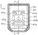
The differential signal D2N connected to TA19 (first differential signal contact) and the differential signal D2P connected to TA20 (second differential signal contact) are paired data communication signals for data communication, and are connected to the external connection terminal 209.
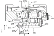
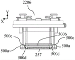
TA21 is connected to GND, and serves not only as a contact point for the reference potential but also as a terminal for controlling the wiring impedance of the differential signals D2N and D2P. TA21 corresponds to the fourth ground contact. The contacts TA01, TA04, TA06, TA18, and TA21 are connected to, for example, a GND part of the flexible substrate 259 shown in fig. 19A and 19B, which will be described later, and the GND part of the flexible substrate 259 is fixed to a metal member having a GND level of the accessory 200 with screws or the like, which are not shown. The metal member having the GND level includes, for example, the socket attachment leg 251 and a not-shown base plate inside the accessory 200.
Fig. 2A shows that an accessory connector 211 arranged on a socket provided on a lower portion of an accessory (strobe device) 200 is connected to a camera connector 141 arranged on an accessory socket provided on an upper portion of the camera 100. Fig. 2B shows a configuration example of 21 contacts TC01 to TC21 in the camera connector 141. TC01 is arranged at the right end as viewed from the object side, and 21 contacts up to TC21 are arranged in a row. The accessory shoe is attached by sliding it from the top side to the bottom side of fig. 2B relative to the accessory shoe with camera connector 141.
Fig. 2C shows a configuration example of 21 contacts TA01 to TA21 in the accessory connector 211. Similar to the camera connector 141, TA01 is arranged at the right end as viewed from the object side, and 21 contacts up to TA21 are arranged in a row. Generally, the contacts TA01 to TA21 and the corresponding contacts TC01 to TC21 are connected to each other. However, if excessive static pressure or impact is applied to the fitting 200, the contact may be disconnected (disconnect). In particular, when a force in the rotational direction acts in the direction of the arrangement of the contacts in the fitting 200, disconnection may occur at the end contacts.
Fig. 3A shows an enlarged appearance of excessive static pressure applied to the accessory 200 from the left side as viewed from the object side. At this time, a force acts on the contacts TC21 and TA21 and the adjacent contacts of the camera connector 141 and the accessory connector 211 in the opening direction, and a poor connection may occur. On the other hand, stronger force acts on the contacts TC01 and TA01 and the adjacent contacts in the connecting direction than in the normal state.
Fig. 3B shows an enlarged appearance of excessive static pressure applied to the fitting 200 from the right side viewed from the object side. At this time, a force acts on the contacts TC01 and TA01 and the adjacent contacts of the camera connector 141 and the accessory connector 211 in the opening direction, and a poor connection may occur. On the other hand, stronger force acts on the contacts TC21 and TA21 and the adjacent contacts in the connecting direction than in the normal state.
The present embodiment connects the contacts TC01 and TA01 and TC21 and TA21 at both ends of the camera connector 141 and the accessory connector 211 to GND. Therefore, even if poor connection temporarily occurs at the contact at one end due to excessive static pressure, GND connection can be ensured at the contact at the other end. Therefore, this structure can suppress the following: as a result of the reference potential of the accessory 200 becoming unstable due to the GND connection failure, each circuit and electric element are damaged.
In the case of the accessory 200 to which a part of the GND contact is missing due to a defect, a failure, or the like of the accessory connector 211, the camera control circuit 101 cannot detect the missing part of the GND contact. In this case, the operation current concentrates on the remaining GND contact, and the accessory 200 may malfunction in some cases.
Fig. 4A is a structural example for enabling the camera 100 to detect the connection state of the GND contact of the accessory 200, and shows a portion related to the ground contact extracted from the structure shown in fig. 1.
TC01, TC04, TC18, and TC21 are connected to input terminals P1, P2, P3, and P4 of the camera control circuit 101, respectively, and are pulled up to the camera microcomputer power supply VMCU _ C via resistors 1011rp _g1, 1021rp _g2, 1031rp _g3, and 1041rp _g4, respectively. The SW circuit 1, the SW circuit 2, the SW circuit 3, and the SW circuit 4 are connected to TC01, TC04, TC18, and TC21, respectively.
The SW circuit 1 is a switch circuit driven by a control signal of the camera control circuit 101, and when it is turned on by the control signal, TC01 is connected to GND. It is desirable, for example, for the SW circuit 1 to comprise a FET or for the SW circuit 1 to comprise a circuit with an impedance which is as small as possible when the operation is on and as large as possible when the operation is off. As shown in fig. 4A, the SW circuits 2, 3, and 4 each also have the same structure as that of the SW circuit 1.
Fig. 4B is a flowchart showing a sequence for determining the connection state of the ground terminal in the structure shown in fig. 4A. The camera control circuit 101 executes this processing and other processing described later according to a computer program. And S represents a step.
In S1001, the camera control circuit 101 monitors the signal level of the accessory attachment detection signal/ACC _ DET, and determines whether or not the accessory 200 is attached. If the signal level is Hi, the camera control circuit 101 returns to S1001 assuming that the accessory 200 is not attached and detection is performed again, and if the signal level is Lo, the camera control circuit 101 proceeds to S1002 assuming that the accessory 200 is attached.
In S1002, the camera control circuit 101 performs control such that the SW circuit 1 is turned on and the SW circuit 2, the SW circuit 3, and the SW circuit 4 are turned off, respectively.
In S1003, the camera control circuit 101 confirms the voltage level of the input terminal P1, and if the voltage level is the Lo level, it is determined that TC01 is connected to the ground contact, and if the voltage level is the Hi level, it is determined that TC01 is not connected to the ground contact.
Next, in S1004, the camera control circuit 101 performs control such that the SW circuit 2 is turned on and the SW circuit 1, the SW circuit 3, and the SW circuit 4 are turned off, respectively.
In S1005, the camera control circuit 101 confirms the voltage level of the input terminal P2, and if the voltage level is the Lo level, it is determined that TC04 is connected to the ground contact, and if the voltage level is the Hi level, it is determined that TC04 is not connected to the ground contact.
Next, in S1006, the camera control circuit 101 performs control such that the SW circuit 3 is turned on and the SW circuit 1, the SW circuit 2, and the SW circuit 4 are turned off, respectively.
In S1007, the camera control circuit 101 confirms the voltage level of the input terminal P3, and if the voltage level is the Lo level, it is determined that the TC18 is connected to the ground contact, and if the voltage level is the Hi level, it is determined that the TC18 is not connected to the ground contact.
Next, in S1008, the camera control circuit 101 performs control such that the SW circuit 4 is turned on and the SW circuit 1, the SW circuit 2, and the SW circuit 3 are turned off, respectively.
In S1009, the camera control circuit 101 confirms the voltage level of the input terminal P4, and if the voltage level is the Lo level, it is determined that the TC18 is connected to the ground contact, and if the voltage level is the Hi level, it is determined that the TC18 is not connected to the ground contact.
In S1010, the camera control circuit 101 performs control to turn on the SW circuit 1, the SW circuit 2, the SW circuit 3, and the SW circuit 4, respectively.
Such control enables the camera control circuit 101 to confirm the attachment state of the ground contact to the attached accessory 200, and determine whether or not to supply power to the accessory power supply circuit 202 and the like based on the ground connection state.
On the other hand, if the accessory 200 is tilted with respect to the camera 100 or the like when the accessory 200 is attached to the camera 100, only a part of the plurality of contacts TC01 to TC21 and TA01 to TA21 may be connected to each other. As shown in fig. 16A, 16B, and 16C, in the case where the Z direction is the attaching direction of the accessory 200 to the camera 100, the X direction is the direction in which the plurality of contacts TC01 to TC21 and TA01 to TA21 are aligned, and the Y direction is the direction perpendicular to the X direction and the Z direction, only a part of these contacts can be connected in the following case.
First, as shown in fig. 3A and 3B, in the case where the accessory 200 is tilted with respect to the camera 100 about an axis parallel to the Z direction, some of the plurality of contacts may be connected to each other on a side where the camera 100 and the accessory 200 are close to each other, but some of the plurality of contacts are disconnected from each other on another side where the camera 100 and the accessory 200 are separated from each other. Although not shown, in the case where the accessory 200 is tilted (twisted) with respect to the camera 100 about an axis parallel to the Y direction, some of the contacts on the side opposite to the side of the contacts connected to each other among the plurality of contacts are separated from each other.
As described later in detail with reference to fig. 5A and 5B, in the camera 100 and the accessory 200 according to the present embodiment, in a state where the accessory 200 is attached to the camera 100, an attachment detection process is performed before various communications. At this time, if the attachment detection contacts TC06 and TA06 are connected, the attachment detection process may be performed. After the attachment detection process via the contacts TC06 and TA06 is performed, a communication request signal/WAKE is output from the accessory 200 to the camera 100 via the contacts (hereinafter also referred to as communication request contacts) TC11 and TA11. By detecting the communication request signal/WAKE, the camera 100 performs various communications, and determines that the accessory 200 is in a communicable state. However, in a case where the camera 100 cannot detect the communication request signal/WAKE even if the attachment of the accessory 200 to the camera 100 is detected, the camera 100 determines that there is a communication error with the accessory 200. If the accessory 200 is tilted or twisted during the time the accessory 200 is being attached to the camera 100, only a part of the contacts are temporarily connected, it is determined that there is a communication error, and an error process such as an alarm or the like is performed, the user may misunderstand that the accessory 200 is malfunctioning.
Therefore, the present embodiment employs a contact configuration to reduce the occurrence of: even if attachment of the accessory 200 to the camera 100 is detected, the camera 100 cannot detect the communication request signal/WAKE.
As described above, in the case where the accessory 200 is tilted about the axis parallel to the Z direction with respect to the camera 100, as shown in fig. 3A, the contacts TC01 and TA01 and the adjacent contacts are connected and the contacts TC21 and TA21 and the adjacent contacts are disconnected, or as shown in fig. 3B, the contacts TC21 and TA21 and the adjacent contacts are connected and the contacts TC01 and TA01 and the adjacent contacts are disconnected.
The present embodiment uses the contacts TC06 and TA06 to detect attachment of the accessory 200 to the camera 100. As shown in fig. 3A, in the case where the contacts TC01 and TA01 are connected to each other, the adjacent contacts TC06 and TA06 are usually connected to each other. At this time, if the communication request contacts TC11 and TA11 are located near the contacts TC21 and TA21 at a distance, the camera 100 is less likely to detect the communication request signal/WAKE even if the attachment of the accessory 200 to the camera 100 is detected.
On the other hand, as shown in fig. 3B, in a state where the contacts TC21 and TA21 are connected to each other, the contacts TC06 and TA06 may be connected to each other. In this case, if the contacts TC11 and TA11 are arranged on the sides of the contacts TC01 and TA01 away from the contacts TC06 and TA06, the camera 100 is less likely to detect the communication request signal/WAKE even if attachment of the accessory 200 to the camera 100 is detected.
On the other hand, the present embodiment adopts the following contact arrangement. As shown in fig. 1, the attachment detection contacts TC06 and TA06 and the communication request contacts TC11 and TA11 are arranged between the contacts TC01 and TA01 closest to one end in the direction in which the plurality of contacts TC01 to TC21 and TA01 to TA21 are arranged (hereinafter referred to as the contact arrangement direction) and the contacts TC21 and TA21 closest to the other end in the direction. This configuration relationship will be referred to as a first configuration relationship. The attachment detection contacts TC06 and TA06 are arranged between the communication request contacts TC11 and TA11 and the contacts TC01 and TA 01. This configuration relationship will be referred to as a second configuration relationship. Then, in the contact arrangement direction, the distances between the attachment detecting contacts TC06 and TA06 and the communication requesting contacts TC11 and TA11 are made shorter than the distances between the communication requesting contacts TC11 and TA11 and the contacts TC21 and TA21. This configuration relationship will be referred to as a third configuration relationship. In the present embodiment, the contacts TC01 to TC21 and TA01 to TA21 are arranged at regular intervals, so that the distance between the contacts herein can be rephrased as the number of other contacts arranged between the contacts, and the short (or long) distance can be rephrased as the number of other contacts being small (or large).
In the present embodiment, the distance between the communication requesting contacts TC11 and TA11 and the contacts TC01 and TA01 is set to be equal to or smaller than the distance between the communication requesting contacts TC11 and TA11 and the contacts TC21 and TA21 in the contact arrangement direction. This configuration relationship will be referred to as a fourth configuration relationship. Specifically, the present embodiment arranges the communication request contacts TC11 and TA11 at the center between the contacts TC01 to TC21 and TA01 to TA21, and makes the distances between the communication request contacts TC11 and TA11 and the contacts TC01 and TA01 and the distances between the communication request contacts TC11 and TA11 and the contacts TC21 and TA21 equal to each other. The communication request contacts TC11 and TA11 are not necessarily arranged in the center between the contacts TC01 to TC21 and TA01 to TA21, but these two contacts are preferably arranged near the center.
The present embodiment makes the distance between the attachment detection contacts TC06 and TA06 and the contacts TC01 and TA01 in the contact arrangement direction equal to or larger than the distance between the attachment detection contacts TC06 and TA06 and the communication request contacts TC11 and TA11. This configuration relationship will be referred to as a fifth configuration relationship. In particular, the present embodiment arranges the attachment detection contacts TC06 and TA06 at the center between the communication request contacts TC11 and TA11 and the contacts TC01 and TA01, and makes the distances between the attachment detection contacts TC06 and TA06 and the contacts TC01 and TA01 and the distances between the attachment detection contacts TC06 and TA06 and the communication request contacts TC11 and TA11 equal to each other. The attachment detection contacts TC06 and TA06 are not necessarily arranged in the center between the communication request contacts TC11 and TA11 and the contacts TC01 and TA01, but it is preferable to arrange these two contacts in the vicinity of the center.
With the above-described contact configuration, in the inclined state shown in fig. 3A, if the attachment detection contacts TC06 and TA06 are connected to each other, the communication request contacts TC11 and TA11 are highly likely to be connected to each other, and in the inclined state shown in fig. 3B, the attachment detection contacts TC06 and TA06 are highly likely to be disconnected from each other even if the communication request contacts TC11 and TA11 are connected to each other. As a result, regardless of the state in which the accessory 200 is tilted, the occurrence of the following can be reduced: even if attachment of the accessory 200 to the camera 100 is detected, the camera 100 cannot detect the communication request signal/WAKE.
A comparative example of the case of exchanging the positions of the contacts TC06 and TA06 and the contacts TC11 and TA11 will now be described. That is, a case where the contacts TC11 and TA11 are used to detect attachment and the contacts TC06 and TA06 are used to detect the communication request signal/WAKE will be described. In this structure, in the case where the accessory 200 is tilted with respect to the camera 100 and the contacts TC01 and TA01 and the adjacent contacts are disconnected from each other, the contacts TC11 and TA11 for attachment detection may be connected to each other, but the contacts TC06 and TA06 for the communication request signal/WAKE may be disconnected from each other, which causes a communication error.
Therefore, in order to avoid a communication error, it is preferable to arrange the attachment detection contact instead of the contact for the communication request signal/WAKE on one end side in the contact arrangement direction as in the present embodiment.
As shown in fig. 20A to 20C and fig. 23A and 23B, which will be described later, in a structure in which the fitting 200 holds a plurality of contacts with a connection plug 256 that is a holding member made of a non-conductive material such as a resin material, the connection plug 256 may have a convex shape toward the lower side in the figure (the contact direction with the camera connector 141). In this case, among the plurality of contacts, the contact on one end side in the contact arrangement direction may be connected, but the contact on the other end side may be disconnected. However, the contact configuration shown in the present embodiment makes it possible to reduce the occurrence of communication errors even if a part of the contacts is opened when the accessory 200 is attached to the camera 100.
As described above, in the case where the accessory 200 is twisted with respect to the camera 100 about the axis parallel to the Y direction, some of the contacts on one end side in the contact arrangement direction among the plurality of contacts may be connected, but the other contacts on the other end side may be disconnected. In the case where such a state occurs in the process of attaching the accessory 200 to the camera 100, the connection timing is shifted between the plurality of contacts. If the connection timing is significantly shifted, the time lag from the attachment detection of the accessory 200 to the camera 100 until the detection of WAKE becomes long, and therefore it can be determined as a communication error. At this time, according to the twisting direction of the accessory 200, the connection of the contacts TC01 and TA01 or the contacts TC21 and TA21 is first started.
In the case where the contacts TC01 and TA01 side start to be connected, the closer the communication request contacts TC11 and TA11 are to the contacts TC21 and TA21, the longer the time lag from the attachment detection of the accessory 200 until the detection of the communication request signal/WAKE becomes. The longer the time lag, the easier it is to determine a communication error. On the other hand, in the case where the contacts TC21 and TA21 sides start to be connected and the communication request contacts TC11 and TA11 are arranged on the contacts TC01 and TA01 sides of the attachment detection contacts TC06 and TA06, a time lag occurs from the attachment detection of the accessory 200 until the detection of the communication request signal/WAKE.
On the other hand, the present embodiment adopts the above-described contact configuration, and shortens the time lag from the attachment detection of the accessory 200 until the detection of the communication request signal/WAKE regardless of which side of the contacts starts to be connected.
The present embodiment arranges contacts TC07, TA07 to TC10, and TA10 for SPI communication (communication using the second communication method) between the camera 100 and the accessory 200 at positions between the attachment detection contacts TC06 and TA06 and the communication request contacts TC11 and TA11. Contacts TC12, TA12, TC13, and TA13 for I2C communication (communication employing the first communication method) between the camera 100 and the accessory 200 are arranged on the opposite side of the attachment detection contacts TC06 and TA06 with respect to the communication requesting contacts TC11 and TA11 and at positions close to the communication requesting contacts TC11 and TA11.
After the camera 100 detects the communication request signal/WAKE, communication between the camera 100 and the accessory 200 is performed. Therefore, until communication between the camera 100 and the accessory 200 is performed, connection of the contact for communication cannot be confirmed. On the other hand, in the present embodiment, if the attachment detection contacts TC06 and TA06 and the communication request contacts TC11 and TA11 are connected to each other, the communication contacts TC07, TA07 to TC10, TA10, TC12, TA12, TC13, and TA13 arranged near and between these contacts, respectively, may be regarded as connected.
Since it can be considered that the positions between the attachment detection contacts TC06 and TA06 and the communication request contacts TC11 and TA11 are more reliably connected, the contacts for SPI communication performed after I2C communication are preferably arranged at the positions between the attachment detection contacts TC06 and TA06 and the communication request contacts TC11 and TA11.
As shown in fig. 4A, 4B, and fig. 12 and 20 to be described later, a structure in which the number of contacts is smaller than that of the camera 100 is conceivable as the structure of the accessory 200. Even in this structure, the attachment detection contact and the communication request contact are necessary contacts, and the attachment detection contact and the communication request contact may be configured under a similar concept to the structure in which the number of contacts is equal to the number of contacts of the camera 100. However, a part of the first to fifth configuration relationships described above may not be satisfied.
For example, assume a structure without the contact TA21 as shown in fig. 4A and 4B. In this configuration, the distance between the communication request contact TA11 and the contact TA01 is longer than the distance between the communication request contact TA11 and the contact TA20 in the contact arrangement direction. That is, the fourth configuration relationship is not satisfied. In addition, for example, a structure without the contacts TA01 to TA03 and TA19 to TA21 as shown in fig. 12 is assumed. In this structure, the distance between the attachment detection contact TA06 and the contact TA04 in the contact arrangement direction is shorter than the distance between the attachment detection contact TA06 and the communication request contact TA11. That is, the fifth configuration relationship is not satisfied.
As described above, in the structure in which the contact position at the end of the accessory 200 is different from the contact position at the end of the camera 100, a part of the first to fifth arrangement relationships may not be satisfied. In this case, it is assumed that the positions of the contacts at the end toward the camera 100 in the attached state are the positions of the contacts at the end of the accessory 200, and the attachment detection contacts and the communication request contacts may be configured to satisfy the first to fifth configuration relationships. Alternatively, as with the protrusion 256a shown in fig. 20A, 20B, and 20C, the attachment detection contact and the communication request contact may be configured to satisfy the first to fifth configuration relationships in consideration of the distance from the protrusion 256a rather than the distance from the contact at the end. The flowchart of fig. 5A shows processing executed by the camera control circuit 101 when the accessory 200 is attached to the camera 100.
In S401, the camera control circuit 101 as accessory detecting means monitors the signal level of the accessory attachment detection signal/ACC _ DET, and determines whether or not the accessory 200 is attached. If the signal level is Hi, the camera control circuit 101 returns to S401 and performs detection again assuming that the accessory 200 is not attached, and if the signal level is Lo, proceeds to S402 assuming that the accessory 200 is attached.
In S402, the camera control circuit 101 sets the power supply control signal CNT _ VACC1 to the Hi level to turn on the output of the accessory power supply circuit a131, and proceeds to S403. The accessory power supply circuit a131 outputs the accessory power supply VACC in response to the power supply control signal CNT _ VACC1 becoming Hi.
In S403, the camera control circuit 101 monitors the signal level of the overcurrent detection signal DET _ OVC, and determines whether an overcurrent is flowing. If the signal level is Lo, the camera control circuit 101 proceeds to S404 assuming that no overcurrent flows, and if the signal level is Hi, proceeds to S405 assuming that overcurrent flows, to perform error processing.
Fig. 6A schematically shows a change in signal in the case where the flow proceeds to S404 in the process of fig. 5A. IACC is the current of accessory power supply VACC. Since the accessory power supply VACC normally rises after the power control signal CNT _ VACC1 is set to Hi in S402, the overcurrent detection signal DET _ OVC remains at the Lo level.
Fig. 6B schematically shows a change of the above-described signal in the case where the flow proceeds to S405 in the process of fig. 5A. Since an overcurrent flows through the IACC after the power control signal CNT _ VACC1 is set to Hi in S402, the overcurrent detection signal DET _ OVC changes to the Hi level and notifies the camera control circuit 101. Upon receiving the notification of the overcurrent detection signal DET _ OVC, the camera control circuit 101 turns off the outputs of the accessory-use power supply circuits a131 and B132 as error processing to stop the power supply to the accessory 200. Therefore, even in the case where an overcurrent flows through the accessory power supply VACC, the camera control circuit 101 can detect the overcurrent and safely stop the system.
In general, in the case where an abnormal current flows through the accessory power supply VACC, it is assumed that the camera 100 and the accessory 200 are malfunctioning, but since the camera connector 141 and the accessory connector 211 are exposed to the outside, adjacent contacts may be short-circuited due to adhesion of foreign matter such as a metal piece or the like.
In the present embodiment, the accessory power supply VACC has a voltage of 3.3V, and the camera microcomputer power supply VMCU _ C and the accessory microcomputer power supply VMCU _ a have a voltage of 1.8V. Therefore, if a voltage of 3.3V is applied to the electric element operating at a voltage of 1.8V, the electric element may be damaged. Since the behavior after the short circuit depends on the characteristics of the electrical elements, the camera control circuit 101 may not always be able to detect the short circuit between the terminals. For example, since the I2C communication signal is at the Hi level in the communication standby state, even if a short circuit occurs at a voltage of 3.3V which is equal to or higher than 1.8V, an abnormality cannot be detected from the characteristics of the electrical element of the connection destination.
On the other hand, the present embodiment arranges the GND contacts TC04 and TA04 on one of both sides of the accessory power supply VACC contacts TC05 and TA05, and arranges the contacts TC06 and TA06 of the accessory attachment detection signal/ACC _ DET on the other side. As described above, the accessory attachment detection signal/ACC _ DET is connected to GND in the accessory 200. Therefore, even in the case where a short circuit occurs between the contacts, an overcurrent can be detected without applying 3.3V to the element operating at 1.8V and the system can be safely stopped.
As described above, if the accessory power supply VACC is supplied without connecting the GND contact, the reference potential of the accessory 200 becomes unstable, and thus each circuit and electric element may be damaged. When the device is operated, an external force may be applied to make the connection of the connector terminal unstable. On the other hand, by disposing the accessory power supply VACC contact and the GND contact adjacent to each other as in the present embodiment, it is possible to more effectively prevent connection of only the accessory power supply VACC contact, as compared with the case where the accessory power supply VACC contact and the GND contact are separate terminals.
The present embodiment connects the accessory attachment detection signal/ACC _ DET to GND in the accessory 200, but as in the accessory 200 shown in fig. 9, the accessory attachment detection signal/ACC _ DET may also be connected to GND via the resistor element Rd 231. The short circuit current can be reduced by connecting to GND via the resistor element Rd 231.
In this case, it is necessary to select the resistor element Rd231 having a resistance value as follows: a voltage of (Rd/(Rp + Rd)) × 1.8V obtained by dividing (divide) the voltage of 1.8V of the camera microcomputer power supply VMCU _ C by the resistor elements Rp134 and Rd231 satisfies the Lo level threshold (Vil) of the camera control circuit 101. For example, in the case where the low-level detection threshold (Vil) of the camera control circuit 101 is 0.33 times the power supply voltage, the resistance value of the resistor element Rd231 needs to be half or less of the resistor element Rp134 (10 k Ω). In the example of fig. 9, the resistance value of the resistor element Rd231 is set to 5k Ω.
Fig. 5B illustrates processing performed by the camera control circuit 101 when the accessory 200 having the structure illustrated in fig. 9 is attached to the camera 100. Since S411 to S413 are the same as S401 to S403 shown in fig. 5A, a description thereof will be omitted.
In S414 following S413, the camera control circuit 101 monitors the signal level of the accessory attachment detection signal/ACC _ DET, and determines whether the accessory attachment detection signal/ACC _ DET contacts TC06 and TA06 are short-circuited with the accessory power sources VACC contacts TC05 and TA05. If the signal level is Lo, the camera control circuit 101 proceeds to S415 assuming that no short circuit has occurred, and if the signal level is Hi, proceeds to S416 assuming that a short circuit has occurred to perform error processing.
Fig. 6C schematically shows the state of the above signals in the case where the accessory power supply VACC and the accessory attachment detection signal/ACC _ DET are short-circuited in the accessory 200 having the configuration of fig. 9 to which the resistor element Rd231 (5 k Ω) is added. After the power supply control signal CNT _ VACC1 is set to Hi in S402, since the current is limited by the resistor element Rd231, no overcurrent flows in the IACC.
On the other hand, the voltage of the accessory power supply VACC is applied to the accessory attachment detection signal/ACC _ DET. Once the signal level of the accessory attachment detection signal/ACC _ DET becomes Hi due to the interrupt processing or the like, the camera control circuit 101 sets the power supply control signal CNT _ VACC1 to Lo in error processing, and stops outputting the accessory power supply VACC (supplying power to the accessory 200). Therefore, the system can be safely stopped without continuously applying 3.3V to the terminals of the element operating at 1.8V.
As shown in fig. 10, the accessory 200 can be controlled such that the accessory attachment detection signal/ACC _ DET becomes Lo level (GND potential) by the accessory control circuit 201 via the NPN transistor 212 as a switching section. The camera control circuit 101 can always detect the accessory 200 if the accessory 200 is attached to the camera 100 in the configuration shown in fig. 1, but the accessory control circuit 201 can notify the attachment of the accessory 200 to the camera 100 at an arbitrary timing in the configuration shown in fig. 10.
As shown in fig. 11, accessory 200 can be configured to connect resistor element Rd231 in series with NPN transistor 212. In this case, as with the structure of fig. 1, the resistance value needs to be half or less of the resistor element Rp134 (10 k Ω).
As described above, the present embodiment can maintain the safety of the system including the camera 100 and the accessory 200 and prevent both from being damaged even if the power supply contact and the adjacent contact are short-circuited.
Fig. 7 shows an example of functions of the FNC1 signal to the FNC4 signal as the function signals connected to the contacts TC14 to TC17 and the contacts TA14 to TA17 for each type of the accessory 200 (here, the microphone device and the strobe device).
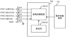
In the microphone device, the FNC2 signal to FNC4 signal are used as a digital audio (I2S: inter-IC sound standard) data bus to transmit audio data. Fig. 8A shows a structural example of the functional circuit 206 in the case where the accessory 200 is a microphone device.
The audio processing circuit 206A1 in the function circuit 206 is a codec circuit for converting an audio signal input from the microphone 206A2 into a digital audio (I2S) data format, and is controlled by the accessory control circuit 201. The accessory control circuit 201 can set the sampling frequency and resolution by controlling the audio processing circuit 206 A1. In this embodiment, the sampling frequency is 48kHz and the resolution is 32 bits. The microphone 206A2 is, for example, a MEMS-IC microphone or an electret condenser microphone.
TA14 is the FNC1 signal which is not used as the I2S data bus and is connected to GND. In the present embodiment, an unused function signal is connected to GND, but the present invention is not limited to the present embodiment, and connection to a reference potential which is a stable potential other than the GND potential (0V), such as a power supply potential and an L level (low potential) or an H level (high potential) of a signal, may be made.
The FNC2 signal connected to TA15 (DATA contact) is an audio DATA signal (DATA), which is a signal output from the accessory 200 to the camera 100.
The FNC3 signal connected to TA16 (LRCLK contact) is an audio channel clock signal (LRCLK), which is a signal output from the accessory 200 to the camera 100.
The FNC4 signal connected to TA17 (BCLK contact) is an audio bit clock signal (BCLK), which is a signal output from the camera 100 to the accessory 200.
In the present embodiment, since the sampling frequency is 48kHz and the resolution is 32 bits as described above, the LRCLK frequency is 48kHz and the BCLK frequency is 3.072MHz. The maximum frequency of DATA is 1.536MHz, which is half the period of CLK.
In the contact configuration according to the present embodiment, the reference potential contacts TA18 and TC18 connected to the GND potential as the reference potential are arranged next to the contacts TA17 and TC17 to which the FNC4 signal (BCLK) having the highest frequency among the function signal contacts to which the function signal is connected. A flexible substrate is generally disposed for signal wiring to the accessory shoe interface. To reduce product cost, the flexible substrate may have a single-sided specification, and the substrate wiring is made in the same configuration as the contact configuration. The present embodiment arranges the GND contact as the reference potential contact next to the functional signal contact connected to the signal having the highest frequency among the functional signals. This structure can suppress radiation noise (EMI) from the functional signal contact, interference with signals connected to other contacts, and crosstalk with signals other than the I2S data bus.
The present embodiment connects the contacts TA18 and TC18 next to the contacts TA17 and TC17 connected to the FNC4 signal (BCLK) having the highest frequency to the GND potential as the reference potential, but the present invention is not limited to this example, and the same effect can be obtained even if connected to a stable reference potential other than the GND potential.
Fig. 8B is an example showing a structure in which audio data is added with respect to fig. 8A. The purpose of adding audio data is to increase the number of channels and resolution.
The FNC4 signal connected to TA17 is an audio bit clock signal (BCLK) which is the same as that shown in FIG. 8A.
On the other hand, the FNC1 signal connected to the TA14 is an audio channel clock signal (LRCLK), which is a signal output from the accessory 200 to the camera 100.
The FNC2 signal connected to TA15 is an audio DATA signal (DATA 2), which is a signal output from the accessory 200 to the camera 100.
The FNC3 signal connected to TA16 operates as an audio DATA signal (DATA 1), which is a signal output from the accessory 200 to the camera 100.
In this way, in the case where the audio data signal is added to increase the amount of audio data and two signals are used, configuring the signals in the order of higher frequencies arranged closer to the GND terminal can provide a structure that is relatively efficient in preventing crosstalk.
Fig. 8C shows a structural example of the functional circuit 206 in the case where the accessory 200 is a strobe device. The light-emitting circuit 206B1 in the functional circuit 206 is a strobe light-emitting circuit including an IGBT, a trigger coil, and the like, and controls light emission of the light emitter 206B 2. The light emitter 206B2 includes a xenon tube or the like, and emits illumination light to illuminate the object. The charging circuit 206B3 includes a transformer, a switching FET, a capacitor, and the like, and accumulates charges for causing the light emitter 206B2 to emit light.
The FNC1 signal connected to TA14 is a light emission synchronization Signal (STARTX) for controlling the light emission timing of the light emitter 206B2, and is a signal output from the camera 100 to the accessory 200. The FNC2 to FNC4 signal is not used in the strobe device and no signal is connected to these contacts.
The present embodiment OPENs (OPEN) the unused function signal contact, but the present invention is not limited to the present embodiment, and may be connected to a stable reference potential such as a power supply potential and an L or H level of a signal or the like in accordance with the contacts TC15 to TC17 as connection destinations of the contacts TA15 to TA 17.
In the strobe device, only the FNC1 signal is used in the function signal. Although the light emission synchronization Signal (STARTX) is not a periodically generated signal, the camera 100 assigns GND to the FNC1 signal when the microphone device is connected, to prevent the structure of the camera control circuit 101 from becoming complicated.
Further features of the contact arrangement according to the present embodiment will now be described. Both SDA (first signal) connected to the contacts TC12 and TA12 as the first signal contacts and SCL (second signal) connected to the contacts TC13 and TA13 as the second signal contacts are signals for I2C communication. These signals are transmitted through open-drain communication. Since both the SDA and the SCL are pulled up to the camera microcomputer power supply VMCU _ C, both are signals having relatively high impedance during the communication standby, and are susceptible to crosstalk.
Therefore, the present embodiment assigns the communication request signal (fourth signal)/WAKE to the contacts TC11 and TA11 as the fourth signal contacts next to the SDA contacts TC12 and TA 12. As described above, the communication request signal/WAKE is a signal for making a communication request from the accessory 200 to the camera 100.
Fig. 15A shows the timing at which the accessory 200 makes a communication request to the camera 100 and performs I2C communication. As shown in fig. 15A, the signal level of the communication request signal/WAKE is changed from the Hi level to the Lo level before the I2C communication through the SCL and the SDA. This is because I2C communication is performed in response to the change. Thus, placing the contacts TC11 and TA11 of the communication request signal/WAKE at and near the SDA contacts for I2C communication may keep the SDA of the communication request signal/WAKE free from crosstalk.
As shown in fig. 15A, the control to change the signal level of the communication request signal/WAKE from the Lo level to the Hi level after the I2C communication can keep the SDA of the communication request signal/WAKE free from crosstalk.
The FNC1 signal is assigned to contacts TC14 and TA14 as the third signal contacts next to SCL contacts TC13 and TA 13. As described above, since GND is assigned to the FNC1 signal in the microphone device, SCL can be kept free from crosstalk.
In the strobe device, a light-emission synchronization signal (STARTX: third signal) as the FNC1 signal is assigned to the contacts TC14 and TA14 next to the SCL contacts TC13 and TA 13. Fig. 15B shows the timing at which the accessory 200 makes a communication request to the camera 100 and performs I2C communication and stroboscopic light emission. As shown in fig. 15B, at the timing (time period) when the light emission synchronization signal is output, I2C communication is not performed between the camera 100 and the accessory 200 to handle control of strobe light emission at the highest priority. In other words, the light emission synchronization signal is a signal whose signal level changes before (or after) the I2C communication but does not change during the I2C communication. This structure can keep the SCL of the light emission synchronization signal from crosstalk.
Therefore, the present embodiment arranges the STARTX contact on one of both sides of the SDA contact and the SCL contact, and arranges the/WAKE contact on the other side, thereby achieving good I2C communication.
Similar to the SDA, the present embodiment sets the communication request signal/WAKE connected to the contacts TC11 and TA11 next to the SDA contacts TC12 and TA12 as an open-drain signal. In comparison with the push-pull type communication request signal/WAKE being a push-pull system, crosstalk to the SDA can be suppressed when the signal level of the communication request signal/WAKE changes.
SCLK connected to SCLK contacts TC07 and TA07 is a clock signal for SPI communication, and operates at a driving frequency of 1MHz in the present embodiment. In the present embodiment, the attachment detection contacts TC06 and TA06 next to the SCLK contacts TC07 and TA07 are used to transmit the accessory attachment detection signal/ACC _ DET. As described above, the accessory attachment detection signal/ACC _ DET is a signal having a potential equivalent to GND when the accessory 200 is attached to the camera 100. Thus, the contact configuration may prevent cross talk between SCLK and signals other than the SPI bus.
MOSI connected to the other contacts TC08 and TA08 next to SCLK contacts TC07 and TA07 is a data signal transmitted from the camera control circuit 101 to the accessory control circuit 201 through SPI communication. In general, the timing of MOSI output level changes in SPI communication is synchronized with the timing of SCLK output level changes. Therefore, by placing MOSI contacts TC08 and TA08 next to SCLK contacts TC07 and TA07, crosstalk between SCLK and MOSI may be suppressed.
The MISO connected to the other contacts TC09 and TA09 next to the MOSI contacts TC08 and TA08 is a data signal transmitted from the accessory control circuit 201 to the camera control circuit 101 in the SPI communication. In general, similarly to MOSI, the timing of MISO output level change is synchronized with the timing of SCLK output level change in SPI communication. Therefore, by placing the MISO contacts TC09 and TA09 next to the MOSI contacts TC08 and TA08, crosstalk between MOSI and MISO can be suppressed.
The CS connected to the other contacts TC10 and TA10 next to the MISO contacts TC09 and TA09 is a communication request signal transmitted from the camera control circuit 101 to the accessory control circuit 201 in SPI communication. In general, the CS in SPI communication maintains a constant output level from the communication request until the communication is completed. Therefore, by arranging the CS contacts TC10 and TA10 next to the MISO contacts TC09 and TA09, crosstalk to MISOs can be suppressed.
The communication request signal/WAKE connected to the contacts TC11 and TA11 adjacent to the CS contacts TC10 and TA10 is a signal for making a communication request from the accessory control circuit 201 to the camera control circuit 101. As described above, the communication request signal/WAKE is an open-drain signal and thus is relatively susceptible to crosstalk. Therefore, the present embodiment arranges the contacts TC10 and TA10 of the CS, the signal level of which changes relatively infrequently, next to the contacts TC11 and TA11 for the communication request signal/WAKE, and can suppress crosstalk to the communication request signal/WAKE.
The differential signals requiring impedance control are connected to contacts TC01 to TC03 and TA01 to TA03 and contacts TC19 to TC21 and TA19 to TA21 located at and near both ends of the camera connector 141 and the accessory connector 211 (these will be hereinafter collectively referred to as both end sides). A flexible substrate is generally disposed for signal wiring to the accessory shoe interface. In order to achieve a desired wiring impedance on the flexible board, it is necessary to maintain a distance between the lines of the differential signals and GND to be wired in parallel. In the case of using the two-sided board, a mesh-shaped GND wiring is generally formed on the back side of the differential signal. Therefore, signal wiring requiring impedance control has relatively large restrictions on wiring design compared to general single-ended signals.
On the other hand, the present embodiment connects the differential signal requiring impedance control to the contacts at both ends of the camera connector 141 and the accessory connector 211, thereby relatively reducing the relationship with other signals and improving the degree of freedom in wiring design.
The differential signal can be transmitted at a high speed of about several hundreds of Mbps to several Gbps (such as USB and PCIe), and is suitable for transmitting a large amount of data between devices. On the other hand, differential signaling may not be used, depending on the type of accessory 200. An accessory that does not use differential signals does not need contacts assigned to differential signals, and therefore, accessory cost can be reduced by deleting contacts.
Fig. 12 shows a structural variation of the fitting 200 shown in fig. 1. More specifically, the accessory 200 has a structure in which the contacts TA01 to TA03 and TA19 to TA21, and signals and circuits connected to these contacts are omitted. That is, the fitting 200 in fig. 12 has 15 contacts. In the configuration of fig. 12, differential signals are assigned to the contacts TC01 to TC03 and TC19 to TC21 located at both ends of the camera connector 141. On the other hand, the accessory 200 that does not require differential signaling adopts a contact configuration in which the contacts for differential signaling are eliminated from the accessory connector 211, and includes only the contacts required by the accessory 200.
The accessory 200 in fig. 12 sets contacts TC04 and TA04 and contacts TC18 and TA18 near both ends of the camera connector 141 and the accessory connector 211 as GND contacts. With such a contact configuration, even in the accessory 200 connected to a part of the contacts of the camera connector 141, the contacts at both ends of the accessory connector 211 can be set as GND contacts. This structure can prevent the GND contact from being opened even in the case where excessive static pressure or impact is applied to the accessory 200.
The direct attachment of accessory 200 to camera 100 has been described. Referring now to fig. 13, an intermediate fitting 300 attached between the camera 100 and the fitting 200 will be explained. The camera 100 and the accessory 200 have the above-described structure. The intermediate accessory 300 includes an extension cable for extending the distance between the camera 100 and the accessory 200, and an adaptor for simultaneously attaching a plurality of accessories to the camera 100, and the like. The present embodiment will be described with the intermediate fitting 300 as an extension cable. In the structure in fig. 13, the intermediate fitting 300 corresponds to a fitting, and the fitting 200 corresponds to other fittings.
The intermediate accessory 300 has a camera socket and an accessory socket that are attachable to the camera 100 and the accessory 200, respectively, and are each provided with a camera-side intermediate connector 311 and an accessory-side intermediate connector 312. The camera side intermediate connector 311 has 21 contacts TM01 to TM21 arranged in a row, and is a connector for making electrical connection with the camera 100. The contacts TM01 to TM21 are each in one-to-one contact with the contacts TC01 to TC21 in the camera connector 141.
On the other hand, the accessory side intermediate connector 312 has 21 contacts TN01 to TN21 arranged in a row, and is a connector for making electrical connection with the accessory 200. The contacts TN01 to TN21 are each in one-to-one contact with the contacts TA01 to TA21 in the accessory connector 211.
An intermediate accessory 300 having such a contact configuration can provide power and communication in the same manner as if the accessory 200 were directly attached to the camera 100. At this time, the intermediate accessory 300 may receive power from the camera 100, or power from the camera 100 may be directly transmitted to the accessory 200. The power supply in the present embodiment includes a case where the power supply from the camera 100 is transmitted to the accessory 200 as it is and the power is not supplied to the accessory 300.
In fig. 13, the number of contacts of the camera-side intermediate connector 311 is the same as that of the camera connector 141, and the number of contacts of the accessory-side intermediate connector 312 is the same as that of the accessory connector 211, but these numbers may not necessarily be equal to each other.
Fig. 14 shows a modification of the structure of fig. 13 relating to the fitting 200 and the intermediate fitting 300. Although differential signals are connected to the contacts TC01 to TC03 and TC19 to TC21 on both ends of the camera connector 141, the differential signals may not be required depending on the function of the accessory 200. The structure of fig. 14 eliminates the contacts to which the differential signals are connected from the camera side intermediate connector 311 and the accessory side intermediate connector 312 and the accessory connector 211. That is, the intermediate fitting 300 and the fitting 200 in fig. 14 each have 15 contacts. Thus, a contact configuration including only the contacts required for the intermediate fitting 300 and the fitting 200 is adopted.
A connection structure between the camera 100 and the external strobe unit 120 as an example of the accessory 200 will now be described in detail.
Fig. 16A shows the camera 100 viewed from the oblique back surface side. Fig. 16B shows how the external flash unit 120 is attached to the accessory shoe 1123 of the camera 100. Fig. 16C illustrates that the external strobe unit 120 is attached to the camera 100 as viewed from the oblique back surface side.
The image pickup optical system is disposed on the front side (field side) of the camera 100, and the image display unit 107 is disposed on the back side of the camera 100. A top cover 150 as an exterior member is provided on the top surface of the camera 100, and a accessory shoe 1123 is provided to the top cover 150. On the other hand, in the external flash unit 120, a camera connector 1206 is provided at the bottom of the external flash unit 120.
As shown in fig. 16B, the external strobe unit 120 is slid in a direction parallel to the front side in the Z direction (attachment side in the first direction) with respect to the camera 100 to engage the camera connector 1206 and the accessory shoe 1123 with each other. Thereby, the external flash unit 120 can be attached to the camera 100. The front side in the Z direction is a direction from the back side to the front side of the camera 100, i.e., a direction from the image display unit 107 side toward the imaging optical system side. The X direction (second direction), the Y direction (third direction), and the Z direction (front-rear direction) shown in fig. 16A, 16B, and 16C and subsequent figures are generally used. The X direction is a direction perpendicular to the Z direction in a horizontal plane when the Z direction is parallel to the horizontal direction, and is a width direction of the camera 100. The Y direction is a direction perpendicular to the Z direction and the X direction, and is a height direction of the camera 100.
The accessory shoe 1123 of the camera 100 will now be described in detail. Fig. 17A shows the top cover 150 and the exploded accessory shoe 1123. Fig. 17B shows the assembled accessory shoe 1123. The assembly direction of the accessory shoe 1123 on the top cover 150 is the Y direction.
The accessory shoe 1123 includes an engagement member 151, a connection terminal connector 152, a shoe table 153, and an accessory shoe spring 154. The engaging member 151 is a member for holding the external flash unit 120 by engagement with the external flash unit 120. The connection terminal connector 152 includes a plurality of connection terminals 152a, which are arranged at regular intervals in the X direction on a connector base member 152e as a holding member made of a resin material or the like, and held by the connector base member 152 e. The connection terminals 152a correspond to the contacts TC01 to TC21 in the camera connector 141 shown in fig. 1.
In the connection terminal connector 152, as shown in fig. 17B, a connection terminal 152a is arranged on the front side in the Z direction (front side of the camera 100) as the attaching direction of the external strobe unit 120. An engagement hole portion 156 to be engaged with a lock pin 252 of the external strobe unit 120 shown in fig. 19A is provided behind the connection terminal connector 152 in the Z direction (on the back side of the digital camera 100).
In a state where the external flash unit 120 is attached to the accessory shoe 1123, the connection terminal 152a is electrically connected to the external flash unit 120. Each of the plurality of connection terminals 152a is electrically connected to a flexible substrate 158 disposed on the lower side of the top cover 150 in the Y direction. The flexible substrate 158 is connected to a main substrate, not shown, of the camera 100. Thus, communication is available between the external flash unit 120 and the camera 100 when the external flash unit 120 is attached to the accessory shoe 1123.
The socket base 153 is a housing member surrounding the joint member 151 and the connection terminal connector 152. The accessory shoe retaining member 155 is a structural skeleton that retains the engagement member 151. As shown in fig. 17A, the accessory shoe holding member 155, the flexible substrate 158, the top cover 150, the shoe table 153, and the connection terminal connector 152 are fastened to the engagement member 151 by four screws 157 inserted therein. Thereby, these members are positioned and fixed to each other. By disposing four screws 157 one by one in four regions equally divided in the X direction and the Z direction, the above components can be connected in a well-balanced manner.
Fig. 18A shows the configuration of the top surface side of the joining member 151, and fig. 18B shows the configuration of the bottom surface side of the joining member 151. Fig. 18C shows the structure of the connection terminal connector 152 on the top surface side. Fig. 24 shows an accessory shoe 1123 viewed from the insertion direction (attachment direction) of the external strobe unit 120.
The joining member 151 is formed by bending a metal plate into a ring shape such that end faces of the bent ends face each other and contact at a seam 151 a. The engaging member 151 has a pair of engaging portions 151b and a coupler 151c that couples the pair of engaging portions 151b together. The engagement member 151 has a pair of first screw hole portions 151d for fastening the screw 157, and a pair of second screw hole portions 151e. The engaging member 151 has an engaging hole portion 156 to be engaged with a locking pin 252 of the external strobe unit 120.
As shown in fig. 18A and 12, the pair of engaging portions 151b are separated by a first width (hereinafter, engaging portion interval) 151aa in the X direction. A holding member 254 of an external strobe unit 120 shown in fig. 19B, which will be described later, is inserted into the engaging part interval 151aa. The pair of first screw hole portions 151d are provided at a predetermined interval in the X direction, and serve as a pair of first fastening hole portions provided apart from each other in the X direction at the rear (back side) in the Z direction. The pair of second screw hole portions 151e are provided at a predetermined interval in the X direction, and serve as a pair of second fastening hole portions provided apart from each other in the X direction in front of the Z direction. The engaging hole portion 156 is formed at a position engageable with the locking pin 252 of the external strobe unit 120 in a region sandwiched between the pair of first screw hole portions 151 d.
In the connection terminal connector 152, as shown in fig. 17B and 18C, a plurality of connection terminals 152a are exposed. In the pitch direction (X direction) in which the plurality of connection terminals 152a are aligned, the position of the camera connector 1206 is determined by the engagement portion interval 151aa of the engagement member 151. Thus, the holding member 254 of the external strobe unit 120 is positioned with respect to the connection terminal connector 152 by the engaging member 151.
On both sides of a connection terminal connector 152 (connector base member 152 e) as one example of the camera connector 141 shown in fig. 1, which sandwich a plurality of connection terminals 152a in the X direction on the front side in the Z direction, contact surfaces and groove portions shown in fig. 24 are formed. That is, there are formed a contact face 152b that contacts and positions accessory shoe 1123 in the Z direction when external flash unit 120 is attached, and a groove portion 152c into which accessory shoe 1123 is inserted. Each groove portion 152c is formed to extend from the contact surface 152b to the front side (attachment side) in the Z direction, and has a slope portion 152d facing the inside and obliquely upper side (so as to have an inclination with respect to the X direction). The portion of the groove portion 152c above the inclined surface portion 152d extends outward in the X direction from the tip end position of the inclined surface portion 152d. This is to prevent a dent (sink) from being generated in the slope portion 152d during resin molding in the case where the slope portion 152d is formed up to the tip of the groove portion 152c.
As shown in fig. 24, in the X direction, outermost inner faces 152ccc of groove portions 152c in connector base member 152e of accessory shoe 1123 are located outside the inner end faces (engaging portion intervals 151 aa) of the pair of engaging portions 151b of engaging member 151, and inside outermost inner faces 151bb of engaging member 151.
A slope start position 152cc, which is an end (lower end) of the slope portion 152d on the bottom surface side of the groove portion 152c, is provided inside the joint portion interval 151aa. Thereby, a region for providing a contact surface 152b that contacts a later-described contact portion 251b of the camera connector 1206 and positions the contact portion 251b in the Z direction can be secured. Providing the shape of the slope starting from the slope starting position 152cc can expand the space into which the outlet device (camera connector 1206 described later) of the external strobe unit 120 is inserted, and can secure the degree of freedom of the shape of the outlet device. As a result, the socket device of the external strobe unit 120 can be sufficiently formed in a shape that protects the connection terminals.
The external strobe unit 120 will now be explained. Fig. 19A shows the external strobe unit 120 viewed from the camera connector 1206 side (bottom side in the Y direction). Fig. 19B isbase:Sub>A cross section taken along the linebase:Sub>A-base:Sub>A in fig. 19A, and shows the internal configuration of the camera connector 1206. Fig. 20A shows a camera connector 1206. However, the base portion 250 and the locking lever 253, which will be described later, are omitted. Fig. 20B shows the camera connector 1206 viewed from the front in the Z direction.
The camera connector 1206 is disposed on the bottom side (the top side of fig. 19A) in the Y direction of the base part 250 of the external strobe unit 120 as shown in fig. 19B when it is attached to the accessory shoe 1123 of the camera 100. The camera connector 1206 includes a socket attachment leg (engaging member, socket board) 251, a lock pin 252, a lock lever 253, a holding member 254, a connection plug 256, and a Y-direction holding member 258.
The socket attachment leg 251 as the socket engagement member is an engagement member that engages with and is held by the accessory socket 1123 of the camera 100. That is, the socket attachment leg 251 is an engagement member attachable to the engagement member 151 of the accessory socket 1123 and detachable from the engagement member 151 of the accessory socket 1123 on the external flash unit 120 side.
Large stress is applied to the accessory shoe 1123 and the camera connector 1206 due to pressure for maintaining the attached state and external force (impact or the like) acting on the external flash unit 120. The socket attachment leg 251 is manufactured by machining a metal plate (sheet metal) to ensure high mechanical strength against such large stress.
The lock pin 252 is a member for preventing the external flash unit 120 from falling off in a state where the camera connector 1206 (socket attachment leg 251) is attached to the accessory socket 1123, and is held on the socket attachment leg 251 movable in the Y direction. More specifically, the locking pin 252 is slidably held in the Y direction by the Y-direction holding member 258. The locking lever 253 and the Y-direction holding member 258 are held by the holding member 254.
With the external strobe unit 120 attached to the accessory shoe 1123 and the lock lever 253 rotated, the Y-direction holding member 258 is moved downward in the Y-direction in fig. 19B by a cam portion, not shown. At this time, the locking pin 252 also moves downward in the Y direction in fig. 19B together with the Y-direction holding member 258. Thereby, the locking pins 252 protrude from the socket attachment legs 251 and engage with the engagement hole portions 156 provided in the engagement members 151 of the accessory socket 1123. The locking pin 252 and the engagement hole portion 156 function as a positioning member in the Z direction for ensuring electrical connection between the external flash unit 120 and the camera 100.
A connection plug 256, which is one example of the accessory connector 211 shown in fig. 1, is provided on the front side in the Z direction of the camera connector 1206, is made of a non-conductive material (dielectric material) such as a resin material or the like, and is integrated with the holding member 254. The outermost width T in the X direction of the connection plug 256 is narrower than the width W in the X direction of the socket attachment leg 251. Thereby, a region for providing the contact portions 251b on the socket attachment legs 251 is secured. The connection plug 256 has a plurality of connection terminals 257 for contacting and communicating with the plurality of connection terminals 152a of the accessory shoe 1123 shown in fig. 18C. The connection terminal 257 corresponds to the contacts TA01 to TA21 of the accessory connector 211 shown in fig. 1.
The plurality of connection terminals 257 are provided in one-to-one correspondence with the plurality of connection terminals 152a, and are held by the holding member 254 to extend in the Z direction and be aligned in the X direction. Each connection terminal 257 has a front end portion 257a that contacts the corresponding connection terminal 152a. The front end portion 257a is exposed to the lower side in the Y direction (-Y direction) and the front end side in the Z direction (+ Z direction) with respect to the connection plug 256. Each of the connection terminals 257 has a shape extending rearward in the Z direction from the front end portion 257a, and has an extended portion 257B which displaces the front end portion 257a upward in the Y direction in fig. 19B by elastic deformation when the front end portion 257a comes into contact with the connection terminal 152a. A vertical extension portion 257c extending upward in the Y direction is formed at a rear end of the extension portion 257b in the Z direction. At the upper end of the vertical extending portion 257c, a flexible substrate connector 257d is provided, which flexible substrate connector 257d is connected to a not-shown main substrate of the external strobe unit 120 and to a flexible substrate 259 inserted into the holding member 254 from the top side in the Y direction.
The extending portion 257b has a stepped portion 257e having a step in the Y direction at the center in the Z direction. As described above, the extending portion 257b may be elastically deformed in the Y direction. However, in the case where the distance L in the Z direction of the extended portion 257b is short, a sufficient amount of deformation cannot be obtained, and the durability is reduced. As a result, the connection terminal 152a and the front end portion 257a are repeatedly attached and detached, and the extension portion 257b may be easily damaged. Therefore, providing the step portion 257e to the extended portion 257b can ensure a sufficient distance L without causing the extended portion 257b to interfere with the socket attachment leg 251.
As shown in fig. 20A and 20B, at both ends of the connection plug 256 in the X direction, there are a pair of protrusion portions 256a that protrude downward in the Y direction (third direction) to sandwich the plurality of connection terminals 257. That is, a pair of protruding portions 256a is provided on both outer sides of the plurality of connection terminals 257. As shown in fig. 20B, the lower front end portion 256d of each protruding portion 256a protrudes below a line obtained by connecting the lower ends of the front end portions 257a of the connection terminals 257 to protect the connection terminals 257 from external forces such as pressure and impact. That is, the front end portion 257a of the connection terminal 257 is disposed above (inside) a line obtained by connecting the lower front end portions 256d of the pair of protruding portions 256a.
On the outer side (outer face) in the X direction of each protrusion 256a, there is a slope portion 256b serving as an outer face extending obliquely upward from the lower leading end portion 256d and facing obliquely downward, i.e., having an inclination with respect to the X direction. In other words, each of the projecting portions 256a is provided with a slope portion 256b on a side not facing the plurality of connection terminals 257 such that the width of each projecting portion 256a in the X direction at a position close to the front end in the Y direction is smaller than the width in the X direction at a position away from the front end. Since each of the protruding portions 256a has such a shape, the connection plug 256 can be inserted into the groove portion 152c having the inclined surface portion 152d in the connection terminal connector 152.
The slope 256b has a function of releasing external force such as pressure and impact from the connection plug 256 to prevent the connection plug from being damaged. For example, fig. 20C shows a case where an external force is applied to the connection plug 256 from the X direction. Fig. 20C shows the connection plug 256 viewed from the front in the Z direction.
The external force from the X direction is defined as F as a vector 1 . External force F acting on the inclined surface 256b 1 Is decomposed into the component force F in the direction along the inclined surface portion 256b in the vector space according to the addition theorem 2 And a component force F in a direction perpendicular to the inclined surface portion 256b 3 . At theta by an external force F 1 In the case of the angle formed with the inclined surface portion 256b, the component force can be calculated by the following equation (1)F 2 And component force F 3 。
F 2 =F 1 cosθ
F 3 =F 1 sinθ (1)
In the case where the inclined surface portion 256b is provided, θ is 0 ° < θ <90 °. In this range, the following holds.
F 2 <F 1
F 3 <F 1 (2)
Due to component force F 2 Escape in the direction along the inclined surface portion 256b, and thus the component force F 3 Is the only force that affects the connector plug 256. As described above, due to the component force F 3 Less than component force F 1 Therefore, even if an external force of a certain degree is applied, the connection plug 256 can be prevented from being damaged.
By forming the slope portions 256b on both sides in the X direction such that the width thereof in the X direction is narrowed toward the lower side in the Y direction, not only the external force from the X direction but also the external force from the bottom side in the Y direction can be partially released.
Fig. 25 shows a partially enlarged connection plug 256 as viewed from the Z direction. In the Y direction, it is assumed that B is the height from the lower front end 256d of the protrusion 256a to the top surface of the connection plug 256 (the height of the connection plug including the protrusion), and a is the height from the lower front end 256d (slope start position 256 c) to the slope 256B of the upper end of the slope 256B. At this time, a is preferably one fifth or more, more preferably one quarter or more, one third or more, or half or more as shown in fig. 13, of B. That is, the slope portion 256b is formed to have a significant size having a function for releasing the external force from the X direction, and is different from the chamfered shape generally provided at the corner of the protrusion portion. For the above-described function of releasing the external force, the inclination angle θ of the slope portion 256b with respect to the X direction is preferably set in the range of 45 ° ± 20 °.
In order to ensure that the contact portions 251b on the socket attachment legs 251 have a sufficient area with respect to the contact face 152b of the accessory socket 1123 as the positioning portion in the Z direction, the width in the X direction between the slope start positions 256c at the lower front end portions 256d of the slope portions 256b on both sides may be set as short as possible. The present embodiment sets the width in the X direction between the slope starting positions 256c inside the width V in the X direction of the holding member 254. In other words, in the present embodiment, the width in the X direction of the contact portion, which is the contact surface 152b of the contact fitting socket 1123 and is provided between the socket engagement portion 251a and the protrusion portion 256a in the X direction, in the region in contact with the contact surface 152b is variable according to the position in the Y direction. In the present embodiment, as the position is closer to the front end of the protrusion 256a in the Y direction, the width of the region in contact with the contact surface 152b becomes wider in the X direction. In addition, in other words, in the present embodiment, the lower front end portion 256d, which is the lower end in the Y direction of the front end portion in the Z direction, is not located below the plurality of connection terminals 257 in the Y direction and is not located outside the end of the socket engaging portion 251a on the side of the plurality of connection terminals 257 in the X direction. In the present embodiment, the lower front end portion 256d is located below the plurality of connection terminals 257 in the Y direction. In the present embodiment, the lower front end portion 256d is disposed at a position inside the end of the socket engagement portion 251a on the side of the plurality of connection terminals 257 in the X direction. This configuration ensures a sufficient area for the contact portion 251 b.
The camera connector 1206 has a configuration of fastening the socket attachment leg 251 and the holding member 254. Details of the fastening structure will be described later.
The holding member 254 can be inserted into the engaging portion space 151aa of the engaging member 151 of the accessory shoe 1123 shown in fig. 18A, and has a coupler 254a having a width V in the X direction shorter than the width W of the shoe attachment leg 251. The widths W and V are defined by Japanese Industrial Standard (JIS) B7101-1975 "camera accessory attaching seat and attaching foot". When the coupler 254a is engaged with the engagement member 151, the position of the external flash unit 120 with respect to the camera 100 is determined in the X direction. The socket attachment leg 251 is urged toward the upper side in the Y direction when it comes into contact with the elastically deformable portion 154a of the accessory socket spring 154 as the urging member shown in fig. 17A and 17B. Thereby, the top surface of the socket engagement portion 251a is brought into contact (press-contact) with the bottom surface of the engagement member 151, and the position of the external strobe unit 120 with respect to the camera 100 is determined in the Y direction.
When the contact portion 251b of the socket attachment leg 251 is in contact with the contact face 152b of the front side in the Z direction of the connection terminal connector 152, the position of the external flash unit 120 with respect to the camera 100 is determined in the Z direction.
The holding member 254 is also a configuration for coupling the socket attachment leg 251 and the base portion 250, and the locking pin 252 and the connection terminal 257 are arranged inside the coupler 254 a.
Next, a fastening structure between the holding member 254 and the socket attachment leg 251 is explained below. Fig. 21A shows the camera connector 1206 viewed from the upper side in the Y direction, and fig. 21B shows a cross section taken along line B-B of fig. 21A.
A pair of first screws 260a and a pair of second screws 260b as fastening members for fastening the socket attachment leg 251 to the holding member 254 penetrate the holding member 254 and are fastened to the socket attachment leg 251. At this time, the socket attachment leg 251 is stably held by the holding member 254 by arranging one screw in each of four regions approximately equally divided in the X direction and the Z direction in a well-balanced manner. As described above, the socket attachment leg 251 is a component to which large stress is applicable. Therefore, by fastening the metal socket attachment leg 251 to the holding member 254 with the pair of first screws 260a and the pair of second screws 260b configured in a well-balanced manner, it is possible to ensure a required mechanical strength.
As shown in fig. 21B, a plurality of connection terminals 257 are arranged in an area S sandwiched by a pair of first screws 260a and a pair of second screws 260B. The width between the pair of first screws 260a and the width between the pair of second screws 260b are narrower than the width between the lower front end portions 256d of the projecting portions 256a of the connection plug 256, the width V of the holding member 254, the outermost side width T of the connection plug 256, and the width W of the socket attachment leg 251.
Fig. 26 shows a cross section of the accessory shoe 1123 viewed from the Z direction in a state where the camera connector 1206 is attached to the accessory shoe 1123. The figure shows the sizes T and V of the camera connector 1206 and the positional relationship between the respective components of the camera connector 1206 and the respective components of the accessory shoe 1123.
In fig. 26, as described above, the top surface of the socket engagement portion 251a of the camera connector 1206 contacts the bottom surface (ceiling surface) of the engagement member 151 of the accessory socket 1123 for positioning in the Y direction.
On the other hand, lower tip portion 256d and inclined surface portion 256b of protrusion 256a of connection plug 256 in camera connector 1206 do not each contact the bottom surface of groove portion 152c of accessory shoe 1123 and inclined surface portion 152d. The gap between lower tip portion 256d of protrusion 256a and the bottom surface of groove portion 152c of accessory shoe 1123 is set as small as possible. Thereby, when an external force in the X direction is applied to external flash unit 120, lower tip portion 256d of protrusion portion 256a can come into contact with the bottom surface of groove portion 152c of accessory shoe 1123, and the floating amount (inclination with respect to accessory shoe 1123) of connection plug 256 can be reduced.
The gap between the inclined surface portions 256b and 152d and the gap between the inner end surface 152ccc of the groove portion 152c and the outer end surface of the connection plug 256 are each set large to some extent. Thereby, when an external force in the X direction is applied to the external strobe unit 120, it is possible to prevent a load from being applied to the connection terminals 257 and 152a.
In groove portion 152c of accessory shoe 1123, the relationship between the height of groove portion 152c in the Y direction (the height from the bottom surface of groove portion 152c to the ceiling surface of engagement member 151) and the height of inclined surface portion 152d in the Y direction is the same as the relationship between height B of connection plug 1256 in camera connector 1206 and height a of inclined surface portion 256B. It is also preferable that the inclination angle of the slope portion 256b with respect to the X direction is also set within a range of 45 ° ± 20 °, as is the inclination angle θ of the slope portion 256b in the camera connector 206.
The above embodiments describe that the surface shape of the inclined surface portion 256b provided on the protruding portion 256a is flat, but the inclined surface portion 256b may be a curved surface having a curvature. That is, the inclined surface portion 256b may have a surface inclined with respect to the X direction.
This embodiment can secure an area for providing a larger number of connection terminals than ever and an area for protecting the shapes of these connection terminals and for positioning between components in the compact camera connector 1206 and the accessory shoe 1123.
A description will now be given of a modification of the external strobe unit 120. Fig. 22A shows the external strobe unit 120 as viewed from the camera connector 1206 side (lower side in the Y direction). Fig. 22B showsbase:Sub>A cross section taken along linebase:Sub>A-base:Sub>A of fig. 22A, and shows the internal configuration of the camera connector 1206. Fig. 23A shows a camera connector 1206. However, the base portion 250 and the locking lever 253 are omitted. Fig. 23B shows the camera connector 1206 viewed from the front in the Z direction.
The camera connector 1206 is provided on the lower side in the Y direction (upper side in fig. 22A) of the base part 250 of the external strobe unit 120 as shown in fig. 22B in a state where it is attached to the accessory shoe 1123 of the camera 100. The camera connector 1206 has a socket attachment leg 300a, a locking pin 252, a locking lever 253, a holding member 254, a connection plug 300b, a Y-direction holding member 258, and a socket cover 301.
The socket attachment leg 300a is an engagement member for engaging the external flash unit 120 with the accessory socket 1123 of the camera 100, as with the socket attachment leg 251 in the above-described embodiment. That is, the shoe attachment leg 300a is an engagement member attachable to the engagement member 151 of the accessory shoe 1123 and detachable from the engagement member 151 of the accessory shoe 1123 on the external flash unit 120 side.
In the above-described embodiment, the socket attachment leg 251 and the resin holding member 254, which are metal socket boards, are formed as separate members so as to give priority to mechanical strength. On the other hand, in this modification, the socket attachment leg 300a and the holding member 254 are formed as an integral member from a resin material (non-conductive material). Therefore, the pair of first screws 260a and the pair of second screws 260b described in the foregoing embodiments are not required, and the space for disposing the connection terminals 257 becomes wide, and thus a larger number of connection terminals 257 can be disposed. As a result, the external strobe unit 120 can communicate more information with the camera 100 via the camera connector 1206 and the accessory shoe 1123.
The connection plug 300b is provided on the front side in the Z direction of the camera connector 1206, and is formed as an integral member with the holding member 254 made of a non-conductive resin material in the present embodiment. As in the above-described embodiment, the outermost width T of the connection plug 300b in the X direction is made narrower than the width W of the socket attachment leg 300a in the X direction, so that an area for providing the contact portion 300e is secured in the socket attachment leg 300 a. The connection plug 300b has a plurality of connection terminals 257 for contacting and communicating with the plurality of connection terminals 152a of the accessory shoe 1123 shown in fig. 18C.
The socket cover 301 is a housing attached to the holding member 254, and is a member for protecting the plurality of connection terminals 257. The shape of the connection terminal 257 is the same as that of the above-described embodiment, and a stepped portion 257e is provided to ensure a sufficient distance L in the Z direction of the extension portion 257b without interfering with the socket cover 301.
The shape of the connection plug 300b is also the same as that of the connection plug 256 of the foregoing embodiment, and a pair of protrusions 300c protruding downward in the Y direction are provided at both ends of the connection plug 300b in the X direction to sandwich the plurality of connection terminals 257. As shown in fig. 23B, the lower front end portion 300k of each protruding portion 300c protrudes below a line obtained by connecting the lower ends of the front end portions 257a of the connection terminals 257 to protect the connection terminals 257 from external forces such as pressure and impact. That is, the front end portion 257a of the connection terminal 257 is disposed above (inside) a line obtained by connecting the lower front end portions 300k of the pair of projecting portions 300 c.
Even in the present embodiment, a slope portion 300f extending obliquely upward from the lower front end portion 300k and facing obliquely downward is provided on the outer side in the X direction of each protrusion portion 300 c. Each of the protrusions 300c having such a shape enables insertion of the connection plug 300b into the groove portion 152c having the inclined surface portion 152d in the connection terminal connector 152 described in the foregoing embodiment. As described in the foregoing embodiment, the slope portion 300f has a function of releasing external force such as pressure and impact to the connection plug 300b to prevent the connection plug from being damaged.
As in the previous embodiment, it is desirable to make the distance in the X direction between the slope start positions 300g at the lower leading end portions 300k of the slope portions 300f on both sides as short as possible. Therefore, the slope start positions 300g on both sides are set within the width V in the X direction of the holding member 254 to sufficiently secure the area of the contact portion 300e of the receptacle attachment leg 300 a.
The holding member 254 is formed to be insertable into and engaged with the engaging part interval 151aa of the engaging member 151 shown in fig. 18A, and has a coupler 300h having a width V in the X direction shorter than the width W of the receptacle attachment leg 300 a. As with the previous embodiments, the width W and the width V are defined by JIS B7101-1975 "Camera accessory attachment base and attachment foot". When the coupler 300h is engaged with the engagement member 151, the position of the external flash unit 120 with respect to the camera 100 is determined in the X direction. The socket attachment leg 300a is urged toward the upper side in the Y direction when it comes into contact with the elastically deformable portion 154a of the accessory socket spring 154 shown in fig. 17A and 17B, whereby the top face of the socket engagement portion 300d comes into contact with the bottom face (ceiling face) of the engagement member 151. Thereby, the position of the external strobe unit 120 with respect to the camera 100 is determined in the Y direction.
When the contact portion 300e of the receptacle attachment leg 300a comes into contact with the contact face 152b on the front side in the Z direction of the connection terminal connector 152, the position of the external strobe unit 120 relative to the camera 100 is determined in the Z direction. The holding member 254 is also a configuration for coupling the socket attachment leg 300a and the base portion 250, and the locking pin 252 and the connection terminal 257 are arranged inside the coupler 300 h.
In the present embodiment, the case where the camera 100, the accessory 200, and the intermediate accessory 300 have 21 or 15 contacts is described, but the number of contacts may be other numbers.
In the present embodiment, the microphone device and the strobe device have been described as the accessory 200, but the accessory according to the present invention includes various devices such as an electronic viewfinder unit and the like in addition to the microphone device and the strobe device. The present embodiment describes a camera as an electronic apparatus, but the electronic apparatus according to the present invention also includes various electronic apparatuses other than cameras.
Next follows another embodiment of external flash unit 120.
Fig. 27A shows the external strobe unit 120 as viewed from the camera connector 1206 side (lower side in the Y direction). Fig. 27B illustratesbase:Sub>A cross section taken along linebase:Sub>A-base:Sub>A of fig. 27A, which shows the internal configuration of the camera connector 1206. Fig. 28A shows the camera connector 1206, but the base portion 250 and the lock lever 253 are omitted. Fig. 28B shows the camera connector 1206 viewed from the front in the Z direction.
Fig. 29A illustrates that the external strobe unit 120 is attached to the camera 100 when the camera 100 is viewed from the oblique back side. Fig. 29B shows a section taken along line B-B of fig. 29A in which the camera connector 1206 (socket attachment leg 400 a) of the external strobe unit 120 is being inserted into the accessory socket 1123 (engaging member 151) of the camera 100. Fig. 29C shows the same cross section as that of fig. 29B, and shows the socket attachment leg 400a held by the accessory shoe 1123 after the insertion of the socket attachment leg 400a into the accessory shoe 1123 is completed.
The socket attachment leg 400a is an engagement member for engaging the external flash unit 120 with the accessory socket 1123 of the camera 100. That is, the shoe attachment leg 400a is an engagement member for the external strobe unit 120 that is attachable to and detachable from the engagement member 151 of the accessory shoe 1123.
The socket attachment leg 400a and the holding member 400 are formed as an integral member from a resin material (non-conductive material). This structure eliminates the need for the pair of first screws 260a and the pair of second screws 260b, and increases the space for disposing the connection terminals 257, so that a large number of connection terminals 257 can be disposed. As a result, the external strobe unit 120 can communicate more information with the camera 100 via the camera connector 1206 and the accessory shoe 1123.
The connection plug 400b is provided on the front side in the Z direction of the camera connector 1206, and is formed as a member integral with the holding member 400 made of a non-conductive resin material. Making the outermost width T in the X direction of the connection plug 400b narrower than the width W in the X direction of the socket attachment leg 400a can secure an area for providing the contact portion 400e in the socket attachment leg 400a. The connection plug 400B has a plurality of connection terminals 257 for contacting and communicating with the plurality of connection terminals 152a of the accessory shoe 1123 shown in fig. 17A and 17B. The socket cover 301 is a housing attached to the holding member 400, and serves as a member that protects the plurality of connection terminals 257. Each of the connection terminals 257 has the same shape as that of the other embodiments, and a stepped portion 257e is provided to ensure a sufficient distance L in the Z direction of the extension portion 257b without interfering with the socket cover 301.
The connection plug 400b also has the same shape as that of the connection plug 256 of the other embodiments, and a pair of protrusion portions 400c protruding downward in the Y direction are provided at both ends of the connection plug 400b in the X direction to sandwich the plurality of connection terminals 257. As shown in fig. 28B, the lower front end portion 400k of each protruding portion 400c protrudes to a position below a line connecting the lower ends of the front end portions 257a of the connection terminals 257 to protect the connection terminals 257 from external forces such as pressure and impact. That is, the front end portion 257a of the connection terminal 257 is disposed above (inside) a line connecting the lower front end portions 400k of the pair of protrusion portions 400 c.
Even in the present embodiment, a slope portion 400f extending obliquely upward from the lower tip portion 400k and facing an obliquely lower side is provided on the outer side in the X direction of each protrusion portion 400 c. Since each of the protrusions 400c has such a shape, the connection plug 400b can be inserted into the groove portion 152c having the inclined surface portion 152d in the connection terminal connector 152 described in the first embodiment. As described in other embodiments, the slope portion 400f has a function of releasing external force such as pressure and impact to the connection plug 400b and preventing the connection plug 400b from being damaged.
The distance in the X direction between the slope start positions 400g at the lower front end portions 400k of the slope portions 400f on both sides may be set as short as possible. Therefore, the slope start positions 400g on both sides are set within the width V in the X direction of the holding member 254 to sufficiently secure the area of the contact portion 400e of the receptacle attachment leg 400a.
The holding member 400 has a connector 400h, which connector 400h is insertable into the engaging portion space 151aa of the engaging member 151 shown in fig. 18A, is engageable with the engaging member 151, and has a width V shorter than the width W in the X direction of the socket attachment leg 400a. The dimensions of the width W and the width V are defined in JIS B7101-1975 "Camera Accessory Mount and mounting foot". When the connector 400h is engaged with the engagement member 151, the position of the external strobe unit 120 with respect to the camera 100 is determined in the X direction.
The holding member 400 also has a configuration for connecting the socket attachment leg 400a and the base portion 250 to each other, and the locking pin 252 and the connection terminal 257 are arranged within the connector 400 h.
As shown in fig. 29A to 29C, the socket attachment leg 400A has a contact range (first range) 400j that contacts the elastically deformable portion 154a of the accessory socket spring 154 shown in fig. 17A and 17B. When the contact range 400j contacts the elastically deformable portion 154a of the accessory shoe spring 154, the shoe attachment leg 400a is biased toward the upper side in the Y direction, and the top surface of the shoe engagement portion 400d contacts the bottom surface of the engagement member 151. Arrow F in fig. 29B and 29C represents the biasing force with the accessory shoe spring 154. Thereby, the position of the external strobe unit 120 in the Y direction with respect to the camera 100 is determined. The contact range 400j corresponds to a bias range biased by the elastically deformable portion 154a of the accessory shoe spring 154 in a state where the external flash unit 120 is being attached to the accessory shoe 1123 and when the attachment of the external flash unit 120 to the accessory shoe 1123 is completed. The contact range 400j is arranged on both sides of the plurality of connection terminals 152a on the front side (front surface side of the camera 100) in the Z direction as the attaching direction.
The socket attachment leg 400a has a non-contact range (second range) 400i that does not contact the elastically deformable portion 154a of the accessory socket spring 154. This non-contact range 400i corresponds to a non-biased range that is not biased by the elastically deformable portion 154a of the accessory shoe spring 154 in a state where the external flash unit 120 is being attached to the accessory shoe 1123 and when the attachment of the external flash unit 120 to the accessory shoe 1123 is completed. In fig. 16C, since there is a gap between accessory shoe spring 154 and non-contact range 400i, the biasing force of accessory shoe spring 154 against non-contact range 400i is 0.
In the present embodiment, the thickness in the Y direction of the non-contact range 400i is set to be larger than the thickness in the same direction of the contact range 400j. The thickness of the contact range 400j is set to be the same as those of the first and second embodiments. The thickness in the Y direction of the non-contact range 400i is set to be larger than that of the contact range 400j for the following reason.
The resin socket according to the present embodiment is inferior in strength to the metal socket in the case where both have the same shape. Therefore, the strength can be ensured by increasing the thickness of the socket attachment leg 400a in the Y direction in the non-contact range 400i. Since the strength calculated by the area moment of inertia increases in proportion to the square of the thickness, the strength can be efficiently increased by increasing the thickness in the Y direction. By making the length in the Z direction of the non-contact range 400i longer than the length in the Z direction of the contact range 400j, greater strength can be ensured.
By making the thickness of the contact range 400j equal to that of the other embodiments, the socket attachment leg 400a can become common according to JIS, and the elastically deformable portion 154a of the accessory socket spring 154 can be prevented from being plastically deformed beyond the yield point. When the external flash unit 120 is attached to the accessory shoe 1123, the thickness in the Y direction of the contact range 400j is made equal to that of the other embodiments, so that the attachment load is equal to that of the other embodiments.
Since the non-contact range 400i is provided on the attachment side in the Z direction of the contact range 400j, even in a state where the external flash unit 120 is being attached to the accessory shoe 1123, the elastically deformable portion 154a can be prevented from being plastically deformed beyond the yield point.
In the present embodiment, non-contact range 400i is a non-biased range that is not biased by elastically deformable portion 154a of accessory shoe spring 154 in a state where external flash unit 120 is being attached to accessory shoe 1123 and when attachment of external flash unit 120 is completed. Alternatively, the non-contact range 400i may be biased by the accessory shoe spring 154 in a state where the external flash unit 120 is being attached to the accessory shoe 1123 and when the attachment of the external flash unit 120 is completed. In this case, in a state where the external flash unit 120 is held by the accessory shoe 1123, a range in which the biasing force of the accessory shoe spring 154 is smaller than that of the contact range 400j can be set to a range corresponding to the non-contact range 400i. That is, the second range of the socket attachment leg 400a may be thicker than the first range and may have a biasing force (including 0) exerted by the accessory socket spring 154 that is less than the first range of biasing forces.
When the contact portion 400e of the receptacle attachment leg 400a contacts the contact face 152b on the front side in the Z direction of the connection terminal connector 152, the position in the Z direction of the external flash unit 120 with respect to the camera 100 is determined.
Next follows another embodiment of accessory shoe 423. Fig. 30 shows the top cover 450 and the detached accessory shoe 423 separated from the camera 100.
The accessory shoe 423 includes an engaging member 451, a connection terminal connector 452, a shoe table 453, and an accessory shoe spring 154. The engaging member 451 is a member to be engaged with the external flash unit 120 and thereby hold the external flash unit 120. The connection terminal connector 452 includes a plurality of connection terminals 452a. The socket base 453 is a case member surrounding the joining member 451 and the connection terminal connector 452. The accessory shoe retaining member 155 is a structural skeleton that retains the engagement member 451.
The accessory shoe holding member 155, the flexible printed circuit (FPC, flexible substrate) 458, the top cover 450, the shoe table 453, and the connection terminal connector 452 are fastened to the engagement member 451 by four screws 157 inserted into holes formed therein. Thereby, these members are positioned and fixed to each other.
When external flash unit 120 is attached to accessory shoe 423, connection terminal 452a is electrically connected to external flash unit 120. The plurality of connection terminals 452a are each electrically connected to an FPC 458 disposed on the Y-direction lower side of the top cover 450.
The FPC 458 is connected to a main substrate of the camera 100, not shown. Therefore, when the external flash unit 120 is attached to the accessory shoe 423, communication between the external flash unit 120 and the camera 100 becomes available. To connect the FPC 458 to the internal electronics of the camera 100, the socket stand 453 has an opening 453a and the top cover 450 has an opening 450a.
Referring now to fig. 31A to 31C, the drip-proof configuration will be explained. Fig. 31A shows the accessory shoe 423 incorporated in the shoe 453 as viewed from below (Y direction). Fig. 31B shows only the socket stand 453 viewed from the-Y direction. Fig. 31C showsbase:Sub>A cross section taken along linebase:Sub>A-base:Sub>A of fig. 31A.
An engagement hole portion 452b engageable with the lock pin 252 of the external strobe unit 120 shown in fig. 19A is provided at the rear of the connection terminal connector 452 in the Z direction (on the back side of the camera 100). The engaging member 451 has a screw hole portion 451a to which the screw 157 is fastened. The socket base 453 is provided with a through hole 453c through which the screw 157 penetrates.
A rectangular frame-shaped drip-proof member 453b is provided around the opening 453a provided in the socket base 453. The drip-proof member 453b is an elastic member such as an elastic body, and is integrated with the socket base 453. In the present embodiment, the drip-proof member 453b is integrated with the socket base 453 by two-shot molding.
As shown in fig. 31C, the drip-proof member 453b interferes with (contacts) the connection terminal connector 452, and is compressed to prevent water from entering the camera 100 through the opening 453a in the receptacle stage 453 and the opening 450a in the top cover 450. The drip-proof member 453b may be made of an elastic member such as sponge or silicon as a member separated from the socket stand 453.
The drip-proof member 453b is arranged in a projection plane of the + Y direction from the connection terminal connector 452 (in an XZ projection plane). The screw hole 451a and the through hole 453c are disposed inside the drip-proof member 453b. This configuration can also prevent water from entering through the screw hole portion 451a and the through hole portion 453c.
Therefore, the drip-proof member 453b disposed around the opening 453a of the socket stand 453 and the connection terminal connector 452 interfere with each other to prevent water from entering the inside of the camera 100.
The present embodiment can secure an area for a larger number of connection terminals than ever and a shape for protecting the connection terminals and a positioning area between components in the small outlet device and the accessory outlet device.
Second embodiment
The accessory shoe of the camera 100 and the shoe device of the external flash unit 120 according to the second embodiment of the present invention are explained next. In the case where the camera connector 1206 shown in fig. 20A to 20C is attached to the accessory shoe 1123 shown in fig. 17A and 17B, the following problem may occur.
Fig. 32 shows camera connector 1206 biased in the X direction as viewed from the + Y direction about to be attached to accessory shoe 1123. In this state, the contact portions 251b of the socket attachment legs 251 of the camera connector 1206 contact the front ends of the accessory sockets 1123, and the camera connector 1206 cannot be further inserted into the accessory sockets 1123 in the Z direction. In addition, the socket attachment leg 251 is not engaged with the engagement member 151, but a portion of the connection plug 256 is engaged with the engagement member 151. In this state, when an external force is applied to the camera connector 1206 in a tilting direction (the + Y direction corresponding to the counterclockwise direction about the X axis), a load tends to concentrate on a part of the connection plug 256. Therefore, if an external force in an oblique direction is applied to the camera connector 1206 in this state, the connection plug 256 partially engaged with the engagement member 151 may be damaged. Therefore, the present embodiment uses the following shape to alleviate the above problem.
Fig. 33 shows the accessory shoe 523 of the camera 100 according to the present embodiment. The accessory shoe 523 includes an engagement member 551, the connection terminal connector 152, the shoe table 153, and the accessory shoe spring 154. The engaging member 551 is a member engageable with the external flash unit 120 and configured to hold the external flash unit 120, and has inclined (oblique) portions (second inclined portions) 551a on both sides thereof in the X direction. Each inclined portion 551a is a portion inclined outward in the X direction toward the-Z direction tip.
The connection terminal connector 152 includes a plurality of connection terminals 152a. The socket base 153 is a housing member that surrounds the engaging member 551 and the connection terminal connector 152.
Fig. 34A shows a camera connector 2206 provided to the external flash unit 120 according to the present embodiment, but the base portion 250 and the lock lever 253 are omitted. Fig. 34B shows the camera connector 2206 viewed from the front side in the Z direction.
The holding member 500 of the camera connector 2206 includes a socket attachment leg 500a as an engaging member (socket engaging portion) engageable with the engaging member 551 of the accessory socket 523, and a connection plug 500b protruding on the front end side in the Z direction of the socket attachment leg 500 a. The connection plug 500b corresponds to a terminal protection unit that protects the plurality of connection terminals 257. When the top surface of the receptacle attachment leg 500a engaged with the engaging member 551 contacts the ceiling surface of the engaging member 551 in the + Y direction (third direction), the position in the Y direction of the receptacle attachment leg 500a is determined.
Side (chamfered) inclined surfaces 500c are provided on both sides in the X direction on the top surface on the root side of the connection plug 500b, and a front end inclined (chamfered) portion 500d as a first inclined portion is provided on both sides in the X direction on the front end side of the connection plug 500b. In the present embodiment, each of the receptacle attachment leg 500a and the connection plug 500b is made of a non-conductive resin material and is formed as one component. Alternatively, only the socket attachment leg 500a may be made of a metal material.
Fig. 35 shows that a camera connector 2206 biased to one side of the X direction (-X direction) when viewed from the + Y direction is about to be attached to the accessory shoe 523 in the present embodiment. In this state, the socket attachment leg 500a of the camera connector 2206 contacts the engagement member 551 of the accessory socket 523, and the camera connector 2206 cannot be further inserted into the accessory socket 523 in the Z direction. In addition, the receptacle attachment leg 500a is not engaged with the engagement member 551, but a part of the connection plug 500b is engaged with the engagement member 551.
At this time, a side slope 500c is provided at a portion of the connection plug 500b engaged with the engagement member 551. Each side inclined surface 500c is an inclined surface inclined such that the connection plug 500b descends in the-Y direction (a direction opposite to the third direction) in a region from the inside to the outside in the X direction. Therefore, when an external force is applied to the camera connector 2206 in the oblique direction, the side inclined surface 500c contacts the engagement member 551 and slides, thereby guiding the connection plug 500b to move to the other side (+ X direction) in the X direction. This configuration can prevent the connection plug 500b from being damaged. The side slope 500c may be a flat slope having a flat surface or a curved slope having a curved surface. In the present embodiment, the slope connected to the side slope 500c is also formed at the front end slope 500d and the outermost front end portion of the connection plug 500b.
That is, the connection plug 500b has a slope continuously inclined (skewed) from the front end in the X direction to the front end in the Z direction. The term "continuously inclined" herein means that the inclined portions are connected and includes inclined surfaces having different inclination angles between the inclined surface facing the X direction and the inclined surface facing the Z direction, and inclined surfaces curved between the inclined surface facing the X direction and the inclined surface facing the Z direction.
Fig. 36A, 36B, and 37 show the front end inclined portion 500d of the connection plug 500B and the inclined portion 551a of the engaging member 551 when viewed from the + Y direction. As shown in fig. 36A, the front end inclined portion 500d is inclined inward in the X direction by a first angle θ 1 toward the front end in the + Z direction as the insertion direction (attachment direction) of the camera connector 2206 into the accessory shoe 523. On the other hand, as shown in fig. 36B, the inclined portion 551a has a shape in which the tip in the-Z direction is inclined outward in the X direction by a second angle θ 2.
The present embodiment sets the first angle θ 1 to the second angle θ 2 or more (θ 1 ≧ θ 2). The first angle θ 1 may be set to be greater than the second angle θ 2 (θ 1> θ 2).
Fig. 37 shows the camera connector 2206, tilted by an angle θ about the Y-axis with respect to the Z-direction, about to be inserted into the accessory shoe 523.θ is an angle of θ 2 or greater.
Due to the above-described relationship between θ 1 and θ 2, in this state, the connection plug 500b does not contact the engagement member 551 alone in the + Y direction before the receptacle attachment leg 500a engages with the engagement member 551 of the accessory receptacle 523. Thereby, even if an external force is applied to the camera connector 2206 in an oblique direction in this state, the connection plug 500b can be prevented from being damaged.
Thereafter, when the connection plug 500b and the receptacle attachment leg 500a advance toward the engagement member 551 in the + Z direction while reducing the inclination angle θ with respect to the Z direction, the receptacle attachment leg 500a alone or the receptacle attachment leg 500a and the connection plug 500b may contact the engagement member 551 in the + Y direction at the same time.
Fig. 38A and 38B show a positional relationship between a position (inclination starting position) as a starting point of an inclined surface provided at the front end of the connection plug 500B and the plurality of connection terminals 257. Fig. 38A shows the camera connector 2206 viewed from the + Y direction to visualize the positions of the plurality of connection terminals 257 which overlap with the connection plug 500b and cannot be seen. Fig. 38B showsbase:Sub>A cross section taken along linebase:Sub>A-base:Sub>A of fig. 38A. The plurality of connection terminals 257 are each partially exposed with respect to the connection plug 256 on the lower side in the Y direction (-Y direction) and the front end side in the Z direction (+ Z direction).
As shown in fig. 38A, the width of the side slope 500c in the X direction is wider than the width between adjacent connection terminals in the plurality of connection terminals 257. In the case where L is the width in the X direction of the side slope 500c and L is the width between adjacent connection terminals included in the plurality of connection terminals 257, for example, a relationship of L >3L is established. As shown in fig. 38A, in the X direction, the position of the start point of the side slope 500c (inclination start position) is farther from the center of the holding member 500 than the connection terminals located at both ends of the plurality of connection terminals 257. This configuration can form the side slope 500c while maintaining the strength of the connection plug 500b so that the connection plug 500b is prevented from being damaged even if an external force in the X direction is applied to the connection plug 500b.
As shown in fig. 38B, the front ends of the plurality of connection terminals 257 are located on the + Z direction side of the position (slope start position) as the start point of the slope at the front end of the connection plug 500B. In the case where the slope widens in the + Z direction, the connection plug 500b more easily moves when an external force is applied to the camera connector 2206 in the slope direction, so that the connection plug 500b can be easily prevented from being damaged. On the other hand, when attempting to widen the slope in the + Z direction, the connection plug 500b may become large in the Z direction. Therefore, with the above-described structure, it is possible to form the slope having a predetermined width or more at the outermost front end portion while suppressing the size of the connection plug 500b in the Z direction.
Therefore, in the above configuration, the front end of the connection plug 500b is inclined, so that the connection plug 500b is not easily damaged when an external force is applied to the camera connector 2206 in an inclined direction. Even in the case where the socket attachment legs 500a provided on both sides of the connection plug 500b are engaged with the engagement members 551, the socket attachment legs 500a may be damaged when a strong external force is applied to the camera connector 2206 in an oblique direction. Therefore, the front end of each socket attachment leg 500a may be inclined. If the front ends of the socket attachment legs 500a are inclined, the socket attachment legs 500a become less likely to be damaged, and the respective inclined portions serve as guides for inserting and ejecting the camera connector 2206 with respect to the accessory socket 523 and facilitate the insertion and ejection.
On the other hand, when the top surface of the receptacle attachment leg 500a engaged with the engaging member 551 contacts the ceiling surface of the engaging member 551 in the + Y direction, the position of the receptacle attachment leg 500a is determined in the Y direction, so that the front end of the receptacle attachment leg 500a may not be inclined based on the positioning accuracy in the Y direction. While the inclined configuration is adopted, the area of the inclined portion may be limited (to be smaller than the area of the inclined portion of the connection plug 500 b) in view of both the positioning in the Y direction and the prevention of damage to the receptacle attachment leg 500 a. In the present embodiment, each of the camera 100, the accessory 200, and the intermediate accessory 300 has 21 or 15 contacts, but the number of contacts is not limited.
In the present embodiment, a microphone device and a strobe device are used as the accessory 200, but the accessory according to the present invention includes various devices other than the microphone device and the strobe device, such as an electronic viewfinder unit. In the present embodiment, a camera is used as the electronic apparatus, but the electronic apparatus according to the present invention also includes various electronic apparatuses other than the camera.
The above-described embodiments can provide a small-sized socket apparatus which can secure an area for a plurality of connection terminals and a shape for protecting the connection terminals and a positioning area between components, and prevent a terminal protection portion from being damaged.
Other embodiments
The embodiments of the present invention can also be realized by a method in which software (programs) that perform the functions of the above-described embodiments are supplied to a system or an apparatus through a network or various storage media, and a computer or a Central Processing Unit (CPU), a Micro Processing Unit (MPU) of the system or the apparatus reads out and executes the methods of the programs.
While the present invention has been described with reference to exemplary embodiments, it is to be understood that the invention is not limited to the disclosed exemplary embodiments. The scope of the following claims is to be accorded the broadest interpretation so as to encompass all such modifications and equivalent structures and functions.
Claims (18)
1. A receptacle apparatus attachable to and detachable from an accessory receptacle apparatus of an electronic apparatus in a first direction, the receptacle apparatus comprising:
a plurality of connection terminals arranged in a second direction perpendicular to the first direction;
a socket engagement portion engageable with the accessory socket device; and
a terminal protection portion configured to protrude toward a front end side of the first direction with respect to the receptacle engagement portion and protect the plurality of connection terminals,
wherein the plurality of connection terminals are exposed to the terminal protection portion in a direction perpendicular to the first direction and the second direction, and include slopes inclined in the exposure direction from an inner side to an outer side of the second direction on both sides of the terminal protection portion in the second direction.
2. The outlet device of claim 1, wherein the ramp is a flat ramp or a curved ramp.
3. The outlet device of claim 1, wherein the outlet engagement portion engaged with the accessory outlet device contacts the accessory outlet device in a third direction perpendicular to the first and second directions.
4. The outlet device according to claim 3, wherein contacting the inclined surface of the accessory outlet device in the third direction guides the terminal protection portion to the other side of the second direction of the accessory outlet device in a state where the outlet device is biased to one side of the second direction of the accessory outlet device.
5. The outlet device according to claim 1, further comprising first portions on a front end side of the first direction and both sides of the second direction of the terminal protecting portion, the first portions being inclined inward of the second direction toward a front end of the first direction.
6. The outlet device according to claim 5, further comprising second portions on both sides of the second direction of an engagement member that engages with the outlet engagement portion of the accessory outlet device, the second portions being inclined outward of the second direction toward a front end of the first direction,
characterized in that a first angle as an inclination angle of the first portion with respect to the first direction is equal to or larger than a second angle as an inclination angle of the second portion with respect to the first direction.
7. The receptacle apparatus of claim 6, wherein the first angle is greater than the second angle.
8. The outlet device of claim 5, wherein the first portion is configured such that: the terminal protection portion does not contact the engagement member alone in a third direction perpendicular to the first direction and the second direction before the receptacle engagement portion of the receptacle device inclined from the first direction with respect to the accessory receptacle device is engaged with the accessory receptacle device.
9. The outlet device according to claim 1, wherein a start position of the slope as a start point of the slope is located outside the connection terminals at both ends of the plurality of connection terminals in the second direction.
10. The outlet device according to claim 1, wherein a width of the slope is wider than a width between adjacent connection terminals included in the plurality of connection terminals in the second direction.
11. The outlet device according to claim 1, wherein the slope is continuously formed toward a front end of the first direction.
12. The outlet device according to claim 11, wherein an inclination starting position as a starting point of a portion of the inclined surface formed at a first front end is located inside front ends of the plurality of connection terminals in the first direction.
13. The receptacle apparatus according to claim 1, wherein the receptacle engagement portion and the terminal protection portion are each made of a resin material.
14. The socket apparatus according to claim 1, wherein the socket engagement portion is made of a metal material, and the terminal protection portion is made of a resin material.
15. An accessory comprising the socket device of any one of claims 1 to 14.
16. An accessory shoe device attachable to and detachable from a shoe device according to any one of claims 1 to 14.
17. An electronic device comprising the accessory shoe device of claim 16.
18. A receptacle apparatus attachable to and detachable from an accessory receptacle apparatus of an electronic apparatus in a first direction, the receptacle apparatus comprising:
a plurality of connection terminals arranged in a second direction perpendicular to the first direction;
a substrate connectable to the plurality of connection terminals;
a socket engagement portion engageable with the accessory socket device; and
a terminal protection portion configured to protrude toward a front end side of the first direction with respect to the receptacle engagement portion and protect the plurality of connection terminals,
wherein the plurality of connection terminals are exposed to the terminal protection portion in a direction perpendicular to the first direction and the second direction, and include slopes inclined in the exposure direction from an inner side to an outer side of the second direction on both sides of the terminal protection portion in the second direction.
Applications Claiming Priority (2)
| Application Number | Priority Date | Filing Date | Title |
|---|---|---|---|
| JP2021-094031 | 2021-06-04 | ||
| JP2021094031A JP2022186024A (en) | 2021-06-04 | 2021-06-04 | Shoe device, accessory, accessory shoe device, and electronic apparatus |
Publications (1)
| Publication Number | Publication Date |
|---|---|
| CN115513737A true CN115513737A (en) | 2022-12-23 |
Family
ID=83706657
Family Applications (2)
| Application Number | Title | Priority Date | Filing Date |
|---|---|---|---|
| CN202221341481.9U Active CN217692026U (en) | 2021-06-04 | 2022-05-31 | Socket device, accessory socket device, and electronic device |
| CN202210612994.7A Pending CN115513737A (en) | 2021-06-04 | 2022-05-31 | Socket device, accessory socket device, and electronic device |
Family Applications Before (1)
| Application Number | Title | Priority Date | Filing Date |
|---|---|---|---|
| CN202221341481.9U Active CN217692026U (en) | 2021-06-04 | 2022-05-31 | Socket device, accessory socket device, and electronic device |
Country Status (3)
| Country | Link |
|---|---|
| US (1) | US20220393398A1 (en) |
| JP (1) | JP2022186024A (en) |
| CN (2) | CN217692026U (en) |
Families Citing this family (1)
| Publication number | Priority date | Publication date | Assignee | Title |
|---|---|---|---|---|
| EP4024130A4 (en) * | 2020-04-09 | 2024-04-17 | Canon Kk | Shoe device, accessory, accessory shoe device, and electronic apparatus |
-
2021
- 2021-06-04 JP JP2021094031A patent/JP2022186024A/en active Pending
-
2022
- 2022-05-20 US US17/749,348 patent/US20220393398A1/en active Pending
- 2022-05-31 CN CN202221341481.9U patent/CN217692026U/en active Active
- 2022-05-31 CN CN202210612994.7A patent/CN115513737A/en active Pending
Also Published As
| Publication number | Publication date |
|---|---|
| US20220393398A1 (en) | 2022-12-08 |
| JP2022186024A (en) | 2022-12-15 |
| CN217692026U (en) | 2022-10-28 |
Similar Documents
| Publication | Publication Date | Title |
|---|---|---|
| CN217692026U (en) | Socket device, accessory socket device, and electronic device | |
| US20230400754A1 (en) | Electronic apparatus and accessory | |
| US20230037909A1 (en) | Electronic apparatus and accessory | |
| CN113906341B (en) | Electronic device and accessory | |
| EP4134742A1 (en) | Electronic device and accessory | |
| EP4134738A1 (en) | Electronic device and accessory | |
| EP4134741A1 (en) | Electronic apparatus and accessory | |
| TWI840663B (en) | Camera electronic equipment and accessories | |
| TWI837465B (en) | Camera electronic equipment, systems and accessories | |
| JP7005804B2 (en) | Electronics and accessories |
Legal Events
| Date | Code | Title | Description |
|---|---|---|---|
| PB01 | Publication | ||
| PB01 | Publication | ||
| SE01 | Entry into force of request for substantive examination | ||
| SE01 | Entry into force of request for substantive examination |