CN115440887A - Multilayer cross-linked dielectric layer and preparation method and application thereof - Google Patents
Multilayer cross-linked dielectric layer and preparation method and application thereof Download PDFInfo
- Publication number
- CN115440887A CN115440887A CN202211107718.1A CN202211107718A CN115440887A CN 115440887 A CN115440887 A CN 115440887A CN 202211107718 A CN202211107718 A CN 202211107718A CN 115440887 A CN115440887 A CN 115440887A
- Authority
- CN
- China
- Prior art keywords
- cross
- dielectric layer
- linked
- layer
- multilayer
- Prior art date
- Legal status (The legal status is an assumption and is not a legal conclusion. Google has not performed a legal analysis and makes no representation as to the accuracy of the status listed.)
- Pending
Links
Images


Landscapes
- Thin Film Transistor (AREA)
Abstract
本发明公开了一种多层交联介电层及其制备方法和应用,属于有机光电器件及其柔性光电应用的领域,该多层交联介电层的每一层采用的是旋涂交联聚合物形成的交联介电层。该多层交联介电层在较薄的厚度下具有较高的电容,同时可以减小电极表面粗糙度,减小漏电流,从而制备具有高迁移率低阈值电压的有机场效应晶体管。本发明解决了目前有机场效应晶体管工作电压过高的问题,能够获得高电容、低泄露电流、低粗糙度的介电层,此种方法制备的介电层可以应用于柔性有机场效应晶体管中,进而可以实际应用在逻辑电路中。

The invention discloses a multi-layer cross-linked dielectric layer and its preparation method and application, belonging to the field of organic photoelectric devices and flexible photoelectric applications. Each layer of the multi-layer cross-linked dielectric layer adopts spin-coated cross-link A cross-linked dielectric layer formed from a polymer. The multi-layer cross-linked dielectric layer has higher capacitance with thinner thickness, can reduce electrode surface roughness and leakage current, and thus prepares an organic field effect transistor with high mobility and low threshold voltage. The invention solves the problem that the operating voltage of the current organic field effect transistor is too high, and can obtain a dielectric layer with high capacitance, low leakage current and low roughness, and the dielectric layer prepared by this method can be applied to flexible organic field effect transistors , which can be practically applied in logic circuits.
Description
技术领域technical field
本发明属于有机光电子器件及柔性光电应用技术领域,尤其涉及一种多层交联介电层及其制备方法和应用。The invention belongs to the technical field of organic optoelectronic devices and flexible optoelectronic applications, and in particular relates to a multilayer cross-linked dielectric layer and its preparation method and application.
背景技术Background technique
随着传统电子元件的发展,以Si等为衬底的传统有机场效应晶体管限制了其在柔性领域中的应用。相较于刚性衬底,以PEN、PET、PI等为代表的柔性衬底具有柔韧性好,透光性高等优点。柔性有机场效应晶体管也因制备成本低,可弯曲,可溶液加工,可大面积制备等优点广泛应用于射频ID标签,集成电路,压力传感器,电子皮肤等领域中。With the development of traditional electronic components, traditional organic field-effect transistors based on Si and other substrates limit their application in the flexible field. Compared with rigid substrates, flexible substrates represented by PEN, PET, PI, etc. have the advantages of good flexibility and high light transmission. Flexible organic field-effect transistors are also widely used in radio frequency ID tags, integrated circuits, pressure sensors, electronic skin and other fields due to their advantages of low preparation cost, bendability, solution processing, and large-area preparation.
目前有机场效应晶体管工作电压过高,对于可穿戴器件的安全性和低功耗也有负面影响。便携式电子设备需要在小于5V的电压下工作,集成电路、物理/化学传感器、存储器和突触设备等,也需要在小于3V的条件下驱动有机场效应晶体管。而高电压的有机场效应晶体管限制了其在生产生活中的应用。At present, the operating voltage of organic field effect transistors is too high, which also has a negative impact on the safety and low power consumption of wearable devices. Portable electronic devices need to work at a voltage of less than 5V, integrated circuits, physical/chemical sensors, memory and synaptic devices, etc., also need to drive organic field effect transistors at less than 3V. However, high-voltage organic field effect transistors limit their application in production and life.
发明内容Contents of the invention
本发明的目的在于提供一种多层交联介电层及其制备方法,以解决目前柔性有机场效应晶体管工作电压过大的问题,可用于有机光电器件,逻辑电路,射频标签等实际应用中。The purpose of the present invention is to provide a multi-layer cross-linked dielectric layer and its preparation method to solve the problem of excessive operating voltage of flexible organic field effect transistors, which can be used in practical applications such as organic photoelectric devices, logic circuits, and radio frequency tags. .
为实现上述目的,本发明采用如下技术方案:本发明提供了一种多层交联介电层,该多层交联介电层的每一层采用的是旋涂交联聚合物形成的交联介电层。相对于单层交联介电层或未交联介电层,多层交联介电层具有更低的泄漏电流,较大的电容等优点。同时,减小了衬底表面的粗糙度,从而使介电层和半导体层形成良好的界面接触,减少界面缺陷,提高载流子传输效率。所述交联聚合物为交联PVA(聚乙烯醇)、PVP(聚(4-乙烯基苯酚))、PMMA(聚甲基丙烯酸甲酯)、PS(聚苯乙烯)、CYTOP(含氟树脂材料)、CEP(氰乙基支链淀粉)有机聚合物中的一种。In order to achieve the above object, the present invention adopts the following technical scheme: the present invention provides a multi-layer cross-linked dielectric layer, each layer of the multi-layer cross-linked dielectric layer adopts a cross-linked polymer formed by spin-coating. connecting dielectric layer. Compared with a single-layer cross-linked dielectric layer or an uncross-linked dielectric layer, a multi-layer cross-linked dielectric layer has the advantages of lower leakage current and larger capacitance. At the same time, the roughness of the substrate surface is reduced, so that the dielectric layer and the semiconductor layer form a good interface contact, reduce interface defects, and improve carrier transport efficiency. The cross-linked polymer is cross-linked PVA (polyvinyl alcohol), PVP (poly(4-vinylphenol)), PMMA (polymethyl methacrylate), PS (polystyrene), CYTOP (fluororesin Material), one of CEP (cyanoethyl pullulan) organic polymers.
进一步,PVA使用四乙氧基硅烷(TEOS)、四乙氧基硅烷(TEOS)与氯丙基硅氧烷(CPS)混合物、N,N-亚甲基双丙烯酰胺(MBA)、重铬酸铵(AD)或戊二醛(GD)作为交联剂。Further, PVA uses tetraethoxysilane (TEOS), mixture of tetraethoxysilane (TEOS) and chloropropylsiloxane (CPS), N,N-methylenebisacrylamide (MBA), dichromic acid Ammonium (AD) or glutaraldehyde (GD) were used as crosslinkers.
进一步,PVP使用X3Si-R-SiX3(R=-C6H12-、-C12H24-、O,X=Cl、OAc、NMe2、OMe、OAc)、HDA(4,4-(六氟异丙烯)二酞酸酐)、EDA(乙二胺四乙酸二酐)或BCD(二苯甲酮-3,3',4,4'-四羧酸二酐)作为交联剂。Further, PVP uses X 3 Si-R-SiX 3 (R=-C 6 H 12 -, -C 12 H 24 -, O, X=Cl, OAc, NMe 2 , OMe, OAc), HDA (4,4 -(hexafluoroisopropylene) diphthalic anhydride), EDA (ethylenediaminetetraacetic dianhydride) or BCD (benzophenone-3,3',4,4'-tetracarboxylic dianhydride) as cross-linking agent .
进一步,PMMA、PS和CYTOP均使用C6-Si(1,6-双(三氯硅基)己烷)作为交联剂。Furthermore, PMMA, PS and CYTOP all use C 6 -Si(1,6-bis(trichlorosilyl)hexane) as a crosslinking agent.
进一步,CEP使用EDT(乙二胺四乙酸二酐)或SCL(辛二酰氯)作为交联剂。Further, CEP uses EDT (ethylenediaminetetraacetic dianhydride) or SCL (suberoyl chloride) as a crosslinking agent.
进一步,保证上层溶剂不会溶解下层聚合物。Further, ensure that the solvent of the upper layer will not dissolve the polymer of the lower layer.
所述多层交联介电层的聚合物为同种或不同种。The polymers of the multilayer cross-linked dielectric layers are the same or different.
所述多层交联介电层作为柔性有机场效应晶体管的介电层所制备的柔性场效应晶体管为底栅或顶栅结构。The flexible field effect transistor prepared by using the multilayer cross-linked dielectric layer as the dielectric layer of the flexible organic field effect transistor has a bottom gate or top gate structure.
本发明还提供了一种多层交联介电层的制备方法,其特征在于,包括以下步骤,且以下步骤顺次进行:The present invention also provides a method for preparing a multilayer crosslinked dielectric layer, which is characterized in that it comprises the following steps, and the following steps are carried out in sequence:
步骤S1、首先在柔性衬底和/或电极上旋涂一层交联聚合物,再进行退火,得到第一层交联介电层;Step S1, first spin coating a layer of cross-linked polymer on the flexible substrate and/or electrodes, and then annealing to obtain the first layer of cross-linked dielectric layer;
步骤S2、在步骤S1中得到的第一层交联介电层上旋涂第二层交联聚合物,再进行退火得到双层交联介电层;Step S2, spin-coating a second layer of cross-linked polymer on the first layer of cross-linked dielectric layer obtained in step S1, and then annealing to obtain a double-layer cross-linked dielectric layer;
重复步骤S2,得到两层以上的交联介电层。Step S2 is repeated to obtain more than two cross-linked dielectric layers.
通过旋涂法制备的多层交联介电层具有薄膜厚度均匀,粗糙度小,重复性高的优势,同时可以降低污染,节能,提高性价比。The multi-layer cross-linked dielectric layer prepared by the spin coating method has the advantages of uniform film thickness, small roughness and high repeatability, and can reduce pollution, save energy and improve cost performance.
制备的多层交联介电层的应用,具体以多层交联介电层作为柔性有机场效应晶体管的介电层,通过溶液法或蒸镀法制备有机半导体层,得到具有底栅顶接触结构的柔性有机场效应晶体管。The application of the prepared multi-layer cross-linked dielectric layer, specifically, the multi-layer cross-linked dielectric layer is used as the dielectric layer of the flexible organic field effect transistor, and the organic semiconductor layer is prepared by the solution method or the evaporation method, and the bottom gate and the top contact are obtained. Structure of flexible organic field-effect transistors.
通过上述设计方案,本发明可以带来如下有益效果:通过旋涂法制备两层或两层以上交联介电层,制备工艺简单、高效,交联可以有效减小薄膜厚度,同时可以减小羟基等基团捕获电子的能力,通过多层交联可以有效减小介电层的泄漏电流,多层旋涂可以有效减小衬底表面粗糙度,并和半导体层形成良好的界面接触使得到的介电层具有高电容、低泄漏电流、低粗糙度的优点,通过此方法制备出的器件具有更小的关断电流,更高的迁移率,更低的阈值电压。解决了目前晶体管工作电压过大的问题,能够获得具有较薄厚度(约<400nm)、低泄漏电流、低粗糙度、高电容的介电层,用此种方法制备的器件性能高于使用单层介电层的性能。Through the above design scheme, the present invention can bring the following beneficial effects: two or more cross-linked dielectric layers are prepared by spin coating, the preparation process is simple and efficient, and cross-linking can effectively reduce the thickness of the film, and at the same time reduce the The ability of groups such as hydroxyl groups to capture electrons can effectively reduce the leakage current of the dielectric layer through multi-layer crosslinking, and multi-layer spin coating can effectively reduce the surface roughness of the substrate and form a good interface contact with the semiconductor layer so that The dielectric layer has the advantages of high capacitance, low leakage current, and low roughness, and the device prepared by this method has smaller off-current, higher mobility, and lower threshold voltage. It solves the problem of excessive operating voltage of the current transistor, and can obtain a dielectric layer with a thinner thickness (about <400nm), low leakage current, low roughness, and high capacitance. The performance of the device prepared by this method is higher than that of a single properties of the dielectric layer.
附图说明Description of drawings
图1为双层交联聚合物介电层组装得到的双层介电层的结构示意图。FIG. 1 is a schematic diagram of the structure of a double-layer dielectric layer obtained by assembling a double-layer cross-linked polymer dielectric layer.
图2为多层交联聚合物介电层组装得到的三层介电层的结构示意图。Fig. 2 is a schematic structural diagram of a three-layer dielectric layer assembled from multiple cross-linked polymer dielectric layers.
图3为双层交联介电层的并五苯有机场效应晶体管底栅顶接触结构示意图。3 is a schematic diagram of a bottom-gate and top-contact structure of a pentacene organic field effect transistor with a double-layer cross-linked dielectric layer.
图4为双层交联介电层的并五苯有机场效应晶体管顶栅底接触结构示意图。4 is a schematic diagram of a top-gate-bottom-contact structure of a pentacene organic field effect transistor with double-layer cross-linked dielectric layers.
图5为双层交联PVA的AFM图像。Figure 5 is an AFM image of bilayer cross-linked PVA.
图6为双层交联PVA的漏电曲线。Figure 6 is the leakage curve of double-layer cross-linked PVA.
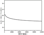
图7为双层交联PVA的电容-频率曲线。Figure 7 is the capacitance-frequency curve of double-layer cross-linked PVA.
图8为交联PVP、交联PVA的AFM图像。Fig. 8 is an AFM image of cross-linked PVP and cross-linked PVA.
图9为交联PVP、交联PVA的漏电曲线。Figure 9 is the leakage curves of cross-linked PVP and cross-linked PVA.
图10为交联PVP、交联PVA的电容-频率曲线。Figure 10 is the capacitance-frequency curve of cross-linked PVP and cross-linked PVA.
图11为双层交联介电层的并五苯底栅顶结构有机场效应晶体管的转移曲线。Fig. 11 is a transfer curve of a pentacene bottom-gate top-structure organic field-effect transistor with a double-layer cross-linked dielectric layer.
图12为双层交联介电层的并五苯底栅顶结构有机场效应晶体管的输出曲线。Fig. 12 is an output curve of a pentacene bottom-gate top-structure organic field-effect transistor with a double-layer cross-linked dielectric layer.
图13为双层交联介电层的PTCDI-C13底栅顶结构有机场效应晶体管的转移曲线。Fig. 13 is a transfer curve of a PTCDI-C13 bottom-gate top-structure organic field-effect transistor with a double-layer cross-linked dielectric layer.
图14为双层交联介电层的PTCDI-C13底栅顶结构有机场效应晶体管的输出曲线。Fig. 14 is the output curve of the PTCDI-C13 bottom-gate top-structure organic field-effect transistor with double-layer cross-linked dielectric layer.
图15为双层交联介电层的并五苯顶栅底结构有机场效应晶体管的转移曲线。Fig. 15 is a transfer curve of a pentacene top-gate-bottom structure organic field effect transistor with a double-layer cross-linked dielectric layer.
图16为双层交联介电层的并五苯顶栅底结构有机场效应晶体管的输出曲线。Fig. 16 is an output curve of a pentacene top-gate-bottom organic field-effect transistor with a double-layer cross-linked dielectric layer.
图17为双层交联介电层的并五苯底栅顶结构柔性有机场效应晶体管的转移曲线。Fig. 17 is a transfer curve of a pentacene bottom-gate top-structure flexible organic field-effect transistor with a double-layer cross-linked dielectric layer.
图18为双层交联介电层的并五苯顶栅底结构柔性有机场效应晶体管的输出曲线。Fig. 18 is an output curve of a pentacene top-gate-bottom structure flexible organic field-effect transistor with a double-layer cross-linked dielectric layer.
图中标记说明:1-第一层交联介电层;2-第二层交联介电层;3-第三层交联介电层;4-有机半导体层。Explanation of marks in the figure: 1-first cross-linked dielectric layer; 2-second cross-linked dielectric layer; 3-third cross-linked dielectric layer; 4-organic semiconductor layer.
具体实施方式detailed description
本发明提供了一种多层交联介电层,该多层交联介电层是在柔性衬底/电极上旋涂两层或两层以上交联聚合物;所述交联聚合物为交联PVA(聚乙烯醇)、PVP(聚(4-乙烯基苯酚))、PMMA(聚甲基丙烯酸甲酯)、PS(聚苯乙烯)、CYTOP(含氟树脂材料)、CEP(氰乙基支链淀粉)有机聚合物中的一种。The invention provides a multi-layer cross-linked dielectric layer, which is spin-coated with two or more layers of cross-linked polymers on a flexible substrate/electrode; the cross-linked polymers are Cross-linked PVA (polyvinyl alcohol), PVP (poly(4-vinylphenol)), PMMA (polymethyl methacrylate), PS (polystyrene), CYTOP (fluorine-containing resin material), CEP (cyanoethyl methacrylate) One of the organic polymers based on amylopectin.
PVA使用四乙氧基硅烷(TEOS)、四乙氧基硅烷(TEOS)与氯丙基硅氧烷(CPS)混合物、N,N-亚甲基双丙烯酰胺(MBA)、重铬酸铵(AD)或戊二醛(GD)作为交联剂。PVA uses tetraethoxysilane (TEOS), mixture of tetraethoxysilane (TEOS) and chloropropylsiloxane (CPS), N,N-methylenebisacrylamide (MBA), ammonium dichromate ( AD) or glutaraldehyde (GD) as cross-linking agent.
PVP使用X3Si-R-SiX3(R=-C6H12-、-C12H24-、O,X=Cl、OAc、NMe2、PVP uses X 3 Si-R-SiX 3 (R=-C 6 H 12 -, -C 12 H 24 -, O, X=Cl, OAc, NMe 2 ,
OMe、OAc)、HDA(4,4-(六氟异丙烯)二酞酸酐)、EDA(乙二胺四乙酸二酐)或BCD(二苯甲酮-3,3',4,4'-四羧酸二酐)作为交联剂。OMe, OAc), HDA (4,4-(hexafluoroisopropylene) diphthalic anhydride), EDA (ethylenediaminetetraacetic dianhydride) or BCD (benzophenone-3,3',4,4'- tetracarboxylic dianhydride) as a crosslinking agent.
PMMA、PS和CYTOP均使用C6-Si(1,6-双(三氯硅基)己烷)作为交联剂。PMMA, PS and CYTOP all use C 6 -Si(1,6-bis(trichlorosilyl)hexane) as crosslinking agent.
CEP使用EDT(乙二胺四乙酸二酐)或SCL(辛二酰氯)作为交联剂。CEP uses EDT (ethylenediaminetetraacetic dianhydride) or SCL (suberoyl chloride) as a crosslinking agent.
具体PVA、TEOS、TEOS和CPS的混合物、MBA、AD、GD、PVP、X3Si-R-SiX3、HDA、EDA、BCD、PMMA、PS、CYTOP、C6-Si、CEP、EDT和SCL的分子结构如表1所示。Specific PVA, TEOS, mixtures of TEOS and CPS, MBA, AD, GD, PVP, X 3 Si-R-SiX 3 , HDA, EDA, BCD, PMMA, PS, CYTOP, C 6 -Si, CEP, EDT and SCL The molecular structure is shown in Table 1.
为了更好地了解本发明的目的、结构及功能,下面结合附图,对本发明日出的一种多层交联介电层及其制备方法和应用做进一步详细的描述。In order to better understand the purpose, structure and function of the present invention, a multi-layer cross-linked dielectric layer of the present invention, its preparation method and application will be further described in detail below in conjunction with the accompanying drawings.
实施例1Example 1
双层交联介电层的制备方法,包括以下步骤:A method for preparing a double-layer cross-linked dielectric layer, comprising the following steps:
(1)在柔性衬底/电极上旋涂交联聚合物C-PVA,80℃退火30分钟,得到第一层交联介电层1,所述交联聚合物C-PVA为交联的PVA聚合物薄膜;(1) Spin-coat the cross-linked polymer C-PVA on the flexible substrate/electrode, and anneal at 80° C. for 30 minutes to obtain the first layer of cross-linked
(2)在步骤(1)中所得到的第一层交联介电层1上旋涂第二层交联聚合物C-PVA,80℃退火30分钟得到第二层交联介电层2,至此,得到双层交联介电层,如图1所示。图5示出了双层交联PVA的AFM图像、图6示出了双层交联PVA的漏电曲线、双层交联PVA的电容-频率曲线如图7所示;(2) Spin-coat the second layer of cross-linked polymer C-PVA on the first layer of cross-linked
其中:交联的PVA聚合物薄膜(即交联聚合物C-PVA)的制备方法如下:Wherein: the preparation method of the cross-linked PVA polymer film (i.e. cross-linked polymer C-PVA) is as follows:
步骤S1、首先配制20mg/ml PVA水溶液,采用体积比为1:1的四乙氧基硅烷和氯丙基硅氧烷的混合物作为交联剂,然后将交联剂与PVA水溶液混合,获得待加工的混合物溶液;Step S1, first prepare a 20mg/ml PVA aqueous solution, use a mixture of tetraethoxysilane and chloropropylsiloxane with a volume ratio of 1:1 as a crosslinking agent, and then mix the crosslinking agent with the PVA aqueous solution to obtain the Processed mixture solutions;
步骤S2、在柔性衬底/电极上旋涂一层上述混合溶液,然后在高温下退火,形成交联的PVA聚合物薄膜(交联聚合物C-PVA)。Step S2, spin coating a layer of the above mixed solution on the flexible substrate/electrode, and then annealing at high temperature to form a cross-linked PVA polymer film (cross-linked polymer C-PVA).
实施例2Example 2
双层交联介电层的制备方法,包括以下步骤:A method for preparing a double-layer cross-linked dielectric layer, comprising the following steps:
(1)配制20mg/ml的PVP溶液,并以重量比10:1的量加入交联剂HDA,并加入催化剂三乙胺,搅拌均匀,得到备用混合溶液;(1) Prepare a 20 mg/ml PVP solution, add the crosslinking agent HDA in a weight ratio of 10:1, and add the catalyst triethylamine, stir evenly to obtain a standby mixed solution;
(2)在柔性衬底/电极上旋涂上述混合溶液,100℃退火2小时,获得交联的PVP聚合物薄膜(即交联聚合物C-PVP),即第一层交联介电层1;(2) Spin-coat the above mixed solution on the flexible substrate/electrode, and anneal at 100°C for 2 hours to obtain a cross-linked PVP polymer film (ie, cross-linked polymer C-PVP), which is the first layer of cross-linked
(3)在步骤(1)中所得到的第一层交联介电层1上旋涂第二层交联聚合物C-PVA,80℃退火30分钟,得到第二层交联介电层2,至此,得到了双层交联介电层,如图1所示。介电层AFM图像、漏电曲线和电容-频率曲线,详见图8、图9和图10。(3) Spin-coat the second layer of cross-linked polymer C-PVA on the first layer of cross-linked
实施例3Example 3
三层交联介电层的制备方法,包括以下步骤:The preparation method of three-layer crosslinked dielectric layer comprises the following steps:
(1)在柔性衬底/电极上旋涂交联聚合物C-PVP,100℃退火2小时,得到第一层交联介电层1,其中交联聚合物C-PVP的制备过程同实施例2;(1) Spin-coat the cross-linked polymer C-PVP on the flexible substrate/electrode, and anneal at 100°C for 2 hours to obtain the first layer of cross-linked
(2)在步骤(1)中所得到的第一层交联介电层1上旋涂第二层交联聚合物C-PVA,80℃退火30分钟,得到第二层交联介电层2,得到了双层交联介电层,其中:交联聚合物C-PVA的制备过程同实施例1;(2) Spin-coat the second layer of cross-linked polymer C-PVA on the first layer of cross-linked
(3)在步骤(2)中所得到的双层交联介电层上旋涂第三层交联聚合物薄膜C-PVA,80℃退火30分钟,得到第三层交联介电层3,至此,得到三层交联聚合物薄膜,如图2所示,交联聚合物薄膜C-PVA的制备过程同实施例1。(3) Spin-coat the third layer of cross-linked polymer film C-PVA on the double-layer cross-linked dielectric layer obtained in step (2), and anneal at 80° C. for 30 minutes to obtain the third layer of cross-linked
实施例4Example 4
制备半导体层为并五苯底栅顶结构的有机场效应晶体管过程为:The process of preparing an organic field-effect transistor with a pentacene bottom-gate-top structure as a semiconductor layer is as follows:
(1)在双层交联介电层上,真空蒸镀并五苯半导体层,即图3中的有机半导体层4;(1) On the double-layer cross-linked dielectric layer, vacuum evaporate the pentacene semiconductor layer, i.e. the
(2)在步骤(1)中得到的半导体层的基础上,蒸镀氧化钼改善接触,再蒸镀Ag作为源漏电极,制备有机场效应晶体管,器件结构如图3所示。制备出的有机场效应晶体管的转移曲线如图11所示,输出曲线如图12所示。得到的迁移率为5.9cm2/vs,阈值电压为-1.1V。(2) On the basis of the semiconductor layer obtained in step (1), vapor-deposit molybdenum oxide to improve contact, and then vapor-deposit Ag as source and drain electrodes to prepare an organic field effect transistor. The device structure is shown in Figure 3. The transfer curve of the prepared organic field effect transistor is shown in FIG. 11 , and the output curve is shown in FIG. 12 . The obtained mobility was 5.9 cm 2 /vs, and the threshold voltage was -1.1V.
实施例5Example 5
制备半导体层为PTCDI-C13(N,N’-二(十三烷基)苝-3,4,9,10-四羧二酰亚胺)的底栅顶接触的有机场效应晶体管的过程如下:The process of preparing a bottom-gate top-contact organic field-effect transistor whose semiconductor layer is PTCDI-C13 (N,N'-bis(tridecyl)perylene-3,4,9,10-tetracarboxydiimide) is as follows :
(1)在衬底上,真空蒸镀Au源漏电极;(1) On the substrate, Au source and drain electrodes are vacuum evaporated;
(2)在步骤(1)中得到的源漏电极的基础上,蒸镀有机半导体PTCDI-C13,即图4中的有机半导体层4,在旋涂双层交联介电层作为介电层;(2) On the basis of the source-drain electrodes obtained in step (1), evaporate the organic semiconductor PTCDI-C13, that is, the
(3)在介电层表面蒸镀Au作为栅极,器件结构如图4所示。制备出的有机场效应晶体管转移曲线如图13所示,输出曲线如图14所示。迁移率为1.3cm2/vs,阈值电压为1.5V。(3) Au is vapor-deposited on the surface of the dielectric layer as a gate, and the device structure is shown in FIG. 4 . The transfer curve of the prepared organic field effect transistor is shown in FIG. 13 , and the output curve is shown in FIG. 14 . The mobility is 1.3cm 2 /vs, and the threshold voltage is 1.5V.
实施例6Example 6
制备半导体层为并五苯的顶栅底接触的有机场效应晶体管的过程如下:The process of preparing the organic field effect transistor with the top gate and bottom contact of pentacene as the semiconductor layer is as follows:
(1)在衬底上,真空蒸镀Au源漏电极;(1) On the substrate, Au source and drain electrodes are vacuum evaporated;
(2)在步骤(1)中得到的源漏电极的基础上,蒸镀有机半导体并五苯,即图4中的有机半导体层4,再旋涂双层交联介电层作为介电层;(2) On the basis of the source-drain electrodes obtained in step (1), evaporate the organic semiconductor pentacene, that is, the
(3)在介电层表面蒸镀Au作为栅极,器件结构如图4所示。制备出的有机场效应晶体管转移曲线如图15所示,输出曲线如图16所示。迁移率为26.2cm2/vs,阈值电压为-1.6V。(3) Au is vapor-deposited on the surface of the dielectric layer as a gate, and the device structure is shown in FIG. 4 . The transfer curve of the prepared organic field effect transistor is shown in FIG. 15 , and the output curve is shown in FIG. 16 . The mobility is 26.2cm 2 /vs, and the threshold voltage is -1.6V.
实施例7Example 7
制备半导体层为并五苯的柔性有机场效应晶体管的过程如下:The process of preparing a flexible organic field effect transistor whose semiconductor layer is pentacene is as follows:
(1)在柔性衬底上真空蒸镀Ag电极;(1) Vacuum evaporation of Ag electrodes on flexible substrates;
(2)在Ag电极上旋涂双层交联介电层上,并真空蒸镀并五苯半导体层;(2) Spin coating on the Ag electrode on the double-layer cross-linked dielectric layer, and vacuum-deposit the pentacene semiconductor layer;
(3)在步骤(2)中得到的半导体层的基础上,蒸镀氧化钼改善接触,在蒸镀Ag作为源漏电极,制备有机场效应晶体管,器件结构如图3所示。制备出的有机场效应晶体管转移曲线如图17所示,输出曲线如图18所示。迁移率为10.7cm2/vs,阈值电压为-1.2V。(3) On the basis of the semiconductor layer obtained in step (2), vapor-deposit molybdenum oxide to improve contact, and vapor-deposit Ag as source and drain electrodes to prepare an organic field effect transistor. The device structure is shown in Figure 3. The transfer curve of the prepared organic field effect transistor is shown in FIG. 17 , and the output curve is shown in FIG. 18 . The mobility is 10.7cm 2 /vs, and the threshold voltage is -1.2V.
实施例8Example 8
制备半导体层为NTDA-C6(2,7-二己基苯并【lmn】【3,8】菲咯啉-1,3,6,8(2H,7H)-四酮)底栅顶结构的有机场效应晶体管的过程如下:The semiconductor layer was prepared as NTDA-C 6 (2,7-dihexylbenzo[lmn][3,8]phenanthroline-1,3,6,8(2H,7H)-tetraketone) bottom gate top structure The process of organic field effect transistor is as follows:
(1)在双层交联介电层上,旋涂NTDA-C6半导体层。(1) On the double-layer cross-linked dielectric layer, spin-coat the NTDA-C 6 semiconductor layer.
(2)在步骤(1)中得到的半导体层的基础上,蒸镀Ag作为源漏电极,制备有机场效应晶体管,器件结构如图3所示。(2) On the basis of the semiconductor layer obtained in step (1), Ag is evaporated as source and drain electrodes to prepare an organic field effect transistor, and the device structure is shown in FIG. 3 .
可以理解,本发明是通过一些实施例进行描述的,本领域技术人员知悉的,在不脱离本发明的精神和范围的情况下,可以对这些特征和实施例进行各种改变或等效替换。另外,在本发明的教导下,可以对这些特征和实施例进行修改以适应具体的情况及材料而不会脱离本发明的精神和范围。因此,本发明不受此处所公开的具体实施例的限制,所有落入本申请的权利要求范围内的实施例都属于本发明所保护的范围内。It can be understood that the present invention is described through some embodiments, and those skilled in the art know that various changes or equivalent substitutions can be made to these features and embodiments without departing from the spirit and scope of the present invention. In addition, the features and examples may be modified to adapt a particular situation and material to the teachings of the invention without departing from the spirit and scope of the invention. Therefore, the present invention is not limited by the specific embodiments disclosed here, and all embodiments falling within the scope of the claims of the present application belong to the protection scope of the present invention.
表1Table 1


Claims (10)
Priority Applications (1)
| Application Number | Priority Date | Filing Date | Title |
|---|---|---|---|
| CN202211107718.1A CN115440887A (en) | 2022-09-13 | 2022-09-13 | Multilayer cross-linked dielectric layer and preparation method and application thereof |
Applications Claiming Priority (1)
| Application Number | Priority Date | Filing Date | Title |
|---|---|---|---|
| CN202211107718.1A CN115440887A (en) | 2022-09-13 | 2022-09-13 | Multilayer cross-linked dielectric layer and preparation method and application thereof |
Publications (1)
| Publication Number | Publication Date |
|---|---|
| CN115440887A true CN115440887A (en) | 2022-12-06 |
Family
ID=84247474
Family Applications (1)
| Application Number | Title | Priority Date | Filing Date |
|---|---|---|---|
| CN202211107718.1A Pending CN115440887A (en) | 2022-09-13 | 2022-09-13 | Multilayer cross-linked dielectric layer and preparation method and application thereof |
Country Status (1)
| Country | Link |
|---|---|
| CN (1) | CN115440887A (en) |
Citations (3)
| Publication number | Priority date | Publication date | Assignee | Title |
|---|---|---|---|---|
| US20080161464A1 (en) * | 2006-06-28 | 2008-07-03 | Marks Tobin J | Crosslinked polymeric dielectric materials and methods of manufacturing and use thereof |
| CN105336860A (en) * | 2015-11-09 | 2016-02-17 | 南京邮电大学 | Flexible low-voltage organic field effect transistor and manufacturing method thereof |
| CN113540254A (en) * | 2021-06-08 | 2021-10-22 | 华南师范大学 | Neodymium-doped zirconia thin film transistor and preparation method and application thereof |
-
2022
- 2022-09-13 CN CN202211107718.1A patent/CN115440887A/en active Pending
Patent Citations (3)
| Publication number | Priority date | Publication date | Assignee | Title |
|---|---|---|---|---|
| US20080161464A1 (en) * | 2006-06-28 | 2008-07-03 | Marks Tobin J | Crosslinked polymeric dielectric materials and methods of manufacturing and use thereof |
| CN105336860A (en) * | 2015-11-09 | 2016-02-17 | 南京邮电大学 | Flexible low-voltage organic field effect transistor and manufacturing method thereof |
| CN113540254A (en) * | 2021-06-08 | 2021-10-22 | 华南师范大学 | Neodymium-doped zirconia thin film transistor and preparation method and application thereof |
Similar Documents
| Publication | Publication Date | Title |
|---|---|---|
| Yang et al. | Low-voltage organic single-crystal field-effect transistor with steep subthreshold slope | |
| Duan et al. | Low-power-consumption organic field-effect transistors | |
| CN101179108A (en) | Non-volatile organic thin film transistor memory based on floating gate structure and its manufacturing method | |
| CN113161486B (en) | P-type organic thin film transistor based on molybdenum trioxide contact doping and preparation method | |
| CN105336860A (en) | Flexible low-voltage organic field effect transistor and manufacturing method thereof | |
| CN105810820A (en) | Porous structure organic field effect transistor photosensitive memory and preparation method thereof | |
| CN1767158A (en) | The method for preparing thin-film transistor | |
| CN108011042A (en) | Double-deck active layer thin film transistor (TFT) and preparation method | |
| KR20160112030A (en) | Thin-film transistor having dual gate electrode | |
| CN107611262B (en) | Flexible dielectric film and organic field effect transistor prepared from same | |
| CN108831996A (en) | A three-layer heterojunction organic field effect transistor memory and its preparation method | |
| CN101257092A (en) | A kind of organic thin film transistor and its preparation method | |
| Xiang et al. | Improving mobility and stability of organic field-effect transistors by employing a tetratetracontane modifying PMMA dielectric | |
| CN1622362A (en) | Organic thin film transistor comprising buffer layer | |
| Wang et al. | Research progress on crosslinked polymer-based dielectrics for thin film capacitors | |
| CN103022077B (en) | A kind of OLED device of oxycompound thin-film transistor | |
| KR20080043239A (en) | A method of forming an organic ferroelectric film, a method of manufacturing a memory element, a storage device, and an electronic device | |
| CN114583050A (en) | Stretchable organic electrochemical transistor and preparation method thereof | |
| CN106531886A (en) | Quantum dot-based organic field effect transistor photosensitive memory and preparation method thereof | |
| CN105470389B (en) | Flexible organic field effect transistor with three-dimensional structure | |
| CN112051316A (en) | Ammonia gas sensor based on organic thin film transistor and preparation method thereof | |
| CN101257093B (en) | A kind of organic thin film transistor and its preparation method | |
| CN115440887A (en) | Multilayer cross-linked dielectric layer and preparation method and application thereof | |
| CN106981573B (en) | A kind of organic field effect transistor memory with self-blocking layer structure and preparation method thereof | |
| CN108878649A (en) | Self-supporting ultrathin flexible high-performance organic film FET and preparation method thereof |
Legal Events
| Date | Code | Title | Description |
|---|---|---|---|
| PB01 | Publication | ||
| PB01 | Publication | ||
| SE01 | Entry into force of request for substantive examination | ||
| SE01 | Entry into force of request for substantive examination | ||
| RJ01 | Rejection of invention patent application after publication | ||
| RJ01 | Rejection of invention patent application after publication |
Application publication date: 20221206 |