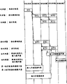
First embodiment
Fig. 1 is the block scheme of the structure of the signal conditioning package of the displaying first embodiment of the present invention.This signal conditioning package is to be made of processor 101, coprocessor 102 and storer 103 that data processing unit input bus 124, data processing unit output bus 125, instruction supply bus 126, data bus 127, data bus 128, flag data bus 130 and flag data bus 131 interconnect as can be seen, as shown in FIG..
Processor 101 is made up of demoder 104, control circuit 105, general-purpose register 106, sign storage register 108, order register 112, microinstruction register 113, data latches 114, register write buffer 116, memory write impact damper 117, coprocessor data latches 118, condition managing unit 129, pipeline latch 143, driver 121-123 and 132-135, first data processing unit 140 and second data processing unit 141.The five-stage pipelined process that processor 101 utilizations are made of instruction fetch phase, instruction decode stage, first execute phase, second execute phase and write phase is come the instruction in the processing memory 103.Comprise the instruction (after this being called " processor instruction ") of processor 101 and the instruction (after this being called " coprocessor instruction ") of coprocessor 102 in the instruction in the storer 103.When processor 101 during at coprocessor instruction of instruction decode stage decoding, it retrieves the specified source data of operand in the instruction and these data is supplied with coprocessor 102 from general-purpose register 106, coprocessor 102 then is stored in its result of calculation in the general-purpose register 106.Here processor 101 is set at 32 bit processors, unless and offer some clarification on, highway width is set at 32.
Coprocessor 102 is made up of demoder 109, control circuit 110, order register 119, microinstruction register 120, first to the 3rd pipeline latch 160-162, first to fourth coprocessor processing unit 150-153 and first to the 3rd pipeline latch 160-162.Coprocessor 102 is one of a plurality of coprocessors, its is carried out such as multiplication and division, sum of products, bit field calculatings, character string calculatings, saturated calculating, the coprocessor processes such as calculating, context handoff procedure and filter process of lining up, and comprises and depend on that use can support other coprocessor of desired various calculating.In the present embodiment, desired calculating kind is set at multiplication, and this is to utilize the pipelined process that is made of an instruction decode stage and first to fourth execute phase to carry out.Here, the example of the coprocessor instruction of expression multiplication is illustrated among Fig. 2.In the figure, " MULQ Dm Dn " expression source-register Dm (32 integers that have extracode) multiplies each other with source-register Dn (32 integers that have extracode), low 32 with result's (64 figure place) are stored among the destination register Dn, and among high 32 the multiply register MR that are stored in the general-purpose register 106 with result's (64 figure place).In same figure, " MULQ imm 8, Dn " is illustrated in and expands 32 given place values of 8 immediate datas and the multiplication of source-register Dn (32 integers that have extracode) on the data of application code, and the result is stored among Dn and the MR." MULQ imm 16, Dn " and " MULQ imm 32, Dn " are too.
Storage is made of processor and coprocessor instruction in the storer 103 program and processor 101 and coprocessor 102 employed data.
Demoder 104 is decoded in instruction decode stage and is supplied with processor instruction and the coprocessor instruction that bus 126 and instruction registers 112 take out from storer 103 by instruction, and the output micro-order is for the instruction that realizes being taken out.More specifically, decoding during a coprocessor instruction (for example in Fig. 2, when the Gao Siwei of order code is " FH "), (1) micro-order that reads by the indicated source-register of the operand in the coprocessor instruction of demoder 104 issues, article (2) one, will read the micro-order of data latching in coprocessor data latches 118 from source-register, flag data in (3) the one regulations sign storage registers 108 outputs to micro-order on the flag data bus 130 by driver 134, article (4) one, to the micro-order of first data processing unit 140 and second data processing unit 141 indication NOP (blank operation), article (5) one, the result of calculation with coprocessor 102 is stored in by the micro-order in the operand purpose of indicating register, and (6) one will be stored in the micro-order that indicates in the storage register 108 from the flag data of coprocessor 102 by driver 135.In these micro-orders, three of fronts are directly not output to control circuit 105 by microinstruction register 113, and remaining micro-order then outputs to control circuit 105 by microinstruction register 113.Thereby, in instruction decode stage, at first carry out first three bar micro-order.Should point out, shown in (1) to (6), also can be arranged to make a micro-order to constitute above these micro-orders can be arranged to by some micro-orders.
Demoder 104 also is provided with a continuity number according to the type of coprocessor instruction, and it is outputed to condition managing unit 129.Here, the continuity numerical table shows execute phase number poor of the execute phase number of processor 101 and coprocessor 102.Thereby this must be added in the number of idle condition (NOP) execute phase on the processor 101 term of execution of being illustrated in the instruction of coprocessor.In the present embodiment, the execute phase number of coprocessor 102 and the execute phase number of processor 101 are respectively 4 and 2, therefore work as demoder 104 and determine that decoded results are that coprocessor instruction is that multiplying order is (for the example among Fig. 2, when the most-significant byte in the order code is F6H, F9H and FBH) time, demoder 104 just will continue number and be set on 2.
Control circuit 105 in the processor 101 will be directly from demoder 104 inputs or convert various control signals to from the micro-orders of demoder 104 inputs indirectly by microinstruction register 113, and as the circuit of control pipeline processes.When having imported above-mentioned instruction (1) as the decoded result of a coprocessor instruction, (2) with (3), control circuit 105 outputs be used for the indicated register of general-purpose register 106 a read signal, be used for starting a control signal of driver 122, a control signal that is used to make coprocessor data latches 118 to carry out a control signal that latchs and be used for starting driver 134 at the decode phase of the execute phase front of the instruction of being taken out.In an identical manner, when input instruction (5) and (6), one of control circuit 105 output is used to make general-purpose register 106 to carry out the control signal that latchs, and is used for by the write signal of the register of general-purpose register 106 appointments and a control signal that is used to start driver 135.
General-purpose register 106 is kept the register D0-D3 of 32 bit data and is kept high 32 the multiply register MR of product to constitute by each.
Order register 112 controlled circuit 105 controls output to demoder 104 so that supply with bus 126 with one by instruction from the instruction that storer 103 takes out.When switching to instruction decode stage from the instruction fetch phase, this output just switches to next bar instruction at every turn.
The various signs of sign storage register 108 storage representation processor states, second data processing unit 141 of processor 101 generated sign and the 4th coprocessor processing unit 153 of coprocessor 102 generates the sign both and reflects by the control that control circuit 105 is carried out.
Microinstruction register 113 outputs to control circuit 105 according to the micro-order of the control self-demarking code in the future device 104 of control circuit 105.When instruction decode stage switched to for first execute phase, this output just switched to next bar instruction (or instruction group) at every turn.
Data latches 114 will output to first data processing unit 140 according to the control of control circuit 105 from the operand data that general-purpose register 106 reads by data processing unit input bus 124.When instruction decode stage switched to for first execute phase, this output just switched to next bar instruction at every turn.
Register write buffer 116 will output to general-purpose register 106 from the data of data processing unit output bus 125 after finishing for second execute phase according to being controlled at of control circuit 105.
Memory write impact damper 117 outputs to data on the data bus 128 from data processing unit output bus 125 after finishing for second execute phase according to being controlled at of control circuit 105.
Coprocessor data latches 118 according to the control of control circuit 105, outputs to coprocessor 102 by data processing unit input bus 124 with register data when switching to for first execute phase from instruction decode stage.
Driver 121 has a door of opening according to the control of control circuit 105, and is the driver that is used for by data bus 127 data of transmission memory 103 on data processing unit input bus 124.
Driver 122 has a door of opening according to the control of control circuit 105, and is the driver that is used for transmitting on data processing unit input bus 124 from the data of general-purpose register 106.
Driver 123 has a door of opening according to the control of control circuit 105, and is the driver that is used for transmitting on data processing unit output bus 125 from the data of second data processing unit 141.
Data processing unit input bus 124 is used for giving first data processing unit 140 and coprocessor data latches 118 with the general-purpose register 106 of from processor 101 inside and from the data transmission of storer 103, and data are transferred to the first coprocessor processing unit 150 coprocessor 102 from coprocessor data latches 118.Should be specifically noted that data processing unit input bus 124 is given the first coprocessor processing unit 150 in the coprocessor 102 by coprocessor data latches 118 with the data transmission in the general-purpose register 106 of processor 101.In the present embodiment, this bus has two 32 width.
Data processing unit output bus 125 is used for execution result with second data processing unit 141 of from processor 101 and the 4th coprocessor processing unit 153 in the coprocessor 102 and is transferred to register write buffer 116 and memory write impact damper 117 in the processor 101.Notice that data processing unit output bus 125 is to be used for the bus that the 4th coprocessor processing unit 153 data processed with second data processing unit 141 of processor 101 and coprocessor 102 are transferred to general-purpose register 106 and storer 103.In the present embodiment, this bus has two 32 bit widths.
It is that the instruction that is used for being stored in storer 103 is transferred to the order register 112 in the processor 101 and the bus of the order register 119 in the coprocessor 102 that bus 126 is supplied with in instruction.
Data bus 127 transmits the data that are stored in the storer 103 by driver 121 on data processing unit input bus 124.
Data bus 128 will be given storer 103 from the data transmission of data processing unit output bus 125 by memory write impact damper 117.
All states of the flow line stage of condition managing unit 129 management processors 101, and whether management advances in cycle of current generation back next process or whether continues the current generation.More specifically, the flag information of the state of condition managing unit 129 storage representation flow line stages.This flag information represents to indicate " the next stage executing state " of next process in the cycle that advances to the current generation back or indication " the current generation continuity state " in the following one-period continuous current generation of relaying.When processor instruction of demoder 104 decodings, to carry out for the instruction of in two stages that constitute by first execute phase and second execute phase, finishing, this flag information shows " next stage executing state ".When coprocessor instruction of demoder 104 decoding, demoder 104 notify status administrative units 129 continuity numbers, in next execute phase again, flag information shows that " current generation continuity state " equals some stages of this continuity number.For example, when the continuity that has notice several 2 the time, flag information is showing that " current generation continuity state " shows " next stage executing state " before in first execute phase, and " current generation continuity state " shows in second execute phase " next stage executing state " then then.Do like this, the execute phase number of condition managing unit 129 management processors 101 makes it to equate with the execute phase number of coprocessor 102.
Flag data bus 130 is the buses that are used for the flag data of sign storage register 108 is transferred to coprocessor 102.The bit width of this bus can be set according to the number of sign.
Flag data bus 131 is the buses that are used for the flag data that the 4th coprocessor processing unit 153 was handled is transferred to the sign storage register 108 of processor 101.The bit width of this bus can be set according to the number of sign.
Driver 132 has a door of opening according to the control of control circuit 105, and is the driver that is used for flag data is transferred to from sign storage register 108 first data processing unit 140.
Driver 133 has a door of opening according to the control of control circuit 105, and is the driver that is used for flag data is transferred to from second data processing unit 141 sign storage register 108.
Driver 134 has a door of opening according to the control of control circuit 105, and is the driver that is used for flag data is transferred to from sign storage register 108 coprocessor 102.
Driver 135 has a door of opening according to the control of control circuit 105, and is the driver that is used for flag data is transferred to from coprocessor 102 sign storage register 108.
First data processing unit 140 according to control circuit 105 be controlled at first execute phase in the processor 101 during carry out data processing.When coprocessor instruction of demoder 104 decoding, first data processing unit 140 is set at idle condition (NOP) according to the control of control circuit 105.
Second data processing unit 141 is carried out data processing during second execute phase of processor 101.When coprocessor instruction of demoder 104 decoding, second data processing unit 141 is set at idle condition (NOP) according to the control of control circuit 105.
When in execution pipeline control according to the control of control circuit 105, switched to for second execute phase and when first data processing unit 140 was transferred to second data processing unit 141, pipeline latch 143 was opened its latch from first execute phase.
As for the coprocessor among Fig. 1 102, during instruction decode stage, demoder 109 decodings are supplied with the instruction that bus 126 and instruction registers 112 take out from storer 103 by instruction.When decoded result was a coprocessor instruction, demoder 109 was just issued a micro-order and is realized by the calculating content shown in the OP sign indicating number of this coprocessor instruction.Should point out, there is no need to issue a micro-order and indicate the register that is used for reading and writing the operand data of coprocessor instruction.This be because operand register read carry out by processor 101 with write operation.
Control circuit 110 in the processor will convert various control signals to from the micro-order of demoder 109 input by microinstruction register 120, and as the circuit of the pipeline processes of control coprocessor 102.
Order register 119 will be supplied with bus 126 by instruction and export to demoder 109 from the instruction that storer 103 takes out.When switching to instruction decode stage from the instruction fetch phase, this output just switches to next bar instruction at every turn.
Microinstruction register 120 when switching to for first execute phase from instruction decode stage, outputs to control circuit 110 with micro-order from demoder 109 according to the control of the control circuit 110 in the execution pipeline control.When instruction decode stage switched to for first execute phase, this output just switched to next bar instruction (or instruction group) at every turn.
Data processing in first execute phase of the first coprocessor processing unit, 150 execution coprocessors 102.
Data processing in second execute phase of the second coprocessor processing unit, 151 execution coprocessors 102.
Data processing in the 3rd execute phase of the 3rd coprocessor processing unit 152 execution coprocessors 102.
Data processing in the 4th execute phase of the 4th coprocessor processing unit 153 execution coprocessors 102.
First pipeline latch 160, switching to for second execute phase and when the first coprocessor processing unit 150 is transferred to the second coprocessor processing unit 151, opening its latch from first execute phase according to the control of the control circuit 110 in the execution pipeline control.
Second pipeline latch 161, switching to for the 3rd execute phase and when the second coprocessor processing unit 151 is transferred to the 3rd coprocessor processing unit 152, opening its latch from second execute phase according to the control of the control circuit 110 in the execution pipeline control.
The 3rd pipeline latch 162, switching to for the 4th execute phase and when the 3rd coprocessor processing unit 152 is transferred to the 4th coprocessor processing unit 153, opening its latch from the 3rd execute phase according to the control of the control circuit 110 in the execution pipeline control.
Be the explanation of signal conditioning package of the first embodiment of the present invention of above-mentioned structure below.
Fig. 3 is the time diagram of the state of displaying pipeline processes, at this moment for coprocessor 102, handle the operation of the data of the general-purpose register 106 of from processor 101 and sign storage register 108, then with the result data storage in general-purpose register 106 and sign storage register 108.
In the figure, " IF1 " is the stage of a coprocessor instruction of processor 101 retrievals." OP1 " is the stage of a coprocessor instruction of processor 101 decodings." EXP1 " and " EXP2 " is respectively first and second execute phase (or NOP) of a coprocessor instruction in the processor 101." WB1 " writes the stage of the result of calculation of coprocessor 102 for processor 101." DE1 " is the stage of a coprocessor instruction of decoding of coprocessor 102." EXE1 ", " EXE2 ", " EXE3 " and " EXE4 " are respectively the first, second, third and the 4th execute phase of a coprocessor instruction in the coprocessor 102." NXT-IF " takes out the stage of an instruction of the instruction back that " IF1 " got for processor 101." NXT-DP " is the stage of next bar instruction of processor 101 decodings." NXT-EXP1 " and " NXT-EXP2 " are respectively first and second execute phase that next bar instructs in the processor 101.
In the time interval 1, storer 103 outputs to guiding processor 101 with an instruction and supplies with on the bus 126 with the instruction of coprocessor 102 in the instruction fetch phase of processor 101 (IF1).
Switch to the time interval 2 from the time interval 1, the control circuit 105 in the processor 101 advances to (DP1) and correspondingly opens the order register 112 of processor 101 from (IF1).In an identical manner, the control circuit 110 in the coprocessor 102 advances to the order register 119 that (DE1) also correspondingly opens coprocessor 102 from (IF1).
In the time interval 2, storer 103 outputs to guiding processor 101 with next bar instruction and supplies with on the bus 126 with the instruction of coprocessor 102 in the instruction fetch phase (NXT-IF1).
In instruction decode stage (DP1), after order register 112 was opened, the demoder 104 in the processor 101 received instruction, decoding instruction then.Then, control circuit 105 utilizes the micro-order of demoder 104 outputs, start driver 122 data in the general-purpose register 106 are placed on the data processing unit input bus 124, and startup driver 134 will indicate that the flag information in the storage register 108 is placed on the flag data bus 130.
In the instruction decode stage (DE1) of coprocessor 102, the demoder 109 in the coprocessor 102 receives instruction, this instruction of decoding then after order register 119 is opened.
From the time interval 2 to the time interval 3 the switching, the control circuit 105 in the processor 101 advances to (NXT-DP) and OPEN register 112 correspondingly from (NXT-IF).
Control circuit 105 in the processor 101 advances to from flow line stage (DP1) and to open microinstruction register 113, data latches 114 and coprocessor data latches 118 (EXP1).Similarly, the control in the coprocessor 110, system circuit 110 advances to from flow line stage (DE1) opens microinstruction register 120 (EXE1).In case opened microinstruction register 113, the control circuit 105 in the processor 101 receives the micro-order that demoder 104 is decoded in the instruction decode stage (DP1).Similarly, in case opened microinstruction register 120, the micro-order that the demoder 109 that the control circuit 110 in the coprocessor 102 receives coprocessor 102 in the instruction decode stage (DE1) is decoded.
In the time interval 3, behind OPEN register 112, the demoder 104 of processor 101 receives instruction, this instruction of decoding in the instruction decode stage (NXT-DP) of processor 101 then.
In first execute phase of processor 101 (EXP1), first data processing unit 140 in the processor 101 is not carried out data processing (NOP).
In first execute phase of coprocessor 102 (EXE1), the first coprocessor processing unit 150 in the coprocessor 102 is carried out data processing.
Switch to the time interval 4 from the time interval 3, open microinstruction register 113 flow line stage of the control circuit 105 of processor 101 from (NXT-DP) to (NXT-EXP) switches.Opened after the microinstruction register 113, the control circuit 105 of processor 101 just receives the micro-order that demoder 104 is decoded in (NXT-DP) instruction decode stage.
Flow line stage from (EXP1) to (EXP2) switched, the control circuit 105 of processor 101 was opened the pipeline latch 143 of processor 101.
Flow line stage from (EXE1) to (EXE2) switched, the control circuit 110 of coprocessor 102 was opened first pipeline latch 160 of coprocessor 102.
In the time interval 4, first data processing of next bar instruction in first execution phase (NXT-EXP1) of first data processing unit, the 140 execution processors 101 in the processor 101.
In second execution phase of processor 101 (EXP2), second data processing unit 141 is not carried out data processing (NOP).
Condition managing unit 129 from next stage executing state change to current state continuity state, and transmit a current generation continuity signal and give control circuit 105.
In second execution phase of coprocessor 102 (EXE2), the second coprocessor processing unit 151 of coprocessor 102 is carried out data processing.
Switch to the time interval 5 from the time interval 4, because condition managing unit 129 sends current states continuity signals, the control circuit 105 in the processor 101 is not opened pipeline latch 143.Thereby the state of current generation is extended to next stage.
Then, switch to (EXE3) from flow line stage (EXE2), the control circuit 110 in the coprocessor 102 is opened second pipeline latch 161.
In the time interval 5, be 101 continuity first execution phases (NXT-EXP1) of processor, make first data processing unit 140 in the processor 101 continue first data processing of next instructions, as mentioned above.
Owing to continued the stage in second execution phase of processor 101 (EXP2), second data processing unit 141 in the processor 101 is not carried out data processing (NOP).
In the 3rd execution phase of coprocessor 102 (EXE3), the 3rd coprocessor processing unit 152 of coprocessor 102 is carried out data processing.
Switch to the time interval 6 from the time interval 5, because condition managing unit 129 sends a current generation continuity signal (NOP), the control circuit 105 in the processor 101 is not opened pipeline latch 143.
Then in coprocessor 102, switch to (EXE4) from flow line stage (EXE3), control circuit 110 is opened the 3rd pipeline latch 162.
In the time interval 6, be 101 continuity first execution phases (NXT-EXP1) of processor, make that first data processing unit 140 in the processor 101 continues first data processing that next bar instruction is carried out, as mentioned above.
Owing to continued the stage in second execution phase of processor 101 (EXP2), second data processing unit 141 in the processor 101 is not carried out data processing (NOP).
By making second data processing unit 141 will be extended to 3 stages (EXP2) stage (in other words, this stage is prolonged two stages), before switching to " next stage executing state " from " current generation continuity state " and finishing to continue the current generation control circuit 105 that signal is transferred to processor 101, condition managing unit 129 makes the stage of processor 101 continue and time interval of continuity number equivalence.
In the 4th execution phase of coprocessor 102 (EXE4), the 4th coprocessor processing unit 153 of coprocessor 102 is carried out data processing and is therefore being exported result data on the data processing unit output bus 125 and output identification information on flag data bus 131.Then, the driver 154 that the control circuit 110 in the coprocessor 102 starts in the coprocessor 102 makes and exports on data processing unit output bus 125 through the 4th coprocessor processing unit 153 data processed.
Switch to the time interval 7 from the time interval 6, the control circuit 105 in the processor 101 is switching to the pipeline latch of opening (NXT-EXP2) in the processor 101 143 from flow line stage (NXT-EXP1).
Control circuit 105 in the processor 101 switches to from flow line stage (EXP2) and starts driver 135 (WB1), and feasible flag information from flag data bus 131 is transferred to sign storage register 108.
In the time interval 7, in second execution phase of processor 101 (NXT-EXP2), second data processing unit 141 is carried out second data processing that next instruction is carried out.
In the write phase (WB1) of processor 101, general-purpose register 106 receives from the data of data processing unit output bus 125 and stores this data.Similarly, coprocessor 102 sends to the flag information of processor 101 on the sign storage register 108 receiving flag data buss 131, and stores it.
In this way, coprocessor 102 can directly use the data in the general-purpose register 106 in calculating, thereby process can be accelerated by the shared time of memory transfer data, because this technology no longer needs to pass through memory transfer.Here can accelerate the quoting of sign in the sign storage register 108 of processor 101 in an identical manner.In addition, because the confusion in the pipeline processes of the data inequality in having avoided transmitting and processor 101 and coprocessor 102 can reduce the execution time.
Here, when not needing coprocessor 102, the data processing unit input bus 124 that is used for connection processing device 101 and coprocessor 102 and data processing unit output bus 125, be used for that storer 103 is connected part instruction on the coprocessor 102 and supply with bus 126, be used for connection processing device 101 to the flag data bus 130 of coprocessor 102 and be used to be connected coprocessor 102 and all can disconnect to the flag data bus 131 on the processor 101.
Simultaneously, when comparing, when the coprocessor deal with data, no longer need to send pending data to coprocessor, this means and to reduce the execution time by storer with relevant technical examples.
Moreover, in this first embodiment, demoder 104 in the processor 101 is determined the continuity number according to the type of coprocessor instruction, but also one of processor 101 usefulness may be calculated in the data processing unit that the end signal line be connected coprocessor 102 on any one, calculate end signal and just can continue by condition managing unit 129 done states by transmitting one.In addition, also coprocessor instruction itself can be arranged to comprise the information of the difference in the flow line stage between expression processor 101 and the coprocessor 102, thereby make demoder 104 will continue number notify status administrative unit 129 from the state of this information.
Here should point out, though native system can constitute processor 101 is connected on a plurality of dissimilar coprocessors 102, above-mentioned explanation is 101 of processors to be connected a situation on the coprocessor 102 describe.For processor 101 being connected a coprocessor that is used to carry out multiplication, be used to carry out on the coprocessor of the sum of products and be used to carry out a example on the coprocessor of division, then can between processor 101 and each coprocessor, be provided with by instruction and supply with five buses that bus 126, data processing unit input bus 124, data processing unit output bus 125, flag data bus 130 and flag data bus 131 constitute.In this case, the bit pattern that is necessary in the order code of coprocessor instruction divides each coprocessor of pairing unique pattern.This moment, processor 101 can be that any coprocessor of above-mentioned bus that utilizes is carried out supply and storage register data and sign in the identical mode of present embodiment just.Here, these coprocessors are only to be designed to when decoded result is represented to be used for coprocessor instruction of this specific coprocessor, just carry out coprocessor instruction with the same way as of the coprocessor in the present embodiment 102.
Simultaneously, present embodiment has been described the situation of processor 101 execution 2 stage pipelined process and coprocessor 102 execution 4 stage pipelined process, but this structure is not limited to these values.(1≤b) pipelined process and processor 101 are carried out the c stages (during the pipelined process of 1≤c≤b) when coprocessor 102 is carried out the b stages, can a condition managing unit be set on the stage at c, notify this condition managing unit continuity number b-c by demoder, and make the c stage continue the number of stages that execution equals to continue number.(c>b), then the continuity number can be set at zero when the execute phase of processor number is longer than coprocessor several.In this case, on the point of having finished c execute phase, processor is got result of calculation from coprocessor, and coprocessor then begins to export result of calculation from the point of having finished b execute phase, thereby till processor is finished c execute phase reception execution result.
Moreover, it is to be described as being connected on the input side of order register 112 of processor 101 and on the input side of the order register 119 of coprocessor 102 that bus 126 is supplied with in instruction, but an instruction that only input side of the order register 112 of processor 101 is connected on the storer 103 also may be set supply with bus, and with another bus the outgoing side of the order register 112 of processor 101 is connected on the input side of demoder 109 of coprocessor 102.In this way, can save order register 119, thereby the electric load of instruction supply bus is minimized.
When this signal conditioning package is when being made of a LSI, then as shown in Figure 11, the configuration of processor 101 can be divided into a control module unit that is made of demoder 104 and control circuit 105; An and data path unit that waits formation by first data processing unit 140, second data processing unit 141, data bus (bus 126 is supplied with in data processing unit input bus 124, data processing unit output bus 125, instruction).The configuration of coprocessor 102 also can be divided into a control module unit that is made of demoder 109 and control circuit 110 and a data path unit that is made of first to fourth coprocessor processing unit 150-153, data bus etc.In this configuration, always exist the correlativity of the bit slice (bit width) of the data bus in one side of configuration of data path unit, thereby because in this signal conditioning package, data bus is that processor and coprocessor are shared, can easily increase the new coprocessor that is used for dissimilar calculating, and need not consider whether coprocessor 102 exists.In this way, can be easily on a chip, realize having the signal conditioning package of a plurality of coprocessors of each tool difference in functionality.
Second embodiment
Fig. 4 is the block scheme of the structure of the signal conditioning package of the displaying second embodiment of the present invention.As can be seen, this signal conditioning package is made of processor 201, coprocessor 202, storer 203, preservation data storing buffer 232 and driver 259.Note with first embodiment in identical composed component given identical reference number and omitted their description, thereby following description focuses on the difference with first embodiment.
Among Fig. 4, processor 201 is to be arranged to carry out the 4 stage pipelined process that are made of an instruction fetch phase, instruction decode stage, execution phase and write phase, for convenience of explanation, only will regard as the execute phase by a stage and constitute.And the main difference of first embodiment is to relate to one of execution and is used for the move instruction that the general-purpose register 106 between processor 201 and coprocessor 202 transmits data, and relate to when interrupt procedure begins and to produce one to the replying after the coprocessor of notice, be branched off on these 2 of the interrupt procedures.As a result, also comprise interrupt request singal line 240, look-at-me line 241 and finish signal wire 242 in the structure.In the present embodiment, the data processing unit output bus 125 that is made of two 32 buses among first embodiment can only be made of 32 buses.
Coprocessor 202 is to be arranged to carry out the 4 stage pipelined process that are made of an instruction fetch phase, instruction decode stage, execution phase and write phase, only will regard as the execute phase for convenience of explanation by a stage to constitute.Be to relate to the execution of coprocessor move instruction with the main difference of first embodiment and relate to from processor 201 receive notice that interrupt procedures begin, in commission the way stop coprocessor instruction with preserve data and to processor 201 transmission expression ready states reply this some on.The result, this structure additionally comprises data processing unit input buffer 230, data processing unit output buffer 231, preservation data storing buffer 232 and the driver 250,251 and the 253-259 that center on them, and these preserve bus 243 with the data processing unit input buffer and the data processing unit output buffer returns bus 245 connections.
Coprocessor move instruction in the present embodiment comprises from the general-purpose register 106 of processor 201 inside to the data movement instruction of the data processing unit input buffer 230 of coprocessor 202 inside and the data movement instruction of the general-purpose register 106 of 201 inside from data processing unit output buffer 231 to processor.These are to represent such as the form shown in following, it specifies the source and the destination of move instruction (" MOVE " instruction), such as data processing unit input buffer 230 (breviary is ex_in BUF) and data processing unit output buffer 231 (breviary is ex_out BUF).
MOV Dn ex_in buf: data from register Dn to ex_in BUF
Transmit
MOV ex_ouf BUF, Dn: from ex_out BUF to register Dn's
Data transmit
In the present embodiment, coprocessor 202 is to be set to carry out coprocessor instruction that the appointment comprise 3 or more operand data calculates, calculates Dn such as three
*Dm+D1.When doing like this, send an operand data D1 in three calculating to coprocessor 202 with the coprocessor move instruction in advance.In an identical manner, when the result of calculation of three calculating is increased to a plurality of word length, send a part of result of calculation to processor 201 with move instruction.
Interrupt request singal line 240 in the processor 201 is sent to interrupt request the control circuit 205 of processor 201 from processor 201 outsides.
Interrupt request singal line 241 is sent to interrupt request the control circuit 210 of coprocessor 202 from the control circuit 205 of processor 201.
Finish signal wire 242 with the processing during the interrupt request and finish signal is sent to processor 201 from the control circuit 210 of coprocessor 202 the control circuit 205 of finishing of Interrupt Process.
Demoder 204 possesses the function of demoder 104 among first embodiment, but difference is to have the function of decoding coprocessor move instruction.More specifically,, specified the source of general-purpose register 106, and specific data processing unit input buffer 230 is during as the destination, the following micro-order of demoder 204 issues as move instruction (MOV Dn, ex_in BUF) when as decoded result:
(p1.1) from register Dn read data.
(p1.2) start driver 122, latch the data of reading from source-register with coprocessor data latches 118.
When decoded result be (MOV ex_out BUF, in the time of Dn), the following micro-order of demoder 204 issue:
(p2.1) latch data with register write buffer 116 from data processing unit output bus 125.
(p2.2) data in the register write buffer 116 are write among the register Dn.
When decoded result for when interrupt procedure is returned (being abbreviated to (rti instruction)), demoder 204 is issued following micro-order:
(p3.1) return course (turning back to a return address).
Control circuit 205 possesses the function of the control circuit 105 among first embodiment, but difference is to have following function, when by interrupt request singal line 240 when processor 201 outsides receive an interrupt request, control circuit 210 by look-at-me line 241 notice coprocessors 202 should interrupt, and receiving expression when having finished replying of preliminary work by finishing signal wire 242 from coprocessor 202, control is branched off into interrupt procedure.It is also exported and each micro-order (p1.1) that provides above, (p 1.2), (p2.1), (p2.2) and (p3.1) corresponding control signal.
Data processing unit 207 is carried out processing in the execute phase of processor 201.
Demoder 209 in the coprocessor 202 possesses the function of the demoder 109 among first embodiment, but the function that difference is to have decoding coprocessor move instruction and interrupts return information.More specifically, when decoded result was (MOVDn, ex_in BUF), demoder was issued following micro-order:
(E1.1) start driver 251, will output to data processing unit input buffer 230 from the data of data processing unit input bus 124.
(E1.2) will by driver 251 from the data latching of data processing unit input bus 124 transmission data processing unit input buffer 230.
When decoded result be (MOV ex_out BUF, in the time of Dn), demoder is issued following micro-order:
(E2.1) start driver 257, the data in the data processing unit output buffer 231 are outputed on the data processing unit output bus 125.
(E2.2) will write from the data of register write buffer 116 among the register Dn.
When decoded result was a link order (rti instruction) from interrupt procedure, demoder was issued following micro-order:
(E4.1) will preserve data writes and preserves in the data storing buffer 232 and start driver 259.
(E4.2) start driver 251, write data processing unit input buffer 230.
(E4.3) other storage data are write preservation data storing buffer 232, and start driver 259.
(E4.4) start driver 256, write data processing unit output buffer 231.
(E4.5) output on the signal wire 242 is finished in indication.
Control circuit 210 in the coprocessor 202 possesses the function of the control circuit 110 among first embodiment, but difference is also to have the function of carrying out the preservation process that enters preservation data storing buffer 232 when interrupt procedure begins.More specifically, when receiving a look-at-me by look-at-me line 241, control circuit 210 is carried out following control procedure:
(E3.1) start driver 258, make data output on the data processing unit output bus 125 from data processing unit input buffer 230.
(E3.2) data on the data processing unit output bus 125 are write in the preservation data storing buffer 232.
(E3.3) start driver 257, the data in the data processing unit output buffer 231 are outputed on the data processing unit output bus 125.
(E3.4) data on the data processing unit output bus 125 are write in the preservation data storing buffer 232.
(E3.5) finish output signal on the signal wire 242.
Control circuit 210 is also exported with above-mentioned (E1.1), (E1.2), (E2.1), (E2.2), (E1.1), (E4.1), (E4.1), (E4.3) and is reached (E4.5) corresponding various control signals.
Coprocessor processing unit 211 is carried out coprocessor instruction in the execute phase of coprocessor 202.
Data processing unit input buffer 230 is to store for a plurality of operands of coprocessor processing unit 211 usefulness handle to pass through the impact damper of data processing unit input bus 124 from the operand of processor 201 or coprocessor 202 transmission.
Data processing unit output buffer 231 is will store the impact damper that will send the operand of processor 201 or coprocessor 202 by data processing unit output bus 125 to output by 211 processing of coprocessor processing unit for a plurality of data.
Preserving data storing buffer 232 is to be used for preserving the data processing unit input buffer 230 of coprocessor 202 and the impact damper of the data of data processing unit output buffer 231, and it is made of a FIFO (first in first out) storer with two 32 bit data capacity in the present embodiment.Preserve data storing buffer 232 and be shown in processor 201 and coprocessor 202 outsides, but it also can be arranged on processor 201 or coprocessor 202 inside.Equally, preserve data storing buffer 232 and be depicted as by data processing unit output bus 125 and be connected on processor 201 and the coprocessor 202, but it also can be connected data processing unit input bus 124,201 the data bus 127 or from processor 201 to storer 103 the data bus 128 on any from storer 103 to processor.
It is to be used for when interrupt request occurring that the data processing unit input buffer is preserved bus 243, will be kept at the bus of preserving in the data storing buffer 232 from the data of the data processing unit input buffer 230 of coprocessor 202.
It is to be used for when finishing interrupt procedure that the data processing unit input buffer returns bus 244, returns to the bus of the data processing unit input buffer 230 of coprocessor 202 with being stored in the data of preserving in the data storing buffer 232.
It is when finishing interrupt procedure that the data processing unit output buffer returns bus 245, returns to the bus of the data processing unit output buffer 231 of coprocessor 202 with being stored in the data of preserving in the data storing buffer 232.
Driver 250 is to start according to the control signal from control circuit 205, and data are transferred to coprocessor processing unit 211 from data processing unit input bus 124.
Driver 251 is to start according to the control signal from control circuit 205, and data are transferred to data processing unit input buffer 230 from data processing unit input bus 124.
Driver 253 is to start according to the control signal from control circuit 205, and data are transferred to coprocessor processing unit 211 from data processing unit input buffer 230.
Driver 254 is to start according to the control signal from control circuit 205, and data are transferred to data processing unit output bus 125 from coprocessor processing unit 211.
Driver 255 is to start according to the control signal from control circuit 205, and data are transferred to data processing unit output buffer 231 from coprocessor processing unit 211.
Driver 256 is to start according to the control signal from control circuit 205, and data are transferred to data processing unit output buffer 231 from data processing unit input bus 124.
Driver 257 is to start according to the control signal from control circuit 205, and data are transferred to data processing unit output bus 125 from data processing unit output buffer 231.
Driver 258 is to start according to the control signal from control circuit 205, and data are transferred on the data processing unit output bus 125 from data processing unit input buffer 230.
Driver 259 is to start when returning the preservation data that are stored in the preservation data storing buffer 232, and data are transferred on the data processing unit input bus 124 from preserving data storing buffer 232.
It below is the explanation of the operation of the signal conditioning package of the second embodiment of the present invention as constituted above, the processing that is divided into (a 2.1) coprocessor move instruction from general-purpose register 106 to data processing unit input buffer 230 is described, (2.2) utilize the processing of association's processing instruction of the operand data in the data processing unit input buffer 230, (2.3) processing of 106 coprocessor move instruction from data processing unit output buffer 231 to general-purpose register, (2.4) when interrupt procedure begins, the data of the data in data processing unit input buffer 230 and the data processing unit output buffer 231 are preserved, and (2.5) turn back to data processing unit input buffer 230 and data processing unit output buffer 231 with data when finishing interrupt procedure.
(2.1) write data in the data processing unit input buffer 230
Fig. 5 is illustrated in the time diagram that execution will be stored in the state of data in the general-purpose register 106 in the processor 201 pipeline processes when writing coprocessor move instruction of data processing unit input buffer 230.
In the figure, " IF1 " is the stage of a coprocessor move instruction of processor 201 retrievals." DP1 " is the stage of a coprocessor move instruction of processor 201 decodings." EXP1 " is first execution phase of coprocessor move instruction in the processor 201, unactual execution data processing (NOP) in the processor 201." WB1 " writes the stage of the result of calculation of coprocessor move instruction for processor 201." DE1 " is the stage of a coprocessor move instruction of coprocessor 202 decodings." EXE1 " is the execute phase of an execution command in coprocessor 202.Here, " input store operands " expression is used to store the theoretical timing of the data that write data processing unit input buffer 230.
In the time interval 1, storer 103 outputs to guiding processor 201 with instruction and supplies with on the bus 126 with the instruction of coprocessor 202 in the instruction fetch phase of processor 201.
Switch to the time interval 2 from the time interval 1, the control circuit 205 in the processor 201 advances to (DP1) and correspondingly opens the order register 112 of processor 201 from (IF1).In an identical manner, the control circuit 210 in the coprocessor 202 advances to the order register 119 that (DE1) also correspondingly opens coprocessor 202 from (IF1).
In the time interval 2, in the instruction decode stage (DP1) of processor 201, the demoder 204 in the processor 201 receives the instruction of being taken out after order register 112 is opened, this instruction of decoding then.Then, control circuit 205 utilizes the micro-order of demoder 204 outputs, and by starting driver 122, the operand in the general-purpose register 106 is placed on the data processing unit input bus 124.
In the instruction decode stage (DE1) of coprocessor 202, the demoder 209 in the coprocessor 202 receives instruction, this instruction of decoding then after order register 119 is opened.
Switch to the time interval 3 from the time interval 2, the control circuit 205 in the processor 201 is advancing to (EXP1) from flow line stage (DP1), opens microinstruction register 113 and data latches 114.As a result, micro-order is transferred to control circuit 205 from demoder 204, thereby handles, operand is transferred to data processing unit 207 processor 201 from data processing unit input bus 124 with 205 execution pipelines of the control circuit in the processor 201.At this moment, coprocessor data latches 118 is opened, and therefore operand is transferred to coprocessor 202 from data processing unit input bus 124.Similarly, the control circuit 210 in the coprocessor 202 is opened microinstruction register 120 advancing to from flow line stage (DE1) (EXE1).In case opened the microinstruction register 113 in the processor 201, the control circuit 205 in the processor 201 just receives the micro-order that demoder 204 is decoded in instruction decode stage (DP1).Similarly, in case opened in the microinstruction register 120, the control circuit 210 in the coprocessor 202 just receives the micro-order that demoder 209 is decoded in instruction decode stage (DE1).
In the time interval 3, in the execute phase of processor 201 (EXP1), the data processing unit 207 of processor 201 is not carried out data processing (NOP).
In the execution phase of coprocessor 202 (EXE1), control circuit 210 in the coprocessor 202 starts driver 251, and the latter is transmitted one 32 positional operand to the data processing unit input buffer 230 in the coprocessor 202 on data processing unit input bus 124.Then this operand is stored in the data processing unit input buffer 230.
(2.2) utilize operand number in the data processing unit input buffer 230
According to carrying out coprocessor instruction
Fig. 6 is illustrated in to utilize the data in the general-purpose register 106 be stored in the primary processor and be stored in data in the data processing unit input buffer 230 when carrying out 3 computations, the time diagram of the state of the pipeline processes of coprocessor 202, it sends a part of result of calculation the general-purpose register 106 of processor 201 to and another part result of calculation is write in the data processing unit output buffer 231.In this figure, caption " output storage data " is illustrated in the timing of storage data in the data processing unit output buffer 231.
In the time interval 1, storer 103 outputs to guiding processor 201 with instruction and supplies with on the bus 126 with the instruction of coprocessor 202 in the instruction fetch phase of processor 201 (IF1).
Switch to the time interval 2 from the time interval 1, the control circuit 205 in the processor 201 advances to (DP1) and correspondingly opens the order register 112 of processor 201 from (IF1).In an identical manner, the control circuit 210 in the coprocessor 202 advances to the order register 119 that (DE1) also correspondingly opens coprocessor 202 from (IF1).
In the time interval 2, in instruction decode stage (DP1), the demoder 204 in the processor 201 receives instruction, this instruction of decoding then after order register 112 is opened.Then, control circuit 205 utilizes the micro-order of demoder 204 outputs, and by starting driver 122, the data in the general-purpose register 106 is placed on the data processing unit input bus 124.
In the instruction decode stage (DE1) of coprocessor 202, the demoder 209 in the coprocessor 202 receives instruction, this instruction of decoding then after order register 119 is opened.
Switch to the time interval 3 from the time interval 2, the control circuit 205 in the processor 201 is opened microinstruction register 113 and data latches 114 advancing to from flow line stage (DP1) (EXP1).The result, micro-order is transferred to control circuit 205 by the microinstruction register of opening 113 from demoder 204, thereby handle with 205 execution pipelines of the control circuit in the processor 201, operand is to be transferred to data processing unit 207 processor 201 from data processing unit input bus 124.At this moment, coprocessor data latches 118 is opened, and therefore operand is transferred to coprocessor 202 from data processing unit input bus 124.Similarly, the control circuit 210 in the coprocessor 202 is opened microinstruction register 120 advancing to from flow line stage (DE1) (EXE1).In case opened the microinstruction register 113 in the processor 201, the control circuit 205 in the processor 201 just receives the micro-order that demoder 204 is decoded in instruction decode stage (DP1).Similarly, in case opened microinstruction register 120, the control circuit 210 in the coprocessor 202 just receives the micro-order that demoder 209 is decoded in instruction decode stage (DE1).
In the time interval 3, in the execute phase of processor 201 (EXP1), the data processing unit 207 in the processor 201 is not carried out data processing (NOP).
In the execution phase of coprocessor 202 (EXE1), control circuit 210 in the coprocessor 202 starts driver 250, thereby on data processing unit input bus 124, one 32 positional operand is transferred to the coprocessor processing unit 211 in the coprocessor 202, and starts driver 253 and an operand in the data processing unit input buffer 230 is transferred to coprocessor processing unit 211.Then, coprocessor processing unit 211 is used to from the operand of data processing unit input bus 124 and handles from the operand of data processing unit input buffer 230, and exports two data as its result.Then, the driver 254 that the control circuit 210 in the coprocessor 202 starts in the coprocessor 202, and on data processing unit output bus 125, transmit one of result of coprocessor processing unit 211, this result is transferred to processor 201.Control circuit 210 in the coprocessor 202 also starts the driver 255 in the coprocessor 202, and another result of coprocessor processing unit 211 is transferred to data processing unit output buffer 231, and result is stored in the there.
Switch to the time interval 4 from the time interval 3, control circuit 205 in the processor 201 is opened register write buffer 116 switching to from pipelined process (EXP1) (WB1), as a result, one of result just by the register write buffer 116 opened from data processing unit output bus 125 is transferred to general-purpose register 106 processor 201.
In the time interval 4, a part of result data of general-purpose register 106 storages in the processor 201.
(2.3) read data and storage from data processing unit output buffer 231
Operation in general-purpose register 106
Fig. 7 writes the time diagram of state of pipeline processes of operation of the general-purpose register 106 of processor 201 for showing the data will be stored in the data processing unit output buffer 231.
In the time interval 1, storer 103 outputs to instruction with instruction and supplies with on the bus 126, the latter lead in the instruction fetch phase of processor 201 (IF1) processor 201 and coprocessor 202.
Switch to the time interval 2 from the time interval 1, the control circuit 205 in the processor 201 switches to (DP1) and correspondingly opens the order register 112 of processor 201 from (IF1).In an identical manner, the control circuit 210 in the coprocessor 202 advances to the order register 119 that (DE1) also correspondingly opens coprocessor 202 from (IF1).
In the time interval 2, in instruction decode stage (DP1), the demoder 204 in the processor 201 receives instruction, this instruction of decoding then after order register 112 is opened.
In the instruction decode stage (DE1) of coprocessor 202, the demoder 209 in the coprocessor 202 receives instruction, this instruction of decoding then after order register 119 is opened.
Switch to the time interval 3 from the time interval 2, the control circuit 205 in the processor 201 is opened microinstruction register 113 and data latches 114 switching to from flow line stage (DP1) (EXP1).The result, micro-order is transferred to control circuit 205 by the microinstruction register of opening 113 from demoder 204, thereby handle with 205 execution pipelines of the control circuit in the processor 201, data latches 114 is opened, so operand is from data processing unit input bus 124 is transferred to data processing unit 207 processor 201.Similarly, the control circuit 210 in the coprocessor 202 is opened microinstruction register 120 advancing to from flow line stage (DE1) (EXE1).In case opened the microinstruction register 113 in the processor 201, the control circuit 205 in the processor 201 just receives the micro-order that demoder 204 is decoded in instruction decode stage (DP1).Similarly, in case opened microinstruction register 120, the control circuit 210 in the coprocessor 202 just receives the micro-order that demoder 209 is decoded in instruction decode stage (DE1).
In the time interval 3, in the execute phase of processor 201 (EXP1), the data processing unit 207 in the processor 201 is not carried out data processing (NOP).
In the execution phase of coprocessor 202 (EXE1), control circuit 210 in the coprocessor 202 starts driver 257, thereby transmits the result data that are stored in the data processing unit output buffer 231 on data processing unit output bus 125.
Switch to the time interval 4 from the time interval 3, control circuit 205 in the processor 201 is opened register write buffer 116 switching to from pipelined process (EXP1) (WB1), as a result, just result is transferred to general-purpose register 106 processor 201 from data processing unit output bus 125 by the register write buffer 116 opened.
In the time interval 4, a part of result data of general-purpose register 106 storages in the processor 201.
By the impact damper of these kinds of equipment on coprocessor 202, can make coprocessor handle a plurality of operands and do not increase by enlarging power consumption or the cost that chip size causes.
(2.4) when beginning, interrupt procedure preserves the data processing unit input buffer
230 with data processing unit output buffer 231 in data
Operation
Fig. 8 is for showing a time diagram that interrupts and the data in the data processing unit output buffer 231 of data in the data processing unit input buffer 230 of coprocessor 202 and coprocessor 202 are kept at the operation in the preservation data storing buffer 232 that occurs processor 201.In this time diagram, the instruction of the data in the data processing unit input buffer 230 of preserving coprocessor 202 is carried out in caption " ESC1 " expression, and caption " ESC2 " then represents to carry out the instruction of the data in the data processing unit output buffer 231 of preserving coprocessor 202.
In the time interval 1, processor 201 receives on interrupt request singal line 240 from an outside interrupt request singal of device.
In the time interval 2, the control circuit 205 in the processor 201 transmits a look-at-me on look-at-me line 241 gives coprocessor 202.Then, the control circuit 210 in the coprocessor 202 is received in this signal that sends on the look-at-me line 241.
In the time interval 3, the control circuit 210 in the coprocessor 202 starts driver 258, thereby the result in data processing unit output bus 125 transmitting data processing unit input buffers 230.Then, preserve these data that data storing buffer 232 receives on the data processing unit output bus 125, and upgrade its memory contents.
In the time interval 4, the control circuit 210 in the coprocessor 202 starts driver 257, thereby the result in data processing unit output bus 125 transmitting data processing unit output buffers 231.Then, preserving data storing buffer 232 receives these data on the data processing unit output bus 125 and stores it.
In the time interval 5, the control circuit 210 in the coprocessor 202 is ready to complete signal to processor 201 by finishing interruption of signal wire 242 transmission, allows processor 201 starting interrupt procedures whereby.
(2.5) be used for the data processing unit input buffering after finishing interrupt procedure
The number of device 230 and data processing unit output buffer 231
According to return course
Fig. 9 is the time diagram of the state of the pipeline processes of displaying interrupt return instruction.In this time diagram, caption " RTI1 " expression processor 201 and coprocessor 202 are used for the data return course of data processing unit input buffer 230, and caption " RTI2 " represents that then processor 201 and coprocessor 202 are used for the data return course of data processing unit output buffer 231.
Be with reference to the time diagram among Fig. 9 of state of the pipeline processes of expression interrupt return instruction below, to the explanation of the operation of the coprocessor 202 of an interrupt return instruction.
In the time interval 1, storer 103 outputs to guiding processor 201 with interrupt return instruction and supplies with on the bus 126 with the instruction of coprocessor 202 in the instruction fetch phase of processor 201.
Switch to the time interval 2 from the time interval 1, the control circuit 205 in the processor 201 advances to (DP1) and correspondingly opens the order register 112 of processor 201 from (IF1).In an identical manner, the control circuit 210 in the coprocessor 202 advances to the order register 119 that (DE1) also correspondingly opens coprocessor 202 from (IF1).
In the time interval 2, in the instruction decode stage (DP1) of processor 201, the demoder 204 in the processor 201 receives the interrupt return instruction of being taken out after order register 112 is opened, this instruction of decoding then.Similarly, in the instruction decode stage (DE1) of coprocessor 202, the demoder 209 in the coprocessor 202 receives interrupt return instruction after order register 119 is opened, this instruction of decoding then.
Switch to the time interval 3 from the time interval 2, the control circuit 205 in the processor 201 is opened microinstruction register 113 and data latches 114 in (RTI1) process.As a result, interrupt returning micro-order and be transferred to control circuit 205 from demoder 204 by the microinstruction register of opening 113.Similarly, the control circuit 210 in the coprocessor 202 is opened microinstruction register 120 in advancing to flow line stage (RTI1).In case opened the microinstruction register 113 in the processor 201, the control circuit 205 in the processor 201 just receives the micro-order that demoder 204 decodes from (RTI1) instruction in instruction decode stage (DP1).Similarly, in case opened microinstruction register 120, the control circuit 210 in the coprocessor 202 just receives the micro-order that demoder 209 decodes from (RTI1) in instruction decode stage (DE1).
In the time interval 3, in the instruction decode stage (RTI2) of processor 210, output repeatedly interrupts returning micro-order.
In the execution phase of processor 201 (RTI1), processor 201 is carried out return course.
In the instruction decode stage (RTI2) of coprocessor 202, output repeatedly interrupts returning micro-order.
In the execution phase of coprocessor 202 (RTI2), driver 259 starts, and preserve data storing buffer 232 its data is placed on the data processing unit input bus 124 of guiding processor 201 and coprocessor 202.Control circuit 210 in the coprocessor 202 starts the driver 256 in the coprocessors 202, and the latter sends to the data on the data processing unit input bus 124 in the data processing unit input buffer 230 in the coprocessor 202.Then, 230 storages of data processing unit input buffer are from the data of data processing unit input bus 124 receptions.
In the time interval 4, along with the instruction decode stage (RTI3) of processor 201, output repeatedly interrupts returning micro-order.
In the execution phase of processor 201 (RTI2), processor 201 is carried out a return course.
In the execution phase of coprocessor 202 (RTI2), driver 259 starts, and preserve data storing buffer 232 its data is placed on the data processing unit input bus 124 of guiding processor 201 and coprocessor 202.Then, the driver 256 that control circuit in the coprocessor 202 210 starts in the coprocessors 202, the latter sends to the data on the data processing unit input bus 124 in the data processing unit output buffer 231 in the coprocessor 202.Then, 231 storages of data processing unit output buffer are from the data of data processing unit input bus 124 receptions.
The 3rd embodiment
Figure 10 is the block scheme of the structure of the signal conditioning package of the displaying third embodiment of the present invention.This signal conditioning package is made of processor 301, coprocessor 302 and storer 303 as can be seen.Note, give identical reference number with identical construction element among second embodiment shown in Fig. 4 and omit their explanation, thereby the following description concentrates on the difference with second embodiment.
In the present embodiment, processor 301 possesses the function of the processor 201 among second embodiment, but difference is to have the function of task switching.Here, the switching of the task of processor 301 is meant by carrying out a task switching command and reaches task handoff procedure of execution.This task of processor 301 is switched and can be accomplished according to ordinary skill.Simultaneously, in the present embodiment, data processing unit output bus 125 can equally with second embodiment constitute with 32 bus.
Coprocessor 302 comprises data processing unit input buffer 330 and 331, data processing unit output buffer 332 and 333 and driver on every side replace second embodiment data processing unit input buffer 230, data processing unit output buffer 231 and around driver, and additionally comprise task management unit 361.
Demoder 304 in the processor 301 possesses the function of the demoder 204 among second embodiment, but difference is to have the function of the micro-order of the specified task switching of decoding task switching command and the issue instruction in considering.
Control circuit 305 in the processor 301 possesses the function of the control circuit 205 among second embodiment, but difference is to have the function of exporting the corresponding various control signal of micro-order that switches with the realization task that is received.
Demoder 309 in the coprocessor 302 possesses the function of the demoder 209 among second embodiment, but difference is to have the function of decoding task switching command.More specifically, when the decoded result idsplay order was a task switching command, demoder 309 was just issued one institute's specified task number of decoded instruction is stored in micro-order in the task management unit 361.
The data processing unit 207 of processor 301 is carried out the general data of processor 301 and is handled.
Control circuit 310 in the coprocessor 302 possesses the function of the control circuit 210 among second embodiment, but difference is to have when the micro-order that receives as the decoded result of task switching command output control signal, will instruct the task number of appointment to be stored in function in the task management unit 361.Simultaneously, in receiving as second embodiment during micro-order of the decoded result of an illustrated coprocessor move instruction of conduct, control circuit 310 one of is selected for use in data processing unit input buffer 330 and the data processing unit input buffer 331 according to being stored in task number in the task management unit 361.For example, when the task number in being stored in task management unit 361 is 1, control circuit 310 is carried out control and is used data processing unit input buffer 330 and data processing unit output buffer 332, and when task number was 2, control circuit 310 was carried out control and is used data processing unit input buffer 331 and data processing unit output buffer 333.As another example, when a coprocessor instruction when being used to carry out three calculating, just select data processing unit input buffer 330 and data processing unit input buffer 331 for use, when the execution of coprocessor instruction generates a plurality of data as result of calculation, just select data processing unit output buffer 332 and data processing unit output buffer 333 for use according to task number.
Data processing unit input buffer 330 and 331 is for being used for storing the impact damper of the data that send on the data processing unit input bus 124 when coprocessor processing unit 211 uses a plurality of operands to carry out processing.At this moment, select data processing unit input buffer 330 and 331 according to the task number in the task management unit 361.
Data processing unit output buffer 332 and 333 is to be used for storing the impact damper of data to be sent on the data processing unit output bus 125 when the result of calculation as coprocessor processing unit 211 generates plurality of data.At this moment, select data processing unit output buffer 332 and 333 according to the task number in the task management unit 361.
Driver 350 is the driver according to the control startup of control circuit 305, and is used for data are transferred to coprocessor processing unit 211 from data processing unit input bus 124.
Driver 351 is the driver according to the control startup of control circuit 305, and is used for data are transferred to data processing unit input buffer 330 from data processing unit input bus 124.
Driver 352 is the driver according to the control startup of control circuit 305, and is used for data are transferred to data processing unit input buffer 331 from data processing unit input bus 124.
Driver 354 is the driver according to the control startup of control circuit 305, and is used for data are transferred to data processing unit output bus 125 from coprocessor processing unit 211.
Driver 355 is the driver according to the control startup of control circuit 305, and is used for data are transferred to data processing unit output buffer 332 from coprocessor processing unit 211.
Driver 356 is the driver according to the control startup of control circuit 305, and is used for data are transferred to data processing unit output buffer 333 from coprocessor processing unit 211.
Driver 357 is the driver according to the control startup of control circuit 305, and is used for data are transferred to data processing unit output bus 125 from data processing unit output buffer 332.
Driver 358 is the driver according to the control startup of control circuit 305, and data are transferred on the data processing unit output bus 125 from data processing unit output buffer 333.
Selector switch 360 controlled circuit 305 controls are so that select data processing unit input buffer 330 or 331.
361 controlled circuit 305 controls of task management unit are so that store a task number and this task number is transferred to control circuit 305.The task number that task management unit 361 is stored is set on task 1 or the task 2, when task number is task 1, just select data processing unit input buffer 330 and data processing unit output buffer 332, when task number is task 2, just select data processing unit input buffer 331 and data processing unit output buffer 333.
Be the explanation of operation of the signal conditioning package of the third embodiment of the present invention that as above constitutes below, the executable operations that is divided into (3.1) task blocked operation is described, (3.2), the operation of coprocessor move instruction, the data that wherein will be stored in the general-purpose register 106 write in the data processing unit input buffer of coprocessor 302, (3.3), the operation of coprocessor instruction, it will exported before the result writes general-purpose register 106 and data processing unit output buffer, use data in the general-purpose register 106 of processor 301 and the data in data processing unit input buffer to calculate, and the operation of (3.4) coprocessor move instructions, it writes the data in the data processing unit output buffer of coprocessor 302 in the general-purpose register 106 of processor 301.
(3.1) operation of in coprocessor 302, executing the task and switching
In the instruction fetch phase, storer 103 is placed on instruction with a task switching command and supplies with on the bus 126.In instruction decode stage, control circuit 310 OPEN registers 119.In case opened order register 119, demoder 309 this task switching command of just decoding.In switching between flow line stage, the control circuit 310 in the coprocessor 302 is opened microinstruction register 120.In case opened microinstruction register 120, control circuit 310 just receives the micro-order of demoder 309 decodings, and together with the control of executing the task and switching, the task number that former instruction is specified is stored in the task management unit 361.When carrying out three or more the coprocessor instruction of calculating and coprocessor instruction, when being 1, task number selects data processing unit input buffer 330 and data processing unit output buffer 332, and when task number is task 2, then select data processing unit input buffer 331 and data processing unit output buffer 333.
Article (3.2) one, the operation of coprocessor instruction wherein will be stored in general posting
Data in the storage 106 write data of coprocessor 302
In the processing unit input buffer
Be task number task 1 to be stored in the task management unit 361 and will to be stored in data in the general-purpose register 106 when writing data processing unit input buffer 330, the explanation of the operation of coprocessor 302 inside below.The identical sequential of state in the time diagram with the pipeline processes shown in Fig. 5 is adopted in this operation, so the following description is also with reference to Fig. 5.
In the time interval 1, storer 103 outputs to instruction with instruction and supplies with on the bus 126 in the instruction fetch phase of processor 301, this processing 301 of bus guiding and coprocessor 302.
Switch to the time interval 2 from the time interval 1, the control circuit 305 in the processor 301 advances to (DP1) and correspondingly opens the order register 112 of processor 301 from (IF1).In an identical manner, the control circuit 310 in the coprocessor 302 advances to the order register 119 that (DE1) also correspondingly opens coprocessor 202 from (IF1).
In the time interval 2, in the instruction decode stage (DP1) of processor 301, the demoder 304 in the processor 301 just receives the instruction of being taken out after order register 112 is opened, this instruction of decoding then.Then, control circuit 305 utilizes the micro-order of demoder 304 outputs and by starting driver 122, the operand in the general-purpose register 106 is placed on the data processing unit input bus 124.
In the instruction decode stage (DE1) of coprocessor 302, the demoder 309 in the coprocessor 302 receives instruction after order register 119 is opened, this instruction of decoding then.
Switch to the time interval 3 from the time interval 2, the control circuit 305 in the processor 301 is opened microinstruction register 113, data latches 114 and coprocessor data latches 118 advancing to from flow line stage (DP1) (EXP1).The result, micro-order is transferred to control circuit 305 from demoder 304, thereby handle with 305 execution pipelines of the control circuit in the processor 301, operand is transferred to data processing unit 207 processor 301 from data processing unit input bus 124, then operand is transferred to coprocessor 302 from data processing unit input bus 124.Similarly, the control circuit 310 in the coprocessor 302 is opened microinstruction register 120 switching to from flow line stage (DE1) (EXE1).In case opened the microinstruction register 113 in the processor 301, the control circuit 305 in the processor 301 just receives the micro-order that demoder 304 is decoded in instruction decode stage (DP1).Similarly, in case opened microinstruction register 120, the control circuit 310 in the coprocessor 302 just receives the micro-order that demoder 309 is decoded in instruction decode stage (DE1).
In the time interval 3, in the execute phase of processor 301 (EXP1), the data processing unit 207 of processor 301 is not carried out data processing (NOP).
In the execution phase of coprocessor 302 (EXE1), control circuit 310 in the coprocessor 302 starts drivers 361, and the latter is transferred to data processing unit input buffer 330 in the coprocessor 302 with one 32 positional operand on the data processing unit input bus 124.Then this operand is stored in the data processing unit input buffer 330.
(3.3) result is being write general-purpose register 106 and a data processing list
Before unit's output buffer, utilize the number in the general-purpose register 106
Carry out according to the data that reach in the data processing unit input buffer
The operation of the coprocessor instruction that calculates
Be the explanation when task management unit 361 is stored in task 1 in the coprocessor 302 below, be used in the calculating thereby will be stored in data in the general-purpose register 106 of processor 301 and the data that are stored in the data processing unit input buffer 330, and result of calculation is write in general-purpose register 106 and the data processing unit output buffer 332.Originally manipulate the identical timing of state in the time diagram with the pipeline processes shown in Fig. 6, thereby following explanation is also with reference to Fig. 6.
In the time interval 1, storer 103 outputs to instruction instruction and supplies with on the bus 126 in the instruction fetch phase of processor 301 (IF1), the latter lead processor 301 and coprocessor 302.
Switch to the time interval 2 from the time interval 1, the control circuit 305 in the processor 301 advances to (DP1) and correspondingly opens the order register 112 of processor 301 from (IF1).In an identical manner, the control circuit 310 in the coprocessor 302 advances to the order register 119 that (DE1) also correspondingly opens coprocessor 302 from (IF1).
In the time interval 2, in instruction decode stage (DP1), the demoder 304 in the processor 301 just receives instruction after order register 112 is opened, this instruction of decoding then.Then, control circuit 305 utilizes the micro-order of demoder 304 outputs, and by starting driver 122, the data in the general-purpose register 106 is placed on the data processing unit input bus 124.
In the instruction decode stage (DE1) of coprocessor 302, the demoder 309 in the coprocessor 302 just receives instruction after order register 119 is opened, this instruction of decoding then.
Switch to the time interval 3 from the time interval 2, the control circuit 305 in the processor 301 is opened microinstruction register 113, data latches 114 and coprocessor data latches 118 advancing to from flow line stage (DP1) (EXP1).The result, by microinstruction register 113 micro-order is transferred to control circuit 305 from demoder 304, thereby handle with 305 execution pipelines of the control circuit in the processor 301, operand is transferred to data processing unit 207 processor 301 from data processing unit input bus 124, and operand is transferred to coprocessor 302 from data processing unit input bus 124.Similarly, the control circuit 310 in the coprocessor 302 is opened microinstruction register 120 advancing to from flow line stage (DE1) (EXE1).In case opened the microinstruction register 113 in the processor 301, the control circuit 305 in the processor 301 just receives the micro-order that demoder 304 is decoded in instruction decode stage (DP1).Similarly, in case opened microinstruction register 120, the control circuit 310 in the coprocessor 302 just receives the micro-order that demoder 309 is decoded in instruction decode stage (DE1).
In the time interval 3, in the execute phase of processor 301 (EXP1), the data processing unit 207 in the processor 301 is not carried out data processing (NOP).
In the execution phase of coprocessor 302 (EXE1), will output to the control circuit 310 of coprocessor 302 as mission bit stream " task 1 " in the task management unit 361 of being stored in.
Control circuit 310 in the coprocessor 302 starts driver 350, thereby on data processing unit input bus 124, an operand is transferred to the coprocessor processing unit 211 in the coprocessor 302, selector switch 360 in the coprocessor 302 is then selected data processing unit input buffer 330 according to the mission bit stream " task 1 " of task management unit 361 outputs, thereby an operand is transferred to coprocessor processing unit 211 from data processing unit input buffer 330.Coprocessor processing unit 211 is used to from the operand of data processing unit input bus 124 and handles from the operand of data processing unit input buffer 330 then, and exports two data as its result.Then, the driver 354 that the control circuit 310 in the coprocessor 302 starts in the coprocessor 302 is transferred to processor 301 with one in the result data of coprocessor processing unit 211 on data processing unit output bus 125.Control circuit 310 in the coprocessor 302 is also according to the driver 255 in mission bit stream " task 1 " the startup coprocessor 302, thereby give data processing unit output buffer 332 with another result data transmission of coprocessor processing unit 211, result is stored in wherein.
Switch to the time interval 4 from the time interval 3, control circuit 305 in the processor 301 is opened register write buffer 116 switching to from pipelined process (EXP1) (WB1), as a result, one of result just is transferred to general-purpose register 106 processor 301 by the register write buffer 116 opened from data processing unit output bus 125.
In the time interval 4, a part of result data of general-purpose register 106 storages in the processor 301.
(3.4) with a data processing unit output buffer of coprocessor 302
In data write the general-purpose register 106 of processor 301
The operation of coprocessor move instruction
The following describes the operation of a coprocessor move instruction, the data that this instruction will be stored in the data processing unit output buffer 333 during store tasks information " task 2 " in task administrative unit 361 write in the general-purpose register 106 of processor 301.The identical timing of state in the time diagram with the pipeline processes shown in Fig. 7 is adopted in this operation, and therefore following explanation is also with reference to Fig. 7.
In the time interval 1, storer 103 outputs to guiding processor 301 with instruction and supplies with on the bus 126 with the instruction of coprocessor 302 in the instruction fetch phase of processor 301 (IF1).
Switch to the time interval 2 from the time interval 1, the control circuit 305 in the processor 301 advances to (DP1) and correspondingly opens the order register 112 of processor 301 from (IF1).In an identical manner, the control circuit 310 in the coprocessor 302 advances to the order register 119 that (DE1) also correspondingly opens coprocessor 302 from (IF1).
In the time interval 2, in instruction decode stage (DP1), the demoder 304 of processor 301 receives instruction, this instruction of decoding then after order register 112 is opened.
In the instruction decode stage (DE1) of coprocessor 302, the demoder 309 in the coprocessor 302 receives instruction, this instruction of decoding then after order register 119 is opened.
Switch to the time interval 3 from the time interval 2, the control circuit 305 in the processor 301 is opened microinstruction register 113 and data latches 114 advancing to from flow line stage (DP1) (EXP1).The result, micro-order just is transferred to control circuit 305 by the microinstruction register of opening 113 from demoder 304, thereby handle with 305 execution pipelines of the control circuit in the processor 301, data latches 114 is opened, and operand is transferred to data processing unit 207 processor 301 from data processing unit input bus 124.Similarly, the control circuit 310 in the coprocessor 302 is opened microinstruction register 120 advancing to from flow line stage (DE1) (EXE1).In case opened the microinstruction register 113 in the processor 301, the control circuit 305 in the processor 301 just receives the micro-order that demoder 304 is decoded in instruction decode stage (DP1).Similarly, in case opened microinstruction register 120, the control circuit 310 in the coprocessor 302 just receives the micro-order that demoder 309 is decoded in instruction decode stage (DE1).
In the time interval 3, in the execute phase of processor 301 (EXP1), the data processing unit 207 in the processor 301 is not carried out data processing (NOP).
In the execution phase of coprocessor 302 (EXE1), will output to the control circuit 310 of coprocessor 302 as mission bit stream " task 2 " in the task management unit 361 of being stored in.
Control circuit 310 in the coprocessor 302 starts driver 258 according to " task 2 " of 361 outputs of task management unit, thereby transmits the result data that are stored in the data processing unit output buffer 333 on data processing unit output bus 125.
Switch to the time interval 4 from the time interval 3, control circuit 305 in the processor 301 is opened register write buffer 116 switching to from pipelined process (EXP1) (WB1), as a result, result just is transferred to general-purpose register 106 processor 301 by the register write buffer 116 opened from data processing unit output bus 125.
In the time interval 4, a part of result data of general-purpose register 106 storages in the processor 301.
Should be understood that, though control circuit 310 usefulness task management unit 361 come the switching of control task in the present embodiment, also may switch by provide a task line switching signal from the device outside to carry out task to this device, the task that makes is switched can be from the outside with a task switching signal control.
Similarly, though first to the 3rd embodiment has described the situation of register as the operand data of coprocessor instruction of specifying, also can finish identical operations during as operand data in specified memory cells.In this case, the necessary execute store access of processor this means that execution speed is better unlike traditional technology, but no longer need install the circuit that is used for the control store access on coprocessor, thereby the scale of circuit and thereby cost, be less than traditional circuit.
Though described the present invention all sidedly with the mode of example, should point out that for person skilled in the art person, various changes and correction are conspicuous with reference to accompanying drawing.Therefore, depart from the scope of the present invention unless change with correction, all should be considered as is to comprise here.