CN1152503C - Initial value carculation method for m sequence feedback shift register and its circuit - Google Patents
Initial value carculation method for m sequence feedback shift register and its circuit Download PDFInfo
- Publication number
- CN1152503C CN1152503C CNB011239026A CN01123902A CN1152503C CN 1152503 C CN1152503 C CN 1152503C CN B011239026 A CNB011239026 A CN B011239026A CN 01123902 A CN01123902 A CN 01123902A CN 1152503 C CN1152503 C CN 1152503C
- Authority
- CN
- China
- Prior art keywords
- shift register
- feedback shift
- counter
- value
- initial value
- Prior art date
- Legal status (The legal status is an assumption and is not a legal conclusion. Google has not performed a legal analysis and makes no representation as to the accuracy of the status listed.)
- Expired - Fee Related
Links
Images

Landscapes
- Shift Register Type Memory (AREA)
Abstract
一种m序列反馈移位寄存器的初值计算方法及电路,已知相位i0求相位i1对应的初值,作n2次操作就可快速计算出n阶任何相位的m序列的初值。在j、k分别为0至n-1时,将经移位计算获得的Sj(k)值预先存储在一存储器中;将第一计数器给出的k值和第二计数器给出的j值拼接成地址,并从存储器的该地址单元中选出Sj(k)值;在Sj(k)为1时,允许将临时数据寄存器的出口数据和m序列反馈移位寄存器的出口数据经模2加得到的值再写入临时数据寄存器中;将第二计数器的值作为j,在第一计数器的值为n-1,且L(j)=1时,允许将模2加结果写入m序列反馈移位寄存器中。其中L=(i1-i0)mod(2n-1),是n位的二进制数L(n-1)L(n-2)…L(0)。
A method and circuit for calculating the initial value of an m-sequence feedback shift register. The initial value corresponding to the phase i1 is obtained from the known phase i0, and the initial value of the m-sequence of any phase of n order can be quickly calculated by n 2 operations. When j and k are 0 to n-1 respectively, the S j (k) value obtained through shift calculation is pre-stored in a memory; the k value given by the first counter and the j given by the second counter The value is spliced into an address, and the S j (k) value is selected from the address unit of the memory; when S j (k) is 1, it is allowed to feed back the exit data of the temporary data register and the m sequence to the exit data of the shift register The value obtained by modulo 2 addition is then written into the temporary data register; the value of the second counter is used as j, and when the value of the first counter is n-1, and L(j)=1, the modulo 2 addition result is allowed Write in the m-sequence feedback shift register. Where L=(i1-i0)mod(2 n -1), which is an n-bit binary number L(n-1)L(n-2)...L(0).
Description
技术领域technical field
本发明涉及移动通信技术领域,更确切地说是涉及移动通信技术中的扩频通信技术,是一种扩频序列的生成方法及电路。The present invention relates to the field of mobile communication technology, more specifically to the spread spectrum communication technology in the mobile communication technology, and relates to a method and circuit for generating a spread spectrum sequence.
背景技术Background technique
在扩频移动通信系统里,常使用同一个m序列的不同相位或同一Gold序列族中的不同地址来区分不同用户,其中后者是由两个长度相同的m序列经模2加得到,固定其中一个m序列的相位而改变另一个m序列的相位,再经模2加就可以得到不同的Gold码。在这样的扩频移动通信系统里,通常需要接收方能迅速地生成与发送方相同相位的m序列。In spread spectrum mobile communication systems, different phases of the same m-sequence or different addresses in the same Gold sequence family are often used to distinguish different users, where the latter is obtained by modulo 2 addition of two m-sequences of the same length, fixed One of the phases of the m-sequence changes the phase of the other m-sequence, and then modulo 2 can be added to obtain different Gold codes. In such a spread spectrum mobile communication system, it is usually required that the receiver can quickly generate an m-sequence with the same phase as that of the sender.
m序列是一种扩频序列,长度为2n-1的m序列可以利用n级反馈移位寄存器和抽头系数的模2加实现,如附图1所示的利用反馈移位寄存器生成m序列,包括n-1、n-2、---、0共n个反馈移位寄存器及模2加器10,图中Cn-1、Cn-2、---、C1表示进位,模2加器10对生成的m序列和进位序列Cn-1、Cn-2、---、C1作模2加,输出反馈至第n-1级反馈移位寄存器。图中所示的m序列由下述的连接多项式唯一确定,表示为:h(x)=cn-1xn-1+cn-2xn-2+…+c0x0,其中cn-1,Cn-2,---,C0∈{0,1}。The m-sequence is a spread-spectrum sequence, and the m-sequence with a length of 2 n -1 can be realized by using the n-stage feedback shift register and the modulo 2 addition of the tap coefficients, as shown in Figure 1, using the feedback shift register to generate the m-sequence , including n-1, n-2, ---, 0, a total of n feedback shift registers and a modulo 2 adder 10, C n-1 , C n-2 , ---, C 1 in the figure represent carry, The modulo 2 adder 10 performs modulo 2 addition on the generated m sequence and the carry sequence C n-1 , C n-2 , ---, C 1 , and the output is fed back to the n-1th stage feedback shift register. The m sequence shown in the figure is uniquely determined by the following connection polynomial, expressed as: h(x)=c n-1 x n-1 +c n-2 x n-2 +...+c 0 x 0 , where c n-1 , C n-2 , ---, C 0 ∈ {0, 1}.
同一个m序列共有2n-1个相位,其中每一个相位都可由一个基本序列经移位得到,通常将该基本序列称作该m序列的0相位,对0相位循环移位i次得到的相位就称为i相位。该m序列的每一个相位对应于反馈移位寄存器的一个初值。设i相位的n个反馈移位寄存器的初值从高位排列到低位为i(n-1)i(n-2)…i(1)i(0),可表示为:i(k)∈{0,1};k=0,1,…,n-1,可定义与该初值对应的多项式为gi(x)=i(n-1)xn-1+i(n-2)xn-2+…+i(0)x0。The same m-sequence has a total of 2 n -1 phases, each of which can be obtained by shifting a basic sequence, which is usually called the 0-phase of the m-sequence, which is obtained by cyclically shifting the 0-phase i times The phase is called the i phase. Each phase of the m-sequence corresponds to an initial value of the feedback shift register. Let the initial values of the n feedback shift registers of phase i be arranged from high to low as i(n-1)i(n-2)...i(1)i(0), which can be expressed as: i(k)∈ {0,1}; k=0,1,...,n-1, the polynomial corresponding to the initial value can be defined as g i (x)=i(n-1)x n-1 +i(n-2 )x n-2 +…+i(0)x 0 .
即,m序列的相位、n个反馈移位寄存器的初值以及与初值对应的多项式三者之间存在一一对应的关系。如,产生某一相位为i(i=1,2,…2n-2)的m序列就等价于找到与该相位序列对应的n个反馈移位寄存器的初值,这可以通过求出与该初值对应的多项式来获取。That is, there is a one-to-one correspondence among the phases of the m sequences, the initial values of the n feedback shift registers, and the polynomials corresponding to the initial values. For example, generating an m sequence with a certain phase i (i=1, 2, ... 2 n -2) is equivalent to finding the initial values of n feedback shift registers corresponding to the phase sequence, which can be obtained by finding The polynomial corresponding to the initial value is obtained.
在n个反馈移位寄存器的初值是零相位的初值的情况下,此时的多项式为g0(x),n个反馈移位寄存器移位i次所得到的值就是i相位的初值,此时对应的多项式为gi(x)=(g0(x)×x1)mod h(x)。In the case that the initial value of n feedback shift registers is the initial value of zero phase, the polynomial at this time is g 0 (x), and the value obtained by shifting n feedback shift registers i times is the initial value of phase i value, the corresponding polynomial is g i (x)=(g 0 (x)×x 1 )mod h(x).
通常,移动通信系统会规定某一个相位为0相位,对应的反馈移位寄存器的初值叫做0相位初值,得到的m序列称为0相位序列。在0相位的基础上移位i0次后得到的m序列的相位定义为i0相位,产生i0相位序列的反馈移位寄存器的初值叫做i0相位初值。同样,在0相位的基础上移位i1(i1>i0)次后得到的m序列的相位定义为i1相位,产生i1相位序列的反馈移位寄存器的初值叫做i1相位初值。Usually, a mobile communication system specifies that a certain phase is a 0-phase, and the initial value of the corresponding feedback shift register is called a 0-phase initial value, and the obtained m-sequence is called a 0-phase sequence. The phase of the m sequence obtained after shifting i0 times on the basis of the 0 phase is defined as the i0 phase, and the initial value of the feedback shift register that generates the i0 phase sequence is called the initial value of the i0 phase. Similarly, the phase of the m sequence obtained after shifting i1 (i1>i0) times on the basis of the 0 phase is defined as the i1 phase, and the initial value of the feedback shift register that generates the i1 phase sequence is called the initial value of the i1 phase.
在某些情况下,移动通信系统需要根据i0相位初值求得i1相位初值,这等效于在已知与i0相位初值对应的多项式gi0(x)的基础上,求出与i1相位初值对应的多项式g11(x),显然根据0相位初值求其他相位初值是它的一种特殊情况。In some cases, the mobile communication system needs to obtain the initial value of the i1 phase according to the initial value of the i0 phase, which is equivalent to finding the polynomial g i0 (x) corresponding to the initial value of the i0 phase, and finding the i1 The polynomial g 11 (x) corresponding to the initial phase value is obviously a special case of calculating other initial phase values based on the initial phase value of 0.
通常有两种方法来解决这个问题:一种简单的反馈移位法是将反馈移位寄存器移位i1-i0次得到,当i1-i0的值较大时,该移位过程需要大量的时间,在时间要求紧的时候显然不可行;另一种方法则是利用存储器预先保存所有与相位对应的反馈移位寄存器的初值,需要时再查表获得,这种方法虽可提高速度,但却要耗费大量的存储器。There are usually two ways to solve this problem: a simple feedback shift method is to shift the feedback shift register i1-i0 times, when the value of i1-i0 is large, the shift process takes a lot of time , it is obviously not feasible when the time requirement is tight; another method is to use the memory to store the initial values of all the feedback shift registers corresponding to the phase in advance, and then look up the table to obtain them when necessary. Although this method can increase the speed, it is But it consumes a lot of memory.
发明内容Contents of the invention
本发明的目的是提供一种m序列反馈移位寄存器的初值计算方法及电路,可以在耗费很少存储器资源的情况下于很短的时间内完成m序列反馈移位寄存器的初值计算。The object of the present invention is to provide a method and circuit for calculating the initial value of the m-sequence feedback shift register, which can complete the initial value calculation of the m-sequence feedback shift register in a very short time while consuming few memory resources.
本发明的方法及电路,是在已知连接多项式和已知某一相位的初值的条件下,用于快速计算任何相位的m序列所对应的初值,从而可根据该初值得到该相位的m序列。The method and circuit of the present invention are used to quickly calculate the initial value corresponding to the m-sequence of any phase under the condition that the connection polynomial is known and the initial value of a certain phase is known, so that the phase can be obtained according to the initial value the m-sequence.
实现本发明目的的技术方案是这样的:一种m序列反馈移位寄存器的初值计算方法,已知相位i0对应的初值求任意相位i1(i0+L)所对应的初值,其特征在于包括:The technical scheme that realizes the object of the present invention is such: a kind of initial value calculation method of m-sequence feedback shift register, the initial value corresponding to known phase i0 seeks the corresponding initial value of arbitrary phase i1 (i0+L), its characteristic is to include:
A.设置一个包括存储器、临时数据寄存器、模2加器、第一计数器与第二计数器的初值计算电路;A. an initial value calculation circuit comprising a memory, a temporary data register, a modulo 2 adder, a first counter and a second counter is set;
B.在j=0、1、2、…n-1,k=0、1、2、…n-1时,将获得的Sj(k)值存储在存储器中:B. When j=0, 1, 2, ... n-1, k = 0, 1, 2, ... n-1, store the obtained S j (k) value in the memory:
C.将i0相位的初值写入所述的m序列反馈移位寄存器中,将第一计数器与第二计数器的初值设为0,并让第一计数器的值表示k,让第二计数器的值表示j;C. Write the initial value of the i0 phase into the m-sequence feedback shift register, set the initial values of the first counter and the second counter to 0, and let the value of the first counter represent k, and let the second counter The value of represents j;
D.将第一计数器的值作为地址低部,将第二计数器的值作为地址高部,拼接成j+k后作为存储器的地址,并选择存储器中该地址单元中的Sj(k)值;D. Use the value of the first counter as the low part of the address, use the value of the second counter as the high part of the address, concatenate j+k as the address of the memory, and select the value of S j (k) in the address unit in the memory ;
E.在Sj(k)值为1时将临时数据寄存器的出口数据和m序列反馈移位寄存器的出口数据经模2加得到的值再写入临时数据寄存器中;E. when the value of S j (k) is 1, the value obtained by adding the output data of the temporary data register and the output data of the m sequence feedback shift register through modulo 2 is written in the temporary data register again;
F.在第一计数器的值为n-1,且L(j)=1时,将模2加器的输出数据写入m序列反馈移位寄存器中;F. when the value of the first counter is n-1, and when L(j)=1, the output data of the modulo 2 adder is written in the m sequence feedback shift register;
G.连续执行步骤D、E、F,在第一、第二计数器j、k的值为n-1时,m序列反馈移位寄存器的值就是任意相位i1(i0+L)的初值。G. Continuously execute steps D, E, and F. When the values of the first and second counters j and k are n-1, the value of the m-sequence feedback shift register is the initial value of any phase i1 (i0+L).
所述的步骤B中,获得Sj(k)进一步包括:In the step B, obtaining S j (k) further includes:
a.令m序列反馈移位寄存器在j=0,k=0、1、2、…n-1时的初值为高n-2位为0,次低位为1,最低位为0;a. make the m sequence feedback shift register when j=0, k=0, 1, 2, ... n-1, the initial value is high n-2 bit is 0, the next low bit is 1, and the lowest bit is 0;
b.在j=0、1、2、…n-1时,分别令该m序列反馈移位寄存器移位2j-1次,所得到的m序列反馈移位寄存器的值就是Sj(k),其中Sj(n-1)等于m序列反馈移位寄存器的最高位,Sj(0)等于m序列反馈移位寄存器的最低位。b. When j=0, 1, 2,...n-1, shift the m-sequence feedback shift register by 2 j -1 times respectively, and the value of the obtained m-sequence feedback shift register is S j (k ), where S j (n-1) is equal to the highest bit of the m-sequence feedback shift register, and S j (0) is equal to the lowest bit of the m-sequence feedback shift register.
所述的Sj(k)可以通过公式(1)计算得到,公式(1)中j=0、1、2、…n-1,k=0、1、2、…n-1,公式(1)为:The S j (k) can be calculated by the formula (1), j=0, 1, 2, ... n-1 in the formula (1), k = 0, 1, 2, ... n-1, the formula ( 1) as:
所述的步骤D中,第一计数器的值k为所述存储器地址的低部,第二计数器的值j为所述存储器地址的高部。In the step D, the value k of the first counter is the low part of the memory address, and the value j of the second counter is the high part of the memory address.
所述的步骤E中,在第一计数器的值不为n-1时,让第一计数器执行加1操作,并返回步骤D操作。In the step E, when the value of the first counter is not n-1, let the first counter perform an operation of adding 1, and return to the operation of step D.
所述的步骤F中,在第二计数器的值不为n-1时,让第二计数器执行加1操作和让第一计数器执行清零操作,并返回步骤D继续执行。In the step F, when the value of the second counter is not n-1, let the second counter perform the operation of adding 1 and let the first counter perform the operation of clearing, and return to step D to continue the execution.
所述的L等于(i1-i0)mod(2n-1),是n位的二进制数L(n-1)L(n-2)…L(0)。The said L is equal to (i1-i0) mod (2 n -1), which is an n-bit binary number L(n-1)L(n-2)...L(0).
实现本发明目的的技术方案还可以是这样的:一种m序列反馈移位寄存器的初值计算电路,该m序列反馈移位寄存器包括有写入允许端、数据入口和数据出口,其特征在于包括:The technical scheme that realizes the object of the present invention can also be like this: a kind of initial value calculation circuit of m-sequence feedback shift register, this m-sequence feedback shift register includes write-in permission end, data entry and data exit, is characterized in that include:
一存储器,具有地址入口和数据出口,存储有j=0、1、2、…n-1,k=0、1、2、…n-1时的全部Sj(k)值;A memory with address entry and data exit, storing j=0, 1, 2,...n-1, all S j (k) values when k=0, 1, 2,...n-1;
一临时数据寄存器,具有写入允许端、数据入口和数据出口;A temporary data register, having a write enable terminal, data entry and data exit;
一模2加器,具有第一、第二输入端和输出端;A modulus 2 adder has first and second input terminals and output terminals;
第一计数器,包括第一计数数值输出端和进位端;The first counter includes a first count value output terminal and a carry terminal;
第二计数器,包括计数输入端和第二计数数值输出端;The second counter includes a count input terminal and a second count value output terminal;
所述的m序列反馈移位寄存器的数据出口连接模2加器的第一输入端,所述临时数据寄存器的数据出口连接模2加器的第二输入端,所述模2加器的输出端同时连接n位反馈移位寄存器的数据入口和临时寄存器的数据入口,所述第一、第二计数器的计数数值输出端连接存储器的地址入口,所述存储器的数据出口连接临时寄存器的写入允许端,所述第一计数器的进位端连接第二计数器的计数输入端。The data outlet of the m sequence feedback shift register is connected to the first input of the modulo 2 adder, the data outlet of the temporary data register is connected to the second input of the modulo 2 adder, and the output of the modulo 2 adder is The terminal is connected to the data entry of the n-bit feedback shift register and the data entry of the temporary register at the same time, the count value output terminals of the first and second counters are connected to the address entry of the memory, and the data exit of the memory is connected to the writing of the temporary register The allow terminal, the carry terminal of the first counter is connected to the count input terminal of the second counter.
所述第一计数器的计数数值输出端连接存储器的低位地址入口、第二计数器的计数数值输出端连接存储器的高位地址入口。The count value output end of the first counter is connected to the low address entry of the memory, and the count value output end of the second counter is connected to the high address entry of the memory.
所述的存储器至少具有n×n个地址单元。The memory has at least n×n address units.
本发明的一种m序列反馈移位寄存器的初值计算方法及装置,在已知连接多项式的条件下,能快速计算任何相位的m序列所对应的反馈移位寄存器的初值,从而可根据该初值得到该相位的m序列。采用该方法及装置,只需耗费很少的存储器,且可在很短的时间内计算完成。The method and device for calculating the initial value of the m-sequence feedback shift register of the present invention can quickly calculate the initial value of the feedback shift register corresponding to the m-sequence of any phase under the condition of known connection polynomials, so that the initial value of the feedback shift register can be calculated according to The initial value obtains the m-sequence of the phase. By adopting the method and device, only a small amount of memory is needed, and the calculation can be completed in a very short time.
附图说明Description of drawings
图1是传统的利用反馈移位寄存器生成m序列的原理框图。Fig. 1 is a traditional functional block diagram of m-sequence generation using a feedback shift register.
图2是本发明的计算m序列反馈移位寄存器初值的电路结构框图。Fig. 2 is a block diagram of the circuit structure for calculating the initial value of the m-sequence feedback shift register according to the present invention.
具体实施方式Detailed ways
图1说明前已述及,不再赘述。The description of Fig. 1 has been mentioned above, and will not be repeated here.
本发明的m序列反馈移位寄存器的初值计算方法可通过以下公式说明之,包括:先定义公式(1):The initial value calculation method of the m-sequence feedback shift register of the present invention can be described by the following formulas, including: first define formula (1):
其中,Sj(k)是一个二维向量,Sj(k)∈(0,1},k=0,1,2,…,n-1,j=0,1,2,…,n-1,该Sj(k)应该并可以预先计算得到。显然,当j=0,又当k=0、2、…、n-1时S0(k)=0,仅当k=1时S0(1)=1,此时对应的m序列反馈移位寄存器的值就是最低位为0,次低位为1,其余高位均为0(m序列反馈移位寄存器的初值),再在此基础上移位2j-1次,得到的m序列反馈移位寄存器的值就是Sj(k),即Sj(n-1)等于m序列反馈移位寄存器的最高位、Sj(n-2)等于m序列反馈移位寄存器的次高位、…Sj(0)等于m序列反馈移位寄存器的最低位0该j×(n-1)个值可预先计算并存储,供后续计算时选择。Among them, S j (k) is a two-dimensional vector, S j (k)∈(0,1}, k=0,1,2,...,n-1, j=0,1,2,...,n -1, the S j (k) should and can be calculated in advance. Obviously, when j=0, and when k=0, 2, ..., n-1, S 0 (k)=0, only when k=1 When S 0 (1)=1, the value of the corresponding m-sequence feedback shift register at this time is that the lowest bit is 0, the second lowest bit is 1, and the remaining high bits are 0 (the initial value of the m-sequence feedback shift register), and then On this basis, shift 2 j -1 times, and the value of the obtained m-sequence feedback shift register is S j (k), that is, S j (n-1) is equal to the highest bit of the m-sequence feedback shift register, S j (n-2) is equal to the second highest bit of the m-sequence feedback shift register, ... S j (0) is equal to the
设m序列的某个相位i0的初值从高位到低位排列为i0(n-1)i0(n-2)…i0(0),则所对应的多项式为:gi0(x),此时反馈移位寄存器的值从高位到低位排列为:i0(n-1),i0(n-2),…,i0(0),则有Assuming that the initial value of a certain phase i0 of the m sequence is arranged from high to low as i0(n-1)i0(n-2)...i0(0), the corresponding polynomial is: g i0 (x), at this time The value of the feedback shift register is arranged from high to low as: i0(n-1), i0(n-2), ..., i0(0), then there is
gi0(x)mod h(x)=i0(n-1)xn-1+i0(n-2)xn-2+…+i0(0)x0……(2)g i0 (x)mod h(x)=i0(n-1)x n-1 +i0(n-2)x n-2 +...+i0(0)x 0 ...(2)
同样设m序列的某个相位i1对应的多项式为gi1(X),此时反馈移位寄存器的值从高位到低位排列为:i1(n-1),i1(n-2),…,i1(0),则有公式(3):Also assume that the polynomial corresponding to a certain phase i1 of the m sequence is g i1 (X), at this time, the values of the feedback shift register are arranged from high to low as: i1(n-1), i1(n-2),..., i1(0), then there is formula (3):
gi1(x)mod h(x)=i1(n-1)xn-1+i1(n-2)xn-2+…+i1(0)x0 g i1 (x)mod h(x)=i1(n-1)x n-1 +i1(n-2)x n-2 +...+i1(0)x 0
=(gi0(x)×xL)mod h(x)……(3)=(g i0 (x)×x L )mod h(x)...(3)
式中L可按公式(4)求出:In the formula, L can be obtained according to the formula (4):
L=(i1-i0)mod(2n-1)……(4)L=(i1-i0)mod(2 n -1)...(4)
因为0≤L≤2n-2(定义),所以L可以用n位二进制L(n-1)L(n-2)…L(0)表示,其中L(n-1),L(n-2)…L(0)的取值是0或1,则有公式(5):Because 0≤L≤2 n -2 (definition), L can be represented by n-bit binary L(n-1)L(n-2)...L(0), where L(n-1), L(n -2)...L(0) has a value of 0 or 1, then there is formula (5):
L=L(n-1)×2n-1+L(n-2)×2n-2+…+L(0)…(5)L=L(n-1)×2 n-1 +L(n-2)×2 n-2 +…+L(0)…(5)
则式(3)中的xL可写成公式(6)Then x L in formula (3) can be written as formula (6)
则公式(3)可改写成公式(7):Then formula (3) can be rewritten into formula (7):
公式(7)中的Π为连乘符,定义:Π in formula (7) is a multiplier, defined as:
其中j=0,1,…n-1;g(-1)(x)=gi0(x)mod h(x);gn-1(x)=gi1(x)mod h(x)where j = 0, 1, ... n-1; g (-1) (x) = g i0 (x) mod h(x); g n-1 (x) = g i1 (x) mod h(x)
将(1)代入(8)中,当L(j)=1时,得:Substituting (1) into (8), when L(j)=1, we get:
当L(j)=0时,g(j)(x)=g(j-1)(x)……(10)When L(j)=0, g (j) (x)=g (j-1) (x)...(10)
从(9)和(10)可以看出由g(j-1)(x)求出g(j)(x)的方法是:如果L(j)=0,则两者相等;如果L(j)=1,则与g(j-1)(x)对应的初值为反馈移位寄存器值,将反馈移位寄存器移位n-1次,记录下每次移位后反馈移位寄存器的值,然后选出Sj(k)等于1的那些反馈移位寄存器的值进行模2加,得到的结果所对应的就是g(j)(x)。It can be seen from (9) and (10) that the method for obtaining g ( j) (x) from g (j-1) (x) is: if L(j)=0, the two are equal; if L( j)=1, then the initial value corresponding to g (j-1) (x) is the value of the feedback shift register, shift the feedback shift register n-1 times, and record the feedback shift register after each shift value, and then select the values of those feedback shift registers whose S j (k) is equal to 1 for modulo 2 addition, and the corresponding result is g (j) (x).
公式(7)可以改写为公式(11):Equation (7) can be rewritten as Equation (11):
……...
公式(11)实际上指出了gi1(x)mod h(x)的分步求法,是由g(-1)(x),即(gi0(x)mod h(x))求出g(0)(x),然后由g(0)(x)求出g(1)(x),…,直至由g(n-2)(x)求出g(n-1)(x),即gi1(x)mod h(x)。具体方法就是先将反馈移位寄存器的初值置为与i0相位对应的初值,再反复进行公式(8)的操作,并将每次操作后的结果作为下一次操作的初值,共进行n次,最后的结果就是i1的初值。Formula (11) actually points out the step-by-step calculation method of g i1 (x) mod h(x), which is to find g from g (-1) (x), that is, (g i0 (x) mod h(x)) (0) (x), then g (1) (x) is obtained from g (0) (x), ... until g (n-1) (x) is obtained from g (n-2) (x) , namely g i1 (x) mod h(x). The specific method is to first set the initial value of the feedback shift register to the initial value corresponding to the phase of i0, and then repeat the operation of formula (8), and use the result after each operation as the initial value of the next operation, and carry out a total of n times, the final result is the initial value of i1.
从上面的推导过程可以看出,本发明方法的三大步骤是:As can be seen from the above derivation process, the three major steps of the inventive method are:
预先通过移位计算算出公式(1)中所有的Sj(k),并保存在存储器中,其中均令j=0,…,n-1;k=0,…,n-1;All S j (k) in the formula (1) are calculated in advance by shift calculation, and stored in the memory, wherein j=0,...,n-1; k=0,...,n-1;
按公式(8)的方法由g(j-1)(x)求出g(j)(x),需要做n步,属于内循环;Calculating g (j) (x) from g (j-1) (x ) according to the method of formula (8) requires n steps, which belongs to the inner loop;
按公式(11)的方法得到i1的初值,是由n个对(8)式操作的组合形成,即共有n2步,属于外循环。The initial value of i1 obtained by the method of formula (11) is formed by the combination of n operations on formula (8), that is, there are n 2 steps in total, which belongs to the outer loop.
上述过程可进一步表述为:The above process can be further expressed as:
(1)令j=0,k=0,…,n-1,计算公式(8)的值;(1) make j=0, k=0, ..., n-1, calculate the value of formula (8);
(2)如果L(0)=1,则将公式(8)的值置入n位反馈移位寄存器中;(2) If L(0)=1, then put the value of formula (8) in the n-bit feedback shift register;
(3)如果L(0)=0,则保持n位反馈移位寄存器的值不变,上述三个步骤是第一次小循环,或称第一次内循环;(3) if L (0)=0, then keep the value of n-bit feedback shift register constant, above-mentioned three steps are first small cycle, or claim inner cycle for the first time;
(4)令j=1,k=0,…,n-1,计算公式(8)的值;(4) make j=1, k=0, ..., n-1, calculate the value of formula (8);
(5)如果L(1)=1,则将公式(8)的值置入n位反馈移位寄存器中;(5) If L(1)=1, then put the value of formula (8) in the n-bit feedback shift register;
(6)如果L(1)=0,则保持n位反馈移位寄存器的值不变,上述三个步骤是第二次小循环,或称第二次内循环;(6) If L (1)=0, then keep the value of n-bit feedback shift register constant, above-mentioned three steps are the second small loop, or claim the second inner loop;
(7)令j=2,k=0,…,n-1,按与上述步骤(1)、(4)、步骤(2)、(5)及步骤(3)、(6)同样的步骤操作,即完成第三次小循环、第三次内循环,再令j=3,……,直到做最后一次小循环,即第n次内循环时,令j=n-1;(7) make j=2, k=0, ..., n-1, by the same steps as above-mentioned steps (1), (4), steps (2), (5) and steps (3), (6) Operation, that is, complete the third small cycle, the third internal cycle, and then make j=3, ..., until the last small cycle, that is, when the nth internal cycle, make j=n-1;
(8)令j=n-1,k=0,…,n-1,计算公式(8)的值;(8) make j=n-1, k=0,..., n-1, calculate the value of formula (8);
(9)如果L(n-1)=1,则将公式(8)的值置入n位反馈移位寄存器中;(9) If L(n-1)=1, then put the value of formula (8) in the n-bit feedback shift register;
(10)如果L(n-1)=0,则保持n位反馈移位寄存器的值不变;(10) If L(n-1)=0, then keep the value of n-bit feedback shift register unchanged;
(11)此时n位反馈移位寄存器的值就是所需要的相位(i0+L)的初值,即相位i1初值,至此完成一次大循环,也称外循环。(11) At this time, the value of the n-bit feedback shift register is the initial value of the required phase (i0+L), that is, the initial value of phase i1, and a large cycle is completed so far, also called the outer cycle.
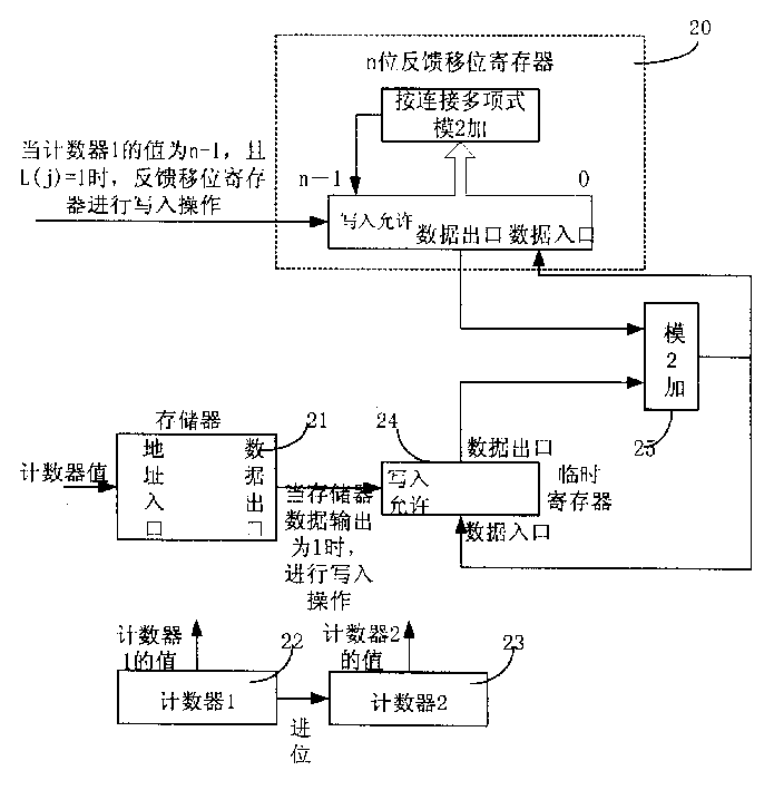
参见图2,图中示出实施本发明方法的一种装置,包括存储器21、第一计数器22、第二计数器23、临时数据寄存器24和模2加器25,用于对n位反馈移位寄存器20的初值进行计算并设置。图中的存储器21具有n×n个地址,用于保存所有的在j=0,…,n-1,k=0,…,n-1时的Sj(k)值。Referring to Fig. 2, a kind of device that implements the method of the present invention is shown among the figure, comprise
该装置的工作流程是:The workflow of the device is:
(1)将i0相位初值写入n位反馈移位寄存器20中;(1) write the i0 phase initial value in the n-bit
(2)将L表示成0至n-1的n个二进制数L(n-1)、L(n-2)、…、L(0);(2) represent L as n binary numbers L(n-1), L(n-2), ..., L(0) from 0 to n-1;
(3)将第一计数器22和第二计数器23的初值设为0,第一计数器22的值表示k,第二计数器23的值表示j;(3) the initial value of the
(4)对第二计数器23的值和第一计数器22的值进行拼接,并将第二计数器23的值作为存储器21地址的高部,将第一计数器22的值作为存储器21地址的低部,从对应地址单元(j+k)中获得Sj(k);(4) The value of the
(5)如果Sj(k)等于1,对临时数据寄存器24进行写入操作,即由模2加器25对临时数据寄存器24的输出数据和n位反馈移位寄存器20的输出数据作模2加,得到的值再写入临时数据寄存器24中;(5) If S j (k) is equal to 1, write operation is carried out to temporary data register 24, promptly modulo the output data of temporary data register 24 and the output data of n-bit
(6)如果第一计数器22的值(k)等于n-1,执行步骤(7),否则,执行步骤(10);(6) If the value (k) of the
(7)如果L(j)等于1,则把n位反馈移位寄存器20数据入口的值写入该n位反馈移位寄存器20中;(7) If L(j) is equal to 1, then write the value of n-bit
(8)如果第二计数器23的值等于n-1,执行步骤(11),否则执行步骤(9);(8) If the value of the
(9)将第二计数器23加1、第一计数器22清零,并执行步骤(4);(9) adding 1 to the
(10)第一计数器22加1,执行步骤(4);(10) The
(11)此时,m序列n位反馈移位寄存器20的值就是所需要的(i0+L)初值,即i1初值。(11) At this time, the value of the m-sequence n-bit
从上面的步骤可以看出,对m序列n位反馈移位寄存器20来说,每个j都需要作(n-1)次移位和1次初值置入,共n次操作,则n个j共需要n2次操作。这种方法需要在存储器21中对每个j所对应的Sj(k),k=0,…,n-1进行事先存储,j、k分别有n种取值,因此一共需要n2比特。As can be seen from the above steps, for the m-sequence n-bit
如果采用现有技术中简单的反馈移位方法,则需要作M次操作,0≤M≤2n-2,可以认为平均需要(2n-1-1)次操作,在n>6时,操作次数则大大超过n2。If the simple feedback shift method in the prior art is used, M operations are required, 0≤M≤2 n -2, and it can be considered that (2 n-1 -1) operations are required on average. When n>6, The number of operations greatly exceeds n 2 .
如果采用现有技术中预先存储所有相位对应的n位反馈移位寄存器初值,在需要时查表的方法,则需要具有(2n-1)×n位存储量的存储器,在n超过4的情况下大大超过了n2。If the prior art is used to store the initial values of n-bit feedback shift registers corresponding to all phases in advance, and look up the table when needed, a memory with (2 n -1)×n storage capacity is required, and when n exceeds 4 The case greatly exceeds n 2 .
而在实际应用中,n的值一般大于10,从上面的比较就可以看出本方法的巨大优势。However, in practical applications, the value of n is generally greater than 10. From the above comparison, we can see the great advantages of this method.
Claims (10)
Priority Applications (1)
| Application Number | Priority Date | Filing Date | Title |
|---|---|---|---|
| CNB011239026A CN1152503C (en) | 2001-08-02 | 2001-08-02 | Initial value carculation method for m sequence feedback shift register and its circuit |
Applications Claiming Priority (1)
| Application Number | Priority Date | Filing Date | Title |
|---|---|---|---|
| CNB011239026A CN1152503C (en) | 2001-08-02 | 2001-08-02 | Initial value carculation method for m sequence feedback shift register and its circuit |
Publications (2)
| Publication Number | Publication Date |
|---|---|
| CN1400761A CN1400761A (en) | 2003-03-05 |
| CN1152503C true CN1152503C (en) | 2004-06-02 |
Family
ID=4665349
Family Applications (1)
| Application Number | Title | Priority Date | Filing Date |
|---|---|---|---|
| CNB011239026A Expired - Fee Related CN1152503C (en) | 2001-08-02 | 2001-08-02 | Initial value carculation method for m sequence feedback shift register and its circuit |
Country Status (1)
| Country | Link |
|---|---|
| CN (1) | CN1152503C (en) |
-
2001
- 2001-08-02 CN CNB011239026A patent/CN1152503C/en not_active Expired - Fee Related
Also Published As
| Publication number | Publication date |
|---|---|
| CN1400761A (en) | 2003-03-05 |
Similar Documents
| Publication | Publication Date | Title |
|---|---|---|
| JP4851493B2 (en) | Mixed radix conversion with a priori defined statistical artifact | |
| CN1140966C (en) | Address generator and address generation method used in TURBO interleaver/deinterleaver | |
| CN1215862A (en) | Computing method and computing device | |
| CN1589429A (en) | Galois field multiplier system | |
| CN1411630A (en) | Method, apparatus and product for use in generating CRC and other remainder based codes | |
| CN1288545A (en) | Method and apparatus for arithmetic operation | |
| CN1894857A (en) | Encoding and decoding of Reed-Solomon codes using look-up tables for Galois field multiplications | |
| CN1212592A (en) | PN code generating device and mobile radio communication system | |
| CN1252566A (en) | Method and device for access control of direct memory | |
| CN1288863C (en) | Method and device for generating OVSF | |
| CN1120592C (en) | The Method of Calculating the Phase Shift Coefficient of M Sequence | |
| CN1236582C (en) | Pseudo-random sequence generator and related methods | |
| CN1714513A (en) | Address generation for the interleaver in the TURBO encoder and decoder | |
| CN1441555A (en) | Improved huffman decoding method and device | |
| CN1758591A (en) | Method, circuit and program product for processing shielded data in an encryption system | |
| CN1258710C (en) | Circuit method for high-efficiency module reduction and multiplication | |
| CN1874162A (en) | Data encoding apparatus and data encoding method | |
| CN1258148C (en) | Encryption, decryption method using high security level symmetry secret key algorithm and its encipherer | |
| CN1152503C (en) | Initial value carculation method for m sequence feedback shift register and its circuit | |
| CN100350378C (en) | Method and apparatus for parallel access to multiple memory modules | |
| CN1914847A (en) | Apparatus and method for generating random number using digital logic | |
| CN101051261A (en) | Rounding computing method and computing device therefor | |
| CN1717653A (en) | Multiplier with look up tables | |
| CN1158515A (en) | Digital filter device having bit shifter unit | |
| CN1858999A (en) | Pseudo-random sequence generating device |
Legal Events
| Date | Code | Title | Description |
|---|---|---|---|
| C10 | Entry into substantive examination | ||
| SE01 | Entry into force of request for substantive examination | ||
| C06 | Publication | ||
| PB01 | Publication | ||
| C10 | Entry into substantive examination | ||
| SE01 | Entry into force of request for substantive examination | ||
| C14 | Grant of patent or utility model | ||
| GR01 | Patent grant | ||
| CF01 | Termination of patent right due to non-payment of annual fee |
Granted publication date: 20040602 Termination date: 20150802 |
|
| EXPY | Termination of patent right or utility model |