CN114709352A - Display modules and electronic equipment - Google Patents
Display modules and electronic equipment Download PDFInfo
- Publication number
- CN114709352A CN114709352A CN202210365959.XA CN202210365959A CN114709352A CN 114709352 A CN114709352 A CN 114709352A CN 202210365959 A CN202210365959 A CN 202210365959A CN 114709352 A CN114709352 A CN 114709352A
- Authority
- CN
- China
- Prior art keywords
- display module
- area
- cover plate
- support column
- layer
- Prior art date
- Legal status (The legal status is an assumption and is not a legal conclusion. Google has not performed a legal analysis and makes no representation as to the accuracy of the status listed.)
- Granted
Links
Images




Classifications
-
- H—ELECTRICITY
- H10—SEMICONDUCTOR DEVICES; ELECTRIC SOLID-STATE DEVICES NOT OTHERWISE PROVIDED FOR
- H10K—ORGANIC ELECTRIC SOLID-STATE DEVICES
- H10K50/00—Organic light-emitting devices
- H10K50/80—Constructional details
- H10K50/84—Passivation; Containers; Encapsulations
- H10K50/841—Self-supporting sealing arrangements
-
- G—PHYSICS
- G09—EDUCATION; CRYPTOGRAPHY; DISPLAY; ADVERTISING; SEALS
- G09F—DISPLAYING; ADVERTISING; SIGNS; LABELS OR NAME-PLATES; SEALS
- G09F9/00—Indicating arrangements for variable information in which the information is built-up on a support by selection or combination of individual elements
- G09F9/30—Indicating arrangements for variable information in which the information is built-up on a support by selection or combination of individual elements in which the desired character or characters are formed by combining individual elements
-
- H—ELECTRICITY
- H10—SEMICONDUCTOR DEVICES; ELECTRIC SOLID-STATE DEVICES NOT OTHERWISE PROVIDED FOR
- H10K—ORGANIC ELECTRIC SOLID-STATE DEVICES
- H10K50/00—Organic light-emitting devices
- H10K50/80—Constructional details
- H10K50/84—Passivation; Containers; Encapsulations
- H10K50/842—Containers
- H10K50/8426—Peripheral sealing arrangements, e.g. adhesives, sealants
-
- H—ELECTRICITY
- H10—SEMICONDUCTOR DEVICES; ELECTRIC SOLID-STATE DEVICES NOT OTHERWISE PROVIDED FOR
- H10K—ORGANIC ELECTRIC SOLID-STATE DEVICES
- H10K50/00—Organic light-emitting devices
- H10K50/80—Constructional details
- H10K50/84—Passivation; Containers; Encapsulations
- H10K50/842—Containers
- H10K50/8428—Vertical spacers, e.g. arranged between the sealing arrangement and the OLED
-
- H—ELECTRICITY
- H10—SEMICONDUCTOR DEVICES; ELECTRIC SOLID-STATE DEVICES NOT OTHERWISE PROVIDED FOR
- H10K—ORGANIC ELECTRIC SOLID-STATE DEVICES
- H10K59/00—Integrated devices, or assemblies of multiple devices, comprising at least one organic light-emitting element covered by group H10K50/00
- H10K59/10—OLED displays
Landscapes
- Physics & Mathematics (AREA)
- Optics & Photonics (AREA)
- General Physics & Mathematics (AREA)
- Engineering & Computer Science (AREA)
- Theoretical Computer Science (AREA)
- Electroluminescent Light Sources (AREA)
Abstract
本申请实施例提供的显示模组及电子设备,涉及显示技术领域。在显示模组中,支撑柱分布区域的外周沿封装层在封装盖板上的延伸方向延伸,支撑柱分布区域的外周在显示模组的边角区域处与封装层之间的距离,不大于支撑柱分布区域的外周在显示模组的长边和宽边位置处与封装层之间的距离。如此设计可以在将封装盖板与显示基板进行封装后,通过显示基板中设置的支撑柱对封装盖板进行有效支撑,特别是对显示模组的边角区域处对应的封装盖板进行有效支撑,以此减小在显示基板和封装盖板之间形成不同微腔的尺寸差异,从而达到弱化牛顿环现象提升显示效果的目的。

The display module and the electronic device provided by the embodiments of the present application relate to the field of display technology. In the display module, the outer periphery of the support column distribution area extends along the extending direction of the packaging layer on the packaging cover plate, and the distance between the outer periphery of the support column distribution area and the packaging layer at the corner area of the display module is not greater than The distance between the outer periphery of the distribution area of the support column and the encapsulation layer at the position of the long side and the broad side of the display module. Such a design can effectively support the package cover plate through the support columns provided in the display substrate after the package cover plate and the display substrate are encapsulated, especially the corresponding package cover plate at the corner area of the display module can be effectively supported. , so as to reduce the size difference of different microcavities formed between the display substrate and the package cover plate, so as to achieve the purpose of weakening the Newton's ring phenomenon and improving the display effect.
Description
技术领域technical field
本申请涉及显示技术领域,具体而言,涉及一种显示模组及电子设备。The present application relates to the field of display technology, and in particular, to a display module and an electronic device.
背景技术Background technique
电子设备(比如,智能终端设备)在使用时会存在比较明显的牛顿环现象,特别是在环境光线较强的户外,此现象更为明显,进而影响显示效果,给用户造成不好的使用体验。为此弱化牛顿环现象对显示效果的影响成为本领域技术人员急需要解决的技术问题。Electronic equipment (such as smart terminal equipment) will have obvious Newton's ring phenomenon when in use, especially in the outdoors with strong ambient light, this phenomenon is more obvious, which will affect the display effect and cause a bad user experience. . Therefore, weakening the influence of the Newton ring phenomenon on the display effect has become a technical problem that those skilled in the art urgently need to solve.
发明内容SUMMARY OF THE INVENTION
为了克服上述技术背景中所提及的技术问题,本申请实施例提供一种显示模组及电子设备。In order to overcome the technical problems mentioned in the above technical background, embodiments of the present application provide a display module and an electronic device.
本申请的第一方面,提供一种显示模组,所述显示模组包括显示基板、封装盖板以及封装层;A first aspect of the present application provides a display module, the display module includes a display substrate, an encapsulation cover plate and an encapsulation layer;
所述封装层靠近所述显示基板和所述封装盖板的边缘且位于所述显示基板和所述封装盖板之间;the encapsulation layer is close to the edge of the display substrate and the encapsulation cover plate and is located between the display substrate and the encapsulation cover plate;
所述显示基板包括基板层以及设置在所述基板层上的支撑柱,所述支撑柱分布在所述封装层围合形成的区域内;The display substrate includes a substrate layer and support pillars disposed on the substrate layer, the support pillars are distributed in an area enclosed and formed by the encapsulation layer;
所述支撑柱分布区域的外周沿所述封装层在所述封装盖板上的延伸方向延伸;所述支撑柱分布区域的外周在所述显示模组的边角区域处与所述封装层之间的距离,不大于所述支撑柱分布区域的外周在所述显示模组的长边和宽边位置处与所述封装层之间的距离。The outer circumference of the support column distribution area extends along the extension direction of the packaging layer on the packaging cover plate; the outer circumference of the support column distribution area is located between the corner area of the display module and the packaging layer. The distance between them is not greater than the distance between the outer periphery of the support column distribution area and the encapsulation layer at the positions of the long side and the broad side of the display module.
在本申请的一种可能实施例中,所述支撑柱分布区域的外周与所述封装层在所述封装盖板上的延伸方向平行。In a possible embodiment of the present application, the outer periphery of the support pillar distribution area is parallel to the extending direction of the packaging layer on the packaging cover plate.
在本申请的一种可能实施例中,所述支撑柱分布区域的外周在所述显示模组的边角区域朝向所述封装层方向凸起。In a possible embodiment of the present application, the outer periphery of the support column distribution area is convex toward the encapsulation layer in the corner area of the display module.
在本申请的一种可能实施例中,所述支撑柱分布区域的外周在所述显示模组的长边或宽边的区域处包括朝向所述封装层方向的凸起区域;In a possible embodiment of the present application, the outer periphery of the support column distribution area includes a convex area facing the direction of the encapsulation layer at the area of the long side or the broad side of the display module;
优选地,所述凸起区域位于所述显示模组的长边或宽边的四分之一或二分之一的区域处。Preferably, the raised area is located at a quarter or half of the long side or wide side of the display module.
在本申请的一种可能实施例中,在所述显示模组的边角区域处,所述支撑柱分布区域的外周与所述封装层之间的距离为0.9mm~1.7mm;In a possible embodiment of the present application, at the corner area of the display module, the distance between the outer periphery of the support column distribution area and the encapsulation layer is 0.9 mm to 1.7 mm;
所述支撑柱分布区域的外周与所述封装层之间的距离为0.9mm~1.3mm。The distance between the outer periphery of the support pillar distribution area and the encapsulation layer is 0.9 mm˜1.3 mm.
在本申请的一种可能实施例中,在垂直于显示模组出光面的方向,所述支撑柱被压缩,所述支撑柱的压缩高度为所述支撑柱相对于所述封装层高出的高度。In a possible embodiment of the present application, in a direction perpendicular to the light-emitting surface of the display module, the support column is compressed, and the compressed height of the support column is the height of the support column higher than the encapsulation layer. high.
在本申请的一种可能实施例中,所述封装层的材料包括玻璃粉、填充料以及粘合剂,其中,所述玻璃粉的质量百分比为20%~80%,所述填充料的质量百分比为5%~40%,所述粘合剂的质量百分比为10%~40%;In a possible embodiment of the present application, the material of the encapsulation layer includes glass frit, a filler and a binder, wherein the mass percentage of the glass frit is 20% to 80%, and the mass of the filler The percentage is 5% to 40%, and the mass percentage of the adhesive is 10% to 40%;
所述支撑柱的材料为聚酰亚胺。The material of the support column is polyimide.
在本申请的一种可能实施例中,所述支撑柱的压缩高度为0um~1.59um;In a possible embodiment of the present application, the compression height of the support column is 0um~1.59um;
优选地,所述支撑柱的压缩高度为0.44um~0.6um。Preferably, the compression height of the support column is 0.44um~0.6um.
在本申请的一种可能实施例中,所述支撑柱的高度由所述支撑柱分布区域的中心向所述支撑柱分布区域的外周增大。In a possible embodiment of the present application, the height of the support column increases from the center of the support column distribution area to the outer circumference of the support column distribution area.
本申请的第二方面,提供一种电子设备,所述电子设备包括第一方面中任意一种可能实施例中的显示模组。In a second aspect of the present application, an electronic device is provided, and the electronic device includes the display module in any of the possible embodiments of the first aspect.
本申请实施例提供一种显示模组及电子设备,在显示模组中,支撑柱分布区域的外周沿封装层在封装盖板上的延伸方向延伸,支撑柱分布区域的外周在显示模组的边角区域处与封装层之间的距离,不大于支撑柱分布区域的外周在显示模组的长边和宽边位置处与封装层之间的距离。如此设计可以在将封装盖板与显示基板进行封装后,通过显示基板中设置的支撑柱对封装盖板进行有效支撑,特别是对显示模组的边角区域处对应的封装盖板进行有效支撑,降低封装盖板在边角区域处的形变,如此可以降低整个封装盖板形变曲率,进而减小在显示基板和封装盖板之间形成不同微腔的尺寸差异,使得经过不同微腔反射的光的光程间差异减小,达到弱化牛顿环现象保证显示效果的目的。Embodiments of the present application provide a display module and an electronic device. In the display module, the outer circumference of the support column distribution area extends along the extending direction of the packaging layer on the packaging cover plate, and the outer circumference of the support column distribution area is located on the surface of the display module. The distance between the corner area and the encapsulation layer is not greater than the distance between the outer periphery of the support column distribution area and the encapsulation layer at the positions of the long and broad sides of the display module. Such a design can effectively support the package cover plate through the support columns provided in the display substrate after the package cover plate and the display substrate are encapsulated, especially the corresponding package cover plate at the corner area of the display module can be effectively supported. , reduce the deformation of the package cover at the corner area, so that the deformation and curvature of the entire package cover can be reduced, thereby reducing the size difference of different microcavities formed between the display substrate and the package cover. The difference between the optical paths of the light is reduced, and the purpose of weakening the Newton's ring phenomenon and ensuring the display effect is achieved.
附图说明Description of drawings
为了更清楚地说明本申请实施例的技术方案,下面将对实施例中所需要使用的附图作简单地介绍,应当理解,以下附图仅示出了本申请的某些实施例,因此不应被看作是对范围的限定,对于本领域普通技术人员来讲,在不付出创造性劳动的前提下,还可以根据这些附图获得其他相关的附图。In order to illustrate the technical solutions of the embodiments of the present application more clearly, the following drawings will briefly introduce the drawings that need to be used in the embodiments. It should be understood that the following drawings only show some embodiments of the present application, and therefore do not It should be regarded as a limitation of the scope, and for those of ordinary skill in the art, other related drawings can also be obtained according to these drawings without any creative effort.
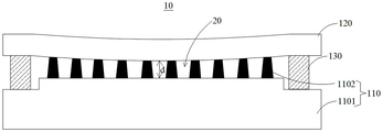
图1示例了现有显示模组在封装前的部分膜层结构示意图;FIG. 1 illustrates a schematic diagram of a partial film layer structure of an existing display module before encapsulation;
图2示例了现有显示模组在封装后的部分膜层结构示意图;FIG. 2 illustrates a schematic diagram of a partial film layer structure of an existing display module after encapsulation;
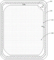
图3示例了支撑柱分布区域与封装层之间的位置关系示意图;FIG. 3 illustrates a schematic diagram of the positional relationship between the support pillar distribution area and the encapsulation layer;
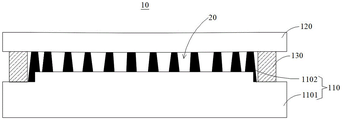
图4示例了本申请实施例提供的显示模组在封装后的膜层结构示意图;FIG. 4 illustrates a schematic diagram of the film layer structure of the display module provided by the embodiment of the present application after packaging;
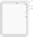
图5示例了本申请实施例提供的支撑柱分布区域与封装层之间的位置关系示意图之一;FIG. 5 illustrates one of the schematic diagrams of the positional relationship between the support column distribution area and the encapsulation layer provided by the embodiment of the present application;
图6示例了本申请实施例提供的支撑柱分布区域与封装层之间的位置关系示意图之二;FIG. 6 illustrates the second schematic diagram of the positional relationship between the support column distribution area and the encapsulation layer provided by the embodiment of the present application;
图7示例了本申请实施例提供的支撑柱分布区域与封装层之间的位置关系示意图之三;FIG. 7 illustrates the third schematic diagram of the positional relationship between the support column distribution area and the encapsulation layer provided by the embodiment of the present application;
图8示例了本申请实施例提供的显示模组在封装前的部分膜层结构示意图;FIG. 8 illustrates a schematic diagram of a partial film layer structure of the display module provided by the embodiment of the present application before encapsulation;
图9示例了本申请实施例提供的不同支撑柱与封装层的高度差与封装盖板形变量之间的关系图;FIG. 9 illustrates a relationship diagram between the height difference between different support columns and the packaging layer and the deformation amount of the packaging cover provided by the embodiment of the present application;
图10示例了本申请实施例提供的一种支撑柱的分布示意图。FIG. 10 illustrates a schematic diagram of the distribution of a support column provided by an embodiment of the present application.
图标:10-显示模组;110-显示基板;101-边角区域;1101-基板层;1102-支撑柱;120-封装盖板;130-封装层;300-支撑柱分布区域;310-支撑柱分布区域的外周;3101-凸起区域;20-微腔。Icon: 10-display module; 110-display substrate; 101-corner area; 1101-substrate layer; 1102-support column; 120-package cover plate; 130-package layer; 300-support column distribution area; 310-support perimeter of the column distribution area; 3101 - raised area; 20 - microcavity.
具体实施方式Detailed ways
为使本申请实施例的目的、技术方案和优点更加清楚,下面将结合本申请实施例中的附图,对本申请实施例中的技术方案进行清楚、完整地描述,显然,所描述的实施例是本申请一部分实施例,而不是全部的实施例。通常在此处附图中描述和示出的本申请实施例的组件可以以各种不同的配置来布置和设计。In order to make the purposes, technical solutions and advantages of the embodiments of the present application clearer, the technical solutions in the embodiments of the present application will be described clearly and completely below with reference to the drawings in the embodiments of the present application. Obviously, the described embodiments It is a part of the embodiments of the present application, but not all of the embodiments. The components of the embodiments of the present application generally described and illustrated in the drawings herein may be arranged and designed in a variety of different configurations.
因此,以下对在附图中提供的本申请的实施例的详细描述并非旨在限制要求保护的本申请的范围,而是仅仅表示本申请的选定实施例。基于本申请中的实施例,本领域普通技术人员在没有作出创造性劳动前提下所获得的所有其他实施例,都属于本申请保护的范围。Thus, the following detailed description of the embodiments of the application provided in the accompanying drawings is not intended to limit the scope of the application as claimed, but is merely representative of selected embodiments of the application. Based on the embodiments in the present application, all other embodiments obtained by those of ordinary skill in the art without creative work fall within the protection scope of the present application.
应注意到:相似的标号和字母在下面的附图中表示类似项,因此,一旦某一项在一个附图中被定义,则在随后的附图中不需要对其进行进一步定义和解释。It should be noted that like numerals and letters refer to like items in the following figures, so once an item is defined in one figure, it does not require further definition and explanation in subsequent figures.
在本申请的描述中,需要说明的是,术语“上”、“下”等指示的方位或位置关系为基于附图所示的方位或位置关系,或者是该申请产品使用时惯常摆放的方位或位置关系,仅是为了便于描述本申请和简化描述,而不是指示或暗示所指的装置或元件必须具有特定的方位、以特定的方位构造和操作,因此不能理解为对本申请的限制。此外,术语“第一”、“第二”等仅用于区分描述,而不能理解为指示或暗示相对重要性。In the description of this application, it should be noted that the orientation or positional relationship indicated by the terms "upper", "lower", etc. is based on the orientation or positional relationship shown in the accompanying drawings, or is usually placed when the product of the application is used. The orientation or positional relationship is only for the convenience of describing the present application and simplifying the description, rather than indicating or implying that the referred device or element must have a specific orientation, be constructed and operated in a specific orientation, and therefore should not be construed as a limitation on the present application. Furthermore, the terms "first", "second", etc. are only used to differentiate the description and should not be construed to indicate or imply relative importance.
需要说明的是,在不冲突的情况下,本申请的实施例中的不同特征之间可以相互结合。It should be noted that, in the case of no conflict, different features in the embodiments of the present application may be combined with each other.
为了便于说明导致前述背景技术中所提及的技术问题的具体原因,下面先对显示模组的膜层结构进行介绍,请参照图1及图2,图1示例了显示模组10在封装前的部分膜层结构示意图,图2示例了显示模组10在封装后的部分膜层结构示意图。其中,显示模组10可以包括显示基板110、封装盖板120及封装层130,封装层130位于封装盖板120的一侧且靠近封装盖板120的边缘沿封装盖板120的边缘延伸。显示基板110可以包括基板层1101和设置在基板层1101的支撑柱1102,支撑柱1102可以设置在相邻发光像素之间,支撑柱1102可以用于支撑封装盖板120以防止封装盖板120压伤发光像素。在通过封装层130完成显示基板110和封装盖板120的密封封装之后,在显示基板110和封装盖板120之间的内部空间形成类真空环境(大气压强很小),在外界大气压和封装盖板120自身重力的作用下,封装盖板120可能会发生微观形变形成一类似浴盆的具有一定曲率的凹陷面,如此会在显示基板110和封装盖板120之间的内部空间形成许多的微腔20,在垂直于显示模组10的出光面方向,不同位置处的微腔20的尺寸d存在较大差异,在环境光入射到显示模组10上时,在不同微腔20上下面反射光的光程存在差异,在反射后会相互干涉,从而在显示模组10中出现牛顿环现象,影响显示效果。其中,凹陷面的曲率越大对应的封装盖板120的形变越大,不同微腔20之间的尺寸d的差异越大,牛顿环现象越明显。In order to explain the specific reasons for the technical problems mentioned in the aforementioned background art, the film layer structure of the display module will be introduced first. Please refer to FIG. 1 and FIG. 2. FIG. 1 illustrates the
发明人进一步研究发现,请再次参照图2,封装盖板120在其边缘区域处的形变量较大,且边角区域101相对其他边缘区域更容易发生形变。发明人通过拆解显示模组10发现,请参照图3,在边角区域101,支撑柱分布区域的外周310距封装层130之间的距离H1相比于其他区域中支撑柱分布区域的外周310距封装层的距离(支撑柱分布区域的外周310在显示模组10的宽边位置处与封装层130之间的距离H2,或支撑柱分布区域的外周310在显示模组10的长边位置处与封装层130之间的距离H3)大,导致在边角区域101的封装盖板120得不到有效支撑,使得封装盖板120的形变由封装盖板120的边缘朝向封装盖板120的中心区域延伸,从而导致整个封装盖板120会产生较大的形变,进而使得不同微腔20之间的尺寸d的差异较大,这会使牛顿环现象更加严重。The inventor has further researched and found that, referring to FIG. 2 again, the
为了解决上述技术问题。发明人创新性的设计以下技术方案,下面将结合附图对本申请的具体实现方案进行详细说明。In order to solve the above technical problems. The inventor has innovatively designed the following technical solutions, and the specific implementation solutions of the present application will be described in detail below with reference to the accompanying drawings.
所应说明的是,以上现有技术中的方案所存在的缺陷,均是发明人在经过实践并仔细研究后得出的结果,因此,上述技术问题的发现过程以及下文中本申请实施例针对上述问题所提出的解决方案,都应该是发明人在发明创造过程中对本申请做出的贡献,而不应当理解为本领域技术人员所公知的技术内容。It should be noted that the defects existing in the above solutions in the prior art are the results obtained by the inventor after practice and careful research. Therefore, the discovery process of the above-mentioned technical problems and the following examples of the present application are aimed at. The solutions proposed for the above problems should all be contributions made by the inventor to the present application in the process of invention and creation, and should not be understood as technical contents known to those skilled in the art.
为了更好的描述本申请实施例提供的技术方案,请参照图4及图5,图4示出了本申请实施例提供的显示模组的膜层结构示意图;图5示出了本申请实施例提供的支撑柱分布区域300与封装层130之间的位置关系示意图之一。详细地,本实施例中,显示模组10可以包括显示基板110、封装盖板120及封装层130,封装层130靠近显示基板110和封装盖板120的边缘且位于显示基板110与封装盖板120之间。显示基板110可以包括基板层1101和设置在基板层1101上的支撑柱1102,支撑柱1102分布在封装层130围合形成的区域内。In order to better describe the technical solutions provided by the embodiments of the present application, please refer to FIG. 4 and FIG. 5 . FIG. 4 shows a schematic diagram of the film layer structure of the display module provided by the embodiments of the present application; FIG. 5 shows the implementation of the present application. One of the schematic diagrams of the positional relationship between the support
在本实施例中,支撑柱1102在封装层130围合形成的区域内分布成一支撑柱分布区域300。支撑柱分布区域的外周310沿封装层130在封装盖板120上的延伸方向延伸,支撑柱分布区域的外周310在显示模组的边角区域101处与封装层130之间的距离H1,不大于支撑柱分布区域的外周310在显示模组10的宽边位置处与封装层130之间的距离H2和支撑柱分布区域的外周310在显示模组10的长边位置处与封装层130之间的距离H3,其中,与封装层130之间的距离是可以是与封装层130朝向支撑柱分布区域300一侧的距离,距离H2和距离H3可以相同也可以不同。显示模组10的长边和宽边相邻,显示模组10的长边对应显示模组10的边缘中较长的一侧边缘,显示模组10的宽边对应显示模组10的边缘中较短的一侧边缘,在显示模组10的相邻两边缘的长度相同时,可以将其中一侧边缘作为显示模组10的长边,另一侧边缘作为显示模组10的宽边,边角区域101由显示模组10的长边和显示模组10的宽边相交形成,示例性地,边角区域101可以为弧形区域。In this embodiment, the
在上述结构中,可以在将封装盖板120与显示基板110进行封装后,通过显示基板110中设置的支撑柱1102对封装盖板120进行有效支撑,特别是对显示模组10的边角区域101处对应的封装盖板120进行有效支撑,进而减小封装盖板120在边角区域101的形变量,降低封装盖板120在边角区域101处的形变,如此可以降低整个封装盖板120形变曲率,以此减小在显示基板110和封装盖板120之间形成不同微腔20的尺寸差异,从而达到弱化牛顿环现象保证显示效果的目的。In the above structure, after the
在本申请实施例的一种可能的实施方式中,支撑柱分布区域的外周310与封装层130在封装盖板120上的延伸方向平行,即在任意一个位置,支撑柱分布区域的外周310与封装层130之间的距离相等(距离H1=距离H2=距离H3)。如此设计,可以在封装盖板120与显示基板110封装后,使得封装盖板120靠近封装层130的区域均能被有效支撑,以此降低封装盖板120的形变量。In a possible implementation of the embodiment of the present application, the
请参照图6,图6示例了本申请实施例提供的支撑柱分布区域300与封装层130之间的位置关系示意图之二。在本申请实施例的另一种可能的实施方式中,支撑柱分布区域的外周310在显示模组10的边角区域101朝向封装层130的方向凸起,所形成的凸起可以使得支撑柱分布区域的外周310在显示模组10的边角区域101处与封装层130之间的距离H1,小于支撑柱分布区域的外周310在显示模组10的宽边位置处与封装层130之间的距离H2和支撑柱分布区域的外周310在显示模组10的长边位置处与封装层130之间的距离H3,如此可以增加边角区域101处封装盖板120的支撑面积,使得边角区域101处的封装盖板120的形变量能被很好的控制,从而能减小封装盖板120整体的形变量。Please refer to FIG. 6 . FIG. 6 illustrates the second schematic diagram of the positional relationship between the support
发明人进一步研究发现,在封装时,一般采用激光烧结封装材料层的方式进行,通过控制激光沿着封装材料层的延伸方向均匀运动,烧结过程中会存在封装材料受热不均的问题,比如,开始位置点受热2秒,靠近该位置的封装材料会受开始位置点的激光影响对其进行烧结的开始温度就会比开始位置点高,激光作用时间相同的情况下,最终形成的封装层130的高度会存在差异。另外,在封装盖板120上制作封装层130时,因封装材料涂敷不均也会导致最终形成的封装层130的高度会存在差异。为了解决上述问题,请参照图7,图7示例了本申请实施例提供的支撑柱分布区域300与封装层130之间的位置关系示意图之三。进一步地,在本申请实施例中,支撑柱分布区的外周310在显示模组10的长边或宽边的区域处包括朝向封装层130的凸起区域3101。凸起区域3101中的支撑柱1102可以对边缘位置处的封装盖板120进行有效支撑以抵消封装层130的高度差异带来的封装盖板120的压力差异,确保整个封装盖板120在封装后的整体形变量不会过大。优选地,凸起区域3101可以位于显示模组10的长边或宽边的四分之一和/或二分之一区域处,其中,四分之一区域和二分之一区域是指区域的中心分别位于四分之一和二分之一位置处的区域。The inventor further researched and found that during packaging, the packaging material layer is generally laser sintered. By controlling the laser to move uniformly along the extension direction of the packaging material layer, there will be a problem of uneven heating of the packaging material during the sintering process. For example, The starting point is heated for 2 seconds, and the encapsulation material close to this position will be affected by the laser at the starting point and the starting temperature of sintering will be higher than that at the starting point. When the laser action time is the same, the
发明人通过大量的实验发现,在显示模组10的边角区域101处,支撑柱分布区域的外周310与封装层130之间的距离为0.9mm~1.7mm时,封装盖板120在边角区域101的形变量较小,整个封装盖板120形变弯曲的曲率也较小。优选地,支撑柱分布区域的外周310与封装层130之间的距离为0.9mm~1.3mm。The inventor found through a large number of experiments that, at the
进一步地,在本申请实施例中,在垂直于显示模组10出光面的方向,支撑柱1102被压缩,请参照图8,在封装时将显示基板110与封装盖板120对位,支撑柱1102的被压缩高度为封装层130与显示基板110之间的距离H4和支撑柱1102与封装盖板120之间的距离H5之间的差,其中,距离H4与距离H5之间的差定义为封装前支撑柱1102高出封装层130的高度。Further, in the embodiment of the present application, in the direction perpendicular to the light-emitting surface of the
在本申请实施例中,封装层130的材料可以包括玻璃粉、填充料以及粘合剂,其中,玻璃粉的质量百分比为20%~80%,填充料的质量百分比为5%~40%,粘合剂的质量百分比为10%~40%,支撑柱的材料为聚酰亚胺。玻璃粉可以包括V2O5、P2O5、Fe2O3、TeO2、BaO、SiO2、B2O3、PbO及SnO,填充料可以包括陶瓷粉或难熔氧化物,粘合剂可以包括二甘醇一丁醚。In the embodiment of the present application, the material of the
请参照图9,图9示例了不同支撑柱1102和封装层130的高度差与封装盖板120的形变量之间的关系图,其中高度差为负表示支撑柱1102的高度低于封装层130的高度,高度差为正表示支撑柱1102的高度高于封装层130的高度;封装盖板形变量是指封装盖板120的最大形变量,数值越大表示形变越严重;path-封装盖板变形量表示封装盖板120中最大两处形变位置连线路径上的形变量,path-封装盖板变形量越大表示形变越严重,两处形变位置之间的变形曲率越大,在本实施例中,采用path-封装盖板变形量对封装盖板120的变形进行量化。如图9所示,高度差在0~1.59um时,path-封装盖板变形量维持在25nm以内,而其他高度差对应的path-封装盖板变形量较大。具体地,高度差为0.44um时,封装盖板120的path-封装盖板变形量为3.1nm,高度差为0.44um~0.6um时,path-封装盖板变形量较小(比如,在18nm以内)。Please refer to FIG. 9 . FIG. 9 illustrates the relationship between the height difference of
发明人还发现,封装盖板120在靠近封装层130的区域所受的形变压力大于远离封装层130的区域所受的形变压力,请参照图10,图10示例了一种支撑柱1102的分布示意图,在本申请实施例中,支撑柱1102的高度由支撑柱分布区域300的中心向支撑柱分布区域的外周310(图中箭头方向)增大,以使得在形变压力较大的区域布置高度更高的支撑柱1102,根据形变压力的不同布局不同高度的支撑柱1102,可以使得封装盖板120能被有效支撑,降低整个封装盖板120的形变量,从而弱化牛顿环效应,提高显示效果。The inventor also found that the deformation pressure of the
本申请实施例还提供一种电子设备,该电子设备可以包括前面实施例描述的显示模组10,采用该显示模组10的电子设备具有良好的显示性能,可以提高用户的使用体验。Embodiments of the present application further provide an electronic device, which may include the
本申请实施例提供的显示模组及电子设备,在显示模组中,支撑柱分布区域的外周沿封装层在封装盖板上的延伸方向延伸,支撑柱分布区域的外周在显示模组的边角区域处与封装层之间的距离,不大于支撑柱分布区域的外周在显示模组的长边和宽边位置处与封装层之间的距离。如此设计可以在将封装盖板与显示基板进行封装后,通过显示基板中设置的支撑柱对封装盖板进行有效支撑,特别是对显示模组的边角区域处对应的封装盖板进行有效支撑,降低封装盖板在边角区域处的形变,如此可以降低整个封装盖板形变曲率,进而减小在显示基板和封装盖板之间形成不同微腔的尺寸差异,使得经过不同微腔反射的光的光程差差异减小,达到弱化牛顿环现象提升显示效果的目的。In the display module and the electronic device provided by the embodiments of the present application, in the display module, the outer circumference of the support column distribution area extends along the extending direction of the packaging layer on the packaging cover plate, and the outer circumference of the support column distribution area is on the side of the display module. The distance between the corner area and the encapsulation layer is not greater than the distance between the outer periphery of the support column distribution area and the encapsulation layer at the positions of the long and broad sides of the display module. Such a design can effectively support the package cover plate through the support columns provided in the display substrate after the package cover plate and the display substrate are encapsulated, especially the corresponding package cover plate at the corner area of the display module can be effectively supported. , reduce the deformation of the package cover at the corner area, so that the deformation and curvature of the entire package cover can be reduced, thereby reducing the size difference of different microcavities formed between the display substrate and the package cover. The difference of the optical path difference of the light is reduced, so as to achieve the purpose of weakening the Newton's ring phenomenon and improving the display effect.
以上所述仅为本申请的优选实施例而已,并不用于限制本申请,对于本领域的技术人员来说,本申请可以有各种更改和变化。凡在本申请的精神和原则之内,所作的任何修改、等同替换、改进等,均应包含在本申请的保护范围之内。The above descriptions are only preferred embodiments of the present application, and are not intended to limit the present application. For those skilled in the art, the present application may have various modifications and changes. Any modification, equivalent replacement, improvement, etc. made within the spirit and principle of this application shall be included within the protection scope of this application.
Claims (10)
Priority Applications (1)
| Application Number | Priority Date | Filing Date | Title |
|---|---|---|---|
| CN202210365959.XA CN114709352B (en) | 2022-04-08 | 2022-04-08 | Display module and electronic equipment |
Applications Claiming Priority (1)
| Application Number | Priority Date | Filing Date | Title |
|---|---|---|---|
| CN202210365959.XA CN114709352B (en) | 2022-04-08 | 2022-04-08 | Display module and electronic equipment |
Publications (2)
| Publication Number | Publication Date |
|---|---|
| CN114709352A true CN114709352A (en) | 2022-07-05 |
| CN114709352B CN114709352B (en) | 2025-07-22 |
Family
ID=82171846
Family Applications (1)
| Application Number | Title | Priority Date | Filing Date |
|---|---|---|---|
| CN202210365959.XA Active CN114709352B (en) | 2022-04-08 | 2022-04-08 | Display module and electronic equipment |
Country Status (1)
| Country | Link |
|---|---|
| CN (1) | CN114709352B (en) |
Citations (4)
| Publication number | Priority date | Publication date | Assignee | Title |
|---|---|---|---|---|
| CN106526964A (en) * | 2016-11-30 | 2017-03-22 | 厦门天马微电子有限公司 | Display panel |
| CN208045551U (en) * | 2018-01-19 | 2018-11-02 | 昆山国显光电有限公司 | Encapsulating structure and Organnic electroluminescent device |
| CN110048020A (en) * | 2019-04-12 | 2019-07-23 | 昆山国显光电有限公司 | Display panel and preparation method thereof, display device |
| CN113516925A (en) * | 2021-06-29 | 2021-10-19 | 昆山国显光电有限公司 | Display panel, manufacturing method thereof and display device |
-
2022
- 2022-04-08 CN CN202210365959.XA patent/CN114709352B/en active Active
Patent Citations (4)
| Publication number | Priority date | Publication date | Assignee | Title |
|---|---|---|---|---|
| CN106526964A (en) * | 2016-11-30 | 2017-03-22 | 厦门天马微电子有限公司 | Display panel |
| CN208045551U (en) * | 2018-01-19 | 2018-11-02 | 昆山国显光电有限公司 | Encapsulating structure and Organnic electroluminescent device |
| CN110048020A (en) * | 2019-04-12 | 2019-07-23 | 昆山国显光电有限公司 | Display panel and preparation method thereof, display device |
| CN113516925A (en) * | 2021-06-29 | 2021-10-19 | 昆山国显光电有限公司 | Display panel, manufacturing method thereof and display device |
Also Published As
| Publication number | Publication date |
|---|---|
| CN114709352B (en) | 2025-07-22 |
Similar Documents
| Publication | Publication Date | Title |
|---|---|---|
| JP6284659B2 (en) | Light emitting diode package structure | |
| CN109860422B (en) | Display panels and display devices | |
| CN107591374B (en) | Sensor Package Structure | |
| US11793018B2 (en) | OLED packaging structure and packaging method, and display apparatus | |
| CN115623813B (en) | Display panel, display device and packaging method | |
| JP2019036701A (en) | Sensor package structure | |
| US20210343970A1 (en) | Display panel and manufacturing method therefor, and display device | |
| CN109545826A (en) | Display panel, manufacturing method thereof and display device comprising display panel | |
| CN111968521A (en) | Display panel and display device | |
| CN107393907A (en) | Display panel and display device | |
| CN105185810A (en) | Display substrate and manufacturing method, display panel and display apparatus | |
| CN108232043A (en) | Display panel and its manufacturing method, display device | |
| CN108281472B (en) | A display component, display device and manufacturing method | |
| CN113570966A (en) | Display device and spliced screen | |
| CN111740026A (en) | Flexible display panel | |
| CN113589590A (en) | Backlight module and display device | |
| CN109546003B (en) | Display panels and display devices | |
| CN105070743B (en) | Array base palte and preparation method thereof, display panel, display device | |
| CN113097418B (en) | Display panel, manufacturing method of display panel and display device | |
| CN118131545B (en) | Display panel and display device | |
| WO2025129952A1 (en) | Display panel and display device | |
| CN117935680A (en) | Display module, method for manufacturing display module, and display device | |
| CN114709352A (en) | Display modules and electronic equipment | |
| CN109493736B (en) | Display panel and display device thereof | |
| CN114530567B (en) | Display panel, display device, and packaging method of display panel |
Legal Events
| Date | Code | Title | Description |
|---|---|---|---|
| PB01 | Publication | ||
| PB01 | Publication | ||
| SE01 | Entry into force of request for substantive examination | ||
| SE01 | Entry into force of request for substantive examination | ||
| GR01 | Patent grant | ||
| GR01 | Patent grant |