CN114679158B - Periodic signal generating device, signal processing system and periodic signal generating method thereof - Google Patents
Periodic signal generating device, signal processing system and periodic signal generating method thereof Download PDFInfo
- Publication number
- CN114679158B CN114679158B CN202210595557.9A CN202210595557A CN114679158B CN 114679158 B CN114679158 B CN 114679158B CN 202210595557 A CN202210595557 A CN 202210595557A CN 114679158 B CN114679158 B CN 114679158B
- Authority
- CN
- China
- Prior art keywords
- input
- signal
- output
- module
- dual
- Prior art date
- Legal status (The legal status is an assumption and is not a legal conclusion. Google has not performed a legal analysis and makes no representation as to the accuracy of the status listed.)
- Active
Links
Images


Classifications
-
- H—ELECTRICITY
- H03—ELECTRONIC CIRCUITRY
- H03K—PULSE TECHNIQUE
- H03K3/00—Circuits for generating electric pulses; Monostable, bistable or multistable circuits
- H03K3/02—Generators characterised by the type of circuit or by the means used for producing pulses
- H03K3/027—Generators characterised by the type of circuit or by the means used for producing pulses by the use of logic circuits, with internal or external positive feedback
- H03K3/03—Astable circuits
- H03K3/0315—Ring oscillators
-
- G—PHYSICS
- G01—MEASURING; TESTING
- G01R—MEASURING ELECTRIC VARIABLES; MEASURING MAGNETIC VARIABLES
- G01R1/00—Details of instruments or arrangements of the types included in groups G01R5/00 - G01R13/00 and G01R31/00
- G01R1/28—Provision in measuring instruments for reference values, e.g. standard voltage, standard waveform
-
- G—PHYSICS
- G01—MEASURING; TESTING
- G01R—MEASURING ELECTRIC VARIABLES; MEASURING MAGNETIC VARIABLES
- G01R35/00—Testing or calibrating of apparatus covered by the other groups of this subclass
- G01R35/005—Calibrating; Standards or reference devices, e.g. voltage or resistance standards, "golden" references
Abstract
The invention discloses a periodic signal generating device, a signal processing system and a periodic signal generating method thereof, wherein the device comprises: a control logic unit for sending a reset signal; the input detection unit receives a corresponding input signal after resetting and detects the arrival time of the rising edge of the input signal; the dual-input dual-output annular oscillation unit is used for copying the rising edge information of the corresponding input signal to obtain a corresponding reset signal; the state detection unit is used for detecting the phase state of the corresponding replica signal when the corresponding replica signal is transmitted on the corresponding transmission chain to obtain the corresponding signal state; the control logic unit is used for determining the number of the current periods and the size of each current period based on the enable signals and the corresponding signal states; and the detection output unit outputs corresponding copy signals, namely a first pulse signal and a second pulse signal, according to the number of the current periods and the size of each current period. According to the scheme, the application range of the periodic pulse signal generator can be enlarged by arranging the periodic pulse signal generating device capable of generating a pair of pulse signals.
Description
Technical Field
The invention belongs to the technical field of electronic circuits, particularly belongs to the technical field of integrated circuits, and particularly relates to a periodic signal generating device, a signal processing system and a periodic signal generating method thereof.
Background
The instantaneous sudden change, voltage or current with extremely short action time, is called pulse signal. The pulse signal may be repeated periodically, or may be aperiodic or single-shot. A periodically repeating pulse signal is referred to as a periodic pulse signal. Since the high-precision periodic pulse signal plays an important role in the measurement system and the calibration system, designing and implementing a circuit capable of generating the high-precision periodic pulse signal becomes a research target of many scholars.
However, most of the periodic pulse signal generators in the related schemes are single-input single-output, few of the periodic pulse signal generators with double inputs and double outputs exist, and the application range is small.
The above is only for the purpose of assisting understanding of the technical aspects of the present invention, and does not represent an admission that the above is prior art.
Disclosure of Invention
The invention aims to provide a periodic signal generating device, a signal processing system and a periodic signal generating method thereof, which aim to solve the problems that most periodic pulse signal generators are single-input single-output and have small application range, and achieve the effect that the application range of the periodic pulse signal generators can be expanded by arranging the periodic pulse signal generating device capable of generating a pair of pulse signals.
The present invention provides a periodic signal generating apparatus, comprising: the system comprises an input detection unit, a double-input double-output annular oscillation unit, a detection output unit, a state detection unit and a control logic unit; the control logic unit is configured to receive an enable signal input from the outside and send a reset signal to the input detection unit based on the enable signal; the input detection unit is configured to receive a first input signal after reset based on the reset signal, and detect the arrival timing of the rising edge of the first input signal; receiving a second input signal and detecting the arrival time of the rising edge of the second input signal; the dual-input dual-output annular oscillation unit is configured to copy rising edge information of the first input signal to obtain a first copy signal under the condition that the input detection unit detects arrival time of the rising edge of the first input signal; under the condition that the input detection unit detects the arrival time of the rising edge of the second input signal, copying the rising edge information of the second input signal to obtain a second copy signal; the state detection unit is configured to detect a phase state of the first replica signal when the first replica signal is transmitted on a corresponding transmission chain in the dual-input dual-output annular oscillation unit, so as to obtain a first signal state; detecting the phase state of the second replica signal when the second replica signal is transmitted on a corresponding transmission chain in the dual-input dual-output annular oscillation unit to obtain a second signal state; the control logic unit is further configured to determine the number of current cycles of the first replica signal and the second replica signal and the size of each current cycle according to the first signal state and the second signal state based on the enable signal; the detection output unit is configured to output the first replica signal and the second replica signal according to the number of current cycles of the first replica signal and the second replica signal and the size of each current cycle, and to generate the first pulse signal and the second pulse signal with dual outputs based on the first input signal and the second input signal with dual inputs.
In some embodiments, the input detection unit includes: a first D flip-flop module and a second D flip-flop module; a data input end of the first D flip-flop module is connected to a high level signal, a clock input end of the first D flip-flop module is configured to input the first input signal, a first output end of the first D flip-flop module is output to a first input end of the dual-input dual-output ring oscillator, a first output end of the first D flip-flop module is further output to a first input end of the detection output unit, and a second output end of the first D flip-flop module is output to the control logic unit; the data input end of the second D trigger module is connected with a high level signal, the clock input end of the second D trigger module is used for inputting the second input signal, the first output end of the second D trigger module is output to the second input end of the double-input double-output ring oscillator, the first output end of the second D trigger module is further output to the second input end of the detection output unit, and the second output end of the second D trigger module is output to the control logic unit.
In some embodiments, the dual-input dual-output ring oscillator unit comprises: a dual-input dual-output ring oscillator; wherein, dual input dual output ring oscillator includes: a first delay chain and a second delay chain; the first delay chain and the second delay chain have the same structure, and the first delay chain and the second delay chain are connected end to end.
In some embodiments, the first delay chain comprises: a first nand gate module and a first buffer group; the second delay chain, comprising: a second nand gate module and a second buffer group; the first input end of the first NAND gate module is connected with the output end of the second buffer group; the first input end of the first NAND gate module is also connected with the first input end of the detection output unit; the second input end of the first NAND gate module is connected with the first output end of the input detection unit; the output end of the first NAND gate module is connected with the second input end of the second NAND gate module after passing through the first buffer group; the first input end of the second NAND gate module is connected with the first output end of the input detection unit; the first input end of the second NAND gate module is also connected with the second input end of the detection output unit; the first input end of the second NAND gate module is also connected with the first input end of the detection output unit; the output end of the second NAND gate module is connected with the input end of the second buffer group; the output end of the second buffer group is used as the first output end of the dual-input dual-output oscillation unit; a second input end of the first NAND gate module is used as a first input end of the dual-input dual-output oscillation unit; the output end of the first buffer group is used as a second output end of the double-input double-output oscillation unit; and the first input end of the second NAND gate module is used as the second input end of the dual-input dual-output oscillation unit.
In some embodiments, the first buffer group comprises: a number of first buffer modules being n1, n1 being a positive integer; the second buffer group includes: a second buffer module, the number of the second buffer module being n2, n2 being a positive integer, and n1 and n2 being the same; wherein n1 of the first buffer modules are arranged in series and n2 of the second buffer modules are arranged in series; the first delay chain and the second delay chain form a ring oscillator; the output end of a buffer is set in the second buffer group and is used as a first phase state detection end of the double-input double-output annular oscillation unit; and the output end of a buffer module is set in the first buffer group and is used as a second phase state detection end of the double-input double-output annular oscillation unit.
In some embodiments, the detection output unit includes: the first AND gate module and the second AND gate module; a first input end of the first and gate module is used as a first input end of the detection output unit and is connected with a first output end of the dual-input dual-output annular oscillation unit; the second input end of the first AND gate module is respectively connected with the first output end of the input detection unit and the first input end of the dual-input dual-output annular oscillation unit; the third input end of the first AND gate module is connected with the control logic unit; the output end of the first AND gate module is used for outputting the first pulse signal; the first input end of the second AND gate module is used as the first input end of the detection output unit and is connected with the second output end of the double-input double-output annular oscillation unit; a second input end of the second and gate module is respectively connected with a second output end of the input detection unit and a second input end of the dual-input dual-output annular oscillation unit; the third input end of the second AND gate module is connected with the control logic unit; and the output end of the second AND gate module is used for outputting the second pulse signal.
In some embodiments, the state detection unit includes: the device comprises a first state detection module and a second state detection module; the first state detection module and the second state detection module have the same structure, the first state detection module is arranged between a first phase state detection end of the dual-input dual-output annular oscillation unit and the control logic unit, and the second state detection module is arranged between a second phase state detection end of the dual-input dual-output annular oscillation unit and the control logic unit; and/or the control logic unit comprises: a counter-based logic processing module; and the logic processing module based on the counter is respectively connected with the input detection unit, the state detection unit and the detection output unit.
In some embodiments, the first state detection module comprises: the buffer comprises a first inverter module and a third buffer group, wherein the third buffer group is formed by connecting m1 buffer modules in series, and m1 is a positive integer; the second state detection module includes: the buffer comprises a second inverter module and a fourth buffer group, wherein the fourth buffer group is formed by connecting m2 buffer modules in series, m2 is a positive integer, and m1 is the same as m 2; the input end of the first phase inverter module is connected with the first phase state detection end of the dual-input dual-output annular oscillation unit; the output end of the first inverter module is connected with the second input end of the control logic unit after passing through the third buffer group; the input end of the second phase inverter module is connected with the second phase state detection end of the double-input double-output annular oscillation unit; the output end of the second inverter module is connected with the third input end of the control logic unit after passing through the fourth buffer group; the first input end of the control logic unit is used for inputting the enabling signal; the second output end of the control logic unit is used for outputting the reset signal; a first output end of the control logic unit, configured to output the number of current cycles of the first replica signal and the second replica signal, and the size of each current cycle; and/or, the control logic unit comprises: the buffer comprises a third D trigger module, a fourth D trigger module, a fifth buffer group, a third NAND gate module, a fourth NAND gate module and a third AND gate module; the fifth buffer group is formed by connecting m3 buffer modules in series, and m3 is a positive integer; the clock input end of the third D flip-flop module is connected with the first output end of the state detection unit; the data input end of the third D flip-flop module is connected to the second output end of the third D flip-flop module, the clock input end of the fourth D flip-flop module, and the clock input end of the fifth D flip-flop module, respectively; the reset end of the third D flip-flop module is connected to the reset end of the fourth D flip-flop module, the reset end of the fifth D flip-flop module, and the output end of the fourth nand module, respectively; a first output end of the third D flip-flop module is connected to an input end of the fifth buffer group and a first input end of the third nand gate module, respectively; the output end of the fifth buffer group is connected with the detection output unit; the data input end of the fourth D flip-flop module is connected to the second output end of the fourth D flip-flop module and the second input end of the third nand gate module, respectively; the first output end of the fourth D trigger module is connected with the data input end of the fifth D trigger module; a first output end of the fifth D flip-flop module is connected to a third input end of the third nand gate module; the output end of the third NAND gate module is connected with the second input end of the third AND gate module; the first input end of the third and gate module is used for inputting the enable signal; the output end of the third AND gate module is connected with the reset end of the input detection unit; the first input end of the fourth NAND gate module is connected with the second output end of the state detection unit; the second input end of the fourth NAND gate module is connected with the second output end of the input detection unit; a clock input end of the third D flip-flop module is used as a second input end of the control logic unit; a first input end of the fourth nand gate module is used as a third input end of the control logic unit; a first input end of the third and gate module is used as a first input end of the control logic unit; the output end of the third AND gate module is used as the second output end of the control logic unit; and the output end of the fifth buffer group is used as the first output end of the control logic unit.
In accordance with the above periodic signal generating apparatus, a further aspect of the present invention provides a signal processing system, comprising: the above-mentioned periodic signal generating device.
In accordance with the signal processing system, a further aspect of the present invention provides a periodic signal generating method for a signal processing system, including: the control logic unit is controlled to receive an enable signal input from the outside and send a reset signal to the input detection unit based on the enable signal; controlling the input detection unit to receive a first input signal after reset based on the reset signal and detect arrival timing of a rising edge of the first input signal; receiving a second input signal and detecting the arrival time of the rising edge of the second input signal; controlling the dual-input dual-output annular oscillation unit, and copying rising edge information of the first input signal to obtain a first copy signal under the condition that the input detection unit detects arrival time of the rising edge of the first input signal; under the condition that the input detection unit detects the arrival time of the rising edge of the second input signal, copying the rising edge information of the second input signal to obtain a second copy signal; controlling the state detection unit to detect a phase state of the first replica signal when the first replica signal is transmitted on a corresponding transmission chain in the dual-input dual-output annular oscillation unit to obtain a first signal state; detecting the phase state of the second replica signal when the second replica signal is transmitted on a corresponding transmission chain in the dual-input dual-output annular oscillation unit to obtain a second signal state; controlling the control logic unit to determine the number of current cycles of the first replica signal and the second replica signal and the size of each current cycle according to the first signal state and the second signal state based on the enable signal; and controlling the detection output unit to output the first replica signal and the second replica signal according to the number of current cycles of the first replica signal and the second replica signal and the size of each current cycle, wherein the first replica signal and the second replica signal are recorded as a first pulse signal and a second pulse signal, and the first pulse signal and the second pulse signal with double outputs are generated based on the first input signal and the second input signal with double inputs.
Therefore, the scheme of the invention realizes that a pair of output pulse signals are periodically output by arranging the periodic pulse signal generating device based on a dual-input dual-output ring oscillator (such as a dual-input dual-output ring oscillator), and the time difference between each pair of output pulse signals is completely the same as the time difference between the original pair of input signals and is not limited by the minimum input time difference, so that the application range of the periodic pulse signal generator can be expanded by arranging the periodic pulse signal generating device capable of generating a pair of pulse signals.
Additional features and advantages of the invention will be set forth in the description which follows, and in part will be obvious from the description, or may be learned by practice of the invention.
The technical solution of the present invention is further described in detail by the accompanying drawings and embodiments.
Drawings
FIG. 1 is a schematic diagram of a related art buffer ring based periodic pulse generator;
fig. 2 is a schematic structural diagram of a related art Double Pulse Ring Oscillator (DPRO) -based periodic pulse signal generator;
FIG. 3 is a schematic diagram of a dual-input dual-output time difference holding and copying circuit based on a dual-pulse ring oscillator in a related scheme;
FIG. 4 is a schematic structural diagram of a periodic signal generator according to an embodiment of the present invention;
FIG. 5 is a schematic diagram of an embodiment of a dual-input dual-output ring oscillator based periodic pulse signal generator according to the present invention;
FIG. 6 is a schematic structural diagram of an embodiment of an input detection circuit, a dual-input dual-output ring oscillator, and a detection output circuit in a periodic pulse signal generator based on a dual-input dual-output ring oscillator according to the present invention;
FIG. 7 is a schematic diagram of a state detection circuit and a logic control circuit in a dual-input dual-output ring oscillator-based periodic pulse signal generator according to an embodiment of the present invention;
FIG. 8 is a schematic diagram of input and output signal waveforms of a dual-input dual-output ring oscillator-based periodic pulse signal generator according to the present invention;
fig. 9 is a flowchart illustrating a periodic signal generating method of a signal processing system according to an embodiment of the invention.
Detailed Description
In order to make the objects, technical solutions and advantages of the present invention more apparent, the technical solutions of the present invention will be clearly and completely described below with reference to the specific embodiments of the present invention and the accompanying drawings. It is to be understood that the disclosed embodiments are merely exemplary of the invention, and are not intended to be exhaustive or exhaustive. All other embodiments, which can be obtained by a person skilled in the art without making any creative effort based on the embodiments in the present invention, belong to the protection scope of the present invention.
A ring oscillator is a common periodic pulse generator, which can output a square wave signal with a duty ratio of approximately 50%, and a phase-locked loop and a frequency synthesizer based on the ring oscillator can generate a periodic pulse signal with high precision and a wide frequency range, so that the ring oscillator is widely applied to communication systems. However, they do not enable periodic replication of the time domain signal.
Fig. 1 is a schematic diagram of a structure of a buffer loop-based periodic pulse generator in a related scheme. The buffer ring based periodic pulse generator shown in fig. 1 is specifically a buffer ring based time domain signal holding and copying circuit. As shown in fig. 1, the time domain signal holding and copying circuit based on the buffer ring is formed by sequentially connecting an alternative multiplexer MUX and n buffers end to form the buffer ring, wherein n is a positive integer. An alternative multiplexer MUX has a first input IN, a second input, a Mode selection Mode and an output. The period of the pulse signal output by the alternative multiplexer MUX is high level holding time T in And a low level hold time T offset . N bufferThe output OUT of the device is capable of outputting the result of the periodic replication of the time domain input signal.
In the example shown in fig. 1, one input terminal of the alternative multiplexer MUX (i.e., the second input terminal of the alternative multiplexer MUX) is connected to the output terminal of the (n-1) th buffer, and the other input terminal of the alternative multiplexer MUX (i.e., the first input terminal of the alternative multiplexer MUX) is connected to the external input signal. When two consecutive pulses, which imply information about the time difference between two time domain input signals, propagate in the buffer loop shown in fig. 1, they can theoretically propagate all the time and again, thereby achieving the retention and the replication of the input time domain signals. Unfortunately, however, due to the fact that the buffers have different speeds for the rising and falling edges, a pulse will gradually disappear or become larger after a long time transmission through the n buffers. Eventually leading to the buffer-loop based periodic pulse generator shown in fig. 1 not being able to complete a periodic replication of the time domain input signal.
Fig. 2 is a schematic diagram of a structure of a periodic pulse signal generator based on a double-pulse ring oscillator in a related scheme. The double pulse ring oscillator based periodic pulse signal generator shown in fig. 2 is an improvement over the buffer ring based time domain signal hold and replica circuit shown in fig. 1. As shown in fig. 2, the double-pulse ring oscillator is mainly composed of an alternative multiplexer MUX, m two-input nand gates, m inverters and a buffer, where m is a positive integer. Since the double-pulse ring oscillator shown in fig. 2 is an improvement of the buffer-loop-based time-domain signal hold and copy circuit shown in fig. 1, and substantially responds only to the rising edge, the time difference between the rising edges of two pulses is always constant when a signal consisting of two consecutive pulses propagates therein, thus enabling a periodic copy of the time difference between two time-domain input signals. The falling edge of the pulse signal propagating in the loop shown in fig. 2 is induced by its rising edge, so that its pulse width has no direct relation with the pulse width in the original input signal.
However, both the buffer-loop-based time-domain signal holding and copying circuit shown in fig. 1 and the modified circuit of fig. 2 for the buffer-loop-based time-domain signal holding and copying circuit shown in fig. 1 are single-input and single-output, and thus, the holding and periodic copying of two original input time-domain signals cannot be really realized. In order to actually realize the retention and the copy of the two original time domain input signals, other circuit functional modules are needed.
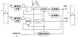
Fig. 3 is a schematic diagram of a dual-input dual-output time difference holding and copying circuit based on a dual-pulse ring oscillator in a related scheme. Fig. 3 shows a dual-input dual-output periodic signal generator that can hold and copy two time domain signals. It is based on the periodic pulse signal generator based on the double-pulse ring oscillator shown in fig. 2, and is formed by combining two pulse generators, two separators (such as separator 1 and separator 2), an alternative multiplexer MUX, and a mode controller. The input end of one pulse generator is IN1, the input end of the other pulse generator is IN2, the output end of the separator 1 is OUT1, the output end of the separator 2 is OUT2, and the control end of the mode controller is # repliica.
Although the dual-input dual-output time difference maintaining and copying circuit based on the dual-pulse ring oscillator shown in fig. 3 can realize maintaining and periodically copying of the time difference of two time-domain signals, the circuit design is complex, and the resource consumption is large. In addition, for a too small time difference between two time domain signals, the circuit cannot realize retention and copy.
Considering that most of the periodic pulse signal generators in the related schemes are single-input single-output, few have dual-input dual-output periodic pulse signal generators. Even in the dual-input dual-output periodic pulse signal generator shown in fig. 3, it is difficult to ensure that the time difference between each pair of output pulses is identical to the time difference between the pair of original input signals, and the circuit cannot realize hold and copy for an excessively small time difference between two time domain signals. Therefore, the invention provides a periodic signal generator, and more particularly, a dual-input dual-output periodic signal generator which is often used in a time difference measurement system, and especially, a periodic pulse signal generating circuit based on a dual-input dual-output ring oscillator (i.e., a periodic pulse signal generator based on a dual-input dual-output ring oscillator), which mainly aims to realize a dual-input dual-output periodic signal generator capable of periodically generating a pair of pulses.
According to an embodiment of the present invention, there is provided a periodic signal generating apparatus. Referring to fig. 4, a schematic diagram of an embodiment of the apparatus of the present invention is shown. The periodic signal generating means may include: the system comprises an input detection unit, a dual-input dual-output annular oscillation unit, a detection output unit, a state detection unit and a control logic unit, wherein the input detection unit is an input detection circuit, the dual-input dual-output annular oscillation unit is a dual-input dual-output annular oscillator, the detection output unit is a detection output circuit, the state detection unit is a state detection circuit, and the control logic unit is a control logic circuit.
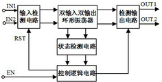
Fig. 5 is a schematic structural diagram of an embodiment of a two-input two-output ring oscillator-based periodic pulse signal generator according to the present invention. As shown in fig. 5, the present invention provides a dual-input dual-output ring oscillator-based periodic pulse signal generator, and in particular, a dual-input dual-output periodic signal generator for periodically generating a pair of pulse signals, including: the system comprises an input detection circuit, a double-input double-output ring oscillator, a detection output circuit, a state detection circuit and a control logic circuit.
Wherein the first input terminal of the input detection circuit and the second input terminal of the input detection circuit are used for inputting external input signals IN1 and IN 2. After passing through the dual-input dual-output ring oscillator, the first output end of the input detection circuit and the second output end of the input detection circuit are correspondingly output to the first input end of the detection output circuit and the second input end of the detection output circuit on the one hand, and are correspondingly input to the second input end of the control logic circuit and the third input end of the control logic circuit after passing through the state detection circuit on the other hand. The first input end of the control logic circuit is used for inputting an enable signal EN. And the first output end of the control logic circuit is output to the third input end of the detection output circuit. And the second output end of the control logic circuit is used for outputting a reset signal to the reset end RST of the input detection circuit. A first output terminal of the detection output circuit and a second output terminal of the detection output circuit for outputting output signals OUT1 and OUT2 corresponding to the external input signal.
In the example shown in fig. 4, the control logic unit is configured to receive an externally input enable signal and send a reset signal to the input detection unit based on the enable signal. Specifically, the control logic unit is configured to receive an enable signal input from the outside and operate based on the enable signal. Wherein the control logic unit, based on the enable signal, comprises: and sending a reset signal to the input detection unit.
In the example shown in fig. 4, the input detection unit is configured to receive a first input signal after reset based on the reset signal, and detect an arrival timing of a rising edge of the first input signal. And receiving a second input signal and detecting the arrival time of the rising edge of the second input signal. The first input signal and the second input signal are external input signals. The input time of the first input signal and the second input signal has a time difference larger than 0.
In the example shown in fig. 5, an input detection circuit is used to detect the arrival of a rising edge of an input signal. The input detection circuit has three input terminals and two output terminals. The first input terminal of the input detection circuit is connected to the external input signal IN1, the second input terminal of the input detection circuit is connected to the external input signal IN2, and the third input terminal of the input detection circuit (i.e., the reset terminal RST of the input detection circuit) is connected to the second output terminal of the control logic circuit. A first output end of the input detection circuit is connected to a first input end of the dual-input dual-output ring oscillator, and a second output end of the input detection circuit is connected to a second input end of the dual-input dual-output ring oscillator.
In some embodiments, the input detection unit includes: a first D flip-flop module and a second D flip-flop module. Of course, the first D flip-flop module may be composed of one D flip-flop, or may be composed of more than two D flip-flops or other flip-flops as long as the function of the D flip-flop is realized. Accordingly, the second D flip-flop module may be composed of one D flip-flop, or may be composed of more than two D flip-flops or other flip-flops as long as the function of the D flip-flop is realized.
The data input end of the first D flip-flop module is connected with a high level signal, the clock input end of the first D flip-flop module is used for inputting the first input signal, the first output end of the first D flip-flop module is output to the first input end of the dual-input dual-output ring oscillator, the first output end of the first D flip-flop module is further output to the first input end of the detection output unit, and the second output end of the first D flip-flop module is output to the control logic unit.
The data input end of the second D trigger module is connected with a high level signal, the clock input end of the second D trigger module is used for inputting the second input signal, the first output end of the second D trigger module is output to the second input end of the double-input double-output ring oscillator, the first output end of the second D trigger module is further output to the second input end of the detection output unit, and the second output end of the second D trigger module is output to the control logic unit.
Fig. 6 is a schematic structural diagram of an embodiment of an input detection circuit, a dual-input dual-output ring oscillator, and a detection output circuit in a periodic pulse signal generator based on a dual-input dual-output ring oscillator according to the present invention. The input detection circuit, the dual-input dual-output ring oscillator and the detection output circuit shown in fig. 6 are a specific circuit example of a periodic pulse signal generator based on a dual-input dual-output ring oscillator provided by the scheme of the present invention. In the following, a specific implementation procedure of the scheme of the present invention will be exemplarily described by taking the circuit shown in fig. 6 as an example, but the implementation manner of the scheme of the present invention is not limited to the specific circuit shown in fig. 6.
In the example shown in fig. 6, the input detection circuit includes: two D flip-flops, such as a first D flip-flop and a second D flip-flop. As the two D flip-flops of the input detection circuit, first input terminals D (i.e., data input terminals) of the two D flip-flops are terminated at a high level, and second input terminals D (i.e., clock input terminals) of the two D flip-flops are connected to the input signals IN1 and IN2, respectively. First output ends Q of the two D triggers are respectively connected to two input ends of the double-input double-output ring oscillator, and second output ends of the two D triggers are connected to the control logic circuit.
In the example shown in fig. 4, the dual-input dual-output ring oscillation unit is configured to copy rising edge information of the first input signal to obtain a first copy signal when the input detection unit detects an arrival timing of a rising edge of the first input signal. And copying the rising edge information of the second input signal to obtain a second copy signal when the input detection unit detects the arrival timing of the rising edge of the second input signal. In a case where the first input signal and the second input signal are periodic signals, the first replica signal and the second replica signal form a first replica pulse signal and a second replica pulse signal.
In the example shown in fig. 5, a dual-input dual-output ring oscillator is used to implement a periodic replica of the two-input rising edges of the first output of the input detection circuit and the second output of the input detection circuit. A dual-input dual-output ring oscillator has two input terminals and four output terminals. The first input end of the dual-input dual-output ring oscillator is connected to the first output end of the input detection circuit, the second input end of the dual-input dual-output ring oscillator is connected to the second output end of the input detection circuit, the first output end of the dual-input dual-output ring oscillator is connected to the first input end of the detection output circuit, the second output end of the dual-input dual-output ring oscillator is connected to the second input end of the detection output circuit, the third output end of the dual-input dual-output ring oscillator is connected to the second input end of the state detection circuit, and the fourth input end of the dual-input dual-output ring oscillator is connected to the first input end of the state detection circuit.
In some embodiments, the dual-input dual-output ring oscillator unit comprises: a dual input dual output ring oscillator.
Wherein, dual input dual output ring oscillator includes: a first delay chain and a second delay chain. The first delay chain and the second delay chain have the same structure, and the first delay chain and the second delay chain are connected end to end.
Specifically, in the scheme of the invention, the dual-input dual-output ring oscillator is formed by connecting an upper delay chain and a lower delay chain which are identical end to end.
In some embodiments, the first delay chain comprises: a first NAND gate module and a first buffer group. The second delay chain, comprising: a second NAND gate module and a second buffer group. Of course, the first nand gate module may be composed of one nand gate, or may be composed of more than two nand gates or other logic devices, as long as the function of the nand gate can be realized. Correspondingly, the second nand gate module may be composed of one nand gate, or may be composed of more than two nand gates or other logic devices, as long as the function of the nand gate can be realized.
And the first input end of the first NAND gate module is connected with the output end of the second buffer group. And the first input end of the first NAND gate module is also connected with the first input end of the detection output unit. And the second input end of the first NAND gate module is connected with the first output end of the input detection unit. And the output end of the first NAND gate module is connected with the second input end of the second NAND gate module after passing through the first buffer group.
And the first input end of the second NAND gate module is connected with the first output end of the input detection unit. And the first input end of the second NAND gate module is also connected with the second input end of the detection output unit. And the first input end of the second NAND gate module is also connected with the first input end of the detection output unit. And the output end of the second NAND gate module is connected with the input end of the second buffer group.
And the output end of the second buffer group is used as the first output end of the double-input double-output oscillation unit. And the second input end of the first NAND gate module is used as the first input end of the dual-input dual-output oscillation unit. And the output end of the first buffer group is used as the second output end of the double-input double-output oscillation unit. And the first input end of the second NAND gate module is used as the second input end of the dual-input dual-output oscillation unit.
Preferably, in the solution of the present invention, each delay chain is formed by a two-input nand gate and a plurality of buffers connected end to end in sequence. The two-input NAND gate is arranged at the forefront and is followed by a series of buffers.
Specifically, the output end of each delay chain is connected to one input end of a two-input and two-output nand gate in another delay chain while being connected to one output end of the detection output circuit as a two-input and two-output ring oscillator, and the other input end of the two-input and two-output nand gate is used as one input end of the two-input and two-output ring oscillator. The dual-input dual-output ring oscillator is connected to a third output end and a fourth output end of the state detection circuit and respectively comes from corresponding positions in an upper delay chain and a lower delay chain of the dual-input dual-output ring oscillator.
In some embodiments, the first buffer group comprises: a first buffer module, the number of the first buffer module being n1, n1 being a positive integer. The second buffer group includes: a second buffer module, the number of the second buffer modules being n2, n2 being a positive integer, and n1 and n2 being the same. Of course, the first buffer module may be one buffer or a module formed by connecting several buffers in series and in parallel, and the second buffer module may be one buffer or a module formed by connecting several buffers in series and in parallel.
Wherein n1 of the first buffer modules are arranged in series and n2 of the second buffer modules are arranged in series. The first delay chain and the second delay chain form a ring oscillator.
And the output end of a buffer is set in the second buffer group and is used as a first phase state detection end of the dual-input dual-output annular oscillation unit. And the output end of a buffer module is set in the first buffer group and is used as a second phase state detection end of the double-input double-output annular oscillation unit.
In the example shown in FIG. 6, a dual-input dual-output ring oscillator includes: the buffer comprises two groups of buffers and two NAND gates, wherein the two groups of buffers comprise a first group of buffers formed by connecting n1 buffers in series and a second group of buffers formed by connecting n2 buffers in series, the two NAND gates comprise a first NAND gate and a second NAND gate, and n1 and n2 are positive integers.
In the scheme of the invention, the periodic pulse generator adopts a dual-input dual-output ring oscillator structure which can ensure that the time difference between any pair of output pulses is accurately equal to the time difference between a pair of signals which are originally input. In the scheme of the invention, the periodic pulse generator adopts the same ring oscillator, so that the periodic pulse generator has the characteristic of good adaptation of the anti-delay unit.
In the example shown in fig. 4, the state detection unit is configured to detect a phase state of the first replica signal when the first replica signal is transmitted on a corresponding transmission chain in the dual-input dual-output ring oscillation unit, so as to obtain a first signal state. And detecting the phase state of the second replica signal when the second replica signal is transmitted on a corresponding transmission chain in the dual-input dual-output annular oscillation unit to obtain a second signal state.
In the example shown in fig. 5, the state detection circuit is used to detect the phase state of the transmission signal on the upper and lower delay chains of the dual-input dual-output ring oscillator. The state detection circuit has two input terminals and two output terminals. The first input end of the state detection circuit is connected to the fourth output end of the dual-input dual-output ring oscillator, the second input end of the state detection circuit is connected to the third output end of the dual-input dual-output ring oscillator, the first output end of the state detection circuit is connected to the second input end of the control logic circuit, and the second output end of the state detection circuit is connected to the third input end of the control logic circuit.
In some embodiments, the state detection unit includes: the device comprises a first state detection module and a second state detection module.
The first state detection module and the second state detection module have the same structure, the first state detection module is arranged between a first phase state detection end of the dual-input dual-output annular oscillation unit and the control logic unit, and the second state detection module is arranged between a second phase state detection end of the dual-input dual-output annular oscillation unit and the control logic unit.
In the scheme of the invention, the state detection circuit is used for detecting the phase change condition of a signal at a certain position on the upper delay chain and the lower delay chain of the dual-input dual-output ring oscillator. The state detection circuit can be implemented in various forms.
In some embodiments, the first state detection module, in some embodiments, comprises: the buffer comprises a first inverter module and a third buffer group, wherein the third buffer group is formed by connecting m1 buffer modules in series, and m1 is a positive integer. The second state detection module includes: the buffer comprises a second inverter module and a fourth buffer group, wherein the fourth buffer group is formed by connecting m2 buffer modules in series, m2 is a positive integer, and m1 and m2 are the same. Of course, the first inverter block may be formed by one inverter, or may be formed by two or more inverters or other logic devices as long as the function of the inverter is realized. Accordingly, the second inverter module may be composed of one inverter, or may be composed of two or more inverters or other logic devices as long as the function of the inverter is realized.
The input end of the first phase inverter module is connected with the first phase state detection end of the double-input double-output annular oscillation unit. And the output end of the first phase inverter module is connected with the second input end of the control logic unit after passing through the third buffer group.
And the input end of the second phase inverter module is connected with the second phase state detection end of the double-input double-output annular oscillation unit. And the output end of the second phase inverter module is connected with the third input end of the control logic unit after passing through the fourth buffer group.
And the first input end of the control logic unit is used for inputting the enabling signal. And the second output end of the control logic unit is used for outputting the reset signal. And the first output end of the control logic unit is used for outputting the number of the current periods of the first replica signal and the second replica signal and the size of each current period.
Fig. 7 is a schematic structural diagram of an embodiment of a state detection circuit and a logic control circuit in a periodic pulse signal generator based on a dual-input dual-output ring oscillator according to the present invention. As shown in fig. 7, the state detection circuit may be formed by an inverter and a plurality of delay units.
In the example shown in fig. 4, the control logic unit is further configured to determine the number of current cycles of the first replica signal and the second replica signal and the size of each current cycle according to the first signal state and the second signal state based on the enable signal. Specifically, the control logic unit, operating based on the enable signal, further includes: and determining the number of cycles of the first replica signal and the second replica signal and the size of each cycle according to the first signal state and the second signal state.
In the example shown in fig. 5, the control logic circuit is used to control the number of cycles and the size of the two output periodic pulse signals. The control logic circuit has three input terminals and two output terminals. The first input end of the control logic circuit is connected with the external enable signal EN, the second input end of the control logic circuit is connected to the first output end of the state detection circuit, the third input end of the control logic circuit is connected to the second output end of the state detection circuit, the second output end of the control logic circuit is connected to the third input end of the input detection circuit, and the first output end of the control logic circuit is connected to the third input end of the detection output circuit.
In some embodiments, the control logic unit comprises: a counter-based logic processing module. And the logic processing module based on the counter is respectively connected with the input detection unit, the state detection unit and the detection output unit.
In the scheme of the invention, the control logic circuit is used for realizing the control of the output pulse period and the pulse number. The implementation form of the logic control circuit can be various forms. For example: and the control logic circuit can be realized by a logic circuit based on a counter.
In some embodiments, the control logic unit comprises: the buffer comprises a third D trigger module, a fourth D trigger module, a fifth buffer group, a third NAND gate module, a fourth NAND gate module and a third AND gate module. The fifth buffer group is formed by connecting m3 buffer modules in series, and m3 is a positive integer.
And the clock input end of the third D trigger module is connected with the first output end of the state detection unit. And the data input end of the third D trigger module is respectively connected with the second output end of the third D trigger module, the clock input end of the fourth D trigger module and the clock input end of the fifth D trigger module. And the reset end of the third D trigger module is respectively connected with the reset end of the fourth D trigger module, the reset end of the fifth D trigger module and the output end of the fourth NAND module. And the first output end of the third D trigger module is respectively connected with the input end of the fifth buffer group and the first input end of the third NAND gate module. And the output end of the fifth buffer group is connected with the detection output unit.
And the data input end of the fourth D trigger module is respectively connected with the second output end of the fourth D trigger module and the second input end of the third NAND gate module. And the first output end of the fourth D trigger module is connected with the data input end of the fifth D trigger module.
And the first output end of the fifth D flip-flop module is connected with the third input end of the third NAND gate module. And the output end of the third NAND gate module is connected with the second input end of the third AND gate module. And the first input end of the third AND gate module is used for inputting the enabling signal. And the output end of the third AND gate module is connected with the reset end of the input detection unit.
And the first input end of the fourth NAND gate module is connected with the second output end of the state detection unit. And the second input end of the fourth NAND gate module is connected with the second output end of the input detection unit. The second output terminal of the input detection unit is the second output terminal of the second D flip-flop.
And the clock input end of the third D trigger module is used as the second input end of the control logic unit. And the first input end of the fourth NAND gate module is used as the third input end of the control logic unit. And the first input end of the third AND gate module is used as the first input end of the control logic unit. And the output end of the third AND gate module is used as a second output end of the control logic unit. And the output end of the fifth buffer group is used as the first output end of the control logic unit.
The two-input two-output ring oscillator based periodic pulse signal generator shown in fig. 7 can control the output pulse number of pairs to be 2, and the pulse period is twice as long as that of the two-input two-output ring oscillator.
In the scheme of the invention, the periodic pulse generator also adopts a control logic circuit, and through reasonable control, on one hand, the period size of the output signal can be changed by integral multiple, and on the other hand, the number of the output pulses can be flexibly controlled.
In the example shown in fig. 4, the detection output unit is configured to output the first replica signal and the second replica signal, which are denoted as a first pulse signal and a second pulse signal, according to the number of current cycles of the first replica signal and the second replica signal and the size of each current cycle, so as to generate the first pulse signal and the second pulse signal with dual outputs based on the first input signal and the second input signal with dual inputs. Wherein a time difference between the first pulse signal and the second pulse signal is the same as a time difference between the first input signal and the second input signal.
In the example shown in FIG. 5, a sense output circuit is used to sense the periodic pulse signal output by the dual input, dual output ring oscillator. The detection output circuit is provided with three input ends and two output ends. The first input end of the detection output circuit is connected to the first output end of the dual-input dual-output ring oscillator, the second input end of the detection output circuit is connected to the second output end of the dual-input dual-output ring oscillator, the third input end of the detection output circuit is connected to the first output end of the control logic circuit, the first output end of the detection output circuit is connected to the first signal output end for outputting a signal OUT1 (namely, an output signal Y1), and the second output end of the detection output circuit is connected to the second signal output end for outputting a signal OUT2 (namely, an output signal Y2).
The scheme of the invention provides a periodic pulse signal generating circuit based on a dual-input dual-output ring oscillator (namely, the periodic pulse signal generator based on the dual-input dual-output ring oscillator), which not only can periodically generate a pair of pulse dual-input dual-output periodic signal generators, but also the time difference between each pair of output pulses is completely the same as the time difference between the original pair of input signals, and is not limited by the minimum input time difference, so that the application range of the periodic pulse signal generator is greatly improved.
In some embodiments, the detection output unit includes: the first AND gate module and the second AND gate module. Of course, the first and gate module may be formed by one and gate, or may be formed by more than two and gates or other logic devices, as long as the function of the and gate can be realized. Correspondingly, the second and gate module may be formed by one and gate, or may be formed by more than two and gates or other logic devices, as long as the function of the and gate can be realized.
The first input end of the first and gate module is used as the first input end of the detection output unit and is connected with the first output end of the dual-input dual-output annular oscillation unit. And the second input end of the first AND gate module is respectively connected with the first output end of the input detection unit and the first input end of the dual-input dual-output annular oscillation unit. And the third input end of the first AND gate module is connected with the control logic unit. And the output end of the first AND gate module is used for outputting the first pulse signal.
And the first input end of the second AND gate module is used as the first input end of the detection output unit and is connected with the second output end of the dual-input dual-output annular oscillation unit. And the second input end of the second AND gate module is respectively connected with the second output end of the input detection unit and the second input end of the dual-input dual-output annular oscillation unit. And the third input end of the second AND gate module is connected with the control logic unit. And the output end of the second AND gate module is used for outputting the second pulse signal.
In the example shown in fig. 6, the detection output circuit includes: two three-input and gates, such as a first and gate and a second and gate. The first output ends Q of the two D triggers serving as the input detection circuit are also respectively connected to the second input ends of two three-input AND gates in the detection output circuit.
Specifically, a first input terminal D (i.e., a data input terminal) of the first D flip-flop is terminated with a high level, a second input terminal (i.e., a clock input terminal) of the first D flip-flop is connected to the external input signal IN1, a first output terminal Q of the first D flip-flop is connected to a second input terminal of the first nand gate, the first output terminal Q of the first D flip-flop is further connected to a second input terminal of the first and gate, a reset terminal, i.e., an R terminal, of the first D flip-flop is connected to the control logic circuit, and a Q non-terminal of the first D flip-flop is connected to the control logic circuit.
A first input end D (i.e., a data input end) of the second D flip-flop is terminated with a high level, a second input end (i.e., a clock input end) of the second D flip-flop is connected with an external input signal IN2, a first output end Q of the second D flip-flop is connected to a first input end of the second nand gate, the first output end Q of the second D flip-flop is further connected to a second input end of the second and gate, a reset end (i.e., an R end) of the second D flip-flop is connected to the control logic circuit, and a Q end of the second D flip-flop is connected to the control logic circuit.
The first input end of the first AND gate is connected to the first input end of the first NAND gate, the third input end of the first AND gate is connected to the control logic circuit, and the output end of the first AND gate is used for outputting a signal OUT 1. The first input end of the first NAND gate is also connected to the output ends of the second group of buffers. The output end of the first NAND gate is connected to the second input end of the second NAND gate after passing through the first group of buffers. The output end of the first NAND gate is connected to the second input end of the second AND gate after passing through the first group of buffers. The third input terminal of the second and gate is connected to the control logic circuit, and the output terminal of the second and gate is used for outputting the signal OUT 2. The output end of the second NAND gate is connected to the first input end of the first NAND gate after passing through the second group of buffers.
Referring to the examples shown in fig. 5, 6 and 7, the first input terminal of the control logic circuit is connected to the external enable control signal EN. Before the periodic pulse signal generator works, the enable signal EN is always at a low potential. Before the periodic pulse signal generator works normally, the third input ends (namely reset ends R) of the two D triggers for detecting the input signals are at a low potential, so that the first output ends Q of the two D triggers are at a low potential state. Before the dual-input dual-output ring oscillator works normally, two input ends of the dual-input dual-output ring oscillator are both low levels, so that initial output states of any delay units (such as a buffer, a dual-input NAND gate and the like) on the dual-input dual-output ring oscillator are both high levels.
In specific implementation, after the enable signal EN changes to a high level, the control logic circuit starts to operate, and the first output end and the fourth output end of the control logic circuit both change from a low level to a high level, so that the two D flip-flops for detecting the input signal also enter an enable state. Then, when an input signal such as IN1 (or IN 2) arrives, the first output Q of the D flip-flop IN the corresponding input signal detection circuit goes high, so that the output of the following two-input nand gate goes from high to low, and the two-input nand gate is equivalent to a not gate. The low level propagates all the way along the corresponding lower (or upper) delay chain in the dual-input dual-output ring oscillator. Before the low level propagates to the end of the delay chain, another input signal IN2 (or IN 1) comes to the input of another detection circuit.
With the arrival of the other input signal IN2 (or IN 1), the first output Q of the other input signal detecting circuit D flip-flop also changes from low level to high level, so that the output of the following two-input nand gate also changes from high level to low level, and the two-input nand gate also becomes an inverter. The low level also propagates all the way along the corresponding upper (lower) delay chain in the dual-input dual-output ring oscillator.
When the low level introduced by the previous input IN1 (or IN 2) propagates to the end of the delay chain below (or above) it is, then at the next moment, the low level IN the lower (or above) delay chain will transition to the high level IN the upper delay chain, since a low level also appears on the other delay chain at that moment. The low level also introduced by the latter input IN2 (or IN 1) will also transition to a low level IN the lower (or upper) delay chain at the next moment when it propagates to the end of the upper (or lower) delay chain IN which it is located.
When the low level in the upper and lower delay chains of the dual-input dual-output ring oscillator is respectively transmitted to the other delay chain, the low level is correspondingly changed into the high level. When the two high levels are transmitted back to the previous delay chain, the two high levels become low levels again. Through the repeated change, two periodic signals with constant relative distance are formed on the dual-input dual-output ring oscillator.
The first output end Q of the two D flip-flops for detecting the input signal is kept at a high potential all the time after the input signal is detected. The control logic circuit determines the output signal states of the second and third output terminals connected to the three input and gate third input terminals according to the preset setting. When the second and third output terminals of the control logic circuit are at low level, the outputs of the two three-input and gates are always at low level, and the periodic signal on the dual-input dual-output ring oscillator cannot be guided out. When the second and third output terminals of the control logic circuit are at high level, the two three-input and gates will transmit the signals at the first and second output terminals of the dual-input dual-output ring oscillator to the output terminals OUT1 and OUT2, respectively.
Of course, the control logic circuit may also make the second and third output terminals periodically exhibit high and low levels according to the previous setting, so as to change the output signal period of the periodic pulse signal generator and the number of output pulse periods.
When the enable signal EN changes to a low level, the first and fourth output terminals of the control logic circuit output a low level, so that the two D flip-flops are in a reset state. And then the dual-input dual-output ring oscillator also stops oscillating, and the output of each delay unit on the dual-input dual-output ring oscillator returns to the high potential of the initial state.
Fig. 8 is a schematic diagram of input and output signal waveforms of a periodic pulse signal generator based on a dual-input dual-output ring oscillator according to the present invention. Fig. 8 shows a schematic diagram of input-output signal waveforms of a periodic pulse signal generator based on a dual-input dual-output ring oscillator.
In summary, the scheme of the invention provides a periodic pulse signal generator based on a dual-input dual-output ring oscillator, which is capable of periodically generating a pair of output pulse signals, and the time difference between each pair of output pulse signals is completely equal to the time difference between the pair of signals originally input. In addition, the periodic pulse signal generator simultaneously adopts a state detection circuit and a control logic circuit, so that the period size of the output pulse can be adjusted in integral multiple, and the period number of the output pulse can be flexibly adjusted. The periodic pulse signal generator can periodically copy the difference value of any two time domain signals with the time difference not larger than half of the oscillation period, so that the periodic pulse signal generator can be well applied to the application environment needing to measure the time difference of two input signals for multiple times.
By adopting the technical scheme of the invention, the periodic pulse signal generating device is arranged based on the dual-input dual-output ring oscillator (such as a dual-input dual-output ring oscillator) to realize that a pair of output pulse signals are periodically output, and the time difference between each pair of output pulse signals is completely the same as the time difference between the original pair of input signals and is not limited by the minimum input time difference, so that the application range of the periodic pulse signal generator can be expanded by arranging the periodic pulse signal generating device capable of generating a pair of pulse signals.
According to the embodiment of the invention, a signal processing system corresponding to the periodic signal generating device, namely a signal processing system (such as a signal measuring system, a signal calibrating system and the like) with a double periodic pulse signal generator is also provided. The signal processing system may include: the above-mentioned periodic signal generating device.
Since the processing and functions implemented by the signal processing system of this embodiment basically correspond to the embodiments, principles and examples of the apparatus, reference may be made to the related descriptions in the foregoing embodiments without being detailed in the description of this embodiment.
By adopting the technical scheme of the embodiment, the periodic pulse signal generating device is arranged based on the dual-input dual-output ring oscillator device (such as a dual-input dual-output ring oscillator), so that a pair of output pulse signals are periodically output, and the time difference between each pair of output pulse signals is completely the same as the time difference between an original pair of input signals and is not limited by the minimum input time difference, wherein the dual-input dual-output ring oscillator can ensure that the time difference between any pair of generated output pulses is accurately equal to the time difference between the pair of signals which are originally input, so that the accuracy of the time difference between any pair of output pulses is better.
According to an embodiment of the present invention, a periodic signal generating method of a signal processing system corresponding to the signal processing system is also provided, as shown in fig. 9, which is a schematic flowchart of an embodiment of the method of the present invention. The periodic signal generating method of the signal processing system may include: step S110 to step S160.
At step S110, the control logic unit is controlled, receives an externally input enable signal, and transmits a reset signal to the input detection unit based on the enable signal.
At step S120, controlling the input detection unit to receive a first input signal after reset based on the reset signal, and detecting an arrival timing of a rising edge of the first input signal; and receiving a second input signal and detecting the arrival time of the rising edge of the second input signal.
At step S130, controlling the dual-input dual-output ring oscillation unit, and copying rising edge information of the first input signal to obtain a first copied signal when the input detection unit detects an arrival timing of a rising edge of the first input signal; and copying the rising edge information of the second input signal to obtain a second copy signal when the input detection unit detects the arrival timing of the rising edge of the second input signal.
At step S140, controlling the state detection unit to detect a phase state of the first replica signal when the first replica signal is transmitted on a corresponding transmission chain in the dual-input dual-output ring oscillation unit, so as to obtain a first signal state; and detecting the phase state of the second replica signal when the second replica signal is transmitted on a corresponding transmission chain in the dual-input dual-output annular oscillation unit to obtain a second signal state.
At step S150, the control logic unit is controlled to determine the number of current cycles of the first replica signal and the second replica signal and the size of each current cycle according to the first signal state and the second signal state based on the enable signal.
At step S160, controlling the detection output unit to output the first replica signal and the second replica signal, which are denoted as a first pulse signal and a second pulse signal, according to the number of current cycles of the first replica signal and the second replica signal and the size of each current cycle, so as to generate the first pulse signal and the second pulse signal with dual outputs based on the first input signal and the second input signal with dual inputs. Wherein a time difference between the first pulse signal and the second pulse signal is the same as a time difference between the first input signal and the second input signal.
The scheme of the invention provides a periodic pulse signal generating mode based on a dual-input dual-output ring oscillator (namely, the periodic pulse signal generating mode based on the periodic pulse signal generator of the dual-input dual-output ring oscillator), which not only can periodically generate a pair of pulse dual-input dual-output periodic signal generators, but also the time difference between each pair of output pulses is completely the same as the time difference between the original pair of input signals, and is not limited by the minimum input time difference, thereby greatly improving the application range of the periodic pulse signal generators.
Since the processing and functions implemented by the method of the present embodiment substantially correspond to the embodiments, principles, and examples of the signal processing system, reference may be made to the related descriptions in the foregoing embodiments without being detailed in the description of the present embodiment.
By adopting the technical scheme of the embodiment, the periodic pulse signal generation modes of the signal processing systems such as the signal measurement system and the signal calibration system are set based on the dual-input dual-output ring oscillator (such as the dual-input dual-output ring oscillator), so that the pair of output pulse signals can be periodically output, the time difference between each pair of output pulse signals is completely the same as the time difference between the original pair of input signals, the limitation of the minimum input time difference is avoided, the method is accurate and reliable, and the implementation mode is simple.
In conclusion, it is readily understood by those skilled in the art that the advantageous modes described above can be freely combined and superimposed without conflict.
The above description is only an example of the present invention, and is not intended to limit the present invention, and it is obvious to those skilled in the art that various modifications and variations can be made in the present invention. Any modification, equivalent replacement, or improvement made within the spirit and principle of the present invention should be included in the scope of the claims of the present invention.
Claims (10)
1. A periodic signal generating apparatus, comprising: the system comprises an input detection unit, a double-input double-output annular oscillation unit, a detection output unit, a state detection unit and a control logic unit; wherein the content of the first and second substances,
the control logic unit is configured to receive an enable signal input from the outside and send a reset signal to the input detection unit based on the enable signal;
the input detection unit is configured to receive a first input signal after reset based on the reset signal, and detect the arrival timing of the rising edge of the first input signal; receiving a second input signal and detecting the arrival time of the rising edge of the second input signal;
the dual-input dual-output annular oscillation unit is configured to copy rising edge information of the first input signal to obtain a first copy signal under the condition that the input detection unit detects arrival time of the rising edge of the first input signal; under the condition that the input detection unit detects the arrival time of the rising edge of the second input signal, copying the rising edge information of the second input signal to obtain a second copy signal;
the state detection unit is configured to detect a phase state of the first replica signal when the first replica signal is transmitted on a corresponding transmission chain in the dual-input dual-output annular oscillation unit, so as to obtain a first signal state; detecting the phase state of the second replica signal when the second replica signal is transmitted on a corresponding transmission chain in the dual-input dual-output annular oscillation unit to obtain a second signal state;
the control logic unit is further configured to determine the number of current cycles of the first replica signal and the second replica signal and the size of each current cycle according to the first signal state and the second signal state based on the enable signal;
the detection output unit is configured to output the first replica signal and the second replica signal according to the number of current cycles of the first replica signal and the second replica signal and the size of each current cycle, and to generate the first pulse signal and the second pulse signal with dual outputs based on the first input signal and the second input signal with dual inputs.
2. The periodic signal generation apparatus according to claim 1, wherein the input detection unit includes: a first D flip-flop module and a second D flip-flop module; wherein the content of the first and second substances,
a data input end of the first D flip-flop module is connected to a high level signal, a clock input end of the first D flip-flop module is used for inputting the first input signal, a first output end of the first D flip-flop module is output to a first input end of the dual-input dual-output ring oscillator, a first output end of the first D flip-flop module is also output to a first input end of the detection output unit, and a second output end of the first D flip-flop module is output to the control logic unit;
the data input end of the second D trigger module is connected with a high level signal, the clock input end of the second D trigger module is used for inputting the second input signal, the first output end of the second D trigger module is output to the second input end of the double-input double-output ring oscillator, the first output end of the second D trigger module is further output to the second input end of the detection output unit, and the second output end of the second D trigger module is output to the control logic unit.
3. The periodic signal generation device of claim 1, wherein the dual-input dual-output ring oscillator unit comprises: a dual-input dual-output ring oscillator;
wherein, dual input dual output ring oscillator includes: a first delay chain and a second delay chain; the first delay chain and the second delay chain have the same structure, and the first delay chain and the second delay chain are connected end to end.
4. The periodic signal generation device of claim 3, wherein the first delay chain comprises: a first nand gate module and a first buffer group; the second delay chain, comprising: a second nand gate module and a second buffer group;
the first input end of the first NAND gate module is connected with the output end of the second buffer group; the first input end of the first NAND gate module is also connected with the first input end of the detection output unit; the second input end of the first NAND gate module is connected with the first output end of the input detection unit; the output end of the first NAND gate module is connected with the second input end of the second NAND gate module after passing through the first buffer group;
the first input end of the second NAND gate module is connected with the first output end of the input detection unit; the first input end of the second NAND gate module is also connected with the second input end of the detection output unit; the first input end of the second NAND gate module is also connected with the first input end of the detection output unit; the output end of the second NAND gate module is connected with the input end of the second buffer group;
the output end of the second buffer group is used as the first output end of the dual-input dual-output oscillation unit; a second input end of the first NAND gate module is used as a first input end of the dual-input dual-output oscillation unit; the output end of the first buffer group is used as a second output end of the double-input double-output oscillation unit; and the first input end of the second NAND gate module is used as the second input end of the dual-input dual-output oscillation unit.
5. The periodic signal generation apparatus of claim 4, wherein the first buffer group comprises: a number of first buffer modules being n1, n1 being a positive integer; the second buffer group includes: a second buffer module, the number of the second buffer module being n2, n2 being a positive integer, and n1 and n2 being the same;
wherein n1 of the first buffer modules are arranged in series and n2 of the second buffer modules are arranged in series; the first delay chain and the second delay chain form a ring oscillator;
the output end of a buffer is set in the second buffer group and is used as a first phase state detection end of the double-input double-output annular oscillation unit; and the output end of a buffer module is set in the first buffer group and is used as a second phase state detection end of the double-input double-output annular oscillation unit.
6. The periodic signal generation device according to claim 1, wherein the detection output unit includes: the first AND gate module and the second AND gate module;
a first input end of the first and gate module is used as a first input end of the detection output unit and is connected with a first output end of the dual-input dual-output annular oscillation unit; the second input end of the first AND gate module is respectively connected with the first output end of the input detection unit and the first input end of the dual-input dual-output annular oscillation unit; the third input end of the first AND gate module is connected with the control logic unit; the output end of the first AND gate module is used for outputting the first pulse signal;
the first input end of the second AND gate module is used as the first input end of the detection output unit and is connected with the second output end of the double-input double-output annular oscillation unit; the second input end of the second AND gate module is respectively connected with the second output end of the input detection unit and the second input end of the dual-input dual-output annular oscillation unit; the third input end of the second AND gate module is connected with the control logic unit; and the output end of the second AND gate module is used for outputting the second pulse signal.
7. The periodic signal generation apparatus according to any one of claims 1 to 6, wherein,
the state detection unit includes: the device comprises a first state detection module and a second state detection module; wherein the content of the first and second substances,
the first state detection module and the second state detection module have the same structure, the first state detection module is arranged between a first phase state detection end of the dual-input dual-output annular oscillation unit and the control logic unit, and the second state detection module is arranged between a second phase state detection end of the dual-input dual-output annular oscillation unit and the control logic unit;
and/or the presence of a gas in the gas,
the control logic unit comprises: a counter-based logic processing module; and the logic processing module based on the counter is respectively connected with the input detection unit, the state detection unit and the detection output unit.
8. The periodic signal generation apparatus of claim 7, wherein,
the first state detection module includes: the buffer comprises a first inverter module and a third buffer group, wherein the third buffer group is formed by connecting m1 buffer modules in series, and m1 is a positive integer; the second state detection module includes: the buffer comprises a second inverter module and a fourth buffer group, wherein the fourth buffer group is formed by connecting m2 buffer modules in series, m2 is a positive integer, and m1 is the same as m 2; wherein the content of the first and second substances,
the input end of the first phase inverter module is connected with the first phase state detection end of the double-input double-output annular oscillation unit; the output end of the first inverter module is connected with the second input end of the control logic unit after passing through the third buffer group;
the input end of the second phase inverter module is connected with the second phase state detection end of the double-input double-output annular oscillation unit; the output end of the second inverter module is connected with the third input end of the control logic unit after passing through the fourth buffer group;
the first input end of the control logic unit is used for inputting the enabling signal; the second output end of the control logic unit is used for outputting the reset signal; a first output end of the control logic unit, configured to output the number of current cycles of the first replica signal and the second replica signal, and the size of each current cycle;
and/or the presence of a gas in the gas,
the control logic unit comprises: the buffer comprises a third D trigger module, a fourth D trigger module, a fifth buffer group, a third NAND gate module, a fourth NAND gate module and a third AND gate module; the fifth buffer group is formed by connecting m3 buffer modules in series, and m3 is a positive integer; wherein the content of the first and second substances,
the clock input end of the third D trigger module is connected with the first output end of the state detection unit; the data input end of the third D flip-flop module is connected to the second output end of the third D flip-flop module, the clock input end of the fourth D flip-flop module, and the clock input end of the fifth D flip-flop module, respectively; the reset end of the third D flip-flop module is connected to the reset end of the fourth D flip-flop module, the reset end of the fifth D flip-flop module, and the output end of the fourth nand module, respectively; a first output end of the third D flip-flop module is connected to an input end of the fifth buffer group and a first input end of the third nand gate module, respectively; the output end of the fifth buffer group is connected with the detection output unit;
the data input end of the fourth D flip-flop module is connected to the second output end of the fourth D flip-flop module and the second input end of the third nand gate module, respectively; the first output end of the fourth D trigger module is connected with the data input end of the fifth D trigger module;
a first output end of the fifth D flip-flop module is connected to a third input end of the third nand gate module; the output end of the third NAND gate module is connected with the second input end of the third AND gate module; the first input end of the third and gate module is used for inputting the enable signal; the output end of the third AND gate module is connected with the reset end of the input detection unit;
the first input end of the fourth NAND gate module is connected with the second output end of the state detection unit; the second input end of the fourth NAND gate module is connected with the second output end of the input detection unit;
a clock input end of the third D flip-flop module is used as a second input end of the control logic unit; the first input end of the fourth NAND gate module is used as the third input end of the control logic unit; a first input end of the third and gate module is used as a first input end of the control logic unit; the output end of the third AND gate module is used as the second output end of the control logic unit; and the output end of the fifth buffer group is used as the first output end of the control logic unit.
9. A signal processing system, comprising: a periodic signal generation device according to any one of claims 1 to 8.
10. A periodic signal generation method of a signal processing system according to claim 9, comprising:
the control logic unit is controlled to receive an enable signal input from the outside and send a reset signal to the input detection unit based on the enable signal;
controlling the input detection unit to receive a first input signal after reset based on the reset signal and detect arrival timing of a rising edge of the first input signal; receiving a second input signal and detecting the arrival time of the rising edge of the second input signal;
controlling the dual-input dual-output annular oscillation unit, and copying rising edge information of the first input signal to obtain a first copy signal under the condition that the input detection unit detects arrival time of the rising edge of the first input signal; under the condition that the input detection unit detects the arrival time of the rising edge of the second input signal, copying the rising edge information of the second input signal to obtain a second copy signal;
controlling the state detection unit to detect a phase state of the first replica signal when the first replica signal is transmitted on a corresponding transmission chain in the dual-input dual-output annular oscillation unit to obtain a first signal state; detecting the phase state of the second replica signal when the second replica signal is transmitted on a corresponding transmission chain in the dual-input dual-output annular oscillation unit to obtain a second signal state;
controlling the control logic unit to determine the number of current cycles of the first replica signal and the second replica signal and the size of each current cycle according to the first signal state and the second signal state based on the enable signal;
and controlling the detection output unit to output the first replica signal and the second replica signal according to the number of current cycles of the first replica signal and the second replica signal and the size of each current cycle, wherein the first replica signal and the second replica signal are recorded as a first pulse signal and a second pulse signal, and the first pulse signal and the second pulse signal with double outputs are generated based on the first input signal and the second input signal with double inputs.
Priority Applications (1)
| Application Number | Priority Date | Filing Date | Title |
|---|---|---|---|
| CN202210595557.9A CN114679158B (en) | 2022-05-30 | 2022-05-30 | Periodic signal generating device, signal processing system and periodic signal generating method thereof |
Applications Claiming Priority (1)
| Application Number | Priority Date | Filing Date | Title |
|---|---|---|---|
| CN202210595557.9A CN114679158B (en) | 2022-05-30 | 2022-05-30 | Periodic signal generating device, signal processing system and periodic signal generating method thereof |
Publications (2)
| Publication Number | Publication Date |
|---|---|
| CN114679158A CN114679158A (en) | 2022-06-28 |
| CN114679158B true CN114679158B (en) | 2022-08-05 |
Family
ID=82080135
Family Applications (1)
| Application Number | Title | Priority Date | Filing Date |
|---|---|---|---|
| CN202210595557.9A Active CN114679158B (en) | 2022-05-30 | 2022-05-30 | Periodic signal generating device, signal processing system and periodic signal generating method thereof |
Country Status (1)
| Country | Link |
|---|---|
| CN (1) | CN114679158B (en) |
Citations (4)
| Publication number | Priority date | Publication date | Assignee | Title |
|---|---|---|---|---|
| CN103427795A (en) * | 2013-08-12 | 2013-12-04 | 中国航天科技集团公司第九研究院第七七一研究所 | Matrix pulse signal generation circuit and generation method |
| CN105656456A (en) * | 2014-11-30 | 2016-06-08 | 中国科学院沈阳自动化研究所 | High-speed and high-precision digital pulse generating circuit and pulse generating method |
| CN112118007A (en) * | 2019-06-21 | 2020-12-22 | 爱思开海力士有限公司 | Phase detection circuit, clock generation circuit, and semiconductor device |
| CN112615589A (en) * | 2020-12-15 | 2021-04-06 | 海光信息技术股份有限公司 | Method and device for adjusting frequency of ring oscillator, storage medium and equipment |
Family Cites Families (2)
| Publication number | Priority date | Publication date | Assignee | Title |
|---|---|---|---|---|
| KR102279606B1 (en) * | 2017-10-26 | 2021-07-21 | 에스케이하이닉스 주식회사 | Duty cycle detector and phase differnece detector |
| US10483953B2 (en) * | 2018-02-07 | 2019-11-19 | Texas Instruments Incorporated | Ring oscillator-based timer |
-
2022
- 2022-05-30 CN CN202210595557.9A patent/CN114679158B/en active Active
Patent Citations (4)
| Publication number | Priority date | Publication date | Assignee | Title |
|---|---|---|---|---|
| CN103427795A (en) * | 2013-08-12 | 2013-12-04 | 中国航天科技集团公司第九研究院第七七一研究所 | Matrix pulse signal generation circuit and generation method |
| CN105656456A (en) * | 2014-11-30 | 2016-06-08 | 中国科学院沈阳自动化研究所 | High-speed and high-precision digital pulse generating circuit and pulse generating method |
| CN112118007A (en) * | 2019-06-21 | 2020-12-22 | 爱思开海力士有限公司 | Phase detection circuit, clock generation circuit, and semiconductor device |
| CN112615589A (en) * | 2020-12-15 | 2021-04-06 | 海光信息技术股份有限公司 | Method and device for adjusting frequency of ring oscillator, storage medium and equipment |
Also Published As
| Publication number | Publication date |
|---|---|
| CN114679158A (en) | 2022-06-28 |
Similar Documents
| Publication | Publication Date | Title |
|---|---|---|
| US5764710A (en) | Meta-stable-resistant front-end to a synchronizer with asynchronous clear and asynchronous second-stage clock selector | |
| US5036230A (en) | CMOS clock-phase synthesizer | |
| US6906555B2 (en) | Prevention of metastability in bistable circuits | |
| US8453043B2 (en) | Built-in bit error rate test circuit | |
| CN110311659B (en) | Trigger and integrated circuit | |
| KR20030091015A (en) | Internal clock signal generating circuit and method | |
| CN102362432A (en) | Low-power dual-edge-triggered storage cell with scan test support and clock gating circuit therefor | |
| KR890017866A (en) | Filter circuit | |
| US6362694B1 (en) | Method and apparatus for providing a ring oscillator | |
| JP2005244479A (en) | Transmission apparatus | |
| US10530348B2 (en) | Shift register utilizing latches controlled by dual non-overlapping clocks | |
| US6509775B2 (en) | Synchronous delay circuit and semiconductor integrated circuit apparatus | |
| JP2003008414A (en) | Clock edge detection circuit | |
| US7233543B2 (en) | System and method to change data window | |
| US4949360A (en) | Synchronizing circuit | |
| CN114679158B (en) | Periodic signal generating device, signal processing system and periodic signal generating method thereof | |
| KR20210054651A (en) | Timing data acquisition device | |
| US20100237918A1 (en) | Frequency measuring circuit and semiconductor device having the same | |
| JP5413216B2 (en) | Delay time difference measurement circuit | |
| US7400178B2 (en) | Data output clock selection circuit for quad-data rate interface | |
| CN109660232B (en) | Pulse trigger circuit | |
| US6166574A (en) | Circuit for turning on and off a clock without a glitch | |
| KR100305027B1 (en) | Retarder | |
| US10158351B1 (en) | Skew control apparatus and algorithm using a low pass filter | |
| WO2023033103A1 (en) | Successive-approximation register based a/d converter |
Legal Events
| Date | Code | Title | Description |
|---|---|---|---|
| PB01 | Publication | ||
| PB01 | Publication | ||
| SE01 | Entry into force of request for substantive examination | ||
| SE01 | Entry into force of request for substantive examination | ||
| GR01 | Patent grant | ||
| GR01 | Patent grant |