Detailed Description
The following disclosure provides many different embodiments, or examples, for implementing different features of the invention. Specific examples of components and arrangements are described below to simplify the present disclosure. Of course, these are merely examples and are not intended to be limiting. For example, forming a first feature over or on a second feature in the description that follows may include embodiments in which the first and second features are formed in direct contact, and may also include embodiments in which additional features may be formed between the first and second features, such that the first and second features may not be in direct contact.
Furthermore, spatially relative terms (e.g., "below," "beneath," "below," "over," "upper," and the like) may be used herein to readily describe one element or feature's relationship to another element(s) or feature(s) as illustrated in the figures. These spatially relative terms are intended to encompass different orientations of the device in use or operation in addition to the orientation depicted in the figures. The device may be otherwise oriented (rotated 90 degrees or at other orientations) and the spatially relative descriptors used herein interpreted accordingly. Throughout the description herein, the same or similar reference numbers in different figures refer to the same or similar elements formed by the same or similar forming methods using the same or similar material(s), unless otherwise specified. Moreover, unless otherwise noted, figures having the same number and different letters (e.g., fig. 8A and 8B) illustrate different views (e.g., along different cross-sections) of the same semiconductor device at the same stage of fabrication.
According to an embodiment, a conductive bump (e.g., a C4 bump or μ bump) is formed in an aligned-up opening or a pulled-in opening in a dielectric layer over a conductive feature (e.g., a conductive pad or a conductive line). A conformal passivation layer is formed over the conductive features and a dielectric layer is formed over the conformal passivation layer. An alignment or pull-in opening is formed to extend through the dielectric layer and the passivation layer to expose the underlying conductive feature, and a conductive bump is then formed in the alignment or pull-in opening over the conductive feature. The aligned or pull-in openings increase the adhesion between the passivation layer and the dielectric layer and reduce the stress at the interface between the passivation layer and the dielectric layer. As a result, delamination at the interface between the passivation layer and the dielectric layer is avoided or reduced. By forming the dielectric layer as a planarization layer over the passivation layer, problems such as bump seed layer step coverage and discontinuities can be avoided or reduced, thereby improving device reliability and production yield.
Fig. 1A, 1B, 2-7, and 8A-8C illustrate cross-sectional views of a semiconductor device 100 at various stages of fabrication, according to an embodiment. The semiconductor device 100 may be a device wafer including active devices (e.g., transistors) and/or passive devices (e.g., capacitors, inductors, resistors, etc.). In some embodiments, semiconductor device 100 is an interposer wafer, which may or may not include active and/or passive devices. According to yet another embodiment of the present disclosure, the semiconductor device 100 is a package substrate strip, which may be a package substrate with a core, or may be a package substrate without a core. In the following discussion, a device wafer is used as an example of the semiconductor device 100. As those skilled in the art will readily appreciate, the teachings of the present disclosure may also be applied to interposer wafers, package substrates, or other semiconductor structures.
As shown in fig. 1A, a semiconductor device 100 includes a semiconductor substrate 101 (which may also be referred to as a substrate 101) and an electronic component 103 (e.g., a transistor, a resistor, an inductor, etc.) formed on or in the semiconductor substrate 101. The semiconductor substrate 101 may include an active layer of a semiconductor material (e.g., silicon) (doped or undoped), or a semiconductor-on-insulator (SOI) substrate. The semiconductor substrate 101 may include other semiconductor materials, for example, germanium; a compound semiconductor including silicon carbide, gallium arsenide, gallium phosphide, gallium nitride, indium phosphide, indium arsenide, and/or indium antimonide; an alloy semiconductor comprising SiGe, GaAsP, AlInAs, AlGaAs, GaInAs, GaInP, and/or GaInAsP; or a combination thereof. Other substrates, such as multilayer or gradient substrates, may also be used.
In the example of fig. 1A, electronic components 103 are formed in the device region of the semiconductor substrate 101. Examples of electronic components 103 include transistors (e.g., Complementary Metal Oxide Semiconductor (CMOS) transistors), resistors, capacitors, diodes, and so forth. The electronic assembly 103 may be formed using any suitable method and details are not discussed herein.
In some embodiments, after forming the electronic component 103, an interlayer dielectric (ILD) layer is formed over the semiconductor substrate 101 and over the electronic component 103. The ILD layer may fill the spaces between the gate stacks of the transistors (not shown) of the charge sub-assembly 103. According to some embodiments, the ILD layer comprises silicon oxide, phosphosilicate glass (PSG), borosilicate glass (BSG), boron doped phosphosilicate glass (BPSG), fluorine doped silicate glass (FSG), and the like. The ILD layer may be formed using spin coating, Flow Chemical Vapor Deposition (FCVD), Plasma Enhanced Chemical Vapor Deposition (PECVD), Low Pressure Chemical Vapor Deposition (LPCVD), or the like.
Contact plugs are formed in the ILD layer that electrically couple the electronic components 103 to conductive features (e.g., metal lines, vias) of subsequently formed interconnect structures 106. Note that in this disclosure, unless otherwise specified, the electrically conductive feature refers to an electrically conductive feature, and the electrically conductive material refers to an electrically conductive material. According to some embodiments, the contact plug is formed of a conductive material such as tungsten, aluminum, copper, titanium, tantalum, titanium nitride, tantalum nitride, alloys thereof, and/or multilayers thereof. The forming of the contact plug may include: the method includes forming a contact opening in the ILD layer, forming one or more conductive materials in the contact opening, and performing a planarization process such as Chemical Mechanical Polishing (CMP) to make a top surface of the contact plug flush with a top surface of the ILD layer.
Still referring to fig. 1A, an interconnect structure 106 is formed over the ILD layer and over the electronic component 103. The interconnect structure 106 includes a plurality of dielectric layers 109 and conductive features (e.g., metal lines, vias) formed in the dielectric layers 109. In some embodiments, interconnect structures 106 interconnect electronic components 103 to form functional circuitry of semiconductor device 100.
In some embodiments, each dielectric layer 109, which may also be referred to as an inter-metal dielectric (IMD) layer, is formed of a dielectric material (e.g., silicon oxide, silicon nitride, silicon carbide, silicon oxynitride, etc.). According to some embodiments, dielectric layer 109 is formed of a low-k dielectric material having a dielectric constant (k value) below 3.0 (e.g., about 2.5, about 2.0, or even lower). Dielectric layer 109 may include a carbon-containing low-k dielectric material, Hydrogen Silsesquioxane (HSQ), Methyl Silsesquioxane (MSQ), and the like. As an example, the formation of each dielectric layer 109 may include depositing a porogen-containing dielectric material over the ILD layer and then performing a curing process to drive off the porogen to form porous dielectric layer 109. Other suitable methods may also be used to form the dielectric layer 109.
As shown in fig. 1A, conductive features, such as conductive lines 105 and vias 107, are formed in a dielectric layer 109. In an example embodiment, the conductive feature may include a diffusion barrier layer and a conductive material (e.g., copper or a copper-containing material) over the diffusion barrier layer. The diffusion barrier layer may include titanium, titanium nitride, tantalum nitride, and the like, and may be formed by CVD, Physical Vapor Deposition (PVD), Atomic Layer Deposition (ALD), and the like. After forming the diffusion barrier layer, a conductive material is formed over the diffusion barrier layer. The formation of the conductive features may include a single damascene process, a dual damascene process, and the like.
Next, a passivation layer 111 is formed over the interconnect structure 106, and a plurality of metal-insulator-metal (MIM) capacitors 113 are formed in the passivation layer 111. The passivation layer 111 may include a plurality of sub-layers (see, e.g., 111A-111E in fig. 1B) and may be formed of one or more suitable dielectric materials, such as silicon oxide, silicon nitride, low-k dielectrics (e.g., carbon-doped oxides), very low-k dielectrics (e.g., porous carbon-doped silicon dioxide), combinations thereof, and the like. The passivation layer 111 may be formed by a process such as Chemical Vapor Deposition (CVD), FVCD, or the like, but any suitable process may be utilized.
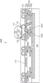
A MIM capacitor 113 is formed in the passivation layer 111. Fig. 1B shows an enlarged view of region 102 in fig. 1A to show details of MIM capacitor 113. As shown in fig. 1B, each MIM capacitor 113 includes two metal layers 113M (e.g., copper layers) and a dielectric layer 113I (e.g., a high-k dielectric layer) located between the metal layers 113M. Each layer (e.g., 113M, 113I, and 113M) of the MIM capacitor 113 is formed in a respective passivation layer (e.g., 111B, 111C, or 111D). As an example, the upper and lower metal layers 113M and 113M of the MIM capacitor 113 can be connected to the overlying and underlying vias 119V and 108, respectively, wherein the overlying and underlying vias 119V and 108 are formed in passivation layers 111E and 111A, respectively. As another example, the upper metal layer 113M and the lower metal layer 113M of the MIM capacitor 113 may be connected to the first overlying via 119V1 and the second overlying via 119V2, respectively. In the example of fig. 1B, second overlying via 119V2 extends through passivation layer 111D and dielectric layer 113I to connect with lower metal layer 113M. Note that second overlying via 119V2 extends through an opening in upper metal layer 113M of the MIM capacitor and is thus separated from (e.g., does not contact) upper metal layer 113M of the MIM capacitor by portions of passivation layer 111D.
Referring back to fig. 1A, the lower metal layer of MIM capacitor 113 may be electrically coupled to the conductive features of interconnect structure 106, for example, by vias extending from the lower metal layer of MIM capacitor 113 to the conductive features of interconnect structure 106. Further, multiple MIM capacitors 113 may be electrically coupled in parallel to provide a large capacitance value. For example, the upper metal layers of the MIM capacitor 113 may be electrically coupled together, and the lower metal layers of the MIM capacitor 113 may be electrically coupled together. In some embodiments, the MIM capacitor 113 is omitted.
Referring next to fig. 2, an opening 112 is formed in the passivation layer 111. Some of the openings 112 extend through the passivation layer 111 to expose conductive features of the interconnect structure 106. In some embodiments, some of the openings 112 extend partially through the passivation layer 111 to expose an upper metal layer of the MIM capacitor 113. The openings 112 may be formed in one or more etching processes (e.g., an anisotropic etching process).
After forming the opening 112, a barrier layer 115 is conformally formed over the upper surface of the passivation layer 111 and along the sidewalls and bottom of the opening 112. The barrier layer 115 may have a multi-layer structure, and may include a diffusion barrier layer (e.g., a TiN layer) and a seed layer (e.g., a copper seed layer) formed over the diffusion barrier layer. The barrier layer 115 may be formed using any suitable formation method(s), such as CVD, PVD, ALD, combinations thereof, and the like.
Next, in fig. 3, a photoresist layer 137 is formed over the barrier layer 115. The photoresist layer 137 is patterned (e.g., using photolithographic techniques) to form openings 138 at locations where conductive pads 119 (see fig. 4) are to be formed. The opening 138 exposes a seed layer, such as the barrier layer 115. After forming the opening 138, a descum (descum) process 110 is performed to remove residues left by the patterning process of the photoresist layer 137. As an example, the deslagging process 110 may be a plasma process performed using a process gas containing oxygen.
Next, in fig. 4, conductive pads 119 (e.g., 119A and 119B) are formed in openings 138 over barrier layer 115. The conductive pad 119 may include a conductive material such as copper or a copper alloy (e.g., a copper-silver alloy, a copper-cobalt alloy, etc.) and may be formed using a suitable formation method (e.g., electroplating, electroless plating, etc.). After the conductive pad 119 is formed, the photoresist layer 137 is removed by a suitable removal process (e.g., ashing). Next, an etching process is performed to remove a portion of the barrier layer 115 on which the conductive pad 119 is not formed. As shown in fig. 4, portions of the conductive material fill the openings 112 in the passivation layer 111 (see fig. 3) to form vias 119V that electrically couple the conductive pads 119 to the MIM capacitor 113 and/or conductive features of the underlying interconnect structure 106. Note that in the discussion herein, the barrier layer 115 in the opening 112 is considered to be part of the via 119V, and the barrier layer 115 over the upper surface of the passivation layer 111 is considered to be part of the conductive pad 119. Although not shown in fig. 4, a conductive line (e.g., a copper line) may also be formed on the upper surface of the passivation layer 111 (see, e.g., 118 in fig. 12) during the same processing step as the formation of the conductive pad 119. Conductive pads 119 and conductive lines may be collectively referred to as a redistribution layer (RDL), and vias 119V may be referred to as RDL vias. As an example, the shape of the cross-section of the conductive pad 119 may be dome-shaped (e.g., having a curved upper surface), concave, polygonal, or rectangular (or square). By way of example, the area of RDL via 119V may be about 0.9x0.9 μm2And about 3.5x3.5 μm2In the meantime, the method is described.
Note that in fig. 4, some conductive pads 119 (e.g., 119A) are larger (e.g., have a larger width measured between opposing sidewalls) than other conductive pads 119 (e.g., 119B). In some embodiments, controlled collapse chip connection bumps (C4 bumps) are formed on the larger conductive pads 119A and micro bumps (μ bumps) are formed on the smaller conductive pads 119B. As will be readily appreciated by the skilled artisan, the number of conductive pads 119 may be any suitable number and may be arranged in any order. Further, although one RDL via 119V is shown in fig. 4 under each conductive pad 119, the number of RDL vias 119V under each conductive pad 119 may be any suitable number, such as one, two, three, or more. Further, RDL via 119V under each conductive pad 119 may be centered with respect to conductive pad 119, or may be off-center with respect to conductive pad 119.
Next, in fig. 5, a passivation layer 121 is conformally formed over conductive pad 119 and over passivation layer 111. In some embodiments, passivation layer 121 has a multi-layer structure and includes an oxide layer (e.g., silicon oxide) and a nitride layer (e.g., silicon nitride) over the oxide layer. In other embodiments, passivation layer 121 has a single layer structure, for example, having a single nitride layer. Passivation layer 121 may be formed using, for example, CVD, PVD, ALD, combinations thereof, and the like.
Next, in fig. 6, a photoresist layer 135 is formed over the passivation layer 121 by, for example, spin coating. The photoresist layer 135 is then patterned, for example by photolithographic techniques, to form openings 136 at the locations where conductive bumps are to be formed. Next, an etching process is performed to remove the portion of the passivation layer 121 exposed by the opening 136. In some embodiments, the etching process is performed using a process including CF4、CHF3、N2And Ar (e.g., plasma etch process). Other process gases may also be used, for example, O may be used2Substitute for CF4. After the etching process, the conductive pad 119 is exposed. Next, the photoresist layer 135 is removed by a suitable removal process (e.g., ashing). Note that for simplicity, only one opening 136 is shown in fig. 6 over the larger conductive pad 119A used to form the conductive bump 125 (see fig. 8A), and no openings are formed over the other conductive pads (e.g., 119B). Of course, this is only one non-limiting example. As will be readily appreciated by those skilled in the art,the same or similar processing steps may be performed to form conductive bumps over other conductive pads (e.g., 119B).
Next, in fig. 7, a dielectric layer 131 is formed over passivation layer 121, over conductive pad 119, and over passivation layer 111. An opening 132 is formed in dielectric layer 131 to expose the underlying conductive pad 119. The dielectric layer 131 may be formed of, for example, a polymer, Polyimide (PI), benzocyclobutene (BCB), an oxide (e.g., silicon oxide), or a nitride (e.g., silicon nitride). As a non-limiting example, dielectric layer 131 is shown as a single layer in fig. 7. The dielectric layer 131 may have a multi-layered structure including a plurality of sub-layers formed of different dielectric materials.
In some embodiments, dielectric layer 131 is a photosensitive material, such as a photopolymer material, and opening 132 is formed using photolithographic techniques. For example, the photosensitive material may be exposed to a patterned energy source (e.g., light) through, for example, a reticle (reticle). The impact of the energy causes a chemical reaction in those portions of the photosensitive material that are impacted by the patterned energy source, thereby altering the physical properties of the exposed portions of the photosensitive material such that the physical properties of the exposed portions of the photosensitive material are different from the physical properties of the unexposed portions of the photosensitive material. The photosensitive material can then be developed with a developer to remove either the exposed portions of the photosensitive material or the unexposed portions of the photosensitive material, depending on, for example, whether a negative or positive photosensitive material is used. The remaining portions of the photosensitive material may be cured to form the patterned dielectric layer 131. As a non-limiting example, in fig. 7, the top corner of dielectric layer 131 at opening 132 is shown as sharp (e.g., comprising two intersecting lines). The top corners of the dielectric layer 131 at the openings 132 may be rounded, for example.
In fig. 7, a first distance between opposing sidewalls 131S of dielectric layer 131 exposed by opening 132 is less than a second distance between opposing sidewalls 121S of passivation layer 121 exposed by opening 136 in fig. 6. In other words, opening 132 in dielectric layer 131 is narrower than opening 136 in passivation layer 121 such that upper surface 121U and sidewalls 121S of passivation layer 121 are completely covered by dielectric layer 131. Opening 132 in fig. 7 is referred to as a pull-in opening because dielectric layer 131 is pulled in from sidewalls 121S of passivation layer 121. As a non-limiting example, the sidewalls 131S of the dielectric layer 131 are shown in fig. 7 as having a linear profile (e.g., a sloped line, or a flat sidewall that is sloped with respect to the major upper surface of the substrate 101). The sidewall 131S may be straight (e.g., perpendicular to the major upper surface of the substrate 101) or curved. The width of the opening 132 (e.g., the distance measured between the opposing sidewalls 131S) may be constant, or may vary continuously (e.g., gradually, without a step change) along the depth direction of the opening 132.
The pull-in opening 132 improves device reliability and production yield as compared to a pull-out opening (pulled-out opening). In the pull-out opening, the sidewalls 131S of the dielectric layer 131 are pulled out of the opening 132 to the position shown by the dashed lines 130 in fig. 7. In other words, if opening 132 were formed as a pull-out opening, the width of opening 132 would be greater than the width of opening 136 in FIG. 6. When the pull-out opening is formed, the interface between dielectric layer 131 and passivation layer 121 has much higher mechanical stress at the region near dashed line 130 (e.g., between the portion of dielectric layer 131 over conductive pad 119 and the portion of passivation layer 121 over conductive pad 119) than other regions of the device. The increased stress may cause delamination of the material layers in the high stress regions, resulting in device failure and reduced production yield. Furthermore, in subsequent processes of forming the seed layer 126 (see fig. 8A) for forming the conductive bump 125, the pull-out opening may be more challenging for forming the conformal, continuous seed layer 126 (the seed layer 126 lines the sidewalls and bottom of the pull-out opening) because the pull-out opening has a more stepped shape to be covered by the conformal seed layer 126. This is known as the bump seed layer step coverage problem. Bump seed layer step coverage issues may result in discontinuities (e.g., holes) in the seed layer 126, which in turn may result in defects in the conductive bumps 125 formed thereon. The present disclosure avoids or reduces the above-described problems by forming pull-in openings for forming the conductive bumps 125, thereby improving device reliability and production yield. Note that in addition to the pull-in opening, the aligned opening (see, e.g., aligned opening 136 in fig. 10 and the discussion thereof) provides the same or similar advantages as the pull-in opening. In some embodiments, the openings (e.g., 132, 136) used to form the conductive bumps 125 are pull-in openings and/or alignment openings, and no pull-out openings are formed to form the conductive bumps 125.
Next, in fig. 8A, a conductive bump 125 is formed on the conductive pad 119, and a solder region 129 is formed on the conductive bump 125. The width of the conductive bump 125 may be between about 5 μm and about 90 μm. The conductive bumps 125 may be μ bumps or C4 bumps. For example, μ bumps having a width (e.g., a width measured between opposing sidewalls) of between about 5 μm and about 30 μm, for example, can be formed over conductive pads 119B, and C4 bumps having a width of between about 32 μm and about 90 μm can be formed over conductive pads 119A. In an example embodiment, each of the μ bump and the C4 bump is formed in a pull-in opening 132 (see fig. 7) formed over a respective conductive pad 119.
The conductive bump 125 may be formed by: forming a seed layer 126 over the dielectric layer 131 and along the sidewalls and bottom of the opening 132; forming a patterned photoresist layer over the seed layer 126, wherein openings of the patterned photoresist layer are formed at locations where the conductive bumps 125 are to be formed; forming (e.g., electroplating) a conductive material (e.g., copper) over the seed layer 126 in the opening; removing the patterned photoresist layer; and removing a portion of the seed layer 126 on which the conductive bump 125 is not formed. Note that some portion of the conductive material fills opening 132 to form bump via 125V, which bump via 125V electrically couples conductive bump 125 to underlying conductive pad 119. Note that in the discussion herein, the seed layer 126 in the opening 132 (see fig. 7) is considered to be part of the bump via 125V, and the seed layer 126 above the upper surface of the dielectric layer 131 is considered to be part of the conductive bump 125. By way of example, fig. 8A illustrates an interface between the conductive material (e.g., copper) of the conductive bump 125 and the seed layer 126. In some embodiments, the conductive material of the conductive bump 125 and the seed layer 126 are formed of the same material, and thus there may be no interface between them.
In fig. 8A, the number of bump vias 125V under (e.g., directly under) each conductive bump 125 is one. Of course, this is only a non-limiting example. The number of bump vias 125V under each conductive bump 125 may be any suitable number, such as one, two, three, or more. Further, the one or more bump vias 125V under each conductive bump 125 may be centered with respect to the conductive bump 125, or may be off-center with respect to the conductive bump 125.
In fig. 8A, the sidewalls of the bump via 125V contact (e.g., physically contact) the sidewalls of the dielectric layer 131 and extend along the sidewalls of the dielectric layer 131. The width of the bump via 125V may be constant (e.g., having sidewalls perpendicular to the major upper surface of the substrate 101), or may vary continuously (e.g., gradually without a step change, or without a discontinuous change) as the bump via 125V extends toward the substrate 101. In the example of fig. 8A, the sidewalls of the bump via 125V have a linear profile (e.g., a slanted straight line), and the width of the bump via 125V continuously decreases as the bump via 125V extends toward the substrate 101. The sidewalls of the bump via 125V may have a curved profile (e.g., a curve), such as when the sidewalls 131S (see fig. 7) of the dielectric layer 131 exposed by the opening 132 have a curved profile. Note that there is a gap between the sidewalls of bump via 125V and the corresponding sidewalls of passivation layer 121, and dielectric layer 131 fills the gap and contacts the upper surface of conductive pad 119A. In other words, the bump via 125V is spaced apart (e.g., separated) from the passivation layer 121 by a portion of the dielectric layer 131 laterally disposed between the bump via 125V and the passivation layer 121.
In the example of fig. 8A, the thickness a of the portion of dielectric layer 131 disposed over passivation layer 121 on conductive pad 119 is between about 1 μm and about 20 μm. The spacing S between adjacent smaller conductive pads 119B (e.g., having μ bumps formed thereon) is greater than about 1.5 μm, and the spacing S between adjacent larger conductive pads 119A (e.g., having C4 bumps formed thereon) is greater than about 4 μm. Fig. 8A also shows a thickness T of a sidewall portion of passivation layer 121 (e.g., along a sidewall of conductive pad 119, or along a portion of a sidewall of conductive line 118 in fig. 16A), and a thickness G of an upper portion of passivation layer 121 (e.g., along an upper surface of conductive pad 119, or along a portion of an upper surface of conductive line 118), wherein thickness G is between about 0.5 μm and about 5 μm, and wherein a ratio between T and G (e.g., T/G), referred to as a step coverage of passivation layer 121, is between about 20% and about 95%. In some embodiments, the pitch P between adjacent conductive bumps 125 is between about 10 μm and about 140 μm.
Fig. 8B illustrates an enlarged view of the portion of the semiconductor device 100 of fig. 8A that includes the conductive bump 125. The dimensions of the conductive bump 125 and its surrounding structure are discussed below.
As shown in fig. 8B, the width W of the conductive bump 125 (e.g., a C4 bump or μ bump) is between about 5 μm and about 90 μm. The width B at the top of the opening 132 in the dielectric layer 131 is between about 5 μm and about 22 μm for μ bumps and between about 5 μm and about 78 μm for C4 bumps. Note that width W in fig. 8B is measured along the horizontal direction of fig. 8B, and opening 132 has another width W2 measured along a direction perpendicular to the cross-section of fig. 8B (e.g., out of the page and along the longitudinal axis of conductive line 118 in fig. 16B), where width W2 is between about 5 μm and about 36 μm for μ bumps, and between about 20 μm and about 40 μm for C4 bumps. The width E at the bottom of the opening 132 in the dielectric layer 131 is between about 5 μm and about 22 μm for μ bumps and between about 5 μm and about 78 μm for C4 bumps. The height D of the bump via 125V is greater than the thickness a of the dielectric layer 131 (see fig. 8A) and greater than the thickness G of the passivation layer 121 (see fig. 8A).
Still referring to fig. 8B, the width L of the conductive pad 119 is between about 5 μm and about 45 μm if the conductive pad 119 is a larger conductive pad 119A (e.g., having a C4 bump formed thereon), or between about 1.5 μm and about 10 μm if the conductive pad is a smaller conductive pad 119B (e.g., having a μ bump formed thereon). The ratio between the width L of the conductive pad 119 and the pitch S (see fig. 8A) is equal to or greater than one. The height J of the conductive pad 119 (or conductive line 118 in fig. 16A) is between about 2 μm and about 6 μm. Fig. 8B also shows an angle F ' between the sidewalls of dielectric layer 131 and the upper surface of conductive pad 119, and an angle F between the sidewalls of passivation layer 121 and the upper surface of conductive pad 119, where F may be between 10 degrees and 90 degrees (e.g., 10 ° < F <90 °), and F ' may be between 10 degrees and 90 degrees (e.g., 10 ° < F ' <90 °). If the opening (e.g., 136 in fig. 10) in which the conductive bump 125 is formed is an aligned opening, then the respective F and F' are equal. Otherwise, F may be different from F'.
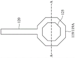
Fig. 8C shows a plan view of the semiconductor device 100 of fig. 8B, and fig. 8B corresponds to a sectional view along the section a-a of fig. 8C. Note that for simplicity, not all features are shown in fig. 8C. As a non-limiting example, conductive pad 119 in fig. 8C is shown as having an octagonal shape. Other shapes (e.g., circular, oval, rectangular, other polygonal, etc.) are also possible and are fully intended to be included within the scope of the present disclosure. In the example of fig. 8C, conductive bump 125 is shown as having a similar geometry as conductive pad 119. In other embodiments, the conductive bump 125 and the conductive pad 119 have different shapes (e.g., non-geometrically similar shapes). Fig. 8C also shows conductive line 120 connected to conductive pad 119. Conductive lines 120 extend along the upper surface of dielectric layer 131 and, together with conductive pads 119, form part of a redistribution layer.
Fig. 9-11 illustrate cross-sectional views of a semiconductor device 100B at various stages of fabrication, in accordance with another embodiment. Semiconductor device 100B is similar to semiconductor device 100 of fig. 8A, but has aligned openings 136 (see fig. 10) for exposing conductive pads 119A and for forming conductive bumps 125. The process of fig. 9 follows the process of fig. 1A, 1B, and 2-5. In other words, fig. 1A, 1B, 2-5, and 9-11 illustrate processing steps for forming the semiconductor device 100B.
In fig. 9, after forming passivation layer 121, dielectric layer 131 is formed over passivation layer 121, and opening 132 is formed in dielectric layer 131 to expose passivation layer 121. The formation of dielectric layer 131 and the formation of opening 132 may use the same or similar processes as discussed above with reference to fig. 7, and therefore, the details are not repeated. Note that up to this stage of processing, no openings are formed in passivation layer 121 over conductive pad 119. Thus, the upper surface of the conductive pad 119 is covered by the passivation layer 121.
Next, in fig. 10, a patterned photoresist layer 133 is formed over the dielectric layer 131. The openings 136 of the patterned photoresist layer 133 overlie the respective openings 132 of the dielectric layer 131 (see fig. 9). In some embodiments, the width of opening 136 measured at the upper surface of dielectric layer 131 is the same as the width of opening 132 measured at the upper surface of dielectric layer 131. In other embodiments, the width of opening 136 measured at the upper surface of dielectric layer 131 is greater than the width of opening 132 measured at the upper surface of dielectric layer 131. Next, the patterned photoresist layer 133 serves as an etch mask for a subsequent etching process, which may be the same as or similar to the etching process in fig. 6 exposing the conductive pad 119A. As shown in fig. 10, after the etching process, opening 136 extends down through passivation layer 121 and exposes conductive pad 119A.
Still referring to fig. 10, the opening 136 is formed as an aligned opening. For each aligned opening 136, sidewalls 131S of the dielectric layer 131 exposed by the opening 136 and corresponding sidewalls 121S of the passivation layer 121 exposed by the opening 136 are aligned along the same line (e.g., a straight line perpendicular to the major upper surface of the substrate 101, or an inclined line with respect to the major upper surface of the substrate 101, or a curved line). Stated differently, the distance between opposing sidewalls of the opening 136 varies continuously (e.g., gradually without a step change) along the depth direction of the opening 136. After the aligned opening 136 is formed, the photoresist layer 133 is removed, for example, by an ashing process.
Next, in fig. 11, after the same or similar process as fig. 8A, a conductive bump 125 is formed over the conductive pad 119, and details are not repeated. In the example of fig. 11, an upper sidewall (e.g., an upper portion of the sidewall) of the bump via 125V contacts the sidewall 131S of the dielectric layer 131 and extends along the sidewall 131S of the dielectric layer 131, and a lower sidewall (e.g., a lower portion of the sidewall) of the bump via 125V contacts the sidewall 121S of the passivation layer 121 and extends along the sidewall 121S of the passivation layer 121. In some embodiments, the width of bump via 125V (e.g., the width measured between opposing sidewalls of bump via 125V) is constant (e.g., with straight sidewalls) or varies continuously (e.g., gradually without a step change) as bump via 125V extends toward substrate 101.
Fig. 12-15, 16A, and 16B illustrate cross-sectional views of a semiconductor device 100C at various stages of fabrication according to yet another embodiment. Semiconductor device 100C is similar to semiconductor device 100B of fig. 11, except that conductive bump 125 is formed over conductive line 118 instead of over conductive pad 119. The process of fig. 12 follows the process of fig. 1A, 1B, and 2. In other words, fig. 1A, 1B, 2, 12-15, 16A, and 16B illustrate processing steps for forming the semiconductor device 100C. Note that although the semiconductor devices 100, 100B, and 100C are described as different embodiments, any combination of the semiconductor devices 100, 100B, and 100C (e.g., 100 and 100C, or 100B and 100C) may be formed on the same substrate 101, e.g., in different regions of the same substrate 101.
In fig. 12, a plurality of conductive lines 118 are formed over the passivation layer 111 using a process similar to that shown in fig. 3. In some embodiments, to form the conductive lines 118, a patterned photoresist layer 137 (see, e.g., fig. 3) is formed over the barrier layer 115, wherein the locations of the patterns (e.g., openings) of the patterned photoresist layer 137 correspond to the locations of the subsequently formed conductive lines 118. Next, the deslagging process 110 is performed. Next, a conductive material (e.g., copper) is formed in the pattern of patterned photoresist layer 137 over barrier layer 115. Next, the patterned photoresist layer 137 is removed, and an etching process is performed to remove portions of the barrier layer 115 on which the conductive material is not formed.
Next, in fig. 13, a passivation layer 121 is conformally formed over conductive line 118 and over passivation layer 111. The formation of passivation layer 121 is the same or similar to the process discussed above with reference to fig. 5 and therefore details are not repeated.
Next, in fig. 14, a dielectric layer 131 is formed over the passivation layer 121, and an opening 132 is formed in the dielectric layer 131 to expose the passivation layer 121 disposed over the upper surface of the conductive line 118. The formation of the dielectric layer 131 and the opening 132 is the same or similar to the process discussed above with reference to fig. 7 and therefore the details are not repeated. Note that up to this stage of processing, no openings are formed in passivation layer 121 that expose conductive lines 118.
Next, in fig. 15, a photoresist layer 133 is formed over the dielectric layer 131, and an opening 136 is formed in the photoresist layer 133 overlying the opening 132 (see fig. 14). Next, an etching process (e.g., an anisotropic etching process) is performed using the patterned photoresist layer 133 as an etch mask to extend the opening 136 downward such that the opening 136 extends through the passivation layer 121 to expose the conductive line 118. The etching process may be the same as or similar to the etching process discussed above with reference to fig. 6, and therefore, details are not repeated. Note that opening 136 is an aligned opening due to, for example, an anisotropic etch process used to form opening 136.
Next, in fig. 16A, after the same or similar process as fig. 8A, a conductive bump 125 is formed over the conductive line 118, and details are not repeated. In the example of fig. 16A, two bump vias 125V are formed under the conductive bump 125 and electrically couple the conductive bump 125 to the two underlying conductive lines 118. In other words, each bump via 125V extends into the dielectric layer 131, through the passivation layer 121, and contacts (e.g., physically contacts) the underlying conductive line 118, thereby electrically coupling the conductive bump 125 with the underlying conductive line 118. The number of bump vias 125V under each conductive bump 125 and the number of conductive lines 118 electrically coupled to an overlying conductive bump 125 shown in fig. 16A are merely non-limiting examples, and any suitable number of bump vias 125V and conductive lines 118 may be formed under each conductive bump 125.
As shown in fig. 16A, upper sidewalls (e.g., upper portions of the sidewalls) of the bump via 125V contact the sidewalls 131S of the dielectric layer 131 and extend along the sidewalls 131S of the dielectric layer 131, and lower sidewalls (e.g., lower portions of the sidewalls) of the bump via 125V contact the sidewalls 121S of the passivation layer 121 and extend along the sidewalls 121S of the passivation layer 121. In some embodiments, the width of the bump via 125V (e.g., the width measured between opposing sidewalls of the bump via 125V) is constant (e.g., has straight sidewalls) or varies continuously (e.g., gradually without a step change) as the bump via 125V extends toward the substrate 101.
Fig. 16B shows a plan view of a part of the semiconductor device 100C of fig. 16A, and fig. 16A corresponds to a sectional view along a section B-B of fig. 16B. Note that not all features are shown in fig. 16B for simplicity. As a non-limiting example, the conductive bump 128 in fig. 16B is shown as having an octagonal shape. Other shapes (e.g., circular, elliptical, rectangular, other polygonal, etc.) are also possible and are fully intended to be included within the scope of the present disclosure.
Variations or modifications to the disclosed embodiments are possible and are fully intended to be included within the scope of the present disclosure. For example, although different embodiments 100, 100B, and 100C are described as different semiconductor devices, different structures/shapes of the conductive bumps 125 disclosed in embodiments 100, 100B, and 100C may be formed in different regions of the same semiconductor device. In other words, the semiconductor device may have different conductive bump structures disclosed in fig. 8A, 11, and 16A formed in different regions of the same semiconductor device.
Embodiments of the present disclosure achieve some advantageous features. For example, by forming a pull-in opening (see, e.g., 132 in fig. 7) or an aligned opening (see, e.g., 136 in fig. 10), adhesion between the dielectric layer 131 and the passivation layer 121 is improved, and mechanical stress in the device near the interface between the dielectric layer 131 and the passivation layer 121 (e.g., at the lower corner of the dielectric layer 131 facing the opening) is reduced. The improved adhesion and reduced stress help reduce or prevent delamination at the interface between dielectric layer 131 and passivation layer 121, thereby improving device performance, device reliability, and production yield. As another example, the formation of dielectric layer 131 eliminates some of the difficulties associated with forming conductive bumps 125 and improves device reliability and manufacturing yield. Recall that to form the conductive bumps 125, the seed layer 126 is first formed, and then a conductive material is formed (e.g., plated) over the seed layer 126. Without the dielectric layer 131, the seed layer 126 would have to be formed conformally over the conductive pads 119 and/or over the conductive lines 118. In advanced semiconductor manufacturing, small gaps between conductive pads 119 or between conductive lines 118 may have a high aspect ratio, and it may be difficult to form seed layer 126 in these small gaps, which may result in improper formation of conductive bumps 125. In addition, after the conductive bump 125 is formed, a portion of the seed layer 126 on which the conductive bump 125 is not formed needs to be removed. If these portions of the seed layer 126 are located in small gaps, it may be difficult to remove the seed layer 126, which may result in electrical shorts between the conductive bumps 125. In contrast, in the case where the dielectric layer 131 is formed, the seed layer 126 is formed over the dielectric layer 131 and in the openings 132 or 136, these openings 132/136 have a smaller aspect ratio, and therefore the seed layer 126 can be easily formed in the openings and easily removed therefrom, thereby avoiding the problems discussed above.
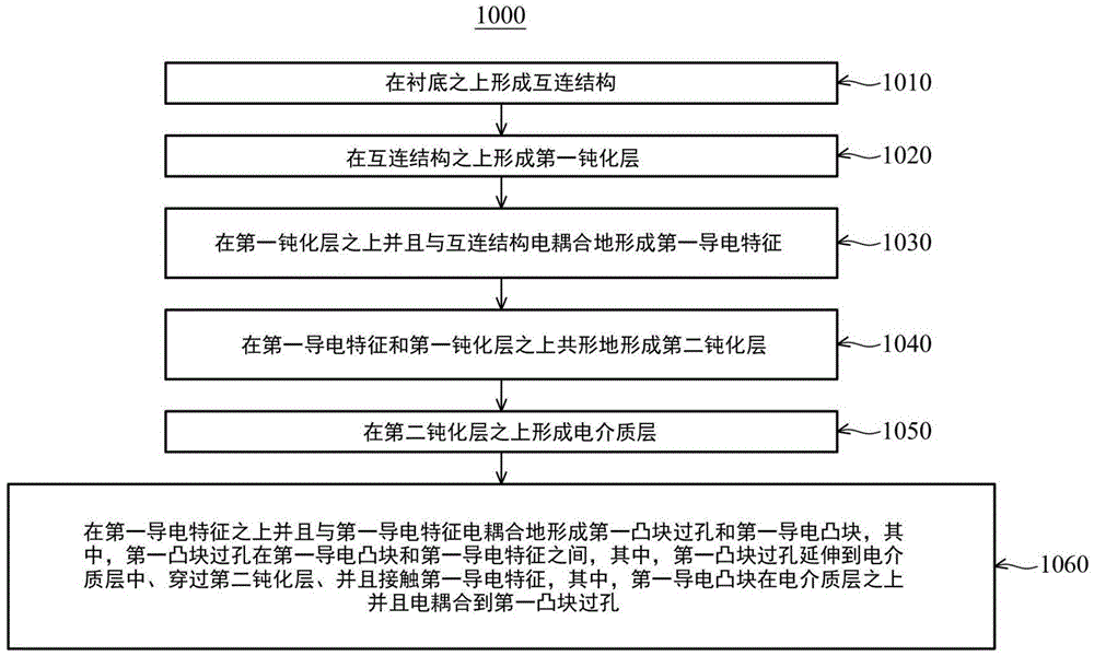
Figure 17 illustrates a flow diagram of a method 1000 of fabricating a semiconductor structure, according to some embodiments. It should be understood that the embodiment method shown in FIG. 17 is only one example of many possible embodiment methods. One of ordinary skill in the art would recognize many variations, alternatives, and modifications. For example, various steps as shown in fig. 17 may be added, removed, replaced, rearranged, or repeated.
Referring to fig. 17, at block 1010, an interconnect structure is formed over a substrate. At block 1020, a first passivation layer is formed over the interconnect structure. At block 1030, a first conductive feature is formed over the first passivation layer and electrically coupled with the interconnect structure. At block 1040, a second passivation layer is conformally formed over the first conductive feature and the first passivation layer. At block 1050, a dielectric layer is formed over the second passivation layer. At block 1060, a first bump via and a first conductive bump are formed over and electrically coupled with the first conductive feature, wherein the first bump via is between the first conductive bump and the first conductive feature, wherein the first bump via extends into the dielectric layer, through the second passivation layer, and contacts the first conductive feature, wherein the first conductive bump is over the dielectric layer and electrically coupled to the first bump via.
According to an embodiment of the present disclosure, a method of forming a semiconductor device includes: forming an interconnect structure over a substrate; forming a first passivation layer over the interconnect structure; forming a first conductive feature over the first passivation layer and electrically coupled with the interconnect structure; conformally forming a second passivation layer over the first conductive feature and the first passivation layer; forming a dielectric layer over the second passivation layer; and forming a first bump via and a first conductive bump over and electrically coupled with the first conductive feature, wherein the first bump via is between the first conductive bump and the first conductive feature, wherein the first bump via extends into the dielectric layer, through the second passivation layer, and contacts the first conductive feature, wherein the first conductive bump is over the dielectric layer and electrically coupled to the first bump via.
According to one embodiment of the present disclosure, a method of forming a semiconductor device includes: forming a first passivation layer over the interconnect structure, wherein the interconnect structure is over and electrically coupled to an electronic component formed in the substrate; forming a conductive feature over the first passivation layer, wherein the conductive feature is electrically coupled to the interconnect structure; forming a second passivation layer over the conductive feature and the first passivation layer, wherein the second passivation layer is conformal and extends along an outer surface of the conductive feature; forming a dielectric layer over the second passivation layer, wherein an upper surface of the dielectric layer remote from the substrate extends further from the substrate than an upper surface of the conductive feature remote from the substrate; forming a bump via extending from an upper surface of the dielectric layer to an upper surface of the conductive feature, wherein a width of the bump via continuously varies as the bump via extends toward the conductive feature; and forming a conductive bump on the bump via.
According to an embodiment of the present disclosure, a semiconductor device includes: a substrate including a device region; an interconnect structure over the substrate and electrically coupled to the device region; a first passivation layer over the interconnect structure; a conductive feature over the first passivation layer and electrically coupled to the interconnect structure; a second passivation layer over the conductive feature and the first passivation layer, wherein the second passivation layer is conformal and extends along an outer surface of the conductive feature; a dielectric layer over the second passivation layer, wherein the dielectric layer extends further from the substrate than the conductive features; a bump via in the dielectric layer, wherein the bump via extends from an upper surface of the dielectric layer away from the substrate to the conductive feature, wherein a width of the bump via continuously varies as the bump via extends toward the conductive feature; and a conductive bump on the bump via.
Example 1 is a method of forming a semiconductor device, the method comprising: forming an interconnect structure over a substrate; forming a first passivation layer over the interconnect structure; forming a first conductive feature over the first passivation layer and electrically coupled with the interconnect structure; conformally forming a second passivation layer over the first conductive feature and the first passivation layer; forming a dielectric layer over the second passivation layer; and forming a first bump via and a first conductive bump over and electrically coupled to the first conductive feature, wherein the first bump via is between the first conductive bump and the first conductive feature, wherein the first bump via extends into the dielectric layer, through the second passivation layer, and contacts the first conductive feature, wherein the first conductive bump is over the dielectric layer and electrically coupled to the first bump via.
Example 2 is the method of example 1, wherein the dielectric layer surrounds the first conductive feature, and an upper surface of the dielectric layer remote from the substrate extends further from the substrate than the first conductive feature.
Example 3 is the method of example 1, wherein forming the first bump via and the first conductive bump comprises: forming a first opening in the second passivation layer to expose an upper surface of the first conductive feature after forming the second passivation layer and before forming the dielectric layer; forming a second opening in the dielectric layer to expose an upper surface of the first conductive feature after forming the dielectric layer, wherein a sidewall of the second passivation layer facing the second opening is covered by the dielectric layer after forming the second opening; and forming a conductive material filling the second opening and extending over an upper surface of the dielectric layer remote from the substrate.
Example 4 is the method of example 3, wherein a first portion of the conductive material in the second opening forms the first bump via and a second portion of the conductive material above an upper surface of the dielectric layer forms the first conductive bump.
Example 5 is the method of example 3, wherein a second width of the second opening measured between opposing sidewalls of the second opening is less than a first width of the first opening measured between opposing sidewalls of the first opening.
Example 6 is the method of example 5, wherein a second width of the second opening varies continuously along a depth direction of the second opening.
Example 7 is the method of example 1, wherein forming the first bump via and the first conductive bump comprises: after forming the dielectric layer, forming a first opening in the dielectric layer, the first opening extending into the dielectric layer to expose an upper surface of the second passivation layer distal from the substrate, wherein the second passivation layer exposed at the bottom of the first opening extends along and covers an upper surface of the first conductive feature; after forming the first opening, forming a patterned mask layer over the dielectric layer, wherein a second opening in the patterned mask layer overlies the first opening; and performing an anisotropic etch process using the patterned mask layer as an etch mask, wherein the anisotropic etch process extends the second opening through the second passivation layer to expose an upper surface of the first conductive feature.
Example 8 is the method of example 7, wherein, after the anisotropic etching process, sidewalls of the dielectric layer facing the second opening are aligned along a same line with respective sidewalls of the second passivation layer facing the second opening.
Example 9 is the method of example 7, further comprising: after the anisotropic etching process, forming a conductive material over an upper surface of the first conductive feature, wherein a first portion of the conductive material in the dielectric layer forms the first bump via and a second portion of the conductive material over an upper surface of the dielectric layer forms the first conductive bump.
Example 10 is the method of example 7, wherein the first conductive feature is a first conductive line.
Example 11 is the method of example 10, wherein the method further comprises: forming a second conductive line over the first passivation layer adjacent to the first conductive line, wherein the second passivation layer is conformally formed over the second conductive line; and forming a second bump via between the first conductive bump and the second conductive line, wherein the second bump via extends into the dielectric layer, through the second passivation layer, and contacts the second conductive line, wherein the first conductive bump is electrically coupled to the first bump via and the second bump via.
Example 12 is the method of example 1, further comprising: forming a Metal Insulator Metal (MIM) capacitor in the first passivation layer, wherein the first conductive feature is formed to be electrically coupled to the MIM capacitor.
Example 13 is a method of forming a semiconductor device, the method comprising: forming a first passivation layer over an interconnect structure, wherein the interconnect structure is over and electrically coupled to an electronic component formed in a substrate; forming a conductive feature over the first passivation layer, wherein the conductive feature is electrically coupled to the interconnect structure; forming a second passivation layer over the conductive feature and the first passivation layer, wherein the second passivation layer is conformal and extends along an outer surface of the conductive feature; forming a dielectric layer over the second passivation layer, wherein an upper surface of the dielectric layer distal from the substrate extends further from the substrate than an upper surface of the conductive feature distal from the substrate; forming a bump via extending from an upper surface of the dielectric layer to an upper surface of the conductive feature, wherein a width of the bump via varies continuously as the bump via extends toward the conductive feature; and forming a conductive bump on the bump via.
Example 14 is the method of example 13, wherein an upper sidewall of the bump via contacts and extends along a first sidewall of the dielectric layer facing the bump via, and a lower sidewall of the bump via contacts and extends along a second sidewall of the second passivation layer facing the bump via.
Example 15 is the method of example 14, wherein a first sidewall of the dielectric layer and a second sidewall of the second passivation layer are aligned along a same line.
Example 16 is the method of example 13, wherein the bump via is spaced apart from the second passivation layer by a portion of the dielectric layer laterally disposed between the bump via and the second passivation layer.
Example 17 is the method of example 13, further comprising: forming a Metal Insulator Metal (MIM) capacitor in the first passivation layer, wherein the conductive feature is formed to be electrically coupled to the MIM capacitor.
Example 18 is a semiconductor device, comprising: a substrate including a device region; an interconnect structure over the substrate and electrically coupled to the device region; a first passivation layer over the interconnect structure; a conductive feature over the first passivation layer and electrically coupled to the interconnect structure; a second passivation layer over the conductive feature and the first passivation layer, wherein the second passivation layer is conformal and extends along an outer surface of the conductive feature; a dielectric layer over the second passivation layer, wherein the dielectric layer extends further from the substrate than the conductive feature; a bump via in the dielectric layer, wherein the bump via extends from an upper surface of the dielectric layer remote from the substrate to the conductive feature, wherein a width of the bump via continuously varies as the bump via extends toward the conductive feature; and a conductive bump on the bump via.
Example 19 is the semiconductor device of example 18, wherein an upper sidewall of the bump via contacts and extends along a first sidewall of the dielectric layer facing the bump via, and a lower sidewall of the bump via contacts and extends along a second sidewall of the second passivation layer facing the bump via, wherein the first sidewall and the second sidewall are aligned along a same line.
Example 20 is the semiconductor device of example 18, wherein a portion of the dielectric layer is laterally disposed between the second passivation layer and the bump via such that the bump via is separated from the second passivation layer.
The foregoing has outlined features of several embodiments so that those skilled in the art may better understand the aspects of the present disclosure. Those skilled in the art should appreciate that they may readily use the present disclosure as a basis for designing or modifying other processes and structures for carrying out the same purposes and/or achieving the same advantages of the embodiments introduced herein. Those skilled in the art should also realize that such equivalent constructions do not depart from the spirit and scope of the present disclosure, and that they may make various changes, substitutions, and alterations herein without departing from the spirit and scope of the present disclosure.