CN114113116A - Accurate detection process method for micro-defects on surface of large-diameter element - Google Patents
Accurate detection process method for micro-defects on surface of large-diameter element Download PDFInfo
- Publication number
- CN114113116A CN114113116A CN202111429843.XA CN202111429843A CN114113116A CN 114113116 A CN114113116 A CN 114113116A CN 202111429843 A CN202111429843 A CN 202111429843A CN 114113116 A CN114113116 A CN 114113116A
- Authority
- CN
- China
- Prior art keywords
- defect
- sub
- image
- pixel
- scanning
- Prior art date
- Legal status (The legal status is an assumption and is not a legal conclusion. Google has not performed a legal analysis and makes no representation as to the accuracy of the status listed.)
- Granted
Links
Images


Classifications
-
- G—PHYSICS
- G01—MEASURING; TESTING
- G01N—INVESTIGATING OR ANALYSING MATERIALS BY DETERMINING THEIR CHEMICAL OR PHYSICAL PROPERTIES
- G01N21/00—Investigating or analysing materials by the use of optical means, i.e. using sub-millimetre waves, infrared, visible or ultraviolet light
- G01N21/84—Systems specially adapted for particular applications
- G01N21/88—Investigating the presence of flaws or contamination
-
- G—PHYSICS
- G01—MEASURING; TESTING
- G01N—INVESTIGATING OR ANALYSING MATERIALS BY DETERMINING THEIR CHEMICAL OR PHYSICAL PROPERTIES
- G01N21/00—Investigating or analysing materials by the use of optical means, i.e. using sub-millimetre waves, infrared, visible or ultraviolet light
- G01N21/01—Arrangements or apparatus for facilitating the optical investigation
- G01N2021/0106—General arrangement of respective parts
- G01N2021/0112—Apparatus in one mechanical, optical or electronic block
-
- G—PHYSICS
- G01—MEASURING; TESTING
- G01N—INVESTIGATING OR ANALYSING MATERIALS BY DETERMINING THEIR CHEMICAL OR PHYSICAL PROPERTIES
- G01N21/00—Investigating or analysing materials by the use of optical means, i.e. using sub-millimetre waves, infrared, visible or ultraviolet light
- G01N21/84—Systems specially adapted for particular applications
- G01N21/88—Investigating the presence of flaws or contamination
- G01N21/8851—Scan or image signal processing specially adapted therefor, e.g. for scan signal adjustment, for detecting different kinds of defects, for compensating for structures, markings, edges
- G01N2021/8887—Scan or image signal processing specially adapted therefor, e.g. for scan signal adjustment, for detecting different kinds of defects, for compensating for structures, markings, edges based on image processing techniques
-
- Y—GENERAL TAGGING OF NEW TECHNOLOGICAL DEVELOPMENTS; GENERAL TAGGING OF CROSS-SECTIONAL TECHNOLOGIES SPANNING OVER SEVERAL SECTIONS OF THE IPC; TECHNICAL SUBJECTS COVERED BY FORMER USPC CROSS-REFERENCE ART COLLECTIONS [XRACs] AND DIGESTS
- Y02—TECHNOLOGIES OR APPLICATIONS FOR MITIGATION OR ADAPTATION AGAINST CLIMATE CHANGE
- Y02P—CLIMATE CHANGE MITIGATION TECHNOLOGIES IN THE PRODUCTION OR PROCESSING OF GOODS
- Y02P90/00—Enabling technologies with a potential contribution to greenhouse gas [GHG] emissions mitigation
- Y02P90/30—Computing systems specially adapted for manufacturing
Abstract
A precise detection process method for micro-defects on the surface of a large-caliber element relates to the technical field of engineering optics and is used for solving the problem that the positioning precision for detecting the surface defects of the large-caliber element is low in the prior art. The technical points of the invention comprise: performing row-by-row and column-by-column mobile scanning on a preset scanning area on the surface of the element in a dark field environment, and acquiring a plurality of sub-aperture images of a plurality of preset photographing positions; and processing the plurality of sub-aperture images to obtain the positions and the actual sizes of a plurality of defect areas on the surface of the element. The invention realizes the collection of the dark field image on the surface of the large-caliber element by adopting a scanning photographing mode, and realizes the accurate extraction of the surface defect by image processing. The method is easy to realize automation, and can provide accurate position and size information for the positioning and repairing of subsequent defect points.
Description
Technical Field
The invention relates to the technical field of engineering optics, in particular to a process method for accurately detecting micro-defects on the surface of a large-caliber element.
Background
High power solid state laser devices use a large number of large aperture optical components that are used to perform the functions of laser transmission, amplification, frequency conversion, harmonic separation, and beam focusing. To achieve as high an output energy as possible, high power solid state laser devices are typically operated at a fluence close to the damage threshold of the optical element. And defects such as pits, microcracks and the like easily appear in the optical element in the processing process, and the generation and growth of the defects are further aggravated by high-power laser irradiation. Because of the high cost of the large-caliber optical element, CO is used in engineering for prolonging the service life of the element2The laser repairs the defect point, and the detection of obtaining the accurate position and size information of the defect point is the premise of realizing defect repair.
Common methods for detecting and positioning the micro-defects on the surface of the optical element include a visual detection method and a machine vision detection method. The visual inspection method is to irradiate the surface of the element with a strong light beam at a certain angle, and an operator observes the defect points presenting bright spots in the reflection direction or the transmission direction of the light beam. But the accurate position and size information of the defect can not be obtained by only visual identification, and the efficiency is low and the error rate is high. As technology has evolved, machine vision has been introduced in the detection of surface defects on optical elements. The method acquires the surface image of the optical element through the camera and processes the image to obtain the specific position and size of the surface defect, and is widely applied to optical element detection due to the advantages of high detection efficiency, easiness in realizing precision and automation of defect detection and the like. However, the existing method for detecting the large-aperture optical element mostly adopts a high-resolution camera single-frame shooting mode, has high cost, poor imaging effect and low resolution, and cannot meet the requirement of engineering on defect point positioning precision.
Disclosure of Invention
In view of the above problems, the present invention provides a precise detection process for surface micro-defects of a large-diameter element, so as to solve the problem of low positioning precision for surface defect detection of the large-diameter element in the prior art.
A process method for accurately detecting micro defects on the surface of a large-caliber element comprises the following steps:
firstly, performing row-by-row and column-by-column mobile scanning on a preset scanning area on the surface of an element, and acquiring a plurality of sub-aperture images of a plurality of preset photographing positions;
step two, processing the plurality of sub-aperture images to obtain the positions and actual sizes of a plurality of defect areas on the surface of the element; the method comprises the following specific steps:
secondly, performing image segmentation processing on each sub-aperture image to obtain a plurality of defect area images;
secondly, calculating the centers of the minimum circumscribed circles of all pixel points in the image enveloping the defect regions, and taking the centers as pixel coordinates corresponding to each defect region;
calculating according to the size of a preset scanning area, the number of sub-aperture images at a preset photographing position and the pixel coordinates to obtain the position of each defect area;
and step four, calculating the pixel size of the defect area through the calibrated physical size represented by one pixel to obtain the actual size of each defect area.
Further, in the first step, a dark field environment is formed by using the annular light source to irradiate the surface of the element at a low angle, and the sub-aperture image is scanned and acquired in the dark field environment.
Further, in the step one, in the process of moving and scanning row by row and column by column, a preset photographing position of each sub-aperture image under a machine tool coordinate system is set, and the preset photographing position of each sub-aperture image is as follows:

in the formula, xi,j、yi,j、zi,jRepresenting the photographing position of the jth row and ith column sub-aperture image in a machine tool coordinate system; x is the number ofo、yoX, Y axis coordinates in a machine coordinate system when the geometric center point of the element is at the center of the camera visual field; xs and Ys respectively represent scanning stepping values along the row direction and the column direction; sX、SYRespectively representing the distance between the scanning starting point and the geometric center point of the element in the direction of X, Y axes; z (.) represents the surface equation of the element with the geometric center point of the element as the origin of coordinates; z is a radical ofoAnd the Z-axis coordinate of the geometric center point of the element in the machine tool coordinate system when the camera is in clear focus is represented.
Further, the position of each defect area in the second step and the third step is calculated according to the following formula:

wherein, (x, y, z) represents the position coordinates of the defect region in the workpiece coordinate system; m and n represent the numbers of the sub-aperture images corresponding to the defect areas; LocX, LocY denote the pixel coordinates of the defect region in the sub-aperture image; l isW、LHRespectively representing the pixel width and height of the sub-aperture image; sW/2、SH/2Respectively representing half of the width value and half of the height value of a preset scanning area; k denotes a conversion coefficient of the pixel coordinate system and the object coordinate system.
Further, in the second step, the minimum circumscribed circle diameter enveloping all pixel points in each image of the defect region is used as the pixel size of each defect region, and then the actual size of the defect region is obtained through the calculation of the physical size represented by a calibrated pixel.
Further, the first step further comprises: after obtaining a plurality of defect area images, identifying the defect area on the surface of the element by using an integrated decision tree classification model, removing a rear surface pseudo defect area image and reserving a front surface defect area image.
Further, the step two also includes the step three after: and outputting the position and the actual size of the defect area on the surface of the element as a dark field detection file, and setting an individual number for each defect area.
The beneficial technical effects of the invention are as follows:
the invention realizes the collection of the dark field image on the surface of the large-caliber element by adopting a scanning photographing mode; accurate extraction of surface defects is achieved through image processing and front and back surface recognition, and accurate position coordinates of defect points are obtained through conversion of sub-graph coordinates and full-graph coordinates; the multithreading programming technology is used for realizing synchronous scanning photographing and image processing, so that the efficiency of detecting the surface defects of the elements is improved; the method is easy to realize automation, and can provide accurate position and size information for the positioning and repairing of subsequent defect points.
Drawings
The present invention may be better understood by reference to the following description taken in conjunction with the accompanying drawings, which are incorporated in and form a part of this specification, and which are used to further illustrate preferred embodiments of the present invention and to explain the principles and advantages of the present invention.
FIG. 1 is a schematic structural diagram of a positioning apparatus for detecting micro-defects on a surface of a large-caliber component according to an embodiment of the present invention;
FIG. 2 is a schematic diagram of dark field detection and scanning photography in an embodiment of the present invention;
FIG. 3 is a schematic diagram of global coordinate transformation of a scanned image of a large-aperture component according to an embodiment of the present invention;
FIG. 4 is a diagram illustrating an example of a dark field inspection file structure in an embodiment of the present invention;
FIG. 5 is a schematic diagram of sub-aperture image stitching according to an embodiment of the present invention;
FIG. 6 is a diagram illustrating image processing results according to an embodiment of the present invention.
Detailed Description
In order that those skilled in the art will better understand the disclosure, exemplary embodiments or examples of the disclosure are described below with reference to the accompanying drawings. It is obvious that the described embodiments or examples are only some, but not all embodiments or examples of the invention. All other embodiments or examples obtained by a person of ordinary skill in the art based on the embodiments or examples of the present invention without any creative effort shall fall within the protection scope of the present invention.
The invention provides a method for acquiring a dark field image of a full aperture of an optical element by adopting a scanning and photographing mode of an area-array camera, and acquiring the size and position coordinates of a defect point by processing a sub-image. The method has low cost and high precision, and can provide accurate reference information for defect point positioning and repairing.
The embodiment of the invention provides a process method for accurately detecting micro defects on the surface of a large-caliber element, which comprises the following steps:
firstly, performing row-by-row and column-by-column mobile scanning on the surface of an element in a preset scanning area, and acquiring a plurality of sub-aperture images of a plurality of preset photographing positions;
step two, processing the plurality of sub-aperture images to obtain the positions and actual sizes of a plurality of defect areas on the surface of the element;
secondly, performing image segmentation processing on each sub-aperture image to obtain a plurality of defect area images;
secondly, calculating the centers of the minimum circumscribed circles of all pixel points in the image enveloping the defect regions, and taking the centers as pixel coordinates corresponding to each defect region;
calculating according to the size of the preset scanning area, the sub-aperture image number of the preset photographing position and the pixel coordinate to obtain the position of each defect area;
and step four, calculating the pixel size of the defect area through the calibrated physical size represented by one pixel to obtain the actual size of each defect area.
In this embodiment, optionally, in the first step, a dark field environment is formed by using an annular light source to irradiate the surface of the element at a low angle, and scanning is performed in the dark field environment to acquire the sub-aperture image.
In this embodiment, optionally, in the first step, in the process of moving and scanning row by row and column by column, a preset photographing position of each sub-aperture image in the machine coordinate system is set, where the preset photographing position of each sub-aperture image is:

in the formula, xi,j、yi,j、zi,jRepresenting the photographing position of the jth row and ith column sub-aperture image in a machine tool coordinate system; x is the number ofo、yoX, Y axis coordinates in a machine coordinate system when the geometric center point of the element is at the center of the camera visual field; xs and Ys respectively represent scanning stepping values along the row direction and the column direction; sX、SYRespectively representing the distance between the scanning starting point and the geometric center point of the element in the direction of X, Y axes; z (.) represents the surface equation of the element with the geometric center point of the element as the origin of coordinates; z is a radical ofoAnd the Z-axis coordinate of the geometric center point of the element in the machine tool coordinate system when the camera is in clear focus is represented.
In this embodiment, optionally, the position of each defective area in step two or step three is obtained by calculation according to the following formula:
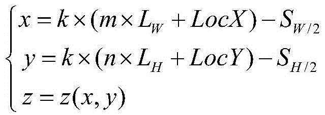
in the formula, x, y and z represent position coordinates of the defect area in a workpiece coordinate system; m and n represent the numbers of the sub-aperture images corresponding to the defect areas; LocX, LocY denote the pixel coordinates of the defect region in the sub-aperture image; l isW、LHRespectively representing the pixel width and height of the sub-aperture image; sW/2、SH/2Respectively representing half of the width value and half of the height value of a preset scanning area; k denotes a conversion coefficient of the pixel coordinate system and the object coordinate system.
In this embodiment, optionally, in the second step, the minimum circumscribed circle diameter enveloping all the pixel points in each defective region image is used as the pixel size of each defective region, and then the actual size of the defective region is obtained through the calibrated physical size calculation represented by one pixel.
In this embodiment, optionally, the first step further includes: after obtaining a plurality of defect area images, identifying the defect area on the surface of the element by using an integrated decision tree classification model, removing a rear surface pseudo defect area image and reserving a front surface defect area image.
In this embodiment, optionally, the step two is followed by a step three: and outputting the position and the actual size of the defect area on the surface of the element as a dark field detection file, and setting an individual number for each defect area.
Another embodiment of the invention provides a process method for accurately detecting micro defects on the surface of a large-caliber element, wherein the structural schematic diagram of a detection device is shown in fig. 1, the device comprises a high-precision motion platform and a dark field detection system, the motion platform is used for carrying an optical element to realize scanning and photographing, and the dark field detection system is used for forming a dark field detection environment and collecting a dark field image. When surface micro-defect detection is carried out, firstly, a corresponding scanning photographing track is generated according to the type of an element, the surface of the large-caliber element is scanned by controlling the movement of a motion platform, and a dark field image of the element is obtained; processing the dark field image to acquire position and size information of the surface defect while scanning; and finally, optimizing the defect positioning path and generating a final dark field detection file. The method comprises the following specific steps:
according to the embodiment of the invention, the positioning precision of the motion platform is +/-10 microns, the motion platform comprises X, Y, Z three motion axes, the motion directions of the motion axes are respectively consistent with the directions of X, Y, Z coordinate axes of a machine tool coordinate system, the motion platform can be loaded with an optical large-caliber element to realize the movement along the X, Y axis direction, and the motion platform is loaded with a dark field detection system to realize the movement along the Z axis direction. Before scanning the element, the motion platform is first initialized, including zeroing and error compensation of the axes of the platform, and the machine coordinate system is determined through the process. And after the platform is initialized, moving to a mounting station to complete the mounting of the element.
Step 2, performing dark field scanning and photographing on the element by using a dark field detection system;
according to the embodiment of the invention, the dark field detection system is composed of an area-array camera, a telecentric lens and an annular light source, and the structural schematic diagram of the dark field detection system is shown in fig. 2. The resolution of the area-array camera is 5120 × 5120, and the pixel size is 4.5 μm × 4.5 μm. In order to realize distortion-free detection of surface defects of the elements, a double telecentric lens is selected, the magnification of the lens is 0.46, and the working distance is 180mm +/-3%. In order to form a dark field detection environment, an annular light source is adopted to irradiate the surface of the optical element at a low angle, and the brightness and the on-off state of the light source are automatically adjusted through a light source controller.
The detected surface of the element comprises a plane and an aspheric surface, the Z-axis coordinate of a photographing point is required to be determined according to the type of the element, and the S-shaped scanning path is suitable for the plane and the aspheric surface and is an S-shaped scanning path on an X-Y plane so as to ensure that a dark field camera can obtain a full aperture image of the element while focusing clearly. In order to improve the scanning efficiency, the scanning device adopts an S-shaped scanning path, realizes the progressive scanning of elements by controlling the motion platform to move along the X, Y axis, and adjusts the object distance by controlling the motion platform to move along the Z axis so as to ensure the clear collected dark field image.
Under the conditions of 4.5 μm pixel size and 0.46 lens magnification, the defect resolution detectable by the camera is 4.5/0.46-9.78 μm, and the camera field of view is 50mm × 50 mm. The size of the optical element is 430mm × 430mm, when full aperture scanning is carried out, a total of 81 subgraphs are needed, 9 × 9, and the scanning area is 450mm × 450 mm. Scanning is carried out along the row direction by taking the point S in the figure 2 as a starting point, 9 pictures are scanned in each row, 9 rows are scanned in total, a subgraph is named in a format of Xm-Yn, n represents a row number, and m represents the mth image of the nth row. The position of the photographed spot is as follows (1):

in the formula, xi,j、yi,j、zi,jThe coordinate of the machine tool at the ith sub-image photographing position of the jth row is in mm; x is the number ofo、yoThe machine tool coordinate is the machine tool coordinate when the element center point moves to the dark field detection station; xs and Ys are scanning stepping values in the X, Y direction, and are both 50 mm; sX、SYThe distance from the scanning starting point to the geometric center of the element is 200 mm; z (x, y) is an element surface equation with the element center as the origin of coordinates, including both planar and aspheric; z is a radical ofoIs the machine z coordinate when the dark field camera is in focus at the center of the element.
In order to improve the scanning and photographing efficiency of the area-array camera and ensure the quality of the collected images, the motion track and the speed of the platform in the scanning process are planned as follows:
(1) in order to reduce the scanning time, the platform is controlled to move at a higher speed before the platform is moved to the photographing position, and meanwhile, the S-shaped path in FIG. 2 is adopted to scan and photograph the optical element;
(2) in order to ensure the quality of the collected image, when the platform moves to a photographing position, the platform is decelerated to zero, and the camera is controlled to automatically collect the image;
(3) and (3) after the clear image of the photographing position is obtained, controlling the platform to continuously move, and repeating the processes (1) and (2) until the surface of the whole element is scanned.
Step 3, processing the dark field image to obtain position and size information of the defect;
according to the embodiment of the invention, firstly, the image is segmented to extract the defect part, because the back surface of the element has defects and pseudo defect points with larger sizes, the interference of the back surface defects is eliminated by using an integrated decision tree, and then, the positions and the pixel sizes of the defect points in the image are obtained by calculating the minimum circumcircle of the defects. And obtaining the actual coordinates of the defect point positioned to each station of the platform by establishing the conversion relation from the pixel coordinates to the machine tool coordinates, and obtaining the actual size of the defect point by calibrating the actual size represented by a single pixel.
The image processing aims at element sub-image images, 81 images are required to be acquired after the surface scanning of the large-caliber element is completed, the resolution of each image is 5120 x 5120, the pixels of the spliced images reach 20 hundred million, the requirement on the memory of a computer for processing the spliced images is extremely high, and the processing speed is very low. Therefore, the invention analyzes the sub-image, obtains the position information of the defect in the whole image by calculating the sub-image coordinate, and realizes the synchronous scanning photographing and image processing by adopting the multi-thread programming, thereby improving the processing efficiency.
The method comprises the following specific steps:
step 3-1: and processing the subgraph obtained by scanning and photographing, and extracting the target point by using a fixed threshold segmentation method. Because the depth of field of the dark field detection system is larger, the defect positioned on the rear surface of the optical element can be imaged in the sub-image to interfere with the extraction of the defect information, and therefore the integrated decision tree is used for distinguishing the front surface defect and the rear surface defect so as to eliminate the interference of a rear surface target point. Calculating the minimum circumcircle of the defect image, taking the center of the circumcircle as the coordinates (LocX, LocY) of the defect in the image, and taking the diameter of the circumcircle as the pixel size L of the defectpixelThe process is shown in fig. 3.
Step 3-2: in the large-aperture optical element scanning, a single-line scanning outputs m to 9 sub-aperture images and n to 9 lines in succession. The sub-aperture image is named in the format "Xm-Yn" during the image acquisition process, and the position of the sub-aperture image in the global scanning range can be determined according to the image number, as shown in fig. 3. In order to determine the position of the defect point in the workpiece coordinate system, the sub-aperture image number Xm-Yn and the coordinates (LocX, LocY) of the defect point in the sub-aperture are obtained, and then the calculation is performed by using the formula (2).

Wherein x, y, z represent the position (mm) of the target defect point in the workpiece coordinate system; m, n represent the coding of the sub-aperture output image; LocX, LocY denote the local coordinates (pixels) of the defect point in the sub-aperture image; l isW、LHThe pixel width/height of the sub-aperture image is 5120 pixel; sW/2、SH/2Represents the half width/height of the scanning area, and is 225 mm;k denotes the conversion factor (mm/pixel) of the dark field acquisition image pixel.
Step 4, generating a dark field detection file;
according to the embodiment of the invention, after the dark field detection is finished, the detection result needs to be output as the dark field detection file, the file sets an independent number for each defect, and stores the information such as the position, the size and the like of the defect point, so that a reliable basis can be provided for the subsequent defect point positioning and repairing process. The format of the dark field detection file is shown in fig. 4, and all target points obtained by dark field detection are numbered so as to facilitate finding and tracking of defects; because the subsequent process needs to position the defect points one by one, in order to shorten the positioning distance, the invention plans the path by using a greedy algorithm according to the coordinates of the defect points, and the defect points are numbered according to the sequence of the path; and recording target point information by taking the number as a unit, wherein the target point information comprises a sub-image number where the target point is located, target point pixel coordinates, actual coordinates and a target point size.
Another embodiment of the present invention provides an example analysis of a precise detection process for surface micro-defects of large-caliber components, which is used to detect a batch of large-caliber components with caliber 430mm × 430mm and a plane detection surface. The detection process is carried out on autonomously developed automatic detection and repair control software for the surface defects of the large-caliber fused quartz element, and the specific process is as follows:
(1) and calculating the position of a photographing point of dark field scanning according to the formula (1), controlling the motion platform and the dark field detection system to scan and photograph the element, and acquiring 81 pictures. The 81 pictures can cover the entire optical element surface, and the stitched image is numbered according to the rows and columns of the subgraphs as shown in fig. 5.
(2) And processing the image, segmenting a target point by binarization, and removing a rear surface point detected by a dark field by using a classification model based on a decision tree. FIG. 6 is an image processing procedure of a partial region of a sub-image, the region includes (i) eight target points, (ii) eight target points, (iii) eight target points are rear edge plane points, and the target points can be eliminated through the processing procedure; and solving the minimum circumcircle of the other seven points, taking the center of the minimum circumcircle as the coordinate of the defect, and converting the minimum circumcircle into the actual coordinate of the workpiece coordinate system.
(3) And saving the result in a fixed format into a dark field detection file.
The method realizes the accurate detection of the micro-defects on the surface of the large-caliber element through the steps, and can provide accurate position coordinates and size information for the positioning and repairing of subsequent defect points.
While the invention has been described with respect to a limited number of embodiments, those skilled in the art, having benefit of this description, will appreciate that other embodiments can be devised which do not depart from the scope of the invention as described herein. The present invention has been disclosed in an illustrative rather than a restrictive sense, and the scope of the present invention is defined by the appended claims.
Claims (7)
1. A process method for accurately detecting micro defects on the surface of a large-caliber element is characterized by comprising the following steps:
firstly, performing row-by-row and column-by-column mobile scanning on a preset scanning area on the surface of an element, and acquiring a plurality of sub-aperture images of a plurality of preset photographing positions;
step two, processing the plurality of sub-aperture images to obtain the positions and actual sizes of a plurality of defect areas on the surface of the element; the method comprises the following specific steps:
secondly, performing image segmentation processing on each sub-aperture image to obtain a plurality of defect area images;
secondly, calculating the centers of the minimum circumscribed circles of all pixel points in the image enveloping the defect regions, and taking the centers as pixel coordinates corresponding to each defect region;
calculating according to the size of a preset scanning area, the number of sub-aperture images at a preset photographing position and the pixel coordinates to obtain the position of each defect area;
and step four, calculating the pixel size of the defect area through the calibrated physical size represented by one pixel to obtain the actual size of each defect area.
2. The method for accurately detecting the surface micro-defects of the large-caliber element according to claim 1, wherein in the first step, the surface of the element is irradiated by an annular light source at a low angle to form a dark field environment, and the sub-aperture image is scanned and acquired in the dark field environment.
3. The method as claimed in claim 2, wherein in the step one, during the scanning process, the preset photographing position of each sub-aperture image in the machine coordinate system is set, and the preset photographing position of each sub-aperture image is:

in the formula, xi,j、yi,j、zi,jRepresenting the photographing position of the jth row and ith column sub-aperture image in a machine tool coordinate system; x is the number ofo、yoX, Y axis coordinates in a machine coordinate system when the geometric center point of the element is at the center of the camera visual field; xs and Ys respectively represent scanning stepping values along the row direction and the column direction; sX、SYRespectively representing the distance between the scanning starting point and the geometric center point of the element in the direction of X, Y axes; z (.) represents the surface equation of the element with the geometric center point of the element as the origin of coordinates; z is a radical ofoAnd the Z-axis coordinate of the geometric center point of the element in the machine tool coordinate system when the camera is in clear focus is represented.
4. The method according to claim 3, wherein the position of each defect area in the second step and the third step is calculated according to the following formula:

wherein (x, y, z) represents the coordinates of the defect region on the workpiecePosition coordinates under the system; m and n represent the numbers of the sub-aperture images corresponding to the defect areas; LocX, LocY denote the pixel coordinates of the defect region in the sub-aperture image; l isW、LHRespectively representing the pixel width and height of the sub-aperture image; sW/2、SH/2Respectively representing half of the width value and half of the height value of a preset scanning area; k denotes a conversion coefficient of the pixel coordinate system and the object coordinate system.
5. The precise detection process method for the surface micro-defects of the large-caliber element according to claim 4, wherein in the second step, the diameter of the minimum circumcircle enveloping all pixel points in the image of each defect area is used as the pixel size of each defect area, and then the actual size of the defect area is obtained through the calculation of the physical size represented by a calibrated pixel.
6. The method for accurately detecting the micro-defects on the surface of the large-caliber element according to claim 5, wherein the step two further comprises the following steps: after obtaining a plurality of defect area images, identifying the defect area on the surface of the element by using an integrated decision tree classification model, removing a rear surface pseudo defect area image and reserving a front surface defect area image.
7. The method for accurately detecting the micro-defects on the surface of the large-caliber element according to claim 6, wherein the step two is followed by the step three: and outputting the position and the actual size of the defect area on the surface of the element as a dark field detection file, and setting an individual number for each defect area.
Priority Applications (1)
| Application Number | Priority Date | Filing Date | Title |
|---|---|---|---|
| CN202111429843.XA CN114113116B (en) | 2021-11-29 | 2021-11-29 | Accurate detection process method for surface microdefect of large-caliber element |
Applications Claiming Priority (1)
| Application Number | Priority Date | Filing Date | Title |
|---|---|---|---|
| CN202111429843.XA CN114113116B (en) | 2021-11-29 | 2021-11-29 | Accurate detection process method for surface microdefect of large-caliber element |
Publications (2)
| Publication Number | Publication Date |
|---|---|
| CN114113116A true CN114113116A (en) | 2022-03-01 |
| CN114113116B CN114113116B (en) | 2023-08-18 |
Family
ID=80371136
Family Applications (1)
| Application Number | Title | Priority Date | Filing Date |
|---|---|---|---|
| CN202111429843.XA Active CN114113116B (en) | 2021-11-29 | 2021-11-29 | Accurate detection process method for surface microdefect of large-caliber element |
Country Status (1)
| Country | Link |
|---|---|
| CN (1) | CN114113116B (en) |
Cited By (1)
| Publication number | Priority date | Publication date | Assignee | Title |
|---|---|---|---|---|
| CN114332078A (en) * | 2022-03-02 | 2022-04-12 | 山东华硕汽车配件科技有限公司 | Intelligent repair control method for metal abrasion of automobile engine |
Citations (8)
| Publication number | Priority date | Publication date | Assignee | Title |
|---|---|---|---|---|
| JP2003007243A (en) * | 2001-06-19 | 2003-01-10 | Seiko Instruments Inc | Automatic focusing method for scanning electron microscope having laser defect detection function |
| TW201013963A (en) * | 2008-08-15 | 2010-04-01 | Ulvac Inc | Method and apparatus for manufacturing solar battery |
| CN105181600A (en) * | 2015-09-02 | 2015-12-23 | 哈尔滨工业大学 | Large-aperture curved surface optical element micro-defect detection and laser restoration apparatus |
| CN106018414A (en) * | 2016-05-17 | 2016-10-12 | 浙江大学 | Quantitative detection method for surface defects of optical element with high-order curved surface |
| CN107389688A (en) * | 2017-07-21 | 2017-11-24 | 中国工程物理研究院激光聚变研究中心 | Heavy caliber fused quartz optical component surface microdefect multistation integrates restorative procedure |
| CN110006905A (en) * | 2019-01-25 | 2019-07-12 | 杭州晶耐科光电技术有限公司 | A kind of ultra-clean smooth surface defect detecting device of heavy caliber that line area array cameras combines |
| CN110411346A (en) * | 2019-08-12 | 2019-11-05 | 哈尔滨工业大学 | A kind of aspherical fused quartz element surface microdefect method for rapidly positioning |
| CN110609037A (en) * | 2019-07-12 | 2019-12-24 | 北京旷视科技有限公司 | Product defect detection system and method |
-
2021
- 2021-11-29 CN CN202111429843.XA patent/CN114113116B/en active Active
Patent Citations (8)
| Publication number | Priority date | Publication date | Assignee | Title |
|---|---|---|---|---|
| JP2003007243A (en) * | 2001-06-19 | 2003-01-10 | Seiko Instruments Inc | Automatic focusing method for scanning electron microscope having laser defect detection function |
| TW201013963A (en) * | 2008-08-15 | 2010-04-01 | Ulvac Inc | Method and apparatus for manufacturing solar battery |
| CN105181600A (en) * | 2015-09-02 | 2015-12-23 | 哈尔滨工业大学 | Large-aperture curved surface optical element micro-defect detection and laser restoration apparatus |
| CN106018414A (en) * | 2016-05-17 | 2016-10-12 | 浙江大学 | Quantitative detection method for surface defects of optical element with high-order curved surface |
| CN107389688A (en) * | 2017-07-21 | 2017-11-24 | 中国工程物理研究院激光聚变研究中心 | Heavy caliber fused quartz optical component surface microdefect multistation integrates restorative procedure |
| CN110006905A (en) * | 2019-01-25 | 2019-07-12 | 杭州晶耐科光电技术有限公司 | A kind of ultra-clean smooth surface defect detecting device of heavy caliber that line area array cameras combines |
| CN110609037A (en) * | 2019-07-12 | 2019-12-24 | 北京旷视科技有限公司 | Product defect detection system and method |
| CN110411346A (en) * | 2019-08-12 | 2019-11-05 | 哈尔滨工业大学 | A kind of aspherical fused quartz element surface microdefect method for rapidly positioning |
Cited By (2)
| Publication number | Priority date | Publication date | Assignee | Title |
|---|---|---|---|---|
| CN114332078A (en) * | 2022-03-02 | 2022-04-12 | 山东华硕汽车配件科技有限公司 | Intelligent repair control method for metal abrasion of automobile engine |
| CN114332078B (en) * | 2022-03-02 | 2022-06-10 | 山东华硕汽车配件科技有限公司 | Intelligent repair control method for metal abrasion of automobile engine |
Also Published As
| Publication number | Publication date |
|---|---|
| CN114113116B (en) | 2023-08-18 |
Similar Documents
| Publication | Publication Date | Title |
|---|---|---|
| CN107356608B (en) | Rapid dark field detection method for surface microdefects of large-caliber fused quartz optical element | |
| CN108645867B (en) | Rapid locating and batch detection method for micro defects on surface of large-caliber optical crystal | |
| CN108760766B (en) | Image splicing method for detecting surface micro-defects of large-caliber optical crystal | |
| CN114113114B (en) | Automatic process method for detecting and repairing micro defects on surface of large-caliber element | |
| CN110411346B (en) | Method for quickly positioning surface micro-defects of aspheric fused quartz element | |
| CN113269762B (en) | Screen defect detection method, system and computer storage medium | |
| CN108489986A (en) | A kind of increasing material manufacturing on-line checking and restorative procedure | |
| CN110501347A (en) | A kind of rapid automatized Systems for optical inspection and method | |
| CN113134683A (en) | Laser marking method and device based on machine learning | |
| CN111474179A (en) | Lens surface cleanliness detection device and method | |
| CN114331995A (en) | Multi-template matching real-time positioning method based on improved 2D-ICP | |
| CN113781458A (en) | Artificial intelligence based identification method | |
| CN114113116B (en) | Accurate detection process method for surface microdefect of large-caliber element | |
| CN114113112B (en) | Surface micro defect positioning and identifying method based on three-light-source microscopic system | |
| CN114113115B (en) | High-precision automatic positioning method for micro defects on surface of large-caliber element | |
| CN116109633B (en) | Window detection method and device for bearing retainer | |
| CN108705689B (en) | Automatic tool setting process method for repairing surface microdefects of large-caliber precise optical crystal | |
| CN108833789A (en) | A kind of real-time autofocus and auto focusing method | |
| CN112839168B (en) | Method for automatically adjusting camera imaging resolution in AOI detection system | |
| CN112581424B (en) | Classification extraction method for surface and subsurface defects of optical element | |
| CN113970560A (en) | Defect three-dimensional detection method based on multi-sensor fusion | |
| CN114286078A (en) | Camera module lens appearance inspection method and equipment | |
| CN114120318B (en) | Dark field image target point accurate extraction method based on integrated decision tree | |
| CN112257514B (en) | Infrared vision intelligent detection shooting method for equipment fault inspection | |
| CN114280083B (en) | Detection method for realizing industrial X-ray nondestructive detection of large-size flat castings based on automatic CNC programming of linear array camera |
Legal Events
| Date | Code | Title | Description |
|---|---|---|---|
| PB01 | Publication | ||
| PB01 | Publication | ||
| SE01 | Entry into force of request for substantive examination | ||
| SE01 | Entry into force of request for substantive examination | ||
| GR01 | Patent grant | ||
| GR01 | Patent grant |