CN114088741A - Dual beam microscope system for imaging during sample processing - Google Patents
Dual beam microscope system for imaging during sample processing Download PDFInfo
- Publication number
- CN114088741A CN114088741A CN202110657931.9A CN202110657931A CN114088741A CN 114088741 A CN114088741 A CN 114088741A CN 202110657931 A CN202110657931 A CN 202110657931A CN 114088741 A CN114088741 A CN 114088741A
- Authority
- CN
- China
- Prior art keywords
- sample
- electron beam
- electron
- paragraphs
- diaphragm
- Prior art date
- Legal status (The legal status is an assumption and is not a legal conclusion. Google has not performed a legal analysis and makes no representation as to the accuracy of the status listed.)
- Pending
Links
- 238000003384 imaging method Methods 0.000 title claims abstract description 96
- 238000012545 processing Methods 0.000 title claims abstract description 93
- 230000009977 dual effect Effects 0.000 title abstract description 73
- 238000010894 electron beam technology Methods 0.000 claims abstract description 384
- 238000000034 method Methods 0.000 claims abstract description 253
- 230000008859 change Effects 0.000 claims abstract description 36
- 230000000694 effects Effects 0.000 claims description 118
- 230000000903 blocking effect Effects 0.000 claims description 17
- 238000005530 etching Methods 0.000 claims description 14
- 230000005855 radiation Effects 0.000 claims description 7
- 238000000313 electron-beam-induced deposition Methods 0.000 claims description 3
- 230000008569 process Effects 0.000 abstract description 17
- 230000008021 deposition Effects 0.000 abstract description 13
- 238000000227 grinding Methods 0.000 abstract description 7
- 230000003750 conditioning effect Effects 0.000 abstract description 4
- 239000002245 particle Substances 0.000 description 245
- 230000005672 electromagnetic field Effects 0.000 description 51
- 239000002344 surface layer Substances 0.000 description 22
- 230000005405 multipole Effects 0.000 description 20
- 239000010410 layer Substances 0.000 description 18
- 230000004075 alteration Effects 0.000 description 17
- 230000009471 action Effects 0.000 description 14
- 230000003287 optical effect Effects 0.000 description 13
- 238000011144 upstream manufacturing Methods 0.000 description 13
- 238000000151 deposition Methods 0.000 description 12
- 230000007246 mechanism Effects 0.000 description 12
- 239000011800 void material Substances 0.000 description 9
- 230000000295 complement effect Effects 0.000 description 7
- 238000003917 TEM image Methods 0.000 description 6
- 238000009825 accumulation Methods 0.000 description 6
- 239000011888 foil Substances 0.000 description 6
- 230000004048 modification Effects 0.000 description 6
- 238000012986 modification Methods 0.000 description 6
- 239000013078 crystal Substances 0.000 description 5
- 230000001419 dependent effect Effects 0.000 description 5
- 238000010586 diagram Methods 0.000 description 5
- 238000010438 heat treatment Methods 0.000 description 5
- 230000005428 wave function Effects 0.000 description 5
- 201000009310 astigmatism Diseases 0.000 description 4
- 238000004364 calculation method Methods 0.000 description 4
- 230000001427 coherent effect Effects 0.000 description 4
- 238000000851 scanning transmission electron micrograph Methods 0.000 description 4
- 230000005540 biological transmission Effects 0.000 description 3
- 238000004891 communication Methods 0.000 description 3
- 238000011109 contamination Methods 0.000 description 3
- 238000005421 electrostatic potential Methods 0.000 description 3
- 238000002347 injection Methods 0.000 description 2
- 239000007924 injection Substances 0.000 description 2
- 238000011835 investigation Methods 0.000 description 2
- 239000000463 material Substances 0.000 description 2
- 238000000386 microscopy Methods 0.000 description 2
- 230000004044 response Effects 0.000 description 2
- 238000004458 analytical method Methods 0.000 description 1
- 238000003491 array Methods 0.000 description 1
- 230000015572 biosynthetic process Effects 0.000 description 1
- 150000001875 compounds Chemical class 0.000 description 1
- 238000012937 correction Methods 0.000 description 1
- 238000001514 detection method Methods 0.000 description 1
- 230000005684 electric field Effects 0.000 description 1
- 238000002474 experimental method Methods 0.000 description 1
- 238000005286 illumination Methods 0.000 description 1
- 230000000977 initiatory effect Effects 0.000 description 1
- 238000010884 ion-beam technique Methods 0.000 description 1
- 238000001459 lithography Methods 0.000 description 1
- 238000004519 manufacturing process Methods 0.000 description 1
- 239000000203 mixture Substances 0.000 description 1
- 230000005404 monopole Effects 0.000 description 1
- 230000003647 oxidation Effects 0.000 description 1
- 238000007254 oxidation reaction Methods 0.000 description 1
- 229920001690 polydopamine Polymers 0.000 description 1
- 238000007493 shaping process Methods 0.000 description 1
- 230000003068 static effect Effects 0.000 description 1
- 238000003860 storage Methods 0.000 description 1
- 230000001360 synchronised effect Effects 0.000 description 1
- 238000013169 thromboelastometry Methods 0.000 description 1
- 238000004627 transmission electron microscopy Methods 0.000 description 1
Images


Classifications
-
- H—ELECTRICITY
- H01—ELECTRIC ELEMENTS
- H01J—ELECTRIC DISCHARGE TUBES OR DISCHARGE LAMPS
- H01J37/00—Discharge tubes with provision for introducing objects or material to be exposed to the discharge, e.g. for the purpose of examination or processing thereof
- H01J37/30—Electron-beam or ion-beam tubes for localised treatment of objects
- H01J37/3002—Details
- H01J37/3005—Observing the objects or the point of impact on the object
-
- G—PHYSICS
- G01—MEASURING; TESTING
- G01N—INVESTIGATING OR ANALYSING MATERIALS BY DETERMINING THEIR CHEMICAL OR PHYSICAL PROPERTIES
- G01N23/00—Investigating or analysing materials by the use of wave or particle radiation, e.g. X-rays or neutrons, not covered by groups G01N3/00 – G01N17/00, G01N21/00 or G01N22/00
- G01N23/02—Investigating or analysing materials by the use of wave or particle radiation, e.g. X-rays or neutrons, not covered by groups G01N3/00 – G01N17/00, G01N21/00 or G01N22/00 by transmitting the radiation through the material
- G01N23/04—Investigating or analysing materials by the use of wave or particle radiation, e.g. X-rays or neutrons, not covered by groups G01N3/00 – G01N17/00, G01N21/00 or G01N22/00 by transmitting the radiation through the material and forming images of the material
-
- G—PHYSICS
- G01—MEASURING; TESTING
- G01N—INVESTIGATING OR ANALYSING MATERIALS BY DETERMINING THEIR CHEMICAL OR PHYSICAL PROPERTIES
- G01N23/00—Investigating or analysing materials by the use of wave or particle radiation, e.g. X-rays or neutrons, not covered by groups G01N3/00 – G01N17/00, G01N21/00 or G01N22/00
- G01N23/20—Investigating or analysing materials by the use of wave or particle radiation, e.g. X-rays or neutrons, not covered by groups G01N3/00 – G01N17/00, G01N21/00 or G01N22/00 by using diffraction of the radiation by the materials, e.g. for investigating crystal structure; by using scattering of the radiation by the materials, e.g. for investigating non-crystalline materials; by using reflection of the radiation by the materials
- G01N23/20008—Constructional details of analysers, e.g. characterised by X-ray source, detector or optical system; Accessories therefor; Preparing specimens therefor
-
- G—PHYSICS
- G01—MEASURING; TESTING
- G01N—INVESTIGATING OR ANALYSING MATERIALS BY DETERMINING THEIR CHEMICAL OR PHYSICAL PROPERTIES
- G01N23/00—Investigating or analysing materials by the use of wave or particle radiation, e.g. X-rays or neutrons, not covered by groups G01N3/00 – G01N17/00, G01N21/00 or G01N22/00
- G01N23/20—Investigating or analysing materials by the use of wave or particle radiation, e.g. X-rays or neutrons, not covered by groups G01N3/00 – G01N17/00, G01N21/00 or G01N22/00 by using diffraction of the radiation by the materials, e.g. for investigating crystal structure; by using scattering of the radiation by the materials, e.g. for investigating non-crystalline materials; by using reflection of the radiation by the materials
- G01N23/20058—Measuring diffraction of electrons, e.g. low energy electron diffraction [LEED] method or reflection high energy electron diffraction [RHEED] method
-
- G—PHYSICS
- G01—MEASURING; TESTING
- G01N—INVESTIGATING OR ANALYSING MATERIALS BY DETERMINING THEIR CHEMICAL OR PHYSICAL PROPERTIES
- G01N23/00—Investigating or analysing materials by the use of wave or particle radiation, e.g. X-rays or neutrons, not covered by groups G01N3/00 – G01N17/00, G01N21/00 or G01N22/00
- G01N23/20—Investigating or analysing materials by the use of wave or particle radiation, e.g. X-rays or neutrons, not covered by groups G01N3/00 – G01N17/00, G01N21/00 or G01N22/00 by using diffraction of the radiation by the materials, e.g. for investigating crystal structure; by using scattering of the radiation by the materials, e.g. for investigating non-crystalline materials; by using reflection of the radiation by the materials
- G01N23/20083—Investigating or analysing materials by the use of wave or particle radiation, e.g. X-rays or neutrons, not covered by groups G01N3/00 – G01N17/00, G01N21/00 or G01N22/00 by using diffraction of the radiation by the materials, e.g. for investigating crystal structure; by using scattering of the radiation by the materials, e.g. for investigating non-crystalline materials; by using reflection of the radiation by the materials by using a combination of at least two measurements at least one being a transmission measurement and one a scatter measurement
-
- G—PHYSICS
- G01—MEASURING; TESTING
- G01N—INVESTIGATING OR ANALYSING MATERIALS BY DETERMINING THEIR CHEMICAL OR PHYSICAL PROPERTIES
- G01N23/00—Investigating or analysing materials by the use of wave or particle radiation, e.g. X-rays or neutrons, not covered by groups G01N3/00 – G01N17/00, G01N21/00 or G01N22/00
- G01N23/20—Investigating or analysing materials by the use of wave or particle radiation, e.g. X-rays or neutrons, not covered by groups G01N3/00 – G01N17/00, G01N21/00 or G01N22/00 by using diffraction of the radiation by the materials, e.g. for investigating crystal structure; by using scattering of the radiation by the materials, e.g. for investigating non-crystalline materials; by using reflection of the radiation by the materials
- G01N23/205—Investigating or analysing materials by the use of wave or particle radiation, e.g. X-rays or neutrons, not covered by groups G01N3/00 – G01N17/00, G01N21/00 or G01N22/00 by using diffraction of the radiation by the materials, e.g. for investigating crystal structure; by using scattering of the radiation by the materials, e.g. for investigating non-crystalline materials; by using reflection of the radiation by the materials using diffraction cameras
-
- G—PHYSICS
- G01—MEASURING; TESTING
- G01N—INVESTIGATING OR ANALYSING MATERIALS BY DETERMINING THEIR CHEMICAL OR PHYSICAL PROPERTIES
- G01N23/00—Investigating or analysing materials by the use of wave or particle radiation, e.g. X-rays or neutrons, not covered by groups G01N3/00 – G01N17/00, G01N21/00 or G01N22/00
- G01N23/20—Investigating or analysing materials by the use of wave or particle radiation, e.g. X-rays or neutrons, not covered by groups G01N3/00 – G01N17/00, G01N21/00 or G01N22/00 by using diffraction of the radiation by the materials, e.g. for investigating crystal structure; by using scattering of the radiation by the materials, e.g. for investigating non-crystalline materials; by using reflection of the radiation by the materials
- G01N23/2055—Analysing diffraction patterns
-
- G—PHYSICS
- G01—MEASURING; TESTING
- G01N—INVESTIGATING OR ANALYSING MATERIALS BY DETERMINING THEIR CHEMICAL OR PHYSICAL PROPERTIES
- G01N23/00—Investigating or analysing materials by the use of wave or particle radiation, e.g. X-rays or neutrons, not covered by groups G01N3/00 – G01N17/00, G01N21/00 or G01N22/00
- G01N23/20—Investigating or analysing materials by the use of wave or particle radiation, e.g. X-rays or neutrons, not covered by groups G01N3/00 – G01N17/00, G01N21/00 or G01N22/00 by using diffraction of the radiation by the materials, e.g. for investigating crystal structure; by using scattering of the radiation by the materials, e.g. for investigating non-crystalline materials; by using reflection of the radiation by the materials
- G01N23/207—Diffractometry using detectors, e.g. using a probe in a central position and one or more displaceable detectors in circumferential positions
-
- G—PHYSICS
- G01—MEASURING; TESTING
- G01N—INVESTIGATING OR ANALYSING MATERIALS BY DETERMINING THEIR CHEMICAL OR PHYSICAL PROPERTIES
- G01N23/00—Investigating or analysing materials by the use of wave or particle radiation, e.g. X-rays or neutrons, not covered by groups G01N3/00 – G01N17/00, G01N21/00 or G01N22/00
- G01N23/22—Investigating or analysing materials by the use of wave or particle radiation, e.g. X-rays or neutrons, not covered by groups G01N3/00 – G01N17/00, G01N21/00 or G01N22/00 by measuring secondary emission from the material
- G01N23/2202—Preparing specimens therefor
-
- G—PHYSICS
- G01—MEASURING; TESTING
- G01N—INVESTIGATING OR ANALYSING MATERIALS BY DETERMINING THEIR CHEMICAL OR PHYSICAL PROPERTIES
- G01N23/00—Investigating or analysing materials by the use of wave or particle radiation, e.g. X-rays or neutrons, not covered by groups G01N3/00 – G01N17/00, G01N21/00 or G01N22/00
- G01N23/22—Investigating or analysing materials by the use of wave or particle radiation, e.g. X-rays or neutrons, not covered by groups G01N3/00 – G01N17/00, G01N21/00 or G01N22/00 by measuring secondary emission from the material
- G01N23/2206—Combination of two or more measurements, at least one measurement being that of secondary emission, e.g. combination of secondary electron [SE] measurement and back-scattered electron [BSE] measurement
-
- G—PHYSICS
- G01—MEASURING; TESTING
- G01N—INVESTIGATING OR ANALYSING MATERIALS BY DETERMINING THEIR CHEMICAL OR PHYSICAL PROPERTIES
- G01N23/00—Investigating or analysing materials by the use of wave or particle radiation, e.g. X-rays or neutrons, not covered by groups G01N3/00 – G01N17/00, G01N21/00 or G01N22/00
- G01N23/22—Investigating or analysing materials by the use of wave or particle radiation, e.g. X-rays or neutrons, not covered by groups G01N3/00 – G01N17/00, G01N21/00 or G01N22/00 by measuring secondary emission from the material
- G01N23/225—Investigating or analysing materials by the use of wave or particle radiation, e.g. X-rays or neutrons, not covered by groups G01N3/00 – G01N17/00, G01N21/00 or G01N22/00 by measuring secondary emission from the material using electron or ion
- G01N23/2251—Investigating or analysing materials by the use of wave or particle radiation, e.g. X-rays or neutrons, not covered by groups G01N3/00 – G01N17/00, G01N21/00 or G01N22/00 by measuring secondary emission from the material using electron or ion using incident electron beams, e.g. scanning electron microscopy [SEM]
-
- H—ELECTRICITY
- H01—ELECTRIC ELEMENTS
- H01J—ELECTRIC DISCHARGE TUBES OR DISCHARGE LAMPS
- H01J37/00—Discharge tubes with provision for introducing objects or material to be exposed to the discharge, e.g. for the purpose of examination or processing thereof
- H01J37/02—Details
- H01J37/21—Means for adjusting the focus
-
- H—ELECTRICITY
- H01—ELECTRIC ELEMENTS
- H01J—ELECTRIC DISCHARGE TUBES OR DISCHARGE LAMPS
- H01J37/00—Discharge tubes with provision for introducing objects or material to be exposed to the discharge, e.g. for the purpose of examination or processing thereof
- H01J37/26—Electron or ion microscopes; Electron or ion diffraction tubes
- H01J37/28—Electron or ion microscopes; Electron or ion diffraction tubes with scanning beams
-
- G—PHYSICS
- G01—MEASURING; TESTING
- G01N—INVESTIGATING OR ANALYSING MATERIALS BY DETERMINING THEIR CHEMICAL OR PHYSICAL PROPERTIES
- G01N2223/00—Investigating materials by wave or particle radiation
- G01N2223/03—Investigating materials by wave or particle radiation by transmission
-
- G—PHYSICS
- G01—MEASURING; TESTING
- G01N—INVESTIGATING OR ANALYSING MATERIALS BY DETERMINING THEIR CHEMICAL OR PHYSICAL PROPERTIES
- G01N2223/00—Investigating materials by wave or particle radiation
- G01N2223/045—Investigating materials by wave or particle radiation combination of at least 2 measurements (transmission and scatter)
-
- G—PHYSICS
- G01—MEASURING; TESTING
- G01N—INVESTIGATING OR ANALYSING MATERIALS BY DETERMINING THEIR CHEMICAL OR PHYSICAL PROPERTIES
- G01N2223/00—Investigating materials by wave or particle radiation
- G01N2223/05—Investigating materials by wave or particle radiation by diffraction, scatter or reflection
- G01N2223/056—Investigating materials by wave or particle radiation by diffraction, scatter or reflection diffraction
- G01N2223/0561—Investigating materials by wave or particle radiation by diffraction, scatter or reflection diffraction diffraction cameras
-
- G—PHYSICS
- G01—MEASURING; TESTING
- G01N—INVESTIGATING OR ANALYSING MATERIALS BY DETERMINING THEIR CHEMICAL OR PHYSICAL PROPERTIES
- G01N2223/00—Investigating materials by wave or particle radiation
- G01N2223/05—Investigating materials by wave or particle radiation by diffraction, scatter or reflection
- G01N2223/056—Investigating materials by wave or particle radiation by diffraction, scatter or reflection diffraction
- G01N2223/0565—Investigating materials by wave or particle radiation by diffraction, scatter or reflection diffraction diffraction of electrons, e.g. LEED
-
- G—PHYSICS
- G01—MEASURING; TESTING
- G01N—INVESTIGATING OR ANALYSING MATERIALS BY DETERMINING THEIR CHEMICAL OR PHYSICAL PROPERTIES
- G01N2223/00—Investigating materials by wave or particle radiation
- G01N2223/05—Investigating materials by wave or particle radiation by diffraction, scatter or reflection
- G01N2223/056—Investigating materials by wave or particle radiation by diffraction, scatter or reflection diffraction
- G01N2223/0566—Investigating materials by wave or particle radiation by diffraction, scatter or reflection diffraction analysing diffraction pattern
-
- G—PHYSICS
- G01—MEASURING; TESTING
- G01N—INVESTIGATING OR ANALYSING MATERIALS BY DETERMINING THEIR CHEMICAL OR PHYSICAL PROPERTIES
- G01N2223/00—Investigating materials by wave or particle radiation
- G01N2223/07—Investigating materials by wave or particle radiation secondary emission
- G01N2223/071—Investigating materials by wave or particle radiation secondary emission combination of measurements, at least 1 secondary emission
-
- G—PHYSICS
- G01—MEASURING; TESTING
- G01N—INVESTIGATING OR ANALYSING MATERIALS BY DETERMINING THEIR CHEMICAL OR PHYSICAL PROPERTIES
- G01N2223/00—Investigating materials by wave or particle radiation
- G01N2223/10—Different kinds of radiation or particles
- G01N2223/102—Different kinds of radiation or particles beta or electrons
Landscapes
- Chemical & Material Sciences (AREA)
- Analytical Chemistry (AREA)
- Physics & Mathematics (AREA)
- Health & Medical Sciences (AREA)
- Life Sciences & Earth Sciences (AREA)
- Biochemistry (AREA)
- General Health & Medical Sciences (AREA)
- General Physics & Mathematics (AREA)
- Immunology (AREA)
- Pathology (AREA)
- Crystallography & Structural Chemistry (AREA)
- Analysing Materials By The Use Of Radiation (AREA)
- Electron Beam Exposure (AREA)
Abstract
A dual beam microscope system for imaging during sample processing. According to the present disclosure, a method for simultaneously processing a sample and imaging a processed portion of the sample using a dual beam microscope system comprises the initial steps of: emitting a plurality of electrons toward the sample; separating the plurality of electrons into two electron beams; and subsequently modifying the focusing characteristics of at least one of the electron beams such that the two electron beams have different focal planes. Once the two electron beams have different focal planes, the first electron beam is focused such that the first electron beam acts as a STEM beam. The STEM beam is then used to process a region of the sample to cause a physical change (e.g., perform grinding, deposition, charge conditioning, phase change, etc.). Focusing the second electron beam to act as a TEM beam to image the region of the sample being processed.
Description
Background
Charged particle microscopes are used to perform many sample processing applications, including circuit editing and material analysis. However, real-time imaging during sample processing cannot be achieved using current charged particle microscope systems. The inability to monitor the sample area being processed means that incidental growth/etch or processing errors cannot be diagnosed and/or corrected until the end of the process. For example, depending on the sample composition and the atmosphere of the vacuum chamber, there may be incidental deposition, etching and/or oxidation during sample processing, which the user cannot realize until sample processing stops.
This inability to monitor the sample while it is being processed fundamentally limits the usefulness of charged particle microscopy for sample processing, since current users either need to accept inaccurate performance or significantly reduce production time by regularly stopping sample processing for imaging. Therefore, there is a need for a system that can simultaneously process a sample and image a region of the sample.
Disclosure of Invention
According to the present disclosure, a method for simultaneously processing a sample and imaging a processed portion of the sample using a dual beam microscope system comprises the initial steps of: emitting a plurality of electrons toward the sample; separating the plurality of electrons into a first electron beam and a second electron beam; and subsequently modifying the focusing characteristics of at least one of the first and second electron beams such that the two electron beams have different focal planes. Once the two beams have different focal planes, the method according to the invention comprises the additional step of focusing the first electron beam such that the first electron beam acts as a STEM beam focused at the sample. The STEM beam is then used to process a region of the sample to cause a physical change (e.g., perform grinding, deposition, etching, contamination growth, charge conditioning, radiation damage, sample deformation, heating, phase change, etc.).
The method further includes focusing the second electron beam such that the second electron beam acts as a TEM beam for imaging the region of the sample being processed so that a user can view the physical changes of the sample in real or near real time. In some embodiments, the relative angles at which the STEM beam and the TEM beam are incident on the sample are such that the STEM beam and/or sample emissions produced by the STEM beam are blocked by a beam blocker, thereby enabling a detector to at least initially detect the TEM beam and/or sample emissions produced by the TEM beam. The method can include deflecting the STEM beam using a beam deflector such that the STEM beam is no longer detected (e.g., such that the STEM beam is blocked by a beam blocker, or moved outside of a field of view of a detector system). In this way, when the STEM beam is deflected, the TEM beam and/or sample emissions produced by the TEM beam can be used to produce images without interference from the STEM beam and/or sample emissions produced by the STEM beam.
Alternatively or additionally, image processing techniques may be used to distinguish the STEM beams and/or sample emissions produced by the STEM beams from the TEM beams and/or sample emissions produced by the TEM beams. In this manner, the image processing techniques are capable of isolating the TEM beam and/or sample emissions produced by the TEM beam so that a TEM image of the processed region of the sample can be formed.
Drawings
The detailed description is made with reference to the accompanying drawings. In the drawings, the left-most digit or digits of a reference number identify the figure in which the reference number first appears. The use of the same reference symbols in different drawings indicates similar or identical items.
FIG. 1 illustrates an example dual beam system for imaging a processing portion of a sample while processing the sample in accordance with this disclosure.
Fig. 2 illustrates an example embodiment of an imaging beam and a processing beam simultaneously interacting with a sample during investigation of the sample by a dual beam system.
Fig. 3 is a sample process for simultaneously processing and imaging a sample according to the present invention.
Fig. 4 is a diagram of etching a sample with a processing beam while imaging the sample with an imaging beam according to the present invention.
FIG. 5 is a diagram of a processing beam used to perform gas-assisted deposition on a sample and an imaging beam used to image the sample.
Fig. 6 shows the optical performance of a bifocal multibeam system according to the present invention.
Fig. 7 illustrates an example dual focus multi-beam system for studying a sample, wherein the dual focus beam shaper comprises a MEMS device.
FIG. 8 illustrates an exemplary MEMS device in accordance with the present invention.
FIG. 9 illustrates a schematic top view of an example embodiment of a MEMS device comprising four electrodes.
FIG. 10 illustrates a schematic top view of an example embodiment of a MEMS device comprising seven electrodes.
Fig. 11 illustrates distortion of the second electron beam caused when the example embodiment bifocal beam shaper causes at least one quadrupole lens effect to be applied thereto.
Fig. 12 illustrates an exemplary embodiment of a bifocal multi-beam system for studying a specimen, wherein the bifocal beam shaper comprises an array of diaphragm lenses.
Fig. 13 illustrates example electrodes of an example stop lens array.
Fig. 14 illustrates an example diaphragm defining structure of an example diaphragm lens array.
FIG. 15 illustrates a cross-section of an example aperture lens array with one aperture defining structure.
16-24 illustrate example central structures that may be used in the multi-stop assembly illustrated in FIG. 23.
Fig. 25 illustrates a cross-section of an example aperture lens array including a first electrode, a second electrode, and an aperture defining structure.
Fig. 26 illustrates an example embodiment of a dual focus multiple beam system for studying a sample, wherein the dual focus beam shaper comprises a beam splitting mechanism and one or more focusing devices.
Like reference numerals designate corresponding parts throughout the several views of the drawings. In general, in the figures, elements that may be included in a given example are illustrated in solid lines, while optional elements for the given example are illustrated in dashed lines. However, elements shown in solid lines are not necessary for all examples of the disclosure, and elements shown in solid lines may be omitted from a particular example without departing from the scope of the disclosure.
Detailed Description
Included herein are methods and systems for simultaneously processing a sample and imaging a processed portion of the sample using a dual beam microscope system. More specifically, the methods and systems disclosed herein include and/or are configured to allow a charged particle microscope to perform TEM imaging of a sample with a first beam while causing a physical change on the sample with a second beam. In the method and system, a plurality of electrons emitted by an electron source are split into a first electron beam and a second electron beam, and a focusing characteristic of at least one of the first electron beam and the second electron beam is modified such that corresponding focal planes of the first electron beam and the second electron beam are different. The two beams may then be focused and/or oriented such that a first electron beam (e.g., an imaging beam) is incident on the sample, while a second electron beam (e.g., a processing beam) causes a desired physical change in the surface of the sample. Example physical changes may include, but are not limited to, grinding, deposition, etching, contamination growth, charge conditioning, radiation damage, sample deformation, heating, phase change, and the like. This allows the processing of the sample to be monitored and adjusted to correct for errors, incidental growth, incidental grinding, incidental deposition, and the like.
In various embodiments, the microscope system may include at least one beam blocker that causes one of the two beams, both of the two beams, or neither beam to be blocked. For example, a beam stop can be positioned below the sample to block the STEM beam. Alternatively or additionally, a beam blocker may also be positioned over the sample such that it selectively blocks one or both of the two beams. One or more beam blockers may be fixed or capable of being moved in position to temporarily block the desired beam or a combination thereof. In some embodiments, a beam stop may be used to prevent the imaging beam and/or emissions generated by the imaging beam incident on the sample from reaching the detector. For example, the imaging beam may be incident on the sample at an oblique angle such that the imaging beam and/or emissions resulting from the imaging beam incident on the sample are prevented from reaching the detector by a beam stop or objective aperture located downstream of the sample. Further, in some embodiments, the beam stop may be positioned such that: when the beam is deflected, the beam blocker blocks the deflected beam.
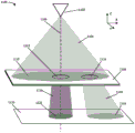
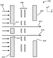
Fig. 1 is a diagram of one or more dual focus multi-beam systems 100 arranged to simultaneously process a sample while also imaging a processed portion of the sample, in accordance with the present invention. In particular, fig. 1 illustrates one or more example dual focus multi-beam systems 102 for simultaneously processing and imaging a sample 104. The one or more example dual focus multi-beam systems 102 may include an Electron Microscope (EM) setup or an electron lithography setup configured to illuminate and/or otherwise impinge a sample 104 with an imaging beam (e.g., a TEM beam) and a processing beam (e.g., a STEM beam). In various embodiments, the one or more bifocal multi-beam systems 102 can be or include one or more different types of EM and/or charged particle microscopes, such as, but not limited to, Scanning Electron Microscopes (SEM), Scanning Transmission Electron Microscopes (STEM), Transmission Electron Microscopes (TEM), Charged Particle Microscopes (CPM), dual-beam microscope systems, and the like. Additionally, in some embodiments, the one or more dual focus multi-beam systems 102 may also be TEMs capable of operating as STEM.
One or more example dual-focus multi-beam systems 102 include an electron source 106 (e.g., a thermal electron source, a Schottky-emission source, a field emission source, etc.) that emits a plurality of electrons 108 (i.e., an electron beam) along an emission axis 110 and toward a dual-focus beam shaper 112. The emission axis 110 is a central axis that extends from the electron source 106 and through the sample 104 along the length of one or more exemplary dual focus multi-beam systems 102.
The dual-focus beamformer 112 is one or more structures configured to: (i) splitting the plurality of electrons 108 into at least a first electron beam 114 and a second electron beam 116; and (ii) modify the focusing characteristics of at least one of the first and second electron beams 114, 116 such that one of the two beams becomes an imaging beam (i.e., a beam that is focused and oriented to produce an image of a region of the sample 104) and the other beam becomes a processing beam (i.e., a beam that is focused and oriented to cause a physical change in the sample 104). In fig. 1, the imaging beam is shown as a TEM beam and the treatment beam is shown as a STEM beam. For example, the dual-focus beam shaper 112 may modify the focusing characteristics such that the first electron beam 114 and the second electron beam 116 have different corresponding focal planes. Fig. 1 illustrates a dual-focus beam shaper 112 that separates the plurality of electrons 108 into a first electron beam 114 and a second electron beam 116 extending along an emission axis 110. Because each of the first and second electron beams 114, 116 is formed by the plurality of electrons 108, the first and second electron beams 114, 116 are coherent with each other.
Fig. 1 also shows a dual-focus beam shaper 112 that applies a distortion to the second electron beam 116 that results in a focusing characteristic of the second electron beam that is different from a focusing characteristic of the first electron beam 114. In particular, fig. 1 illustrates a bifocal beam shaper 112 that is configured to generate at least one quadrupole field (i.e., dipole field, quadrupole field, hexapole field, octopole field, etc.) that applies a quadrupole lens effect that affects the second electron beam 116 such that the two beams have different focusing characteristics. The quadrupole lens effect can distort, astigmatism-free, or otherwise modify at least one of the beams such that the corresponding focusing characteristics of the beams are different. In some embodiments, the quadrupole lens effect may impose a different lens effect in one meridian plane (e.g., the x-z plane) than in a perpendicular meridian plane (e.g., the y-z plane), thereby causing a different change in each of the focal properties of each of the two meridian planes. This stigmation is illustrated in the example system shown in fig. 6.
In such embodiments, a multipole element (e.g., a stigmator) downstream of the bifocal beam shaper may apply a complementary quadrupole lens effect to one of the second electron beams 116 to correct for aberrations introduced by the bifocal beam shaper 112 and to cause the second electron beam 116 to become a cylindrically symmetric beam again. In this way, the multipole element gives the second electron beam 116 cylindrical symmetry downstream of this multipole element, while also having a different focal plane than the first electron beam 114. In various arrangements, this multipole element may be placed in the focal plane of the first electron beam 114 such that the complementary quadrupole lens effect is not applied to the first electron beam 114.
In some embodiments, the dual-focus beam shaper 112 is configured to modify a focusing characteristic of at least one of the first and second electron beams 114, 116 such that the second electron beam 116 is a STEM beam (i.e., has a focal plane at a sample plane at or near the specimen 104), and the first electron beam 114 is a TEM beam (i.e., has a corresponding focal plane such that the first electron beam 114 is parallel, substantially parallel, or slightly converging at the sample plane at or near the specimen 104). In various embodiments, the dual-focus beam shaper 112 may modify the focal plane of the first electron beam 114 such that the focal plane is focused at a plane located at least 0.1%, 1%, 10%, or 100% higher than the upper objective 128 by the objective focal length. Alternatively or additionally, the dual-focus beam shaper 112 may be configured to modify a focusing characteristic of at least one of the first and second electron beams 114, 116 such that a diameter of the first electron beam 114 at a sample plane at or near the specimen 104 is at least one of 20 times, 50 times, 100 times, 500 times, or 1000 times larger than a diameter of the second electron beam 116 at the sample plane. In such embodiments, the dual-focus beam shaper 112 may cause the diameter of the first electron beam 114 to be at least one of 20 times, 50 times, 100 times, 500 times, or 1000 times larger than the diameter of the second electron beam 116 at any plane at which the second electron beam 116 is focused. In some embodiments, the dual-focus beam shaper 112 further deflects one or both of the first and second electron beams 114, 116 away from the emission axis 110.
Alternatively, the dual-focus beam shaper 112 may modify the focusing characteristics of at least one of the electron beams such that the first electron beam 114 is a STEM beam (i.e., has a focal plane at a sample plane at or near the specimen 104) and the second electron beam 116 is a TEM beam (i.e., has a corresponding focal plane such that the first electron beam 114 is parallel, substantially parallel, or slightly converging at the sample plane at or near the specimen 104). In such embodiments, one or more focal planes may be modified such that the second electron beam 116 is focused at a plane located at least 0.1%, 1%, 10%, or 100% above the sample 104 at the focal length of the objective lens.
Although fig. 1 illustrates an embodiment in which the dual-focus beam shaper 112 is shown as modifying the focusing characteristics of the second electron beam 116, in other embodiments, the dual-focus beam shaper 112 may cause the focusing characteristics of the first electron beam 114 or both beams to change such that both beams become the imaging beam and the processing beam. That is, those skilled in the art will appreciate that in various embodiments, actions or effects described as being applied to one beam may be applied to the other beam to cause both beams to become the imaging and processing beams. In various embodiments, the dual focus beamformer 112 or another component of the dual focus multi-beam system 102 may apply deflections to one or both of the beams to make the beams act as both imaging and processing beams.
In some embodiments, the dual-focus beam shaper 112 may be comprised of a single component that performs the formation of the first and second electron beams 114, 116 and the modification of the focal characteristics of at least one of the two beams. For example, the dual-focus beam shaper 112 may correspond to a micro-electro-mechanical system (MEMS) that both forms two beams and generates at least a quadrupole electromagnetic field (i.e., dipole field, quadrupole field, hexapole field, octopole field, etc.) that applies at least one quadrupole lens effect that focuses, astigmatism-cancels, and/or otherwise modifies at least one of the beams such that the corresponding focusing characteristics of the beams are different. In another example, the bifocal beamformer 112 may correspond to an aperture array including a structure defining a plurality of apertures and/or cavities that both form two beams and at least one quadrupole electromagnetic field that imparts a quadrupole lens effect to one or more of the two beams. In some embodiments, the quadrupole lens effect may apply a positive lens in one meridional plane (e.g., the x-z plane) and a negative lens effect in a perpendicular meridional plane (e.g., the y-z plane), resulting in a different change in each of the focal properties of each of the two meridional planes.
In such systems, a multipole element 124 (e.g., a corrector, a stigmator or multipole element that is part of an aberration corrector, a quadrupole/octupole corrector, etc.) that is further downstream to apply a complementary quadrupole lens effect to re-cylindrically symmetric the beams may be included in one or more example bifocal multibeam systems 100. For example, fig. 1 illustrates one or more dual focus multi-beam systems 102 that include an stigmator. Alternatively or additionally, the dual focus beamformer 112 may be positioned and/or configured to cause at least one of one or more aberrations of the electron beams to correct another aberration in the one or more dual focus multi-beam systems 102. This system component may be positioned in the focal plane of the electron beam, to which the dual-focus beamformer 112 does not apply at least one quadrupole lens effect. In embodiments where the dual-focus beam shaper applies at least one first quadrupole lens effect to the first electron beam 114 and at least one second quadrupole lens effect to the second electron beam 116, such one or more dual-focus multi-beam systems 100 may comprise a first multipole element 124 positioned in a focal plane of the first electron beam 114 and configured to apply a complementary quadrupole lens effect to the second electron beam 116 and a second multipole element 124 positioned in a focal plane of the second electron beam 116 and configured to apply a complementary quadrupole lens effect to the first electron beam 114.
Alternatively, the dual focus beamformer 112 may be comprised of a plurality of components 118. A separate component 118 may perform one of forming the first and second electron beams 114, 116 and modifying the focus characteristics of at least one of the two beams, or a separate component may facilitate one or both of forming the beams and modifying the focus characteristics in concert with the other component 118. In some embodiments, the separate components 118 may include physical structures that block a portion of the plurality of electrons 108 while allowing other passage, double prisms (e.g., charged wires), a split-electron beam splitter made of a thin crystal or a grating fabricated on a nanometer scale, a split-beam laser system configured to separate the plurality of electrons 108 into the first and second electron beams 114, 116 using one or more laser mode fringes, and so forth. Alternatively or additionally, the separate component 118 may include one or more lenses (e.g., a single lens, a quadrupole lens, etc.) positioned or otherwise configured to cause the first and second electron beams 114, 116 to have different focal planes. For example, the dual-focus beam shaper 112 may be comprised of a physical structure defining two apertures, and a lens positioned and/or configured to adjust the focusing characteristics of at least one of the first and second electron beams such that the beams have different corresponding focal planes. In various embodiments, the lens may be positioned above or below the physical structure.
Fig. 1 illustrates a dual-focus beam shaper 112 positioned upstream of a focusing assembly 120 configured to apply a lens action that focuses at least one of a first electron beam 114 and a second electron beam 116. In addition, the focusing assembly 120 is positioned upstream of the multipole element 124. In one or more example dual focus multiple beam systems 102 shown in fig. 1, the focusing assembly corresponds to an accelerator 122 that accelerates/decelerates, focuses, and/or directs the first and second electron beams 114, 116 toward a focusing column 126. However, in other embodiments, the accelerator 122 may be positioned between the electron source 106 and the bifocal beamformer 112 such that the accelerator 122 accelerates/decelerates, focuses, and/or directs the electrons 108 toward the bifocal beamformer 112, and the bifocal beamformer 112 separates and modifies the focusing characteristics of the electrons 108 at a final energy (e.g., 30 kV). In such embodiments, the focusing assembly 120 may correspond to a lens or other structure configured to apply a lens action that focuses at least one of the first and second electron beams 114, 116.
The focusing column 126 focuses the electron beams 114 and 116 so that they are incident on the sample 104 as imaging beams and processing beams. In particular, fig. 1 shows a focusing column 126 that focuses the second electron beam 116 to be a STEM beam (e.g., a beam having a focal plane at a sample plane at or near the sample 104) and the first electron beam 114 to be a TEM beam (e.g., a parallel, substantially parallel, or slightly converging/diverging beam at a sample plane at or near the sample 104).
Although not shown in fig. 1, those skilled in the art will appreciate that the focusing column 126 may include one or more correctors (e.g., Cs or Cs + Cc aberration correctors), transmission lenses, deflectors (to deflect the imaging beam, the processing beam, and/or both), scan loops, and the like, as needed to enable and/or enhance the study of the sample 104 with the one or more bifocal multi-beam systems 102. For example, the focusing column 126 may include one or more deflectors that scan the processing beam across the surface of the sample without deflecting the imaging beam. Alternatively, such deflection may be caused or assisted by one or more electromagnetic fields (e.g., dipole fields) generated by the multipole element 124 and/or the bifocal beamformer 112. In some embodiments, this dynamic tilt may be caused by a separate detector/detector system in the MEMS device dual focal spot beamformer 112. However, in other embodiments, the dynamic tilt may be caused and/or supplemented by one or more macro-deflector systems (e.g., in the condenser optics). In embodiments where the deflector/deflection force affects two electron beams, the dual focus multi-beam system 102 may be configured to switch rapidly between imaging modes, such that the STEM beam may be deflected while the imaging results of the TEM beam remain unaffected.
Fig. 1 also shows one or more dual focus multi-beam systems 102 comprising an objective lens 128. The objective lens 128 is an optical element that focuses one of the first and second electron beams 114, 116 to a point near or on the specimen 104. The objective lens 128 may include a monopole plate lens, an electromagnetic-electrostatic compound lens, an electrostatic detector objective lens, or another type of objective lens. For example, the objective lens 128 may correspond to a TEM objective lens, wherein the sample is immersed within the TEM objective lens and/or between the sample front and sample back components of the TEM objective lens 136.
Fig. 1 further shows one or more dual focus multi-beam systems 102 comprising a beam blanker 129 configured such that one of the two beams, both of the two beams are blocked, or neither beam is blocked. The beam blanker 129 may comprise a physical structure defining one or more apertures that allow electrons to pass through the beam blanker. For example, the beam blanker 129 may cause deflection of one of the beams such that it is blocked by a blocking structure, such as a structure defining a diaphragm, knife edge, faraday cup, or the like. An example blocking structure may correspond to a single structure defining a single aperture that allows both beams to pass through until the beam blanker 129 (or the dual focus beamformer 112) deflects one of the beams so that it no longer passes through the single aperture. In another embodiment, the blocking structure may define a first aperture that allows the TEM beam to pass through the blocking structure and a second aperture that allows the STEM beam to pass through the blocking structure. Then, one of the two beams may be deflected such that the corresponding beam no longer passes through the corresponding diaphragm in the blocking structure and is thus prevented from passing through the blocking structure (i.e. is blanked). Alternatively, in some embodiments, the blocking structure itself may be translated and/or one of the diaphragms may be blocked, such that one of the beams is prevented from passing through the blocking structure. This allows the microscope system to switch between TEM, STEM and/or simultaneous STEM and TEM modes of operation.
In some embodiments, the bifocal multi-beam system 102 can include at least one beam blocker 131 below the sample 104 that prevents the imaging beam and/or emissions resulting from the processing beam incident on the sample from reaching the detector 132. Alternatively, the processing beam may be incident on the sample at an oblique angle such that the processing beam and/or the emission produced by the imaging beam incident on the sample is partially, largely or completely prevented from reaching the detector 132 by the objective stop. The beam blocker 131 may be fixed or capable of being translated to selectively block the treatment beam and/or emissions produced thereby. In some embodiments, the beam blocker 131 can be a needle positioned between the sample 104 and the detector 132 that blocks unscattered portions of the STEM beam.
Fig. 1 further illustrates one or more dual focus multi-beam systems 102 comprising a sample holder 130 holding a sample 104. As described above, fig. 1 shows a first electron beam 114 as a TEM beam incident on the sample 104 and a second electron beam 116 as a STEM beam. The one or more bifocal multi-beam systems 102 also include a detector 132 (e.g., a camera) positioned in the diffraction plane that is configured to detect the first electron beam 114, the second electron beam 116, diffracted electrons 134 that have passed through the specimen 104 due to the electron beam 114 incident on the specimen 104, and diffracted electrons 135 that have passed through the specimen 104 due to the electron beam 116 incident on the specimen 104. In this manner, sample emitted and/or diffracted electrons produced by the two beams incident on the sample are detected by the single detector 132 and/or the single detector arrays 132 and 140. Thus, detector data from detector 132/detector array 140 may produce a secondary electron image, a TEM image, or both of the sample. For example, in some embodiments, one or more dual focus multiple beam systems 102 can obtain TEM images and STEM images in close succession by first blocking the first beam 114 and then blocking the second beam 116 using the beam blanker 129 without having to switch out and/or otherwise reconfigure the detector system.
Fig. 1 further illustrates one or more dual focus multi-beam systems 102 optionally including one or more computing devices 142. In various embodiments, the one or more computing devices 142 may be configured to determine or generate TEM images and/or STEM images based on detector data from the detector 132 and/or the detector array 140. This may include the ability to separate the detector data portions corresponding to STEM emissions from the detector data portions corresponding to TEM emissions. Additionally, the computer system may be capable of controlling one or more functions of the one or more bifocal multi-beam systems 102, including but not limited to initiation of processes discussed herein, modifying functions of the one or more bifocal multi-beam systems 102, switching between modes, and the like. Those skilled in the art will appreciate that the computing device 142 depicted in fig. 1 is merely illustrative and is not intended to limit the scope of the present disclosure. The computing systems and devices may include any combination of hardware or software that can perform the indicated functions, including computers, network devices, internet appliances, PDAs, wireless telephones, controllers, oscilloscopes, amplifiers, etc. Computing device 142 may also be connected to other devices not shown, or alternatively may operate as a standalone system.
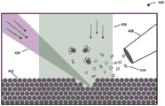
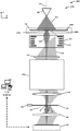
Fig. 2 is an illustration of an imaging beam and a processing beam simultaneously interacting with a sample during investigation of the sample by an example dual focus multi-beam system 100. In particular, fig. 2 illustrates an example embodiment in which first beam 214 is a processing beam focused on a plane at or near the surface of sample 104, and imaging beam 216 is a TEM beam substantially perpendicular to the sample plane at sample 104. However, in other embodiments, the first electron beam 214 may serve as the imaging/TEM illumination beam and the second electron beam 216 may be focused on the surface of the sample to cause the physical change. Fig. 2 also shows a beam blanker 229 that deflects one of the beams so that it is blocked by a blocking structure, such as a structure defining a diaphragm, knife edge, faraday cup, or the like.
A single aperture 201 is defined through which the first beam 214 and the second beam 216 pass. It should be understood that one or more deflectors, multipole elements, dual focal spot beam shapers, or combinations thereof may be used to generate a deflection that deflects one of the first beam 214 or the second beam 216 such that the deflected beam is blanked by the beam blanker 129.
As discussed in the note with respect to fig. 1, the first electron beam 214 may be scanned across the surface of a region of interest of the sample to cause physical changes to the sample. For example, the first e-beam 214 may be used to perform grinding of the sample, etching of the sample (e.g., gas-assisted etching), deposition on the sample (e.g., gas-assisted deposition), causing radiation damage to a region of the sample, causing a phase change to a region of the sample, reducing and/or causing charge accumulation on a region of the sample, heating the sample, deforming the sample, or a combination thereof. For example, when performing cryoelectron microscopy, the first electron beam 214 may be used to reduce sample strain and/or melt a desired portion of the sample. In this way, the user can use the first beam 214 to relieve high stress on the sample without damaging the area of interest, and then use the second electron beam 216 to produce the final image. In another example, the first electron beam 214 may be used to induce a phase change over a region of the sample. Such phase change patterns may be created using the first electron beam 214 to perform various functions, such as aberration correction.
In another example use case, the bifocal multi-beam system 100 can include an air injection system 203 that introduces a gas into a volume near where the first electron beam 214 is incident on the sample 104, such that the first electron beam 214 causes an accumulation of physical deposits (e.g., mounds, ridges, bridges, needles, etc.) on the sample 104. It should be appreciated that one or more deflectors, multipole elements, dual-focus beam shapers, or a combination thereof may be used to generate a deflection that deflects one of the first beam 214 or the second beam 216 such that the location at which the deflected beam is incident on the sample (i.e., the location at which the physical change is induced) changes.
Fig. 2 shows the first electron beam 214 as a non-axial beam, however in other embodiments the first electron beam 214 is an axial beam. Similarly, although fig. 2 illustrates the second electron beam 216 as an axial beam, in other embodiments, the second electron beam 216 may be a non-axial beam. Fig. 2 further shows a second electron beam 216 having a front focal plane 204 positioned above the objective lens 130 and a back focal plane 206 corresponding to the imaging plane 208. In this way, the bifocal multi-beam system 100 is able to perform imaging of a region of interest of the specimen 104 using the second electron beam 216, while the first electron beam 214 is used to process the specimen 104. This allows processing of the sample 104 to be performed and/or altered by the first electron beam 214 based on the imaging information (e.g., altering one or more of: the location of incidence of the first electron beam on the region of interest; the spot size of the first electron beam on the region of interest; the current of the first electron beam, etc.). For example, where TEM imaging shows charge accumulation on a portion of the sample 104, the first electron beam 214 may be deflected to reduce charge accumulation. The bifocal multi-beam system 100 allows the characteristics of the first electron beam 214 to be varied in real time, since the second electron beam 216 is able to image the processing of the sample to be monitored in real time. Such dynamic control may enable the bifocal multi-beam system 100 to reliably cause complex physical changes to the specimen 104.
In some embodiments, the tilt angle 209 of the first electron beam 214 on the sample may be such that the first electron beam 214 and/or electrons emitted by the sample 104 due to the first electron beam incident on the sample 104 are not detected by the detector 232. For example, fig. 2 shows a diaphragm in a lower portion of the objective lens 211 that does not allow the first electron beam 214 and/or electrons emitted by the sample 104 due to the first electron beam incident on the sample 104 to be detected by the detector 232. In other embodiments, different blocking structures positioned below the sample 104 may partially, mostly, or completely block the first electron beam 214 and/or electrons emitted by the sample 104 due to the first electron beam incident on the sample 104.
In an alternative embodiment, the tilt angle 209 of the first electron beam may be such that the first electron beam 214 is blocked by an optional beam blocker positioned below the sample 104. In this manner, the processing of sample 104 with electron beam 214 does not interfere (or minimally interferes) with TEM imaging of sample 104 with second electron beam 216. This allows imaging and processing of the sample to be performed simultaneously.
FIG. 3 is a flow diagram of an illustrative process, shown as a collection of blocks in a logical flow graph, representing a sequence of operations that can be implemented in hardware, software, manual operations, or a combination thereof. In the case of software, the blocks represent computer-executable instructions stored on one or more computer-readable storage media that, when executed by one or more processors, result in performance of the described operations. Generally, computer-executable instructions include routines, programs, objects, components, data structures, and so forth that perform particular functions or implement particular abstract data types. The order in which the operations are described is not intended to be construed as a limitation, and any number of the described blocks can be combined in any order and/or in parallel to implement the described processes.
Fig. 3 is a depiction of a sample process 300 for simultaneously processing and imaging a sample in accordance with the present invention. The process 300 may be implemented in any of one or more of the example microscope systems 100, 700, 1200, and 2600.
At 302, a plurality of electrons is emitted from an electron source toward a sample. The electron source may include a thermal electron source, a schottky emission source, a field emission source, and the like. The electron source emits a plurality of electrons along an emission axis.
At 304, a plurality of electrons is formed into a first electron beam and a second electron beam. According to the invention, a plurality of electrons is formed into two beams by a dual-focus beam former or a component thereof. In some embodiments, the assembly of the bifocal beam shaper defines at least one first aperture configured to allow a first portion of the electrons (i.e., the first electron beam) to pass through the bifocal beam shaper and a second aperture configured to allow a second portion of the electrons (i.e., the second electron beam) to pass through the bifocal beam shaper. Alternatively or additionally, the dual-focus beam shaper may comprise a double prism, a fractional electron beam splitter made of thin crystals or gratings fabricated on a nanometer scale, a beam splitting laser system, or another type of mechanism known to those skilled in the art for splitting electron beams.
At 306, a focusing characteristic of at least one of the first and second electron beams is modified such that the first electron beam is an imaging beam and the second electron beam is a processing beam. In particular, according to the present invention, the dual-focus beam shaper or a component thereof is further configured to modify a focusing characteristic of at least one of the first and second electron beams such that the two beams have different corresponding focal planes. That is, the first electron beam is modified such that it is parallel, substantially parallel, or slightly converging/diverging at a sample plane at or near the sample, and the second electron beam is modified such that it has a focal plane at the sample plane at or near the sample. In some embodiments, the focal properties and/or focal planes of the two beams are adjusted. However, in other embodiments, only the focal characteristics and/or focal plane of one of the two beams is adjusted.
At 308, the imaging beam is oriented such that the imaging beam is incident on the sample. For example, the imaging beam may be a TEM beam that is focused so as to be a parallel beam when incident on the sample (or a slightly converging/diverging beam in the case of converging TEM imaging techniques). The position and orientation of the TEM beam on the sample remains constant during the imaging process. Alternatively, where the imaging beam is a STEM beam, it may be caused to scan the surface of a region of interest of the sample.
At 310, the processing beam is focused on a second plane at or near the sample. During processing, the processing beam may be systematically deflected such that the position on the sample surface at which the processing beam is incident changes. That is, the processing beam may be systematically deflected so that it scans across the surface area of the sample being studied. Additionally, in some embodiments, the imaging beam may also be deflected. In various embodiments, the deflection may be performed by a bifocal beamformer (e.g., a MEMS device) of the system, a macro-deflector downstream of the bifocal beamformer, and so on.
At 312, the surface of the sample is modified with the processing beam. For example, the processing beam may be used to perform grinding of the sample, etching of the sample (e.g., gas-assisted etching), deposition on the sample (e.g., gas-assisted deposition), causing radiation damage to a region of the sample, causing a phase change to a region of the sample, reducing and/or causing charge accumulation on a region of the sample, heating the sample, deforming the sample, or a combination thereof.
At 314, electrons and/or emissions resulting from the imaging beam interacting with the sample are detected. For example, one or more detectors positioned in the imaging plane may detect portions of the electron beam transmitted through the sample, electrons diffracted by the sample, emissions from the sample, or a combination thereof. Such detection may occur while the processing beam is modifying the sample surface.
At 316, the detected emissions/electrons are used to generate an image of the sample. For example, where emissions from both the imaging beam and the processing beam are detected, generating the image may first involve dividing a portion of the detected emissions/electrons into a first portion associated with the imaging beam and a second portion associated with the processing beam. Alternatively, the treatment beam and/or emissions produced by the treatment beam may be blocked such that only emissions due to the imaging beam are detected. Because the image is generated while the surface of the sample is being modified by the processing beam, the user can use the image to monitor the process, control the process, and/or change the characteristics of the processing beam in real time.
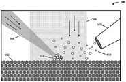
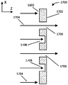
Fig. 4 and 5 are illustrative diagrams of one or more dual focus multi-beam systems 100 capable of simultaneously imaging and processing a sample in accordance with the present invention. Fig. 4 shows an illustrative view of etching a sample 402 with a processing beam 404 while imaging the sample with an imaging beam 406. FIG. 4 shows an insufflation system 408 that introduces a gas 410 into a volume near the location where the processing beam 404 is incident on the sample 402, such that the processing beam 404 causes a portion of the sample 402 to be removed.
FIG. 5 shows an illustrative view 504 of a processing beam used to perform gas-assisted deposition on a sample 502 and an imaging beam 506 while simultaneously imaging the sample 502. Fig. 5 shows an air injection system 508 that introduces a gas 510 into a volume near where the process beam 504 is incident on the sample 502, such that the process beam 504 causes an accumulation of physical deposits 512 (e.g., mounds, ridges, bridges, needles, etc.) on the sample 502.
Fig. 6 is a graphical representation of the optical performance of the bifocal multibeam system 100 according to the present invention. In particular, fig. 6 shows an example beam path of a bifocal multi-beam charged particle system 600 in which at least one quadrupole lens effect is applied to a non-axial imaging beam 602 and an axial processing beam 604.
Fig. 6 depicts an electron source 106 emitting a plurality of electrons 108 toward a dual-focus beam shaper 112. The dual-focus beamformer 112 is shown separating the plurality of electrons 108 into both a non-axial imaging beam 602 and a processing beam 604. Fig. 6 further illustrates the dual-focus beamformer 112 applying at least one quadrupole lens effect to the non-axial imaging beam 602, which changes the focusing characteristics of the non-axial imaging beam 602.
In some embodiments, the result of the quadrupole lens effect is that the non-axial imaging beam 602 is no longer a cylindrically symmetric beam. The multipole element 124 (e.g., multipole, stigmator, etc.) used to correct one or more astigmatisms and/or to make the non-cylindrically symmetric non-axial imaging beam 602 cylindrically symmetric is shown in fig. 6 as being positioned at the focal plane of the axial imaging beam 602. For example, the multipole element 124 can apply at least one quadrupole lens effect to the non-axial imaging beam 602 such that the non-axial imaging beam becomes cylindrically symmetric downstream of the multipole element 124. Because the corrector is positioned in the plane in which the axial processing beam 604 is focused to a point, the effect of the corrector on the beam is minimized. In addition, FIG. 6 shows an embodiment in which the multipole element 124 is further configured to apply an electromagnetic field (e.g., a dipole field) that applies a deflection to the beam perpendicular to the transmit axis. In FIG. 6, this deflection causes the non-axial imaging beam 602 to become an axial beam downstream of the multipole element 124 and the axial processing beam 604 to become a non-axial beam downstream of the multipole element 124.
The focusing column 126 is shown as containing a plurality of lateral lenses. The focusing column 126 is shown focusing the non-axial imaging beam 602 such that the TE imaging beam 602 is substantially parallel (or a slightly converging or diverging beam in the case of non-parallel TEM imaging) when the imaging beam 602 is incident on the sample 506. Fig. 6 further shows a focusing column 126 that focuses the processing beam 604 such that the processing beam has a focal plane at or near the sample plane. To illustrate this, fig. 6 depicts an inset 608 showing the focal plane of the processing beam 604 coinciding with the focal plane of the sample 606.
In the depicted embodiment, one of the multi-beam elements 124 and the dual-focus beam shaping mechanism 112 of the dual-focus multi-beam system 600 is further configured to apply dynamic deflection to the processing beam 604 such that the processing beam 604 scans the surface of the specimen 606, thereby causing a physical change to the specimen 606 (e.g., performing grinding, deposition, etching, contamination growth, charge conditioning, radiation damage, specimen deformation, heating, phase change, etc.). Because this dynamic deflection does not affect the imaging 602, the detector or detector array can simultaneously obtain detector data for imaging the sample as it is processed by the processing beam 604.
In addition, FIG. 6 shows a focusing column 126 that angles the processing beam 604 relative to the sample 606 such that the processing beam is blocked by the lower portion of the objective lens 610. In other embodiments, the processing beam 604 has an opposite angle to the sample 606, such that the processing beam is blocked by another type of beam blocker positioned below the sample.
Fig. 7 is an illustration of an example embodiment 700 of one or more bifocal multi-beam systems 100 for studying a specimen 104, wherein the bifocal beam shaper includes a MEMS device 702. One or more example dual focus multi-beam systems 700 include an electron source 106 that emits a plurality of electrons 108 along an emission axis 110 and toward an accelerator 120. The accelerator 120 accelerates/decelerates, focuses, and/or directs the first and second electron beams 114, 116 toward the dual focus beam shaper 112. Fig. 7 shows the accelerator 120 positioned upstream of the bifocal beamformer 112, as discussed above, in other embodiments, the bifocal beamformer 112 may be positioned between the electron source 106 and the accelerator 120.
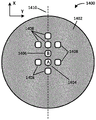
In one or more example dual focus multi-beam systems 700, the dual focus beamformer 112 corresponds to the MEMS device 702. The MEMS device 702 defines a first aperture and a second aperture, each configured to allow a portion of the plurality of electrons 108 to pass through the MEMS device 702. In this manner, the first and second apertures separate the plurality of electrons 108 into a first electron beam 114 and a second electron beam 116, respectively. Fig. 7 shows the first electron beam 114 as an axial beam.
The MEMS device 702 further includes a plurality of electrodes configured such that when certain voltages are applied thereto, the electrodes generate a quadrupole electromagnetic field that applies at least one quadrupole lens effect (i.e., dipole field, quadrupole field, hexapole field, octopole field, etc.) to the second electron beam 116. The quadrupole lens effect focuses, de-astigmatically, or otherwise modifies at least the second electron beam 116 such that corresponding focusing characteristics of the beams are different. In some embodiments, the electrodes are configured such that the first electron beam 114 is not affected and/or has reduced the effect of the electromagnetic field generated by the electrodes. Alternatively or additionally, a portion of the electrodes may generate an electromagnetic field that applies a different lensing effect to the first and second electron beams 114, 116.
Fig. 7 illustrates a MEMS device 702 positioned upstream of the focusing assembly 120, which is configured to apply a lens action that focuses at least one of the first and second electron beams 114, 116. In one or more example dual focus multi-beam systems 700 shown in fig. 7, the focusing assembly corresponds to a lens 120 that focuses and/or directs the first and second electron beams 114, 116 toward a focusing column 126. However, in other embodiments, the accelerator 122 may be positioned between the electron source 106 and the MEMS device 702, and the accelerator 122 may replace or augment the lens 704 (as shown in fig. 1).
The focusing column 126 and objective lens 128 focus the electron beams 114 and 116 so that they are incident on the sample 104. In particular, fig. 7 illustrates a focusing column 126 that focuses the second electron beam 116 to focus it on the sample 104 and the first electron beam 114 to focus it on the sample 104. Fig. 7 shows the second electron beam 116 as a reference beam passing through a thin portion of the sample 104 and the first electron beam 114 as a TEM beam incident on the sample 104.
In some embodiments, the focal planes of first and second electron beams 114, 116 are modified such that one of the beams is focused at a plane at or near sample 104 and the other electron beam is focused at a plane positioned at least 0.1%, 1%, 10%, or 100% above and/or below sample 104 by the focal length of the objective lens. Alternatively or additionally, the focal planes of the first and second electron beams 114, 116 may be modified such that one of the electron beams at the sample 104 has a diameter that is at least one of 5 times, 10 times, 20 times, 50 times, 100 times, 500 times, or 1000 times larger than the diameter of the other electron beam at the sample.
Fig. 8 shows a cross-section of an exemplary embodiment 800 of a MEMS device 700 according to the present invention. In particular, fig. 8 illustrates a cross-section of a MEMS device 700 configured to split a plurality of electrons 802 into a first electron beam 804 and a second electron beam 806 and to generate an electromagnetic field pattern that imparts at least one quadrupole lens effect to the second electron beam 806. The at least quadrupole lens effect causes the first electron beam 804 and the second electron beam 806 to have different focusing characteristics. For example, a quadrupole lens effect may impose a positive lens effect in one meridian plane (e.g., the y-z plane) and a negative lens effect in a perpendicular meridian plane (e.g., the x-z plane), thereby causing a different change in the focal properties of each of the two meridian planes. In such embodiments, another system component (e.g., a corrector or stigmator) may be included downstream of the dual-focus beamformer 700 to apply another quadrupole lens effect to again make the beam cylindrically symmetric.
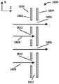
Fig. 8 shows a MEMS device 700 comprising a surface layer 808, an electrode layer 810, and an optional shielding layer 812. In fig. 8, the surface layer 808 is shown to comprise a thin material (e.g., foil) upon which the electrons 802 are incident. However, those skilled in the art will appreciate that in other embodiments, the surface layer 808 may not correspond to a separate component layer, but rather to the upper surface of one or more components of the MEMS device 700 upon which the electrons 802 are incident.
The surface layer 808 defines a first entrance 814 to a first diaphragm 816 and a second entrance 818 to a second diaphragm 820. In some embodiments, first stop 814 is an axial stop (i.e., positioned on the emission axis of electron 802) and second stop 818 is a non-axial stop. In such embodiments, the first electron beam 804 is an axial beam. The first entrance 814 allows a first portion of the electrons 802 (i.e., the first electron beam 804) to enter the first stop 816 and pass through the MEMS device 700. Similarly, the second entrance 818 allows a second portion of the electrons 402 (i.e., the second electron beam 806) to pass through the second stop 820 and through the MEMS device 700. The surface layer 808 inhibits the ability of the remainder of the electrons 802 to enter and/or pass through the MEMS device 700.
Fig. 8 also illustrates a MEMS device 700 that includes an optional shielding layer 812 opposite the surface layer 808 and configured to at least partially isolate the first electron beam 814 from at least the quadrupole lens effect applied to the second electron beam 816.
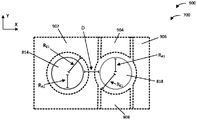
Fig. 9 shows a schematic top view of an example embodiment 900 of a MEMS device 700 comprising four electrodes. Fig. 9 and 10 illustrate in solid lines the first inlet 814 and the second inlet 818 as defined by the surface layer 808 in solid lines. In addition, fig. 9 and 10 show the components of the electrode layer 810 in dashed lines. Those skilled in the art will recognize that the dashed lines do not represent an exact shape, but rather indicate a generally contoured electrode in the electrode layer 810.
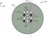
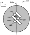
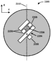
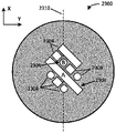
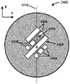
FIG. 9 illustrates a radius R of the first inlet 814A1The radius is less than or equal toRadius R of the first diaphragm defined at least in part by electrode 902E1. In an embodiment of the example MEMS device 900, the radius RA1May be 10 μm or so and the radius RE1And may be about 14 μm or greater. FIG. 9 illustrates the radius R of the second inlet 818A2A radius less than a radius R of a second diaphragm as defined at least in part by electrodes 902, 904, 906, and 908E2. However, in other embodiments, the radius RE1And a radius RA1And/or radius RE2And a radius RA2One or both of which may be the same. The example embodiment 900 is further illustrated as having equal and/or approximately equal radii RA1And a radius RA2However, this is not required for all embodiments. The first inlet 814 and the second inlet 818 are spaced apart by a distance D.
During use of the example MEMS device 900, a voltage may be applied to one or more of the electrodes 902-908 such that the electrodes generate an electromagnetic field that applies at least one quadrupole lens effect to the second electron beam. In some embodiments, one or more of the electrodes may be grounded. For example, when a first voltage V1 is applied to electrode 904 and a second voltage V2 is applied to electrode 908, the example MEMS device 900 can generate an electromagnetic field that applies at least one quadrupole lens effect to the second electron beam, and electrodes 902 and 906 are grounded. In various embodiments, V1 and V2 may each be greater than-20V and less than 20V, although greater voltages may also be used.
Fig. 10 shows a schematic top view of an example embodiment 1000 of a MEMS device 700 comprising seven electrodes. FIG. 10 illustrates the radius R of the first inlet 814A1A radius less than a radius R of the first diaphragm as defined at least in part by electrodes 1002, 1004, 1006, and 1008E1. Fig. 10 shows the first diaphragm 814 as an axial diaphragm through which the emission axis 1010 of the plurality of electrons passes.
FIG. 10 also shows the radius R of the second inlet 818A2A radius less than a radius R of a second diaphragm as defined at least in part by electrodes 1006, 1012, 1014, and 1016E2. However, in other embodiments, the radius RE1And a radius RA1And/or radius RE2And a radius RA2One or both of which may be the same.
During use of the example MEMS device 1000, voltages can be applied to one or more of the electrodes 1002-1008 and 1012-1016 such that the electrodes generate electromagnetic fields that apply at least one quadrupole lens effect to the second electron beam. In some embodiments, one or more of the electrodes may be grounded. For example, when a first set of voltages between values of-20V and 20V is applied to electrodes 1004, 1008, 1012, and 1016 and a second set of voltages between values of-5V and 5V is applied to electrodes 1002 and 1014, the example MEMS device 1000 may generate an electromagnetic field that applies at least one quadrupole lens effect to the second electron beam and electrode 1006 is grounded.
In addition, those skilled in the art will appreciate that the dashed lines in fig. 9 and 10 represent example configurations of electrodes, and that experiments will provide a plurality of electrode configurations (e.g., electrode sizes, electrode shapes, number of electrodes, electrode layouts, combinations of voltages applied to the electrodes, etc.) that will result in the electrodes generating electromagnetic fields that apply at least one quadrupole lens effect to the second electron beam. Further, although each of fig. 5 and 6 illustrate embodiments in which at least a quadrupole lens effect is applied to the second electron beam, in other embodiments, the electrode layers may be configured to generate an electromagnetic field that applies at least one quadrupole lens effect to the first electron beam (or both electron beams) when a corresponding set of voltages is applied to the electrodes.
FIG. 11 is an illustration 1100 of a change in the focusing characteristics of the second electron beam caused when the example embodiment dual-focus beam shaper causes at least one quadrupole lens effect to be applied thereto. In particular, fig. 11 shows an emitter 1102 that emits a plurality of electrons 1104 along an emission axis 1106. The plurality of electrons 1104 strike the dual-focus beam shaper 1108 in a circular region 1110. Fig. 11 shows the dual-focus beamformer 1108 as a MEMS device that (i) defines a first aperture 1112 and a second aperture 1114 that separate the electron beam 1104 into a first electron beam 1116 and a second electron beam 1118, respectively, and (ii) when in use generates an electromagnetic field that applies at least one quadrupole lens effect to the second electron beam 1118.
As illustrated in fig. 11, in some embodiments, at least one quadrupole lens effect causes the second electron beam 1118 to be distorted such that the second electron beam (i) has different focusing characteristics than the first electron beam 1116 and (ii) is no longer a cylindrically symmetric beam. In particular, fig. 11 shows the cross-sectional areas of the first electron beam 1116 and the second electron beam 1118 in a plane 1120 downstream of the dual focus beam shaper 1108, where the emission axis is perpendicular to the plane 1120. The first electron beam 1116 is shown as having a circular (or nearly circular) cross-section 1122 when the first electron beam 1116 crosses the plane 1120, and the second electron beam 1118 is shown as having a non-circular cross-section 1124 when the second electron beam 1118 crosses the plane 1120. The applicant notes that these cross sections do not illustrate the performance of all embodiments of the dual focus beam shaper according to the present invention, but are limited to a specific exemplary embodiment of the dual focus beam shaper 1108.
Fig. 12 is an illustration of an example embodiment 1200 of one or more bifocal multi-beam systems 100 for studying a specimen 104, wherein the bifocal beam shaper includes an array 1203 of diaphragm lenses.
One or more example dual focus multi-beam systems 1202 include an electron source 106 that emits a plurality of electrons 108 along an emission axis 110 and toward an array of diaphragm lenses 1204. The stop lens array 1204 includes at least one stop defining structure 1206 that defines: (i) a first aperture for allowing the first electron beam 114 to pass through the at least one aperture defining structure 1206; (ii) a second aperture for allowing the second electron beam 116 to pass through the at least one aperture defining structure 1206; and (iii) a plurality of other diaphragms. The first aperture, the second aperture, and the plurality of apertures collectively form a pattern that generates an electromagnetic field that imparts a lensing effect (e.g., at least one quadrupole lens effect) to at least one of the first electron beam 114 and the second electron beam 116 when one or more voltages are applied to the aperture defining structure 1206 and the one or more electrodes 1208. The lens effect distorts one or both of the first and second electron beams 114, 116 such that they have different focusing characteristics.
The stop lens array 1204 further includes one or more electrodes (e.g., disk-shaped electrodes) 1208. Each of the one or more electrodes 1208 generates an electric field between the corresponding electrode and the at least one aperture-defining structure 1206 when a voltage is supplied thereto. Additionally, in some embodiments, the one or more electrodes 1208 may physically block a portion of the plurality of electrons 108 from reaching the at least one diaphragm-defining structure 106. For example, one of the electrodes 1208 may define a first aperture that allows a first portion of the electrons (i.e., a first electron beam) to pass through the electrode and a second aperture that allows a second portion of the electrons (i.e., a second electron beam) to pass through the electrode.
Fig. 12 illustrates a dual-focus beam shaper 112 positioned upstream of a focusing assembly 120 configured to apply a lens action that focuses at least one of a first electron beam 114 and a second electron beam 116. In one or more example dual focus multi-beam systems 1202 shown in fig. 12, the focusing assembly corresponds to the accelerator 122 accelerating/decelerating, focusing, and/or directing the first and second electron beams 114, 116 toward the focusing column 126.
The focusing column 126 and objective lens 128 focus the electron beams 114 and 116 so that they are incident on the sample 104. In particular, fig. 12 illustrates a focusing column 126 that focuses the second electron beam 116 to a plane at or near the sample 104 and the first electron beam 114 to a plane at or near the sample 104. In some embodiments, the focusing characteristics of first and second electron beams 114, 116 are modified such that one of the beams is focused at a plane at or near sample 104 and the other electron beam is focused at a plane positioned at least 0.1%, 1%, 10%, or 100% above and/or below sample 104 by the focal length of the objective lens. Alternatively or additionally, the focusing characteristics of the first and second electron beams 114, 116 may be modified such that one of the electron beams at the sample 104 has a diameter that is at least one of 50 times, 100 times, 500 times, or 1000 times larger than the diameter of the other electron beam at the sample.
Fig. 13 illustrates an example 1300 electrode 1202 of an example stop lens array 1204. Fig. 13 shows the electrode 1208 as a disc-shaped electrode 1302 defining a diaphragm 1304 that allows electrons to pass through the disc-shaped electrode 1302.
Fig. 14 illustrates an example 1400 diaphragm defining structure 1402 of an example diaphragm lens array 1204. The example stop defining structure 1402 defines: (i) a first diaphragm 1404 for allowing a first electron beam to pass through the at least one diaphragm defining structure 1402; (ii) a second aperture 1406 for allowing a second electron beam to pass through the at least one aperture defining structure 1402; and (iii) a plurality of other diaphragms 1408. In the example embodiment shown in fig. 14, each of the first aperture 1404, the second aperture 1406, and the three apertures 1408 are positioned along a midline 1410 of the aperture-defining structure 1402.
Fig. 14 shows each of the plurality of other apertures 1408 as an aperture that allows electrons to pass through the aperture defining structure 1402. However, in other embodiments, one or more of the apertures 1408 may be a cavity in which the aperture defining structures 1402 define empty spaces into which electrons are allowed, but do not allow electrons to pass through the aperture defining structures. The first aperture 1404, the second aperture 1406, and the plurality of apertures 1408 collectively form a pattern that induces an electromagnetic field that imparts a lens effect (e.g., at least one quadrupole lens effect) to at least the second electron beam.
FIG. 15 illustrates a cross-section of an example stop lens array 1500 having one stop defining structure. In particular, fig. 15 shows a cross-section of an example diaphragm lens array 1500 including the example electrode 1302 of fig. 13 and the example diaphragm structure 1402 of fig. 14, wherein a cut of the cross-section is aligned with a midline 1410 of the example diaphragm structure 1402.
Fig. 15 shows electrons 1502 emitted along an emission axis toward electrode 1302. A portion of the electrons 1502 passes through both the stop 1304 and the first stop 1404, becoming a first electron beam 1506. Another portion of the electrons 1502 passes through both the aperture 1304 and the second aperture 1406, becoming a second electron beam 1508. In some embodiments, the stop lens array 1500 includes a second electrode positioned such that the at least one stop defining structure 1402 is interposed between the two electrodes. When a voltage is applied to the electrode 1302 (a), the electrode 1302 (B), both electrodes 1302 (a) and 1302 (B), and/or the aperture defining structure 1402, an electromagnetic field is generated between the electrode 1302 and the aperture defining structure 1402. Although fig. 15 illustrates the stop lens array 1500 including two electrodes, in some embodiments, the stop lens array 1500 may include only one electrode (electrode 1302 (a) or 1302 (B)).
The aperture lens array 1500 is configured such that the configuration of the electrodes 1302 (i.e., one electrode, two electrodes, the position of such electrodes, the geometry of such electrodes, etc.), the voltages (or lack thereof) applied to the individual ones of the electrodes 1302 and the aperture defining structure 1402, and the pattern formed collectively by the first aperture 1404, the second aperture 1406, and the plurality of apertures 1408, generate an electromagnetic field that produces a first lens effect on the first electron beam and a second lens effect on the second electron beam, wherein the first lens effect and the second lens effect are different. For example, in embodiments of the present invention, the electromagnetic field may produce a lens effect (e.g., at least one quadrupole lens effect) that causes the first and second electron beams 1506, 1508 to have different focusing characteristics.
In some embodiments, the electromagnetic field also offsets one or both of the first and second electron beams 1506, 1508 from the emission axis 1504. Moreover, although fig. 15 illustrates the first electron beam 1508 as an axial beam traveling along emission axes 1504 of the plurality of electrons 1502, this is not required in all embodiments.
Fig. 16-24 illustrate example central structures that may be used in the multi-stop assembly 2500 illustrated in fig. 25. In particular, fig. 16 illustrates an example diaphragm defining structure 1600 of an example diaphragm lens array comprising a combination of apertures and cavities. The example diaphragm defining structure 1602 defines: (i) a first aperture 1604 that allows a first electron beam to pass through the at least one aperture defining structure 1602; (ii) a second diaphragm 1606 for allowing the second electron beam to pass through the at least one diaphragm defining structure 1602; and (iii) a plurality of other diaphragms 1608. When a voltage is applied to at least the diaphragm defining structure 1600 and the electrodes 2504 and 2512 during use of the multi-diaphragm assembly 2500, the first diaphragm 1604, the second diaphragm 1606 and the plurality of diaphragms 1608 collectively form a mode that induces an electromagnetic field that imparts a lens effect (e.g., at least one quadrupole lens effect) to at least the second electron beam. In some embodiments, the stop lens structure 1602 includes a single physical component that defines the first stop 1604, the second stop 1606 and each of the plurality of stops 1608. However, in other embodiments, the stop lens structure 1602 may include two or more component physical structures.
Fig. 16 illustrates an example embodiment, where five of the plurality of other apertures 1608 correspond to apertures 1610, and four of the plurality of other apertures 1608 correspond to cavities 1612. However, in other embodiments, the plurality of other apertures 1608 may include other combinations and/or patterns of apertures and cavities, including embodiments in which all of the plurality of other apertures 1608 exclusively correspond to one of the apertures (e.g., the aperture-defining structure shown in fig. 14) or cavities. In the example embodiment shown in fig. 16, each of the first diaphragm 1604, the second diaphragm 1606 and the two other diaphragms 1608 are positioned along a line 1614 of the diaphragm defining structure 1602.
Fig. 17 illustrates a cross-section 1700 of an example diaphragm structure 1602, which includes a single physical structure 1702. In particular, fig. 17 shows a cross-section of an embodiment of the example diaphragm structure 1602 of fig. 16, where the cut-out of the cross-section is aligned with the line 1614. A first portion of electrons 1704 are allowed to pass through physical structure 1702 through aperture 1706. FIG. 17 further shows that a second portion of electrons 1704 are allowed to enter cavity 1708, which prevents them from passing through physical structure 1702.
Fig. 18 illustrates a cross-section 1800 of an example diaphragm structure 1602, which includes a first physical structure 1802 and a second physical structure 1804. In particular, fig. 18 shows a cross-section of an embodiment of an example diaphragm structure 1602, where the example diaphragm structure includes two structures (e.g., foils) with cuts of the cross-section aligned with lines 1614. Fig. 18 illustrates an aperture 1806 in an example diaphragm structure 1602 corresponding to complementary diaphragms in a first physical structure 1802 and a second physical structure 1804 that together allow a first portion of an electron 1808 to pass through the diaphragm structure 1602. Fig. 18 also shows a cavity 1810 corresponding to the stop in the first physical structure 1802 that does not have a complementary stop in the second physical structure 1804. In other words, the cavity 1810 is configured such that a second portion of the electrons 1808 are allowed to enter the space 1812 between the first physical structure 1802 and the second physical structure 1804, but are not allowed to pass through the diaphragm structure 1602.
Fig. 19 and 20 illustrate a pair of component physical structures that may be used to form the aperture defining structure 2306 in the aperture lens array 2500 illustrated in fig. 25. In particular, fig. 19 illustrates an example first component physical structure 1900 of an example diaphragm defining structure that includes two physical structures. The example first component physical structure 1900 defines: (i) a first stop 1904 that allows the first electron beam to pass through first assembly physical structure 1900; (ii) a second stop 1906 that allows the second electron beam to pass through the first assembly physical structure 1900; and (iii) a plurality of other diaphragms 1908. Each of these diaphragms is illustrated as having a rectangular geometry (e.g., an elongated slot). Such rectangular apertures are configured to produce a cylindrical lens effect on electrons passing through them during use of the example aperture-defining structure. In the example embodiment shown in fig. 19, each of the first stop 1904, the second stop 1906, and the two stops 1908 are positioned along a midline 1910 of the first component physical structure 1900.
Fig. 20 illustrates an example second component physical structure 2000 of an example diaphragm defining structure comprising two physical structures. Example second component physical structure 2000 defines: (i) a first aperture 2004 that allows the first electron beam to pass through the second assembly physical structure 2000; (ii) a second aperture 2006 that allows the second electron beam to pass through the second assembly physical structure 2000; and (iii) a plurality of other diaphragms 2008. Diaphragms 2004 and 2008 are shown having a rectangular geometry, similar to the diaphragms defined by the first assembly physical structure 1900 illustrated in FIG. 19. The second diaphragm 2006 is shown in fig. 20 as combining both rectangular and circular geometries. In other words, the second diaphragm 2006 is shown as a circular diaphragm positioned in the center and covered by a diaphragm having a rectangular geometry. This combination of the geometries of the second stop 1906 and the second stop 2006 is such that a net quadrupole lens effect is applied to the electron beam B as it passes through the second stops 1906 and 2006. Similarly, the geometry of the first stop 1904 and the first stop 2004 is such that no net lens effect is applied to the electron beam a. In the example embodiment shown in fig. 20, first diaphragm 2004, second diaphragm 2006, and each of the two diaphragms 2008 are positioned along a midline 2010.
Fig. 21 and 20 illustrate a pair of component physical structures that may be used to form the aperture defining structure 2306 in the aperture lens array 2500 illustrated in fig. 25. In particular, fig. 21 illustrates an example first component physical structure 2100 of an example diaphragm defining structure that includes two physical structures. The example first component physical structure 2100 defines: (i) a first aperture 2104 that allows the first electron beam to pass through the first assembly physical structure 2100; (ii) a second stop 2106 that allows the second electron beam to pass through the first assembly physical structure 2100; and (iii) a plurality of other diaphragms 2108. Such apertures are configured to produce a quadrupole lens effect on electrons passing through the second aperture 2106 during use of the example aperture defining structure. In the example embodiment shown in fig. 21, each of the first stop 2104, the second stop 2106 and the other stops 2108 are positioned along a midline 2110 of the first component physical structure 2100.
Fig. 22 illustrates an example second component physical structure 2200 of an example stop defining structure comprising two physical structures. The example second component physical structure 2200 defines: (i) a first aperture 2204 that allows the first electron beam to pass through the second assembly physical structure 2200; (ii) a second aperture 2206 that allows the second electron beam to pass through the second assembly physical structure 2200; and (iii) a plurality of other diaphragms 2208. Diaphragms 2204 and 2208 are shown having geometric shapes similar to those defined by the first component physical structure 2200 illustrated in fig. 22. The combination of the geometry of the second stop 2106 and the second stop 2206 is such that no net lens effect is applied to the electron beam a. Similarly, the geometry of the first aperture 2104 and the first aperture 2204 is such that a net quadrupole lens effect is applied to the electron beam B as it passes through the second apertures 2106 and 2206. In the example embodiment shown in fig. 22, each of first stop 2204, second stop 2206, and two stops 2028 are positioned along a centerline 2210.
Fig. 23 and 24 illustrate a pair of component physical structures that may be used to form the aperture defining structure 2506 in the aperture lens array 2500 illustrated in fig. 25. In particular, fig. 23 illustrates an example first component physical structure 2300 of an example diaphragm defining structure comprising two physical structures. The example first component physical structure 2300 defines: (i) a first aperture 2304 that allows the first electron beam to pass through the first assembly physical structure 2300; (ii) a second aperture 2306 for allowing a second electron beam to pass through the first assembly physical structure 2300; and (iii) a plurality of other apertures 2308. Each of these diaphragms is illustrated as having a rectangular geometry (e.g., an elongated slot). Such rectangular apertures are configured to produce a cylindrical lens effect on electrons passing through them during use of the example aperture-defining structure. In the example embodiment shown in fig. 23, each of the first diaphragm 2304, the second diaphragm 2306, and the two diaphragms 2308 are positioned along a midline 2310 of the first component physical structure 2300.
Fig. 24 illustrates an example second component physical structure 2400 of an example diaphragm defining structure that includes two physical structures. Example second component physical structure 2400 defines: (i) a first stop 2404 that allows the first electron beam to pass through the second assembly physical structure 2400; (ii) a second stop 2406 that allows the second electron beam to pass through the second assembly physical structure 2400; and (iii) a plurality of other diaphragms 2408. Diaphragms 2404 and 2408 are shown having a rectangular shape, similar to the diaphragms defined by the first assembly physical structure 2300 illustrated in FIG. 23. This combination of the geometry of the second aperture 2306 and the second aperture 2406 is such that no net lens effect is applied to the electron beam a. Similarly, the geometry of the first aperture 2304 and the first aperture 2404 is such that a net quadrupole lens effect is applied to the electron beam B as it passes through the second apertures 2306 and 2406. In the example embodiment shown in fig. 24, first stop 2404, second stop 2406, and each of the two stops 2408 are positioned along a centerline 2410.
Fig. 25 illustrates a cross-section of an example stop lens array 2500 that includes a first electrode 2502, a second electrode 2504, and a stop defining structure 2506. Fig. 25 shows electrons 2508 emitted toward the first electrode 2502. The first electrode 2502 is shown as defining a pair of stops 2512 that allow a portion of the electrons 2508 to pass through the first electrode 2502. In some embodiments, the first electrode 2502 may correspond to a conductive foil defining two diaphragms 2512. A first portion of the electrons 2508 pass through a first stop and become a first electron beam 2514. Another portion of the electrons 2508 pass through a second stop, becoming a second electron beam 2516.
In all embodiments, the stop lens array 2500 includes a second electrode 2504 positioned such that the stop defining structure 2506 is interposed between the two electrodes. The second electrode 2504 may correspond to a disk-shaped electrode defining a diaphragm 2518 that allows the first and second electron beams 2514 and 2516 to pass through the second electrode 2504.
When a voltage is applied to both electrodes 2502 and 2504 and/or the aperture defining structure 2506, an electromagnetic field is generated between the electrodes 2502 and 2504. The electromagnetic field and the pattern of the stop defined by the stop defining structure 2506 collectively produce a lens effect that causes the first and second electron beams 2514 and 2516 to have different focal planes.
Although non-limiting, a simple representative calculation may be used to demonstrate the performance of some embodiments of the invention with different array patterns for upstream and downstream components (e.g., the embodiment depicted in fig. 19 and 20, the embodiment depicted in fig. 21 and 22, the embodiment depicted in fig. 23 and 24). To achieve this simple representative calculation, the following paragraphs assume (a) Everywhere (b) above the aperture-defining
 structure 2306, near the field component of the aperture array plate From
From (i.e., a non-zero light field above the aperture defining structure 2506) becomes 0, (c) a field component below the
 aperture defining structure 2506, near the aperture array plate From 0 to
 (i.e., a non-zero light field under the stop-defining structure 2506), and (d) the field between the array plates is zero field (e.g., the plates in fig. 19 and 20).
In a simple representative calculation, the electrostatic potential of up to 2 orders in the x and y directions can be generally expressed as:

for electrostatic potentials that are mirror symmetric in the x-z plane and the y-z plane. In the expression (1) given above, the expression,Urepresenting electron energy above the aperture lens array 2500, and other terms are caused by voltages applied to both the electrode 2502 and the electrode 2504 and/or the aperture defining structure 2506. Laplace equation of the electrostatic potential (Laplace equation) ((L)) ) Indication of
 . In some examples, for a circular stop lens, this corresponds to
 And for a cylindrical lens focused in the x-z plane (as in the embodiment depicted in fig. 19), this corresponds to
 And isq = 0。
According to a simple representative calculation, the upstream components of the stop-defining structure 2506 excite the lens intensity:
similarly, downstream components of the stop-defining structure 2506 excite lens intensities:
in the context of these equations, the equation, and
and are focal lengths in the x-z plane and the y-z plane, respectively, and
 and
and is formed by quadrupole potentials
 Induced quadrupole lens strength.
In some of the preferred embodiments of the present invention, . In such embodiments, the total lens strength is reduced to:
because of the fact that Therefore, it is found in such embodiments
 This means that only a pure quadrupole lens action is present.
In an embodiment of the stop-lens array 2100, where the electromagnetic fields on both sides of the physical structures 1900 and 2000 are the same, the lens effect caused by the first electron beam 2108 traveling through the first stop 1904 is cancelled and/or otherwise eliminated by the lens effect caused by the first electron beam 2108 traveling through the first stop 2004. Additionally, in this embodiment, the lens effect caused by the second electron beam 2110 traveling through the second aperture 1906 and the lens effect caused by the second electron beam 2110 traveling through the second aperture 2006 are combined to form at least one quadrupole lens effect.
Fig. 26 is an illustration of an example embodiment 2600 of one or more bifocal multi-beam electronic systems 100 for studying a sample 104, wherein the bifocal beam shaper 112 includes a beam splitting mechanism 2604 and one or more focusing devices 2606.
One or more example dual-focus multi-beam electronic systems 2602 include an electron source 106 that emits a plurality of electrons 108 along an emission axis 110 and toward a dual-focus beam shaper 112. In the illustrated embodiment of the invention, the dual-focus beam shaper 112 is shown to include at least (i) a beam splitting mechanism 2604 that splits the plurality of electrons 108 into the first and second electron beams 114, 116, and (ii) one or more focusing devices 2606 configured to modify the focusing characteristics of one or both of the electron beams such that the two beams do not have the same corresponding focal plane. In some embodiments, the one or more focusing devices 2606 are further configured to deflect one or both of the first electron beam 114 and the second electron beam 116 away from the emission axis 110.
In fig. 26, the beam splitting mechanism 2604 is shown to correspond to a physical structure defining a first aperture that allows the first electron beam 114 to pass through the beam splitting mechanism 2604 and a second aperture that allows the second electron beam 116 to pass through the beam splitting mechanism 2604. Fig. 26 further illustrates one or more focusing devices 2606, optionally corresponding to two lenses. However, in other embodiments, the focusing device 2606 may correspond to three or more lenses, a single lens that modifies only one of the electron beams, a single lens with high aberrations such that both electron beams pass through the lens. Additionally, although fig. 26 illustrates the beam splitting mechanism 2604 upstream of the one or more focusing devices 2606, in other embodiments of the example bifocal multi-beam electronic system 2602, the beam splitting mechanism 2604 may be downstream of the one or more focusing devices 2606. Alternatively, in some embodiments, some of the focusing devices 2606 may be located upstream of the beam splitting mechanism 2604, while others of the focusing devices 2606 may be located downstream of the beam splitting mechanism 2604.
Fig. 26 illustrates a dual-focus beam shaper 112 positioned upstream of a focusing assembly 120 configured to apply a lens action that focuses at least one of a first electron beam 114 and a second electron beam 116. In one or more example dual focus multi-beam electronic systems 2602 shown in fig. 26, the focusing assembly corresponds to the accelerator 122 that accelerates/decelerates, focuses, and/or directs the first and second electron beams 114, 116 toward the focusing column 126.
The focusing column 126 and objective lens 128 focus the electron beams 114 and 116 so that they are incident on the sample 104. In particular, fig. 26 illustrates a focusing column 126 that focuses the second electron beam 116 to focus it on the sample 104 and the first electron beam 114 to focus it on the sample 104. In some embodiments, the focal planes of first and second electron beams 114, 116 are modified such that one of the beams is focused at a plane at or near sample 104 and the other electron beam is focused at a plane positioned at least 0.1%, 1%, 10%, or 100% above or below sample 104 by the focal length of the objective lens. Alternatively or additionally, the focal planes of the first and second electron beams 114, 116 may be modified such that one of the electron beams at the sample 104 has a diameter that is at least one of 50 times, 100 times, 500 times, or 1000 times larger than the diameter of the other electron beam at the sample.
Examples of inventive subject matter according to the present disclosure are described in the paragraphs listed below.
A1. A method for investigating a sample, the method comprising emitting a plurality of charged particles towards the sample; forming the plurality of charged particles into a first charged particle beam and a second charged particle beam; modifying a focusing characteristic of at least one of the first charged particle beam and the second charged particle beam.
A1.1. The method of paragraph a1, wherein modifying the focusing characteristics of at least one of the first and second charged particle beams includes modifying one or more of the first and second charged particle beams such that: the first charged particle beam has a first focal plane; and the second charged particle beam has a second focal plane different from the first focal plane.
A1.1.1. The method of paragraph a1.1, wherein modifying the focusing characteristics of at least one of the first and second charged particle beams comprises modifying one or more of the first and second charged particle beams such that: the first charged particle beam has a focal plane at a plane at or near the sample; and the second charged particle beam does not have a focal plane at the plane at or near the sample.
A1.1.2. The method of paragraph a1.1, wherein modifying the focusing characteristics of at least one of the first and second charged particle beams comprises modifying one or more of the first and second charged particle beams such that: the second charged particle beam has a focal plane at a plane at or near the sample; and the first charged particle beam does not have a focal plane at the plane at or near the sample.
A1.2. The method of any of paragraphs a1-A1.1.2, wherein modifying the focusing characteristics of at least one of the first charged particle beam and the second charged particle beam comprises applying a circular lens action to one of the first charged particle beam and the second charged particle beam.
A1.2.1. The method according to paragraph a1.2, wherein modifying the focusing characteristics of at least one of the first and second charged particle beams comprises applying the circular lens action to both of the first and second charged particle beams.
A1.2.1.1. The method of paragraph A1.2.1, wherein the circular lensing applied to the first charged particle beam is different than the circular lensing applied to the second charged particle beam.
A1.3. The method of any of paragraphs a1-A1.2.1.1, wherein modifying the focusing characteristics of at least one of the first charged particle beam and the second charged particle beam comprises applying at least one quadrupole lens action to one of the first charged particle beam and the second charged particle beam.
A1.4. The method of any of paragraphs A1-a1.3, wherein the first charged particle beam is an axial beam traveling along an emission axis of the plurality of charged particles and the second charged particle beam is a non-axial beam.
A1.5. The method of any of paragraphs A1-a1.4, wherein the second charged particle beam is an axial beam traveling along an emission axis of the plurality of charged particles, and the first charged particle beam is a non-axial beam.
A2. The method of any of paragraphs A1-a1.5, wherein the charged particles are electrons and the beam of charged particles is an electron beam.
A3. The method of any of paragraphs a1-a2, wherein a second beam diameter of the second charged particle beam at the sample is at least one of 5 times, 10 times, 20 times, 50 times, 100 times, 500 times, or 1000 times larger than a first beam diameter of the first charged particle beam at the sample.
A3.1. The method of paragraph a3, wherein the second beam diameter is at least one of 5 times, 10 times, 20 times, 50 times, 100 times, 500 times, or 1000 times larger than the first beam diameter at or near each intersection of the first charged particle beam.
A4. The method of any of paragraphs a1-a3.1, wherein the first charged particle beam is tilted with respect to the second charged particle beam at the sample.
A5. The method of any of paragraphs a1-a4, wherein the first charged particle beam and the second charged particle beam are coherent beams.
A6. The method of any of paragraphs a1-a5, further comprising accelerating each of the first and second charged particle beams to a final energy with an accelerator.
A7. The method of any of paragraphs a1-a5, further comprising accelerating the plurality of charged particles to a final energy with an accelerator.
A8. The method of any of paragraphs a1-a7, wherein each of the forming the plurality of charged particles and the modifying the focusing characteristics is performed by a dual-focus beam shaper.
A8.1. The method of paragraph A8 when dependent on a6, wherein the dual focus beamformer is positioned over an accelerator.
A8.2. The method of paragraph A8 when dependent on a7, wherein the dual focus beamformer is positioned below an accelerator.
A8.3. The method of any of paragraphs A8-a8.2, wherein the dual focus beam shaper distorts the second charged particle beam.
A8.4. The method of any of paragraphs A8-a8.3, wherein the dual focus beam shaper changes the focal plane of the second charged particle beam.
A8.5. The method of any of paragraphs A8-a8.4, wherein the dual focus beam shaper causes the second charged particle beam not to be a cylindrically symmetric beam.
A8.5.1. The method of paragraph a8.5, further comprising making the second charged particle beam a cylindrically symmetric beam with an stigmator.
A8.6. The method of any one of A8-A8.5.1, wherein the dual focus beam shaper imparts one or more aberrations to the second charged particle beam.
A8.6.1. The method of paragraph a8.6, wherein at least one of the one or more aberrations is a deterministic aberration.
A8.6.2. The method of any of paragraphs a8.6-8.6.1, wherein the dual-focus beamformer is positioned and/or configured to cause at least one of the one or more aberrations to correct another aberration in the system.
A8.7. The method of any of paragraphs A8-A8.6.2, wherein the dual-focus beam shaper is further configured to deflect at least one of the first charged particle beam and the second charged particle beam away from an emission axis of the plurality of charged particles.
A9. The method according to any of paragraphs A8-a8.7, wherein the dual-focus beam shaper comprises a MEMS device configured to produce at least one quadrupole lens effect that causes, at least in part, the modifying of the focusing characteristics of at least one of the first and second charged particle beams.
A9.1. The method of paragraph a9, wherein the MEMS device includes a structure defining a first aperture and a second aperture, and wherein the first charged particle beam passes through the first aperture and the second charged particle beam passes through the second aperture.
A9.1.1. The method of paragraph a9.1, wherein the first stop has the same radius as the second stop.
A9.1.2. The method of paragraph a9.1, wherein the first stop has a smaller radius than the second stop.
A9.1.3. The method of paragraph a9.1, wherein the first stop has a larger radius than the second stop.
A9.1.4. The method of any of paragraphs a9.1-A9.1.3, wherein the MEMS device comprises a surface layer facing the plurality of charged particles, and wherein the first and second optical stops are defined by the surface layer.
A9.1.4.1. The method of paragraph A9.1.4, wherein the surface layer is a foil.
A9.1.5. The method of any of paragraphs a9.1-A9.1.4.1, wherein the first diaphragm is an axial diaphragm positioned on an emission axis of the plurality of charged particles and the second diaphragm is a non-axial diaphragm.
A9.1.6. The method of any of paragraphs a9.1-A9.1.4.1, wherein the second diaphragm is an axial diaphragm positioned on an emission axis of the plurality of charged particles, and the first diaphragm is a non-axial diaphragm.
A9.2. The method of any of paragraphs a9-A9.1.5, wherein the MEMS device comprises one or more electrodes.
A9.2.1. The method of paragraph a9.2, wherein the one or more electrodes generate an electromagnetic field that at least partially at least applies the quadrupole lens effect when a corresponding voltage is applied to the one or more electrodes.
A9.2.1. The method of any of paragraphs a9.2-A9.2.1, wherein at least one of the one or more electrodes is grounded.
A9.2.2. The method of any of paragraphs a9.2-A9.2.1 when dependent on A9.1.4, wherein the MEMS device comprises an insulating layer opposite the surface layer.
A9.2.2.1. The method of paragraph A9.2.2, wherein the one or more electrodes are located in an electrode layer positioned between the insulating layer and the surface layer.
A9.2.3. The method of any of paragraphs a9.2-A9.2.2.1, wherein the one or more electrodes comprise four electrodes.
A9.2.4. The method of any of paragraphs a9.2-A9.2.2.1, wherein the one or more electrodes comprise seven electrodes.
A9.3. The method of any of paragraphs a9-A9.2.4, wherein the at least quadrupole lens effect is one of a dipole lens effect, a quadrupole lens effect, a hexapole lens effect, and an octopole lens effect.
A9.4. The method according to any of paragraphs A9-a9.3, wherein at least a quadrupole field does not change the focal plane of the first charged particle beam.
A9.5. The method of any of paragraphs A9-a9.4, wherein the MEMS device is further configured to generate one or more dipole fields.
A9.5.1. The method of paragraph a9.5, wherein the one or more dipole fields deflect at least one of the charged particle beams in a direction perpendicular to the emission axis.
A9.6. The method of any of paragraphs a9-A9.5.1, wherein the quadrupole lens effect: applying a positive lens effect to the first charged particle beam in a first meridional plane of the first charged particle beam; and applying a negative lens effect to the first charged particle beam in a second meridional plane of the first charged particle beam, wherein the first meridional plane is perpendicular to the second meridional plane.
A9.6.1. The method of paragraph a9.6, wherein a first change in the focal plane of the first charged particle beam caused by the quadrupole field in the first meridional plane is different from a second change in the focal plane of the first charged particle beam caused by the quadrupole field in the second meridional plane.
A9.7. The method of any of paragraphs a9-A9.5.1, wherein the quadrupole lens effect: applying a positive lens effect to the second charged particle beam in a first meridian plane of the second charged particle beam; and applying a negative lens effect to the second charged particle beam in a second meridional plane of the second charged particle beam, wherein the first meridional plane is perpendicular to the second meridional plane.
A9.7.1. The method of paragraph a9.7, wherein a first change in the first meridional plane of the focal plane of the second charged particle beam caused by the quadrupole field is different from a second change in the second meridional plane of the focal plane of the second charged particle beam caused by the quadrupole field.
A10. The method of any of paragraphs A8-A8.6.2, wherein the dual focus beam shaper comprises: a physical structure defining a first aperture and a second aperture, wherein the first charged particle beam passes through the first aperture and the second charged particle beam passes through the second aperture; and a lens positioned and/or configured to adjust the focusing characteristics of at least one of the first and second charged particle beams such that the charged particle beams have different corresponding focal planes.
A10.1. The method of paragraph a10, wherein the first charged particle beam passes through the first diaphragm and the second charged particle beam passes through the second diaphragm.
A10.2. The method of any of paragraphs a10-a10.1, wherein the lens is a singlet lens.
A10.3. The method of any of paragraphs a10-a10.2, wherein the lens is positioned over the physical structure.
A10.4. The method of any of paragraphs a10-a10.2, wherein the lens is positioned above and below the physical structure.
A10.5. The method of any of paragraphs a10-a10.4, wherein the lens is positioned and/or configured to adjust the focusing characteristics of the second charged particle beam.
A10.5.1. The method of paragraph a10.5, wherein the lens is not positioned and/or configured to adjust the focal plane of the first charged particle beam.
A11. The method according to any of paragraphs A6-a6.5, wherein the dual focus beam shaper comprises at least one physical structure defining: a first aperture that allows the first charged particle beam to pass through the at least one physical structure; a second aperture for allowing the second charged particle beam to pass through the at least one physical structure; and a plurality of other diaphragms.
A11.1. The method of paragraph a11, wherein the first aperture, the second aperture and the plurality of other apertures form a pattern that creates an electromagnetic field that imparts a lens effect on the second charged particle beam during use of the dual focus beam shaper.
A11.1.1. The method of paragraph a11.1, wherein the first aperture, the second aperture and the plurality of further apertures form a pattern that produces an electromagnetic field that applies at least one quadrupole lens effect to the second charged particle beam during use of the dual focus beam shaper.
A11.1.1.1. The method of paragraph A11.1.1, wherein the electromagnetic field does not apply the quadrupole lens effect to the first charged particle beam during use of the dual-focus beamformer.
A11.1.2. The method of any of paragraphs a11.1-A11.1.1.1, wherein the first diaphragm, the second diaphragm, and the plurality of other diaphragms form a pattern that generates an electromagnetic field that imparts a circular lens effect on the first charged particle beam during use of the dual focus beamformer.
A11.1.2.1. The method of paragraph A11.1.2, wherein the plurality of other apertures form a pattern that creates an electromagnetic field that imparts at least one circular lens effect to the second charged particle beam during use of the dual focus beam shaper.
A11.1.3. The method of any of paragraphs a11.1-A11.2.1, wherein the lens effect applied by the electromagnetic field at least partially causes the modifying of the focusing characteristic of at least one of the first charged particle beam and the second charged particle beam.
A11.1.3.1. The method of paragraph A11.1.3, wherein the electromagnetic field does change the focal plane of the first charged particle beam.
A11.3. The method of any of paragraphs a11-A11.2.1, wherein at least one diaphragm of the plurality of diaphragms is an aperture.
A11.3.1. The method of paragraph a11.3, wherein the aperture comprises:
an inlet defined in a first surface of the at least one physical structure, the first surface facing the plurality of charged particles; an outlet defined in a second surface of the at least one physical structure opposite the first surface; and an empty volume connecting the inlet and the outlet.
A11.3.1.1. The method of paragraph A11.3.1, wherein the first surface and the second surface are each surfaces of a single physical structure.
A11.3.1.2. The method of paragraph A11.3.1, wherein the first surface and the second surface are each surfaces of different physical structures.
A11.4. The method of any of paragraphs a11-A11.3.1.2, wherein at least one diaphragm of the plurality of diaphragms is a cavity.
A11.4.1. The method of paragraph a11.4, wherein the cavity comprises: an inlet defined in a first surface of the at least one physical structure, the first surface facing the plurality of charged particles; and a void volume in communication with the inlet and defined by the at least one physical structure, wherein the at least one physical structure defines the void volume such that charged particles of the plurality of charged particles entering the void volume through the inlet do not pass through the dual-focus beam shaper.
A11.4.1.1. The method of paragraph A11.4.1, wherein the cavity is defined by a single physical structure.
A11.4.1.2. The method of paragraph A11.4.1, wherein the cavity is defined by a plurality of physical structures.
A11.5. The method of any of paragraphs a11.3-A11.4.1.2, wherein the plurality of diaphragms comprises a combination of apertures and cavities.
A11.6. The method of any of paragraphs a11-a11.5, wherein a geometry of at least one of the first diaphragm, the second diaphragm, or the plurality of diaphragms is circular.
A11.7. The method of any of paragraphs a11-a11.5, wherein a geometry of at least one of the first diaphragm, the second diaphragm, or the plurality of diaphragms is rectangular.
A11.7.1. The method of any of paragraphs a11-a11.5, wherein the geometry of at least one of the first diaphragm, the second diaphragm, or the plurality of diaphragms is square.
A11.7.2. The method of any of paragraphs a11-a11.5, wherein the geometry of at least one of the first diaphragm, the second diaphragm, or the plurality of diaphragms has rounded corners.
A11.8. The method of any of paragraphs a11-A11.7.2, wherein the first stop, the second stop, or the plurality of stops are non-uniform in geometry.
A11.9. The method of any of paragraphs a11-a11.8, wherein the first aperture, the second aperture, or the plurality of apertures are non-uniform in size.
A11.10. The method of any of paragraphs a11-a11.9, wherein the dual-focus beamformer further comprises a first electrode configured to receive a first applied voltage.
A11.10.1. The method of paragraph a11.10, wherein the first electrode comprises a physical structure that at least partially defines an electrode entrance aperture that allows at least a portion of the plurality of charged particles to pass through the first electrode.
A11.10.1.1. The method of paragraph A11.10.1, wherein the electrode entrance aperture is a first electrode entrance aperture that allows a first portion of the plurality of charged particles to pass through the first electrode, and the second electrode further defines a second electrode entrance aperture that allows a second portion of the plurality of charged particles to pass through the first electrode.
A11.10.2. The method of any of paragraphs a11.10-A11.10.1.1, wherein the first electrode is upstream of the first diaphragm, the second diaphragm, and the plurality of diaphragms.
A11.10.3. The method of any of paragraphs a11.10-A11.10.2, wherein the first electrode is a disk electrode.
A11.10.4. The method of any of paragraphs a11.10-A11.10.2, wherein the dual-focus beamformer further comprises a second electrode configured to receive a second applied voltage.
A11.10.4.1. The method of paragraph A11.10.4, wherein the first voltage is different than the second voltage.
A11.10.4.2. The method of paragraph A11.10.4, wherein the first voltage and the second voltage are different.
A11.10.4.3. The method of any of paragraphs A11.10.4-A11.10.4.2, wherein the second electrode comprises a physical structure that at least partially defines an electrode exit diaphragm through which at least one of the first charged particle beam and the second charged particle beam passes.
A11.10.4.3.1. The method of paragraph A11.10.4.3, wherein the electrode exit diaphragm is a first electrode exit diaphragm that allows the first charged particle beam to pass through the second electrode, and the second electrode further comprises a second electrode exit diaphragm that allows the second charged particle beam to pass through the second electrode.
A11.10.4.3. The method of any of paragraphs A11.10.4-A11.10.4.3.1, wherein the second electrode is positioned downstream of the first diaphragm, the second diaphragm, and the plurality of diaphragms.
A12. The method of any of paragraphs A8-A8.6.2, wherein the dual-focus beam shaper comprises a dual prism that defines an aperture and is positioned and/or configured to separate the plurality of charged particles into the first charged particle beam and the second charged particle beam.
A13. The method of any of paragraphs A8-A8.6.2, wherein laser mode fringes are used to separate the plurality of charged particles into the first charged particle beam and the second charged particle beam.
A14. The method of any of paragraphs a1-a13, wherein the second charged particle beam is focused at a different plane positioned above the sample.
A13.1. The method of paragraph a13, wherein the different planes are positioned at least 0.1%, 1%, 10%, or 100% of the focal length of the objective lens above the sample.
A14. The method of any of paragraphs a1-a13, wherein the second charged particle beam is focused at a different plane positioned below the sample.
A14.1. The method of paragraph a14, wherein the different plane is located at least 0.1%, 1%, 10%, or 100% of the focal length of the objective lens below the sample.
A15. The method of any of paragraphs a13-a14.1, wherein the distance between the plane at or near the sample and the different plane is at least 0.1%, 1%, 10%, or 100% of the focal length of the objective lens.
A16. The method of any of paragraphs a1-a15, wherein the second charged particle beam is a parallel beam at the sample.
B1. A method for studying a sample using electroholography, the method comprising emitting a plurality of electrons towards the sample; forming the plurality of electrons into a first electron beam and a second electron beam; modifying a focusing characteristic of at least one of the first and second electron beams such that the two electron beams have different focal planes; focusing the first electron beam such that the first electron beam has a focal plane at or near the sample; focusing the second electron beam such that the second electron beam is incident on the sample and has a focal plane in a diffraction plane; and detecting an interference pattern of the first electron beam and the diffracted second electron beam in the diffraction plane.
B1.1. The method of paragraph B1, further comprising generating a holographic image of the sample based on the interference pattern of the first electron beam and the diffracted second electron beam at the diffraction plane.
B1.2. The method of any of paragraphs B1-B1.1, further comprising determining a phase of electrons diffracted by the sample based on the interference pattern of the first and second diffracted beams of electrons at the diffraction plane.
B1.3. The method of any of paragraphs B1-B1.2, further comprising determining an exit surface wave function of electrons exiting the sample in response to the second electron beam incident on the sample.
B1.3.1. The method of paragraph B1.3, wherein determining the exit surface wave function includes determining the phase and amplitude of the exit surface wave function of the electrons exiting the sample in response to the second electron beam incident on the sample.
B1.3.2. The method of any of paragraphs B1.3-B1.3.1, further comprising determining the structure of the sample based on the exit surface wave function.
B1.3.2.1. The method of paragraph B1.3.2, wherein the sample is a crystal and determining the structure of the sample includes determining a crystal lattice of the sample based on the exit surface wave function.
B2. The method of any of paragraphs B1-B1.3.2.1, wherein one of the first electron beam and the second electron beam is an axial beam traveling along an emission axis of a plurality of charged particles.
B3. The method of any of paragraphs B1-B2, wherein the diffraction plane corresponds to a first focal plane of the second electron beam downstream of the sample.
B4. The method of any of paragraphs B1-B3, wherein the first electron beam and the second electron beam are coherent.
B4. The method of any one of paragraphs B1-B3, wherein a first plane of electrons passes through a stop in the sample.
B4.1. The method of paragraph B4, wherein the method further comprises combusting the stop in the sample with one of an electron beam and an ion beam.
B5. The method of any of paragraphs B1-B3, wherein the first electron beam passes through a thin region of the sample such that there is insufficient scattering to disturb the first electron beam.
B6. The method of any of paragraphs B1-B5, wherein the second electron beam is a parallel beam at the sample.
B7. The method of any of paragraphs B1-B6, wherein the second diameter of the second electron beam is 5 times, 10 times, 20 times, 50 times, and 100 times larger than the first diameter of the first electron beam.
B8. The method of any of paragraphs B1-B7, wherein the first charged particle beam is an axial beam traveling along an emission axis of the plurality of charged particles and the second charged particle beam is a non-axial beam.
B9. The method of any of paragraphs B1-B7, wherein the second charged particle beam is an axial beam traveling along an emission axis of the plurality of charged particles, and the first charged particle beam is a non-axial beam.
B10. The method of any of paragraphs B1-B9, wherein modifying the focusing characteristics of at least one of the first and second electron beams comprises applying a circular lens action to one of the first and second electron beams.
B10.1. The method of paragraph B10, wherein modifying the focusing characteristics of at least one of the first and second electron beams includes applying a circular lens action to both of the first and second electron beams.
B10.1.1. The method of paragraph B10.1, wherein the circular lensing applied to the first electron beam is different from the circular lensing applied to the second electron beam.
B11. The method of any of paragraphs B1-B10.1.1, wherein modifying the focusing characteristics of at least one of the first and second electron beams comprises applying at least one quadrupole lens action to one of the first and second electron beams.
B11.1. The method according to paragraph B11, wherein the at least one quadrupole lens action imparts astigmatism to one of the first and second electron beams such that it is no longer a cylindrically symmetric beam.
B11.2. The method of any of paragraphs B11-B11.1, wherein the method further comprises applying an additional at least one quadrupole lens effect to one of the first and second electron beams.
B11.2.1. The method of paragraph B11.2, wherein the further at least one quadrupole lens effect causes the one of the first and second electron beams to be a cylindrically symmetric beam.
B11.2.2. The method of any of paragraphs B11.2-B11.2.1, wherein the at least one quadrupole lens effect is applied by a corrector.
B11.2.2.1. The method of paragraph B11.2.2, wherein the corrector further applies a deflection perpendicular to an emission axis of the plurality of electrons.
B11.2.2.1.1. The method of paragraph B11.2.2.1, wherein the second electron beam is an axial beam and the deflecting causes the second electron beam to be a non-axial beam downstream of the corrector.
B11.2.2.1.2. The method of paragraph B11.2.2.1, wherein the second electron beam is a non-axial beam and the deflecting causes the second electron beam to be an axial beam downstream of the corrector.
B11.2.2.1.3. The method of paragraph B11.2.2.1, wherein the first electron beam is an axial beam and the deflecting causes the first electron beam to be a non-axial beam downstream of the corrector.
B11.2.2.1.4. The method of paragraph B11.2.2.1, wherein the first electron beam is a non-axial beam and the deflecting causes the first electron beam to be an axial beam downstream of the corrector.
B11.2.2.2. The method of any of paragraphs B11.2.2.1-B11.2.2.1.4, wherein the corrector is positioned at a focal plane that does not receive the electron beam of the at least quadrupole lens effect.
B12. The method of any of paragraphs B1-B11.2.2.2, wherein the plurality of electrons are separated and the first and second electron beams are modified by a MEMS device.
B12.1. The method of paragraph B12, wherein the MEMS device comprises the MEMS device of any of paragraphs F1-F12.1.
B13. The method of any of paragraphs B1-B12, wherein the plurality of electrons are separated and the first and second electron beams are modified by a multi-diaphragm device.
B13.1. The method of paragraph B13, wherein the MEMS device comprises the MEMS device of any of paragraphs F1-F12.1.
B14. The method of any one of paragraphs B1-B13, wherein the sample is a crystal.
B14.1. A method according to paragraph B14, wherein the diffraction peak in the diffraction image is an Airy disk (Airy disk).
B15. The method of any of paragraphs B1-B14.1, wherein the electrons scattered by the sample have a focal plane in the diffraction plane.
C1. A system for investigating a sample, the system comprising: a sample holder configured to hold a sample; a charged particle emitter configured to emit charged particles towards the sample; a dual-focus beam shaper positioned between the charged particle emitter and the sample holder, wherein the dual-focus beam shaper is configured to: forming the plurality of charged particles into a first charged particle beam and a second charged particle beam; and modifying a focusing characteristic of at least one of the first charged particle beam and the second charged particle beam such that the first charged particle beam is focused at a plane at or near the sample and the second charged particle beam is not focused at the plane at or near the sample.
C2. The system according to paragraph C1, wherein the charged particle emitter is an electron emitter configured to emit electrons towards the sample, and the beam of charged particles is an electron beam.
C3. The system of any of paragraphs C1-C2, wherein a second beam diameter of the second charged particle beam at the sample is at least one of 5 times, 10 times, 20 times, 50 times, 100 times, 500 times, or 1000 times larger than a first beam diameter of the first charged particle beam at the sample.
C3.1. The system of paragraph C3, wherein the second beam diameter is at least one of 5 times, 10 times, 20 times, 50 times, 100 times, 500 times, or 1000 times larger than the first beam diameter at or near each intersection of the first charged particle beam.
C4. The system of any of paragraphs C1-C3.1, wherein the first charged particle beam is tilted with respect to the second charged particle beam at the sample.
C5. The system of any of paragraphs C1-C4, wherein the first charged particle beam and the second charged particle beam are coherent beams.
C6. The system of any of paragraphs C1-C5, further comprising an accelerator.
C6.1. The system of paragraph C6, wherein the accelerator is positioned below the dual-focus beam shaper and is configured to accelerate each of the first and second charged particle beams to a final energy.
C6.2. The system of paragraph C6, wherein the accelerator is positioned above the dual-focus beam shaper and is configured to accelerate the plurality of charged particles to a final energy.
C7. The system of any of paragraphs C1-C6.2, wherein the dual focus beam shaper distorts the second charged particle beam.
C8. The system of any of paragraphs C1-C7, wherein the dual focus beam shaper changes the focal plane of the second charged particle beam.
C9. The system of any of paragraphs C8-C8.4, wherein the dual focus beam shaper causes one of the first and second charged particle beams to be a non-cylindrically symmetric beam.
C9.1. The system of paragraph C9, further comprising a corrector configured to cause the second charged particle beam to be a cylindrically symmetric beam.
C9.1.1. The system according to paragraph c9.1, wherein the corrector is a stigmator.
C10. The system of any of C1-C9.1.1, wherein the dual focus beam shaper imparts one or more aberrations to the second charged particle beam.
C10.1. The system of paragraph C10, wherein at least one of the one or more aberrations is a deterministic aberration.
C10.2. The system of any of paragraphs C10-C10.1, wherein the dual-focus beamformer is positioned and/or configured to cause at least one of the one or more aberrations to correct another aberration in the system.
C11. The system according to any of paragraphs C1-C10.2, wherein the dual-focus beam shaper is further configured to deflect at least one of the first and second charged particle beams away from an emission axis of the plurality of charged particles.
C12. The system according to any of paragraphs C1-C11, wherein the dual-focus beam shaper comprises a MEMS device configured to generate at least one quadrupole field that at least partially causes the modification of the focusing characteristics of at least one of the first and second charged particle beams.
C12.1. The system of paragraph C12, wherein the MEMS device includes a structure defining a first aperture and a second aperture, and wherein the first charged particle beam passes through the first aperture and the second charged particle beam passes through the second aperture.
C12.1.1. The system of paragraph C12.1, wherein the first stop has the same radius as the second stop.
C12.1.2. The system of paragraph C12.1, wherein the first stop has a smaller radius than the second stop.
C12.1.3. The system of paragraph C12.1, wherein the first stop has a larger radius than the second stop.
C12.1.4. The system of any of paragraphs C12.1-C12.1.3, wherein the MEMS device comprises a surface layer facing the plurality of charged particles, and wherein the first and second optical stops are defined by the surface layer.
C12.1.4.1. The system of paragraph C12.1.4, wherein the surface layer is a foil.
C12.1.5. The system of any of paragraphs C12.1-C12.1.4.1, wherein the first diaphragm is an axial diaphragm positioned on an emission axis of the plurality of charged particles and the second diaphragm is a non-axial diaphragm.
C12.1.6. The system of any of paragraphs C12.1-C12.1.4.1, wherein the second diaphragm is an axial diaphragm positioned on an emission axis of the plurality of charged particles and the first diaphragm is a non-axial diaphragm.
C12.2. The system of any of paragraphs C12.1-C12.1.6, wherein the MEMS device comprises one or more electrodes.
C12.2.1. The system of paragraph C12.2, wherein the one or more electrodes generate at least the quadrupole field when corresponding voltages are applied to the one or more electrodes.
C12.2.1. The system of any of paragraphs C12.2-12.2.1, wherein at least one of the one or more electrodes is grounded.
C12.2.2. The system of any of paragraphs C12.2-C12.2.1 when dependent on C12.1.4, wherein the MEMS device comprises an insulating layer opposite the surface layer.
C12.2.2.1. The system of paragraph C12.2.2, wherein the one or more electrodes are located in an electrode layer positioned between the insulating layer and the surface layer.
C12.2.3. The system of any of paragraphs C12.2-C12.2.2.1, wherein the one or more electrodes comprise four electrodes.
C12.2.4. The system of any of paragraphs C12.2-C12.2.2.1, wherein the one or more electrodes comprise seven electrodes.
C12.3. The system of any of paragraphs C12.1-C12.2.4, wherein the at least quadrupole field is one of a dipole field, a quadrupole field, a hexapole field, or an octopole field.
C12.4. The system of any of paragraphs C12.1-C12.3, wherein at least a quadrupole field does not change the focal plane of the first charged particle beam.
C12.5. The system of any of paragraphs C12.1-C12.4, wherein the MEMS device is further configured to generate one or more dipole fields.
C12.5.1. The system of paragraph C12.5, wherein the one or more dipole fields deflect at least one of the charged particle beams in a direction perpendicular to the emission axis.
C13. The system of any of paragraphs C1-C11, wherein the dual focus beamformer comprises: a physical structure defining a first aperture and a second aperture, wherein the first charged particle beam passes through the first aperture and the second charged particle beam passes through the second aperture; and a lens positioned and/or configured to adjust the focusing characteristics of at least one of the first and second charged particle beams such that the charged particle beams have different corresponding focal planes.
C13.1. The system of paragraph C13, wherein the first charged particle beam passes through the first diaphragm and the second charged particle beam passes through the second diaphragm.
C13.2. The system of any of paragraphs C13-C13.1, wherein the lens is a singlet lens.
C13.3. The system of any of paragraphs C13-C13.2, wherein the lens is positioned over the physical structure.
C13.4. The system of any of paragraphs C13-C13.2, wherein the lens is positioned below the physical structure.
C13.5. The system of any of paragraphs C13-C13.4, wherein the lens is positioned and/or configured to adjust the focal plane of the second charged particle beam.
C13.5.1. The system of paragraph C13.5, wherein the lens is not positioned and/or configured to adjust the focal plane of the first charged particle beam.
C14. The system of any of paragraphs C14-C14.5, wherein the dual focus beam shaper comprises at least one physical structure defining: a first aperture that allows the first charged particle beam to pass through the at least one physical structure; a second aperture for allowing the second charged particle beam to pass through the at least one physical structure; and a plurality of other diaphragms.
C14.1. The system of paragraph C14, wherein the plurality of other apertures form a pattern that produces an electromagnetic field that imparts a lens effect on the second charged particle beam during use of the dual focus beam shaper.
C14.1.1. The system according to paragraph C14.1, wherein the plurality of further apertures form a pattern that produces an electromagnetic field that applies at least one quadrupole lens effect to the second charged particle beam during use of the dual focus beam shaper.
C14.1.1.1. The system of paragraph C14.1.1, wherein the electromagnetic field does not apply the quadrupole lens effect to the first charged particle beam during use of the dual-focus beamformer.
C14.1.2. The system of any of paragraphs C14.1-C14.1.1.1, wherein the plurality of other apertures form a pattern that generates an electromagnetic field that imparts a circular lens effect on the first charged particle beam during use of the dual focus beam shaper.
C14.1.2.1. The system of paragraph C14.1.2, wherein the plurality of other apertures form a pattern that produces an electromagnetic field that imparts at least one circular lens effect to the second charged particle beam during use of the dual focus beam shaper.
C14.1.3. The system of any of paragraphs C14.1-C14.2.1, wherein the lens effect applied by the electromagnetic field at least partially causes the modification of the focusing characteristic of at least one of the first charged particle beam and the second charged particle beam.
C14.1.3.1. The system according to paragraph C14.1.3, wherein the electromagnetic field does change the focal plane of the first charged particle beam.
C14.3. The system of any of paragraphs C14-C14.2.1, wherein at least one diaphragm of the plurality of diaphragms is an aperture.
C14.3.1. The system of paragraph C14.3, wherein the aperture comprises:
an inlet defined in a first surface of the at least one physical structure, the first surface facing the plurality of charged particles; an outlet defined in a second surface of the at least one physical structure opposite the first surface; and an empty volume connecting the inlet and the outlet.
C14.3.1.1. The system of paragraph C14.3.1, wherein the first surface and the second surface are each surfaces of a single physical structure.
C14.3.1.2. The system of paragraph C14.3.1, wherein the first surface and the second surface are each surfaces of different physical structures.
C14.4. The system of any of paragraphs C14-C14.3.1.2, wherein at least one diaphragm of the plurality of diaphragms is a cavity.
C14.4.1. The system of paragraph C14.4, wherein the cavity comprises:
an inlet defined in a first surface of the at least one physical structure, the first surface facing the plurality of charged particles; and a void volume in communication with the inlet and defined by the at least one physical structure, wherein the at least one physical structure defines the void volume such that charged particles of the plurality of charged particles entering the void volume through the inlet do not pass through the dual-focus beam shaper.
C14.4.1.1. The system of paragraph C14.4.1, wherein the cavity is defined by a single physical structure.
C14.4.1.2. The system of paragraph C14.4.1, wherein the cavity is defined by a plurality of physical structures.
C14.5. The system of any of paragraphs C14.3-C14.4.1.2, wherein the plurality of diaphragms comprises a combination of apertures and cavities.
C14.6. The system of any of paragraphs C14-C14.5, wherein the geometry of at least one of the first diaphragm, the second diaphragm, or the plurality of diaphragms is circular.
C14.7. The system of any of paragraphs C14-C14.5, wherein the geometry of at least one of the first diaphragm, the second diaphragm, or the plurality of diaphragms is rectangular.
C14.7.1. The system of any of paragraphs C14-C14.5, wherein the geometry of at least one of the first diaphragm, the second diaphragm, or the plurality of diaphragms is square.
C14.7.2. The system of any of paragraphs C14-C14.5, wherein the geometry of at least one of the first stop, the second stop, or the plurality of stops has rounded corners.
C14.8. The system of any of paragraphs C14-C14.7.2, wherein the first stop, the second stop, or the plurality of stops are non-uniform in geometry.
C14.9. The system of any of paragraphs C14-C14.8, wherein the first aperture, the second aperture, or the plurality of apertures are non-uniform in size.
C14.10. The system of any of paragraphs C14-C14.9, wherein the dual-focus beamformer further comprises a first electrode configured to receive a first applied voltage.
C14.10.1. The system of paragraph C14.10, wherein the first electrode comprises a physical structure that at least partially defines an electrode entrance aperture that allows at least a portion of the plurality of charged particles to pass through the first electrode.
C14.10.1.1. The system of paragraph C14.10.1, wherein the electrode entrance diaphragm is a first electrode entrance diaphragm that allows a first portion of the plurality of charged particles to pass through the first electrode, and the second electrode further defines a second electrode entrance diaphragm that allows a second portion of the plurality of charged particles to pass through the first electrode.
C14.10.2. The system of any of paragraphs C14.10-C14.10.1.1, wherein the first electrode is upstream of the first diaphragm, the second diaphragm, and the plurality of diaphragms.
C14.10.3. The system of any of paragraphs C14.10-C14.10.2, wherein the first electrode is a disk electrode.
C14.10.4. The system of any of paragraphs C14.10-C14.10.2, wherein the dual-focus beamformer further comprises a second electrode configured to receive a second applied voltage.
C14.10.4.1. The system of paragraph C14.10.4, wherein the first voltage is different than the second voltage.
C14.10.4.2. The system of paragraph C14.10.4 wherein the first voltage and the second voltage are different.
C14.10.4.3. The system of any of paragraphs C14.10.4-C14.10.4.2, wherein the second electrode comprises a physical structure that at least partially defines an electrode exit diaphragm through which at least one of the first charged particle beam and the second charged particle beam passes.
C14.10.4.3.1. The system of paragraph C14.10.4.3, wherein the electrode exit diaphragm is a first electrode exit diaphragm that allows the first charged particle beam to pass through the second electrode, and the second electrode further comprises a second electrode exit diaphragm that allows the second charged particle beam to pass through the second electrode.
C14.10.4.3. The system of any of paragraphs C14.10.4-C14.10.4.3.1, wherein the second electrode is positioned downstream of the first diaphragm, the second diaphragm, and the plurality of diaphragms.
C15. The system of any of paragraphs C1-C11, wherein the dual-focus beam shaper comprises a dual prism that defines an aperture and is positioned and/or configured to separate the plurality of charged particles into the first charged particle beam and the second charged particle beam.
C16. The system of any of paragraphs C1-C11, wherein laser mode fringes are used to separate the plurality of charged particles into the first charged particle beam and the second charged particle beam.
C17. The system of any of paragraphs C1-C16 wherein the second charged particle beam is focused at a different plane positioned above the sample.
C17.1. The system of paragraph C17, wherein the different plane is positioned at least 0.1%, 1%, 10%, or 100% of the focal length of the objective lens above the sample.
C18. The system of any of paragraphs C1-C16 wherein the second charged particle beam is focused at a different plane positioned below the sample.
C18.1. The system of paragraph C18, wherein the different plane is positioned at least 0.1%, 1%, 10%, or 100% of the specimen under the specimen by the focal length of the objective lens.
C19. The system of any of paragraphs C17-C18.1, wherein the distance between the plane at or near the sample and the different plane is at least 0.1%, 1%, 10%, or 100% of the focal length of the objective lens.
C20. The system of any of paragraphs C1-C19 wherein the second charged particle beam is a parallel beam at the sample.
D1. The method of paragraphs A1-A16, B1-B15, L1-L10.2, or M9.1 is performed using the system of any of paragraphs C1-C20.
E1. A non-transitory computer readable medium comprising instructions that, when executed by one or more processing units, cause a system according to any of paragraphs C1-C20 to perform the method of paragraphs a1-a16, B1-B15, L1-L10.2, or M1-M9.1.
F1. A MEMS device, comprising: a physical structure defining: a first optical stop configured to allow a first portion of the plurality of charged particles to pass through the MEMS device; and a second optical stop configured to allow a second portion of the plurality of charged particles to pass through the MEMS device; and one or more electrodes configured to generate at least one quadrupole field that at least partially causes modification of a focal plane of at least one of the first and second portions of charged particles when a corresponding voltage is applied to the one or more electrodes.
F1.1. The MEMS device of paragraph F1, wherein the plurality of charged particles form a source beam incident on the MEMS device.
F1.1.1. The MEMS device of any of paragraphs F1-F1.1, wherein the plurality of charged particles is a plurality of electrons.
F2. The MEMS device of any of paragraphs F1-F1.1.1, wherein the first diaphragm is configured to form the first portion of charged particles into a first beam of charged particles and the second diaphragm is configured to form the second portion of charged particles into a second beam of charged particles.
F2.1. The MEMS device of paragraph F2, wherein the first stop has the same radius as the second stop.
F2.2. The MEMS device of paragraph F2, wherein the first stop has a smaller radius than the second stop.
F2.3. The MEMS device of paragraph F2, wherein the first stop has a larger radius than the second stop.
F3. The MEMS device of any of paragraphs F1-F2.3, wherein the physical structure comprises a surface layer defining the first and second apertures.
F3.1. The MEMS device of paragraph F3, wherein the surface layer prevents a third portion of charged particles from passing through the MEMS device.
F3.2. The MEMS device of any of paragraphs F3-F3.1, wherein the surface layer is a foil.
F4. The MEMS device of any of paragraphs F1-F3.2, wherein the first diaphragm is an axial diaphragm positioned on an emission axis of the plurality of charged particles and the second diaphragm is a non-axial diaphragm.
F5. The MEMS device of any of paragraphs F1-F3.2, wherein the second optical stop is an axial optical stop positioned on an emission axis of the plurality of charged particles and the first optical stop is a non-axial optical stop.
F6. The MEMS device of any of paragraphs F1-F5, wherein at least one of the one or more electrodes is grounded.
F7. The MEMS device of any of paragraphs F1-F6 when dependent on any of paragraphs F3-F3.1, wherein the MEMS device comprises an insulating layer opposite the surface layer.
F7.1. The MEMS device of paragraph F7, wherein the one or more electrodes are located in an electrode layer positioned between the insulating layer and the surface layer.
F8. The MEMS device of any of paragraphs F1-F7.1, wherein the one or more electrodes comprise four electrodes.
F9. The MEMS device of any of paragraphs F1-F7.1, wherein the one or more electrodes comprise seven electrodes.
F10. The MEMS device of any of paragraphs F1-F9, wherein the at least quadrupole field is one of a dipole field, a quadrupole field, a hexapole field, or an octopole field.
F11. The MEMS device of any of paragraphs F1-F10, wherein at least a quadrupole field does not change the focal plane of the first charged particle beam.
F12. The MEMS device of any of paragraphs F1-F11, wherein the MEMS device is further configured to generate one or more dipole fields.
F12.1. The MEMS device of paragraph F12, wherein the one or more dipole fields deflect at least one of the charged particle beams in a direction perpendicular to the emission axis.
G1. Use of any of the MEMS devices of any of paragraphs F1-F12.1.
G2. The method of paragraphs A1-A16, B1-B15, L1-L10.2, or M1-M9.1 is performed using any of the MEMS devices of paragraphs F1-F12.1.
G3. Any of the MEMS devices described in paragraphs F1-F12.1 is used to study a sample.
H1. Any of the MEMS devices of paragraphs F1-F12.1 are used in the system of any of paragraphs C1-C20.
I1. A stop lens array apparatus, comprising: at least one physical structure defining: a first optical stop configured to allow a first portion of the plurality of charged particles to pass through the stop-lens array arrangement; a second optical stop configured to allow a second portion of the plurality of charged particles to pass through the stop-lens array arrangement; a plurality of other diaphragms; and at least one electrode, wherein the first aperture, the second aperture and the plurality of further apertures form a pattern that generates an electromagnetic field that applies a lens effect to the second portion of charged particles during use of the aperture lens array arrangement when corresponding voltages are applied to the at least one physical structure and the at least one electrode.
I1.1. The diaphragm lens array apparatus of paragraph I1, wherein the plurality of charged particles form a source beam incident on the diaphragm lens array apparatus.
I1.1.1. The diaphragm lens array apparatus of any of paragraphs I1-I1.1, wherein the plurality of charged particles is a plurality of electrons.
I2. The diaphragm lens array apparatus of any of paragraphs i.1-I1.1.1, wherein the first diaphragm is configured to form the first portion of charged particles into a first charged particle beam and the second diaphragm is configured to form the second portion of charged particles into a second charged particle beam.
I2.1. The diaphragm lens array apparatus of paragraph I2, wherein the electromagnetic field applies at least one quadrupole lens effect to the second charged particle beam during use of the diaphragm lens array apparatus.
I2.1.1. The diaphragm lens array device of paragraph I2.1, wherein the electromagnetic field does not apply the quadrupole lens effect to the first charged particle beam during use of the diaphragm lens array device.
I2.1.2. The diaphragm lens array apparatus of any one of paragraphs I2-I2.1.1, wherein the electromagnetic field applies a circular lens effect to the first charged particle beam during use of the diaphragm lens array apparatus.
I2.1.3. The stop lens array apparatus according to any of paragraphs I2-I2.1.2, wherein the electromagnetic field applies at least one circular lens effect to the second charged particle beam during use of the stop lens array apparatus.
I3. The diaphragm lens array apparatus of any one of paragraphs I1-I2.1.3, wherein the lens effect exerted by the electromagnetic field at least partially causes modification of the focal plane of at least one of the first and second charged particle beams.
I3.1. The diaphragm lens array apparatus of paragraph I1, wherein the modification of the focal plane caused by the lensing effect causes the first and second charged particle beams to have different focal planes.
I3.2. The diaphragm lens array apparatus according to any one of paragraphs I3-I3.1, wherein the electromagnetic field does change the focal plane of the first charged particle beam.
I4. The diaphragm lens array apparatus according to any one of paragraphs I1-I3.2, wherein at least one diaphragm of the plurality of diaphragms is an aperture.
I4.1. The stop-lens array apparatus according to paragraph I4, wherein the aperture comprises: an inlet defined in a first surface of the at least one physical structure, the first surface facing the plurality of charged particles; an outlet defined in a second surface of the at least one physical structure opposite the first surface; and an empty volume connecting the inlet and the outlet.
I4.1.1. The stop lens array apparatus according to paragraph I4.1, wherein the first surface and the second surface are each surfaces of a single physical structure.
I4.1.2. The stop lens array apparatus according to paragraph I4.1, wherein the first surface and the second surface are each surfaces of different physical structures.
I5. The stop lens array apparatus according to any one of paragraphs I1-I4.1.2, wherein at least one stop of the plurality of stops is a cavity.
I5.1. The stop-lens array apparatus according to paragraph I5, wherein the cavity comprises: an inlet defined in a first surface of the at least one physical structure, the first surface facing the plurality of charged particles; and a void volume in communication with the inlet and defined by the at least one physical structure, wherein the at least one physical structure defines the void volume such that charged particles of the plurality of charged particles entering the void volume through the inlet do not pass through the dual-focus beam shaper.
I5.1. The stop lens array apparatus according to paragraph I5.1, wherein the cavity is defined by a single physical structure.
I5.2. The stop lens array apparatus according to paragraph I5.1, wherein the cavity is defined by a plurality of physical structures.
I6. The diaphragm lens array apparatus of any of paragraphs I4-I5.2, wherein the plurality of diaphragms comprises a combination of apertures and cavities.
I7. The stop lens array apparatus of any of paragraphs I1-I6, wherein a geometry of at least one of the first stop, the second stop, or the plurality of stops is circular.
I8. The stop lens array apparatus according to any of paragraphs I1-I7, wherein the geometry of at least one of the first stop, the second stop, or the plurality of stops is rectangular.
I9. The stop lens array apparatus according to any of paragraphs I1-I8, wherein the geometry of at least one of the first stop, the second stop, or the plurality of stops is square.
I10. The stop lens array apparatus of any of paragraphs I1-I9, wherein the geometry of at least one of the first stop, the second stop, or the plurality of stops has rounded corners.
I11. The stop lens array apparatus according to any one of paragraphs I1-I10, wherein the first stop, the second stop, or the plurality of stops are non-uniform in geometry.
I12. The stop lens array apparatus according to any one of paragraphs I1-I11, wherein the first stop, the second stop, or the plurality of stops are non-uniform in size.
I13. The stop lens array apparatus according to any of paragraphs I1-I12, wherein the at least one electrode comprises a first electrode configured to receive a first applied voltage.
I13.1. The diaphragm lens array apparatus of paragraph I13, wherein the first electrode comprises a physical structure that at least partially defines an electrode entrance diaphragm that allows at least a portion of the plurality of charged particles to pass through the first electrode.
I13.1.1. The diaphragm lens array apparatus of paragraph I13.1, wherein the electrode entrance diaphragm is a first electrode entrance diaphragm that allows a first portion of the plurality of charged particles to pass through the first electrode, and the second electrode further defines a second electrode entrance diaphragm that allows a second portion of the plurality of charged particles to pass through the first electrode.
I13.2. The stop lens array apparatus according to any one of paragraphs I13-I13.1.1, wherein the first electrode is upstream of the first stop, the second stop and the plurality of stops.
I13.3. The diaphragm lens array apparatus according to any one of paragraphs I13-I13.2, wherein the first electrode is a disk-shaped electrode.
I13.4. The stop lens array apparatus according to any of paragraphs I13-I13.3, wherein the at least one electrode further comprises a second electrode configured to receive a second applied voltage.
I13.4.1. The stop lens array apparatus according to paragraph I13.4, wherein the first voltage is different from the second voltage.
I13.4.2. The stop-lens array apparatus according to paragraph I13.4, wherein the first voltage and the second voltage are the same.
I13.4.3. The diaphragm lens array apparatus of any of paragraphs I13.4-I13.4.2, wherein the second electrode comprises a physical structure that at least partially defines an electrode exit diaphragm, at least one of the first charged particle beam and the second charged particle beam passing through the second electrode.
I13.4.3.1. The diaphragm lens array apparatus of paragraph I13.4.3, wherein the electrode exit diaphragm is a first electrode exit diaphragm that allows the first charged particle beam to pass through the second electrode, and the second electrode further comprises a second electrode exit diaphragm that allows the second charged particle beam to pass through the second electrode.
I13.4.4. The diaphragm lens array apparatus of any of paragraphs I13.4-I13.4.3.1, wherein the second electrode is positioned downstream of the first diaphragm, the second diaphragm and the plurality of diaphragms.
J1. Use of the multi-diaphragm device according to any of paragraphs I1-I13.4.4.
J2. The method of paragraphs A1-A16, B1-B15, L1-L10.2, or M9.1 is performed using the multi-diaphragm device of any of paragraphs I1-I13.4.4.
J3. Using the multi-diaphragm device of any of paragraphs I1-I13.4.4 to study a sample.
K1. The multi-diaphragm device of any of paragraphs I1-I13.4.4 is used in a system of any of paragraphs C1-C20.
L1. a method for studying a sample with TEM and STEM techniques, the method comprising: emitting a plurality of electrons toward a sample; forming a plurality of electron particles into a first electron beam and a second electron beam; modifying a focusing characteristic of at least one of the first and second electron beams such that: the first electron beam is a STEM beam focused at a plane at or near the sample; and the second electron beam is a TEM beam incident on the sample; detecting emissions produced by the STEM beam and the TEM beam incident on the sample.
L1.1. the method according to paragraph L1, wherein the TEM beam is a parallel beam when incident on the sample.
L1.2. the method of paragraph L1, wherein the TEM beam is a converging beam when incident on the sample.
L1.3. the method according to paragraph L1, wherein the TEM beam is a diverging beam when incident on the sample.
L2. the method of any of paragraphs L1-L1.3, further comprising generating one or both of a STEM image and a TEM image from detected emissions generated by the STEM and TEM beams incident on the sample.
L3. the method according to any of paragraphs L1-L2, wherein detecting emissions resulting from the STEM and TEM beams incident on the sample comprises detecting (1) emissions resulting from the STEM beam incident on the sample and (2) emissions resulting from the TEM beam incident on the sample using the same detector and/or detector array.
L4. the method of any of paragraphs L1-L3, wherein detecting emissions produced by the STEM beam and the TEM beam incident on the sample comprises simultaneously detecting (1) emissions produced by the STEM beam incident on the sample and (2) emissions produced by the TEM beam incident on the sample.
L4.1. the method of paragraph L4, further comprising scanning the STEM beam across a surface area of the sample.
L4.1.1. the method of paragraph L4.1, wherein the TEM beam remains incident on the sample while the STEM beam is scanned.
L4.1.2. the method of any of paragraphs L4.1-L4.1.1, wherein the TEM beam remains incident on a static location while the STEM beam is scanned.
L5. the method of any one of paragraphs L1-L4.1, further comprising switching between two of a STEM mode of operation, a TEM mode of operation, and a synchronous STEM/TEM mode of operation.
L5.1. the method of paragraph L5, wherein switching to the STEM mode of operation comprises the TEM beam being blocked such that only the STEM beam is incident on the sample.
L5.1.1. the method of paragraph 5.1, wherein causing the TEM beam to be blocked comprises one of: deflecting the TEM beam such that the TEM beam is blocked by a beam blocker; moving a beam blocker such that the beam blocker blocks a path of the TEM beam; and blocking an aperture such that the TEM beam cannot pass through the aperture.
L5.2. the method of any of paragraphs L5-L5.1, wherein switching to the TEM mode of operation comprises causing the STEM beam to be blocked such that only the TEM beam is incident on the sample.
L5.2.1. the method of paragraph 5.2, wherein causing the STEM beam to be blocked comprises one of: deflecting the STEM beam such that the STEM beam is blocked by a beam blocker; moving a beam blocker such that the beam blocker blocks a path of the STEM beam; and blocking an aperture such that the STEM beam cannot pass through the aperture.
L6. the method of any of paragraphs L1-L5.2.1. further comprising determining a portion of the detected emissions attributable to the TEM beam incident on the sample.
L6.1. the method of paragraph L6, further comprising determining a portion of detected emissions attributable to the STEM beam incident on the sample.
L7. the method of any of paragraphs L1-L6.1, further comprising generating a STEM image based on detected emissions produced by the STEM beam and the TEM beam incident on the sample.
L8. the method of any of paragraphs L1-L7, further comprising generating a TEM image based on detected emissions produced by the STEM beam and the TEM beam incident on the sample.
L9. the method according to any of paragraphs L1-L8, wherein the emissions resulting from the STEM and TEM beams incident on the sample are detected with a single detector and/or detector array.
L9.1. the method of any of paragraphs L1-L8, wherein the emissions resulting from the STEM beam are detected with a first detector and/or detector array and the TEM beam incident on the sample is detected with a second detector and/or detector array.
L9.1.1. the method of paragraph L9.1, wherein the first detector and/or detector array is positioned in a different plane than the second detector and/or detector array.
L9.1.1. the method according to paragraph L9.1, wherein the method further comprises mechanically switching the first detector and/or detector array and/or the second detector and/or detector array.
L10. the method of any of paragraphs L1-L9, wherein the forming a plurality of electron particles into first and second electron beams and the modifying a focus characteristic are performed at least in part by a dual-focus beam shaper.
L10.1. the method of paragraph L10, wherein the dual focus beam shaper is the MEMS device of any one of paragraphs F1-F12.1.
L10.2. the method according to paragraph L10, wherein the dual-focus beam shaper is a multi-diaphragm array according to any one of paragraphs I1-I13.4.4.
L10.2. the method of any of paragraphs L10-L10.2, wherein the dual-focus beam shaper applies at least one quadrupole lens effect to one of the first and second electron beams.
M1. a method for bifocal multi-beam sample processing, the method comprising: emitting a plurality of electrons toward a sample; separating the plurality of electrons into a first electron beam and a second electron beam; modifying a focusing characteristic of at least one of the first and second electron beams; treating a region of the sample with the first electron beam to cause a physical change in the sample; and imaging the region of the sample with the second electron beam during the processing.
M2. the method of paragraph M1, wherein the processing and the imaging are performed simultaneously.
The method of any of paragraphs M1-M2, wherein processing the region of the sample comprises focusing the first electron beam onto a plane at or near a surface of the sample.
M3.1. the method of paragraph M3, wherein the processing further comprises introducing a gas into a volume adjacent to the region of interest.
M3.2. the method of any one of paragraphs M3-M3.1, wherein the processing further comprises causing radiation damage to the surface of the sample.
M3.3. the method of any of paragraphs M3-M3.2, wherein the processing further comprises causing a phase change to the irradiated region of the sample.
M3.4. the method of any of paragraphs M3-M3.3, wherein the processing further comprises electron beam induced etching.
M3.4.1. the method of paragraph M3.4, wherein the processing further comprises performing gas-assisted etching with the first electron beam.
M3.5. the method of any of paragraphs M3-M4.1, wherein the treating further comprises electron beam induced deposition.
M3.5.1. the method of paragraph M3.5, wherein the processing further comprises performing gas-assisted deposition with the first electron beam.
M3.5.2. the method of any of paragraphs M3.5-M3.5.1, wherein the performing electron beam induced deposition comprises establishing needle-like structures on the sample.
M3.6. the method of any one of paragraphs M3-M3.5.2, wherein the processing comprises reducing charge and/or bias effects on the region of interest of the sample.
M4., the method of any one of paragraphs M1-M3.5.3, wherein imaging the region of the sample comprises focusing the second beam such that the second beam is incident on a region of interest.
M4.1. the method of paragraph M4, wherein imaging the region of the sample comprises performing TEM imaging with the second electron beam.
M4.2. the method of paragraph M4, wherein imaging the region of the sample comprises performing STEM imaging with the second electron beam.
M4.3. the method of any of paragraphs M4-M4.2, wherein the second beam is a parallel beam at or near the plane of the surface of the sample.
M4.4. the method of any one of paragraphs M4-M4.3, wherein imaging the region of the sample comprises: detecting the second electron beam and/or electrons emitted as a result of the second beam incident on the sample with a detector positioned downstream of the sample; and generating one or more images of the region of interest based on the detected second electron beam and/or electrons emitted as a result of the second beam incident on the sample.
M4.4.1. the method of paragraph M4.4, wherein the detector does not detect the first electron beam.
M4.4.1.1. the method of paragraph M4.4.1, wherein the first electron beam is tilted at the sample at an angle such that the second electron beam is not incident on the detector.
M4.3.1.2. the method of any of paragraphs M4.4.1-M4.4.1.1, wherein the second electron beam is blocked such that the second electron beam does not impinge on the sample.
M4.3.1.2.1. the method of paragraph M4.3.1.2, wherein the second electron beam is blocked by an objective stop.
M5., the method of any one of paragraphs M1-M4.3.1.2, wherein modifying the focusing characteristics of at least one of the first and second electron beams includes applying at least one quadrupole lens effect to at least one of the beams.
M5.1. the method of paragraph M5, wherein the at least one quadrupole lens effect is applied by a bifocal beam shaper.
M5.2. the method of paragraph m5.1. wherein the dual focus beamformer is the MEMS device of any one of paragraphs F1-F12.1.
M5.3. the method of paragraph m5.1, wherein the dual focus beam shaper is the multi-diaphragm device of any of paragraphs I1-I13.4.4.
M6., the method of any one of paragraphs M1-M5.3, further comprising deflecting the first electron beam to perform processing on different regions of the sample.
M6.1. the method of paragraph M6, wherein the deflecting of the first electron beam is performed by the dual-focus beam shaper.
M6.2. the method of any of paragraphs M6-6.1, wherein the deflecting of the first electron beam is performed by a multipole element.
M7., the method of any of paragraphs M1-6.2, wherein splitting the plurality of electrons into a first electron beam and a second electron beam includes splitting the plurality of electrons into an axial first electron beam and a non-axial second electron beam.
M8., the method of any of paragraphs M1-6.2, wherein splitting the plurality of electrons into a first electron beam and a second electron beam includes splitting the plurality of electrons into a non-axial first electron beam and an axial second electron beam.
M9. changing a characteristic of the STEM beam based on imaging the region of the sample with the second electron beam according to the method of any one of paragraphs M1-M8.
M9.1. the method of paragraph M9, wherein changing the characteristic of the STEM beam includes changing one or more of: an incident location of the first electron beam on a region of interest; a spot size of the first electron beam on a region of interest; a current of the first electron beam.
Claims (15)
1. A method for bifocal multi-beam sample processing, the method comprising:
emitting a plurality of electrons toward a sample;
separating the plurality of electrons into a first electron beam and a second electron beam;
modifying a focusing characteristic of at least one of the first and second electron beams;
treating a region of the sample with the first electron beam to cause a physical change in the sample; and
imaging the region of the sample with the second electron beam during the processing.
2. The method of claim 1, wherein the processing and the imaging are performed simultaneously.
3. The method of claim 1, wherein processing the region of the sample comprises focusing the first electron beam onto a plane at or near a surface of a sample.
4. The method of claim 1, wherein the processing further comprises at least one of:
introducing a gas into a volume adjacent to the region of the sample;
causing radiation damage to the sample;
causing a phase change to an irradiated region of the sample;
electron beam induced etching;
performing gas-assisted etching with the first electron beam;
releasing the tension of the cryogenic sample; and
electron beam induced deposition.
5. The method of claim 1, wherein the processing comprises reducing charge and/or bias effects on the region of the sample.
6. The method of claim 1, wherein imaging the region of the sample comprises performing TEM imaging with the second electron beam.
7. The method of claim 1, further comprising blocking the first beam using a fast blanker, and re-imaging the area of the sample with the second electron beam while blocking the first beam.
8. The method of claim 1, wherein the second beam is a parallel or near-parallel beam at a plane of the sample.
9. The method of claim 1, wherein imaging the region of the sample comprises:
detecting the second electron beam and/or electrons scattered as a result of the second beam incident on the sample with a detector positioned downstream of the sample; and
generating one or more images of the region of the sample based on the detected second electron beam and/or electrons scattered as a result of the second beam incident on the sample.
10. The method of claim 9, wherein the first electron beam is tilted at the sample at an angle such that the first electron beam is not incident on the detector.
11. The method of claim 9, wherein at least one unscattered portion of the first electron beam is blocked such that the unscattered portion does not impinge on the detector.
12. The method of claim 9, wherein the first electron beam is blocked by an objective stop.
13. The method of claim 1, wherein modifying a focusing characteristic of at least one of the first and second electron beams comprises applying at least one quadrupole lens effect to at least one of the beams.
14. The method of claim 13, wherein the at least one quadrupole lens effect is applied by one of a MEMS device and a multi-diaphragm device.
15. The method of claim 1, wherein separating the plurality of electrons into the first electron beam and the second electron beam comprises separating the plurality of electrons into an axial first electron beam and a non-axial second electron beam.
Applications Claiming Priority (2)
| Application Number | Priority Date | Filing Date | Title |
|---|---|---|---|
| US16/900,749 US11183364B1 (en) | 2020-06-12 | 2020-06-12 | Dual beam microscope system for imaging during sample processing |
| US16/900749 | 2020-06-12 |
Publications (1)
| Publication Number | Publication Date |
|---|---|
| CN114088741A true CN114088741A (en) | 2022-02-25 |
Family
ID=76325390
Family Applications (1)
| Application Number | Title | Priority Date | Filing Date |
|---|---|---|---|
| CN202110657931.9A Pending CN114088741A (en) | 2020-06-12 | 2021-06-11 | Dual beam microscope system for imaging during sample processing |
Country Status (4)
| Country | Link |
|---|---|
| US (1) | US11183364B1 (en) |
| EP (1) | EP3923314A1 (en) |
| JP (1) | JP7626342B2 (en) |
| CN (1) | CN114088741A (en) |
Families Citing this family (4)
| Publication number | Priority date | Publication date | Assignee | Title |
|---|---|---|---|---|
| WO2020141031A1 (en) * | 2018-12-31 | 2020-07-09 | Asml Netherlands B.V. | Multi-beam inspection apparatus |
| US11460419B2 (en) * | 2020-03-30 | 2022-10-04 | Fei Company | Electron diffraction holography |
| US12057289B1 (en) | 2023-05-03 | 2024-08-06 | New York Structural Biology Center | Automating cryo-electron microscopy data collection |
| US12205789B1 (en) | 2023-07-22 | 2025-01-21 | New York Structural Biology Center | Transmission electron microscopy with square beams |
Family Cites Families (8)
| Publication number | Priority date | Publication date | Assignee | Title |
|---|---|---|---|---|
| JP2966474B2 (en) * | 1990-05-09 | 1999-10-25 | 株式会社日立製作所 | Electron holography equipment |
| JPH10199464A (en) * | 1997-01-17 | 1998-07-31 | Hitachi Ltd | Electronic interferometer |
| JP4167904B2 (en) * | 2003-01-06 | 2008-10-22 | 株式会社日立ハイテクノロジーズ | Electron beam drawing apparatus and electron beam drawing method |
| JP4850654B2 (en) * | 2006-10-23 | 2012-01-11 | 株式会社日立ハイテクノロジーズ | Charged particle beam device and sample holding device for charged particle beam device |
| JP5227512B2 (en) | 2006-12-27 | 2013-07-03 | 株式会社日立ハイテクノロジーズ | Electron beam application equipment |
| JP6271189B2 (en) * | 2013-09-02 | 2018-01-31 | 株式会社日立ハイテクサイエンス | Charged particle beam equipment |
| DE102013014976A1 (en) * | 2013-09-09 | 2015-03-12 | Carl Zeiss Microscopy Gmbh | Particle-optical system |
| US11404241B2 (en) * | 2020-03-30 | 2022-08-02 | Fei Company | Simultaneous TEM and STEM microscope |
-
2020
- 2020-06-12 US US16/900,749 patent/US11183364B1/en active Active
-
2021
- 2021-06-08 EP EP21178118.2A patent/EP3923314A1/en not_active Withdrawn
- 2021-06-11 JP JP2021098039A patent/JP7626342B2/en active Active
- 2021-06-11 CN CN202110657931.9A patent/CN114088741A/en active Pending
Also Published As
| Publication number | Publication date |
|---|---|
| US11183364B1 (en) | 2021-11-23 |
| JP7626342B2 (en) | 2025-02-04 |
| US20210391145A1 (en) | 2021-12-16 |
| EP3923314A1 (en) | 2021-12-15 |
| JP2021197368A (en) | 2021-12-27 |
Similar Documents
| Publication | Publication Date | Title |
|---|---|---|
| JP7499207B2 (en) | Simultaneous STEM and TEM microscopy | |
| TWI751556B (en) | Charged particle beam device for inspection of a specimen with an array of primary charged particle beamlets | |
| CN114088741A (en) | Dual beam microscope system for imaging during sample processing | |
| US12216068B2 (en) | Bifocal electron microscope | |
| KR102662628B1 (en) | Multi-charged particle beam device | |
| WO2008010777A1 (en) | A multi-beam ion/electron spectra-microscope | |
| EP3889993A1 (en) | Dual beam bifocal charged particle microscope | |
| US11804355B2 (en) | Apparatus for multiple charged-particle beams | |
| US9472373B1 (en) | Beam separator device, charged particle beam device and methods of operating thereof | |
| CN115223831A (en) | Charged particle beam apparatus, multi-beamlet assembly and method of inspecting a sample | |
| US9349566B1 (en) | Charged particle beam device, beam deflector device and methods of operating thereof |
Legal Events
| Date | Code | Title | Description |
|---|---|---|---|
| PB01 | Publication | ||
| PB01 | Publication | ||
| SE01 | Entry into force of request for substantive examination | ||
| SE01 | Entry into force of request for substantive examination |