Detailed Description
In order to make the objects, technical solutions and advantages of the present invention more apparent, exemplary embodiments according to the present invention will be described in detail below with reference to the accompanying drawings. It is to be understood that the described embodiments are merely a subset of embodiments of the invention and not all embodiments of the invention, with the understanding that the invention is not limited to the example embodiments described herein. All other embodiments, which can be derived by a person skilled in the art from the embodiments of the invention described herein without inventive step, shall fall within the scope of protection of the invention.
In the existing circuit board, due to the board-to-board connection mode, extra impedance is introduced by the contact between the circuit board and the circuit board, so that the connection impedance on a current path is large, and the power transmission performance is reduced. In order to solve the above-described problems, an embodiment of the present invention provides a circuit board having at least one circuit component bonded thereto, the circuit component having at least one component connection portion through which the circuit component is directly connected to another circuit board.
According to the circuit board of the embodiment of the invention, the circuit elements on the circuit board are directly connected to another circuit board, so that the connection impedance on a current path is obviously reduced, and the power transmission performance is improved.
The embodiments of the present invention will be described in detail with reference to specific examples.
Example one
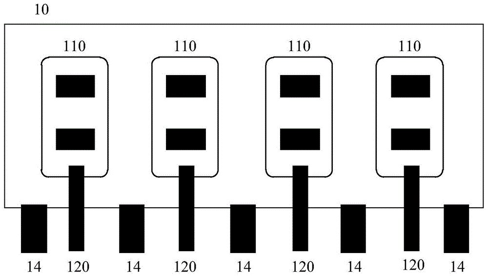
The embodiment provides a circuit board. Referring to fig. 1, fig. 1 shows a schematic layout of a circuit board 10 according to one embodiment. Wherein the circuit board 10 may be communicatively connected with another circuit board (not shown) for power delivery and information transfer. Illustratively, the circuit board 10 and the another circuit board may be various types of circuit boards, such as a ceramic circuit board, an alumina ceramic circuit board, an aluminum nitride ceramic circuit board, a Printed Circuit Board (PCB), an aluminum substrate, a high frequency board, a thick copper board, an ultra-thin circuit board, and the like, which the present invention is not limited thereto. Illustratively, the circuit board 10 may be any module board known in the art, such as a high power module board (e.g., an engine card, a graphics card, etc.) or the like, and the other circuit board may be a motherboard. Illustratively, the circuit board 10 may be a motherboard and the other circuit board may be any module board known in the art, such as a high power module board or the like. Further, the circuit board 10 may be a graphic card, and the other circuit board may be a motherboard, for example. It will be understood that this is merely exemplary and is not intended to limit the present invention.
Wherein the circuit board 10 may have at least one circuit component 110 bonded thereto, the circuit board 10 is shown in fig. 1 having four circuit components bonded thereto, but this is merely exemplary and not intended to be limiting. Illustratively, the circuit elements 110 may be bonded to the circuit board 10 by any method known in the art, for example, the circuit elements 110 may be soldered to the circuit board 10, may be bonded to the circuit board 10 by a tin-immersion method, or the like. The circuit element 110 may include any type of circuit element known in the art, such as an inductor, a capacitor, a resistor, a diode, a transistor, a MOS transistor, a MOSFET, etc., which is not limited in this respect. Wherein the circuit elements 110 may cooperate with (e.g., be integrated together) to perform a circuit function, e.g., form an analog integrated circuit such as an integrated operational amplifier, comparator, logarithmic and exponential amplifier, analog multiplier (divider), phase-locked loop, power management chip, etc., or form a digital integrated circuit such as a basic logic gate, flip-flop, register, decoder, driver, counter, shaping circuit, programmable logic device, microprocessor, single-chip, DSP, etc.
Here, the circuit component 110 may have at least one component connection portion 120, and the circuit component 110 is directly connected to another circuit board through the component connection portion 120. Thus, the current flowing through the circuit element 110 directly flows to another circuit board through the element connecting portion 120 without flowing through the circuit board 10 first and then flowing to another circuit board, reducing the direct current resistance and the alternating current resistance on the current path, thereby improving the power transmission performance. For example, the number of the element connecting portions 120 may be set as required, for example, 3, 4, 6, 8, and the like, which is not limited in the present invention.
In one embodiment, the component connection 120 may include at least one component pin 122. Referring to fig. 2, fig. 2 shows a schematic diagram of a circuit element according to an embodiment of the invention. Wherein circuit elements are shown including only element connections and other details of the circuit elements are omitted in order to not unnecessarily obscure the present invention.
As shown in fig. 2, the circuit element 110 includes two element pins 122, but this is merely exemplary and not intended to be limiting. The component pins 122 may be disposed on the edge side of the circuit component 110 close to the circuit board 10 and extend out of the outline of the circuit board 10, so that the circuit component 110 is directly connected to another circuit board through the component pins 122. Illustratively, the component leads 122 may be made of any suitable conductive material known in the art, such as copper, silver, etc., without limitation. For example, the number of the component pins 122 may be set according to the requirement, for example, 2, 3, 4, 6, etc., which is not limited in the present invention.
In one embodiment, component pins 122 may be bonded to another circuit board by any means known in the art.
In one embodiment, the other circuit board has a plurality of through holes, and the component pins 122 may be inserted into respective ones of the plurality of through holes to directly connect the circuit component 110 to the other circuit board. For good electrical connection between the circuit element 110 and another circuit board, the element pins 122 can be further soldered together after being inserted into the through holes of the other circuit board, and the pins can also be cut.
In another embodiment, another circuit board has a plurality of solder joints through which component pins 122 may be soldered (e.g., by Surface Mount Technology (SMT), Ball Grid Array (BGA) packaging technology, etc.) to the other circuit board to directly connect circuit component 110 to the other circuit board. It is to be understood that this is merely exemplary and not intended to be limiting and that the component pins 122 may also be joined to another circuit board by other methods known in the art.
To connect the circuit board 10 with another circuit board, in one embodiment, the circuit board 10 may include at least one board pin 14, and the board pin 14 may be disposed outside an edge of the circuit board 10 for connecting the circuit board 10 to another circuit board. Illustratively, the board pins 14 may be made of any suitable conductive material known in the art, such as copper, silver, etc., without limitation. The reason why the circuit board 10 is connected to another circuit board is that some components on the circuit board 10 may have no component connection parts, so that the components need to be power-transferred and information-transferred with another circuit board through the circuit board 10. The circuit board 10 is connected to another circuit board through board pins, which significantly reduces the connection impedance on the current path and improves the power transfer performance.
In one embodiment, board pins 14 may be plugged into respective ones of a plurality of through-holes of another circuit board to connect circuit board 10 to another circuit board. For good electrical connection between the circuit board 10 and another circuit board, the board pins 14 can be further soldered together after being inserted into the through holes of the other circuit board, and the pins can be cut.
In another embodiment, board pins 14 may be soldered to another circuit board through respective ones of the plurality of solder joints to connect circuit board 10 to another circuit board. It is to be understood that this is merely exemplary and not intended to be limiting, and that circuit board 10 may also be connected to another circuit board by other methods known in the art, such as by connectors, wires, etc.
In one embodiment, the component connection part 120 of the circuit component 110 may further include one or more through holes 124, and the circuit component 110 may be directly connected to another circuit board through the through holes 124. Referring to fig. 2, fig. 2 shows that the circuit element 110 includes two vias 124, but this is merely exemplary and not intended to be limiting.
In one embodiment, the other circuit board may include one or more pins that extend beyond the outline of the other circuit board and that may be inserted into the through holes 124 of the circuit element 110 to connect the circuit element 110 to the other circuit board. For good electrical connection between the circuit element 110 and another circuit board, the pin can be further soldered together after being inserted into the through hole 124 of the circuit element 110, and a pin trimming can also be performed.
In one embodiment, the circuit board 10 may further include one or more through holes (not shown), and a portion of the pins of another circuit board may be plugged into the through holes of the circuit board 10 to connect the circuit board 10 to the other circuit board. For good electrical connection between the circuit board 10 and another circuit board, after the pins are inserted into the through holes of the circuit board 10, the pins can be further soldered together, and pin trimming can also be performed.
Referring to fig. 3, fig. 3 shows a comparison of the current paths of a conventional circuit board and a circuit board of the present invention.
As can be seen from fig. 3, the circuit component on the circuit board of the present invention is directly connected to another circuit board through the component connection portion, so that the circuit component can directly transmit power to another circuit board, and has fewer connection points compared with the conventional circuit board, so that the present invention has a smaller direct current resistance on the direct current output path, and has a smaller alternating current resistance because the parasitic inductance is placed in front of the direct current output stage, thereby the present invention significantly improves the power transmission performance.
Example two
The present embodiment provides an arrangement and connection method of circuit boards. Wherein the circuit board can be communicatively coupled to another circuit board for power delivery and information transfer. Illustratively, the circuit board and the another circuit board may be various types of circuit boards, such as a ceramic circuit board, an alumina ceramic circuit board, an aluminum nitride ceramic circuit board, a Printed Circuit Board (PCB), an aluminum substrate, a high frequency board, a thick copper plate, an ultra-thin circuit board, and the like, which are not limited in this respect. Illustratively, the circuit board may be any module board known in the art, such as a high power module board (e.g., an engine card, a graphics card, etc.) or the like, and the other circuit board may be a motherboard. Illustratively, the circuit board may be a motherboard and the other circuit board may be any module board known in the art, such as a high power module board or the like. Further, the circuit board may be a graphic card, and the other circuit board may be a motherboard, for example. It will be understood that this is merely exemplary and is not intended to limit the present invention.
Referring to fig. 4, fig. 4 shows a flow chart of steps of a method 400 of arranging and connecting circuit boards according to one embodiment of the invention. As shown in fig. 4, the placement and connection method 400 may include the steps of:
at step 410, at least one component connection is provided on the circuit component.
At step 420, at least one circuit component is bonded to the circuit board, an
In step 430, the circuit component is directly connected to another circuit board through the component connection.
In one embodiment, the circuit elements may include any type of circuit element known in the art, such as inductors, capacitors, resistors, diodes, transistors, MOS transistors, MOSFETs, etc., and the present invention is not limited in this respect. Wherein the various circuit elements may cooperate with one another (e.g., be integrated together) to perform a circuit function, e.g., as an analog integrated circuit such as an integrated operational amplifier, comparator, logarithmic and exponential amplifier, analog multiplier (divider), phase-locked loop, power management chip, etc., or as a digital integrated circuit such as a basic logic gate, flip-flop, register, decoder, driver, counter, shaping circuit, programmable logic device, microprocessor, single-chip, DSP, etc.
In one embodiment, the circuit components may be bonded to the circuit board by any method known in the art, for example, the circuit components may be soldered to the circuit board, may be bonded to the circuit board by a solder-dipping method, and the like, but the invention is not limited thereto.
Illustratively, the circuit element may have at least one element connection portion. In one embodiment, the placement and connection method 400 may further include: the circuit component is directly connected to another circuit board through the component connection portion. Thus, the current flowing through the circuit element directly flows to another circuit board through the element connecting part without flowing through the circuit board first and then flowing to another circuit board, and the path area between the power supply voltage and the ground is reduced, thereby reducing the direct current resistance and the alternating current resistance and improving the power transmission performance. For example, the number of the element connecting portions may be set according to needs, for example, 3, 4, 6, 8, and the like, and the present invention is not limited thereto.
Illustratively, the component connection part may include at least one component pin. In one embodiment, the placement and connection method 400 may further include: the component pins are arranged on the side of the edge of the circuit component close to the circuit board and extend out of the outline of the circuit board so as to connect the circuit component directly to another circuit board through the component pins. For example, the component pins may be made of any suitable conductive material known in the art, such as copper, silver, etc., and the present invention is not limited thereto. For example, the number of component pins may be set according to the requirement, for example, 2, 3, 4, 6, and the like, which is not limited in the present invention.
For example, the component pins may be bonded to the circuit board by any means known in the art, and the invention is not limited thereto.
Illustratively, the other circuit board has a plurality of through holes (not shown). In one embodiment, the placement and connection method 400 may further include: component pins are inserted into respective ones of the plurality of through holes to directly connect the circuit component to another circuit board. For good electrical connection between the circuit element and another circuit board, after the element pin is inserted into the through hole of the other circuit board, the element pin and the through hole can be further welded together, and pin shearing can also be carried out.
Another circuit board illustratively has a plurality of solder bumps (not shown). In another embodiment, the placement and connection method 400 may further include: the component pins may be soldered (e.g., by Surface Mount Technology (SMT), Ball Grid Array (BGA) packaging technology, etc.) to another circuit board through respective ones of the plurality of solder joints to directly connect the circuit component to the other circuit board. It is to be understood that this is merely exemplary and not intended to be limiting and that the component pins may also be joined to another circuit board by other methods known in the art.
To connect a circuit board with another circuit board, in one embodiment, the placement and connection method 400 may further comprise: at least one board pin is provided on the circuit board, which board pin may be provided outside an edge of the circuit board for connecting the circuit board to another circuit board. For example, the board pins may be made of any suitable conductive material known in the art, such as copper, silver, etc., and the present invention is not limited thereto. The reason for connecting a circuit board to another circuit board is that some components on the circuit board may not have component connections, and thus these components need to be power-transferred and information-transferred through the circuit board to another circuit board.
In one embodiment, the placement and connection method 400 may further include: the board pins are inserted into respective ones of the plurality of through holes of another circuit board to connect the circuit board to the other circuit board. For good electrical connection between the circuit board and another circuit board, after the board pins are inserted into the through holes of the other circuit board, the two circuit boards can be further welded together, and pin shearing can also be performed.
In another embodiment, the placement and connection method 400 may further include: the board pins are soldered to another circuit board through respective ones of the plurality of solder joints to connect the circuit board to the other circuit board. It is to be understood that this is merely exemplary and not intended to be limiting and that the circuit board may be connected to another circuit board by other methods known in the art, such as by connectors, wires, etc.
Illustratively, the element connection part of the circuit element may further include one or more through holes. In one embodiment, the placement and connection method 400 may further include: the circuit elements are directly connected to another circuit board through the through holes.
Illustratively, the other circuit board may include one or more pins (not shown) that extend beyond the outline of the other circuit board. In one embodiment, the placement and connection method 400 may further include: the pin is inserted into a through hole of a circuit element to connect the circuit element to another circuit board. After the pin is inserted into the through hole of the circuit component, the pin and the circuit component can be further welded together, and pin shearing can be performed.
Illustratively, the circuit board may also include one or more vias (not shown). In one embodiment, the placement and connection method 400 may further include: some of the pins of another circuit board may be plugged into the through holes of the circuit board to connect the circuit board to the other circuit board. For good electrical connection between the circuit board and another circuit board, after the pins are inserted into the through holes of the circuit board, the pins can be further soldered together, and pin shearing can also be performed.
The circuit element on one circuit board is directly connected with another circuit board through the element connecting part, so that the circuit element can directly transmit power to the other circuit board, and has fewer connecting points compared with the conventional mode, therefore, the invention has smaller direct current resistance on a direct current output path, and has smaller alternating current resistance because parasitic inductance is arranged in front of a direct current output stage, thereby obviously improving the power transmission performance.
EXAMPLE III
The embodiment provides an electronic device. Illustratively, the electronic device may include any electronic device known in the art having more than one circuit board, such as a desktop computer, a laptop computer, a tablet computer, a smart home device, a cell phone, a robot, etc., without limitation. The electronic device of the present embodiment may include the circuit board according to the embodiment of the present invention described above.
Referring now to fig. 5, fig. 5 is a block diagram of one example electronic device 500 suitable for implementing at least some embodiments of the present disclosure. The electronic device 500 may include a bus 502 that directly or indirectly couples the following devices: memory 504, one or more Central Processing Units (CPUs) 506, one or more Graphics Processing Units (GPUs) 508, a communication interface 510, input/output (I/O) ports 512, input/output components 514, a power supply 516, and one or more presentation components 518 (e.g., one or more displays).
Although the various blocks of FIG. 5 are shown connected to the lines by a bus 502, this is not intended to be limiting, but only for the sake of clarity. For example, in some embodiments, a presentation component 518 (e.g., a display device) can be considered an I/O component 514 (e.g., if the display is a touch screen). As another example, CPU 506 and/or GPU 508 can include memory (e.g., memory 504 can represent a storage device in addition to memory of GPU 508, CPU 506, and/or other components). In other words, the electronic device of fig. 5 is merely illustrative. Categories such as "workstation," "server," "laptop," "desktop," "tablet," "client device," "mobile device," "handheld device," "gaming machine," "Electronic Control Unit (ECU)," "virtual reality system," "robotic device," and/or other device or system types are not distinguished as all categories are considered within the electronic device scope of fig. 5.
Bus 502 may represent one or more buses, such as an address bus, a data bus, a control bus, or a combination thereof. The bus 502 can include one or more bus types, such as an Industry Standard Architecture (ISA) bus, an Extended Industry Standard Architecture (EISA) bus, a Video Electronics Standard Association (VESA) bus, a Peripheral Component Interconnect (PCI) bus, a peripheral component interconnect express (PCIe) bus, and/or other types of buses.
Memory 504 may include any of a variety of computer-readable media. Computer readable media can be any available media that can be accessed by the electronic device 500. Computer readable media may include both volatile and nonvolatile media, and removable and non-removable media. By way of example, and not limitation, computer readable media may comprise computer storage media and communication media.
Computer storage media may include volatile and nonvolatile, and/or removable and non-removable media implemented in any method or technology for storage of information, such as computer readable instructions, data structures, program modules, and/or other data types. For example, memory 504 may store computer-readable instructions (e.g., instructions representing one or more programs and/or one or more program elements, such as an operating system). Computer storage media may include, but is not limited to, RAM, ROM, EEPROM, flash memory or other memory technology, CD-ROM, Digital Versatile Disks (DVD) or other optical disk storage, magnetic cassettes, magnetic tape, magnetic disk storage or other magnetic storage devices, or any other medium which can be used to store the desired information and which can accessed by electronic device 500. As used herein, computer storage media does not itself contain a signal.
Communication media may embody computer readable instructions, data structures, program modules, and/or other data types in a modulated data signal, such as a carrier wave or other transport mechanism, and includes any information delivery media. The term "modulated data signal" may refer to a signal that has one or more of its characteristics set or changed in such a manner as to encode information in the signal. By way of example, and not limitation, communication media may include wired media such as a wired network or direct-wired connection, and wireless media such as acoustic, RF, infrared and other wireless media. Combinations of any of the above should also be included within the scope of computer readable media.
The one or more CPUs 506 may be configured to execute computer-readable instructions to control one or more components of the electronic device 500 to perform one or more of the methods and/or processes described herein. Each of the one or more CPUs 506 can include one or more cores (e.g., one, two, four, eight, twenty-eight, seventy-two, etc.) capable of processing multiple software threads simultaneously. The one or more CPUs 506 can include any type of processor, and can include different types of processors, depending on the type of electronic device 500 implemented (e.g., a less-core processor for mobile devices and a more-core processor for servers). For example, depending on the type of electronic device 500, the processor may be an ARM processor implemented using Reduced Instruction Set Computing (RISC) or may be a x86 processor implemented using Complex Instruction Set Computing (CISC). In addition to one or more microprocessors or auxiliary coprocessors, such as mathematical coprocessors, the electronic device 500 may also include one or more CPUs 506.
The electronic device 500 may render graphics (e.g., 3D graphics) using one or more GPUs 508. One or more GPUs 508 may include hundreds or thousands of cores capable of processing hundreds or thousands of software threads simultaneously. The one or more GPUs 508 may generate pixel data for an output image in response to rendering commands (e.g., received from the one or more CPUs 506 via the host interface). One or more GPUs 508 may include graphics memory, such as display memory, for storing pixel data. Display memory may be included as part of storage 504. The one or more GPUs 508 may include two or more GPUs running in parallel (e.g., via a link). When combined together, each GPU 508 can generate pixel data for different portions of an output image or different output images (e.g., a first GPU for a first image and a second GPU for a second image). Each GPU may include its own memory or may share memory with other GPUs.
In examples where the electronic device 500 does not include one or more GPUs 508, one or more CPUs 506 may be used to render graphics.
The communication interface 510 may include one or more receivers, transmitters, and/or transceivers that enable the electronic device 500 to communicate with other electronic devices via an electronic communication network (including wired and/or wireless communication). Communication interface 510 may include components and functionality to enable communication over any number of different networks, such as a wireless network (e.g., Wi-Fi, Z-wave, bluetooth LE, ZigBee, etc.), a wired network (e.g., communication over ethernet), a low-power wide area network (e.g., LoRaWAN, SigFox, etc.), and/or the internet, among others.
The I/O ports 512 can enable the electronic device 500 to be logically coupled to other devices, including I/O components 514, one or more presentation components 518, and/or other components, some of which can be built into (e.g., integrated within) the electronic device 500. Illustrative I/O components 514 include a microphone, mouse, keyboard, joystick, game pad, game controller, satellite dish, scanner, printer, wireless device, and the like. The I/O component 514 may provide a Natural User Interface (NUI) that handles user-generated air gestures, voice, or other physiological inputs. In some cases, the input may be transmitted to an appropriate network element for further processing. The NUI may enable voice recognition, stylus recognition, facial recognition, biometric recognition, on-screen and near-screen gesture recognition, air gestures, head and eye tracking, and touch recognition (described in more detail below) associated with a display of the electronic device 500. The electronic device 500 may include a depth camera (e.g., a stereo camera system), an infrared camera system, an RGB camera system, touch screen technology, and combinations of these for gesture detection and recognition. Further, the electronic device 500 may include an accelerometer or gyroscope (e.g., as part of an Inertial Measurement Unit (IMU)) for detecting motion. In some examples, the output of the accelerometer or gyroscope may be used by electronic device 500 to present immersive augmented reality or virtual reality.
The power source 516 may include a hard-wired power source, a battery power source, or a combination thereof. The power supply 516 may provide power to the electronic device 500 to enable operation of the components of the electronic device 500.
One or more presentation components 518 may include a display (e.g., a monitor, touch screen, television screen, Heads Up Display (HUD), other display types, or combinations thereof), speakers, and/or other presentation components. One or more presentation components 518 may receive data from other components (e.g., one or more GPUs 508, one or more CPUs 506, etc.) and output data (e.g., images, video, sound, etc.).
Example operating Environment
In accordance with some embodiments of the present disclosure, the electronic device 500 may be implemented in the example operating environment 600 of fig. 6.
Operating environment 600 includes, among other components not illustrated, one or more client devices 620, one or more networks 640, one or more server devices 660, and one or more data stores 650. It is to be appreciated that the operating environment 600 illustrated in FIG. 6 is an example of one suitable operating environment. Each of the components shown in fig. 6 may be implemented via any type of computing device, such as, for example, one or more electronic devices 500 described in connection with fig. 5. These components may communicate with each other via a network 640, which may be wired, wireless, or both. Network 640 may include multiple networks or a network of networks, but is shown in simplified form so as not to obscure aspects of the present disclosure. By way of example, the network 640 may include one or more Wide Area Networks (WANs), one or more Local Area Networks (LANs), one or more public networks such as the internet, and/or one or more private networks. Where the network 640 comprises a wireless telecommunications network, components such as base stations, communication towers, or even access points (among other components) may provide wireless connectivity.
It should be understood that any number of client devices 620, server devices 660, and data stores 650 may be employed within operating environment 600 within the scope of the present disclosure. Each may be configured as a single device or as multiple devices cooperating in a distributed environment.
One or more client devices 620 may include at least some of the components, features, and functions of example electronic device 500 described herein with respect to fig. 5. By way of example and not limitation, client device 620 may embody a Personal Computer (PC), a laptop computer, a mobile device, a smartphone, a tablet computer, a smart watch, a wearable computer, a Personal Digital Assistant (PDA), an MP3 player, a Global Positioning System (GPS) or device, a video player, a handheld communication device, a gaming device or system, an entertainment system, an in-vehicle computer system, an embedded system controller, a remote control, an appliance, a consumer electronic device, a workstation, any combination of these depicted devices, or any other suitable device.
One or more client devices 620 may include one or more processors and one or more computer-readable media. The computer-readable medium may include computer-readable instructions executable by one or more processors. The instructions, when executed by one or more processors, may cause the one or more processors to perform the desired functions.
The one or more server devices 660 may also include one or more processors and one or more computer-readable media. The computer-readable medium includes computer-readable instructions executable by one or more processors. The instructions, when executed by one or more processors, may cause the one or more processors to perform the desired functions.
The one or more data stores 650 can include one or more computer-readable media. The computer-readable medium may include computer-readable instructions executable by one or more processors. The instructions, when executed by one or more processors, may cause the one or more processors to perform the desired functions. One or more data stores 650 (or computer data stores) are depicted as a single component, but may be embodied as one or more data stores (e.g., databases), and may be at least partially in the cloud.
Although depicted as being external to one or more server devices 660 and one or more client devices 620, one or more data stores 650 can be implemented, at least in part, on any combination of one or more server devices 660 and/or one or more client devices 620 (e.g., as memory 504 of fig. 5). For example, some information may be stored on one or more client devices 620, and other and/or duplicate information may be stored externally (e.g., on one or more server devices 660). Thus, it should be appreciated that information in one or more data stores 650 may be distributed across one or more data stores for storage (which may be hosted externally) in any suitable manner. For example, the one or more data stores 650 can include at least some of the one or more computer-readable media of the one or more server devices 660 and/or at least some of the one or more computer-readable media of the one or more client devices 620.
Although the illustrative embodiments have been described herein with reference to the accompanying drawings, it is to be understood that the foregoing illustrative embodiments are merely exemplary and are not intended to limit the scope of the invention thereto. Various changes and modifications may be effected therein by one of ordinary skill in the pertinent art without departing from the scope or spirit of the present invention. All such changes and modifications are intended to be included within the scope of the present invention as set forth in the appended claims.
In the description provided herein, numerous specific details are set forth. It is understood, however, that embodiments of the invention may be practiced without these specific details. In some instances, well-known methods, structures and techniques have not been shown in detail in order not to obscure an understanding of this description.
Similarly, it should be appreciated that in the description of exemplary embodiments of the invention, various features of the invention are sometimes grouped together in a single embodiment, figure, or description thereof for the purpose of streamlining the invention and aiding in the understanding of one or more of the various inventive aspects. However, the method of the present invention should not be construed to reflect the intent: that the invention as claimed requires more features than are expressly recited in each claim. Rather, as the following claims reflect, inventive aspects lie in less than all features of a single disclosed embodiment. Thus, the claims following the detailed description are hereby expressly incorporated into this detailed description, with each claim standing on its own as a separate embodiment of this invention.
It will be understood by those skilled in the art that all of the features disclosed in this specification (including any accompanying claims, abstract and drawings), and all of the processes or elements of any method or apparatus so disclosed, may be combined in any combination, except combinations where such features are mutually exclusive. Each feature disclosed in this specification (including any accompanying claims, abstract and drawings) may be replaced by alternative features serving the same, equivalent or similar purpose, unless expressly stated otherwise.
Furthermore, those skilled in the art will appreciate that while some embodiments described herein include some features included in other embodiments, rather than other features, combinations of features of different embodiments are meant to be within the scope of the invention and form different embodiments. For example, in the claims, any of the claimed embodiments may be used in any combination.
It should be noted that the above-mentioned embodiments illustrate rather than limit the invention, and that those skilled in the art will be able to design alternative embodiments without departing from the scope of the appended claims. In the claims, any reference signs placed between parentheses shall not be construed as limiting the claim. The word "comprising" does not exclude the presence of elements or steps not listed in a claim. The word "a" or "an" preceding an element does not exclude the presence of a plurality of such elements. The invention may be implemented by means of hardware comprising several distinct elements, and by means of a suitably programmed computer. In the unit claims enumerating several means, several of these means may be embodied by one and the same item of hardware. The usage of the words first, second and third, etcetera do not indicate any ordering. These words may be interpreted as names.
The above description is only for the specific embodiment of the present invention or the description thereof, and the protection scope of the present invention is not limited thereto, and any person skilled in the art can easily conceive of the changes or substitutions within the technical scope of the present invention, and the changes or substitutions should be covered within the protection scope of the present invention. The protection scope of the present invention shall be subject to the protection scope of the claims.