CN114041085B - Image pickup apparatus - Google Patents
Image pickup apparatus Download PDFInfo
- Publication number
- CN114041085B CN114041085B CN202080042622.4A CN202080042622A CN114041085B CN 114041085 B CN114041085 B CN 114041085B CN 202080042622 A CN202080042622 A CN 202080042622A CN 114041085 B CN114041085 B CN 114041085B
- Authority
- CN
- China
- Prior art keywords
- band
- light
- pixel
- polarization
- wavelength
- Prior art date
- Legal status (The legal status is an assumption and is not a legal conclusion. Google has not performed a legal analysis and makes no representation as to the accuracy of the status listed.)
- Active
Links
Images


Classifications
-
- G—PHYSICS
- G02—OPTICS
- G02B—OPTICAL ELEMENTS, SYSTEMS OR APPARATUS
- G02B5/00—Optical elements other than lenses
- G02B5/30—Polarising elements
- G02B5/3025—Polarisers, i.e. arrangements capable of producing a definite output polarisation state from an unpolarised input state
-
- H—ELECTRICITY
- H04—ELECTRIC COMMUNICATION TECHNIQUE
- H04N—PICTORIAL COMMUNICATION, e.g. TELEVISION
- H04N23/00—Cameras or camera modules comprising electronic image sensors; Control thereof
- H04N23/10—Cameras or camera modules comprising electronic image sensors; Control thereof for generating image signals from different wavelengths
- H04N23/11—Cameras or camera modules comprising electronic image sensors; Control thereof for generating image signals from different wavelengths for generating image signals from visible and infrared light wavelengths
-
- G—PHYSICS
- G02—OPTICS
- G02B—OPTICAL ELEMENTS, SYSTEMS OR APPARATUS
- G02B5/00—Optical elements other than lenses
- G02B5/20—Filters
- G02B5/201—Filters in the form of arrays
-
- G—PHYSICS
- G03—PHOTOGRAPHY; CINEMATOGRAPHY; ANALOGOUS TECHNIQUES USING WAVES OTHER THAN OPTICAL WAVES; ELECTROGRAPHY; HOLOGRAPHY
- G03B—APPARATUS OR ARRANGEMENTS FOR TAKING PHOTOGRAPHS OR FOR PROJECTING OR VIEWING THEM; APPARATUS OR ARRANGEMENTS EMPLOYING ANALOGOUS TECHNIQUES USING WAVES OTHER THAN OPTICAL WAVES; ACCESSORIES THEREFOR
- G03B11/00—Filters or other obturators specially adapted for photographic purposes
-
- H—ELECTRICITY
- H04—ELECTRIC COMMUNICATION TECHNIQUE
- H04N—PICTORIAL COMMUNICATION, e.g. TELEVISION
- H04N23/00—Cameras or camera modules comprising electronic image sensors; Control thereof
-
- H—ELECTRICITY
- H04—ELECTRIC COMMUNICATION TECHNIQUE
- H04N—PICTORIAL COMMUNICATION, e.g. TELEVISION
- H04N23/00—Cameras or camera modules comprising electronic image sensors; Control thereof
- H04N23/10—Cameras or camera modules comprising electronic image sensors; Control thereof for generating image signals from different wavelengths
- H04N23/125—Colour sequential image capture, e.g. using a colour wheel
-
- H—ELECTRICITY
- H04—ELECTRIC COMMUNICATION TECHNIQUE
- H04N—PICTORIAL COMMUNICATION, e.g. TELEVISION
- H04N25/00—Circuitry of solid-state image sensors [SSIS]; Control thereof
- H04N25/10—Circuitry of solid-state image sensors [SSIS]; Control thereof for transforming different wavelengths into image signals
- H04N25/11—Arrangement of colour filter arrays [CFA]; Filter mosaics
- H04N25/13—Arrangement of colour filter arrays [CFA]; Filter mosaics characterised by the spectral characteristics of the filter elements
- H04N25/135—Arrangement of colour filter arrays [CFA]; Filter mosaics characterised by the spectral characteristics of the filter elements based on four or more different wavelength filter elements
Abstract
The invention provides an imaging device for imaging a multispectral image with a frequency band of 4 or more. An imaging device (1) is provided with an imaging optical system (10), an image sensor (100), and a signal processing unit (200). The imaging optical system (10) has a band-pass filter unit (16) and a polarization filter unit (18) near the pupil, at least one of the aperture regions of the band-pass filter unit (16) transmits light of a plurality of wavelength bands, and the polarization filter unit (18) polarizes the light transmitted through the band-pass filter unit (16) in a plurality of directions. An image sensor (100) receives light after transmission through a plurality of spectral filtering elements and a plurality of polarization filtering elements. A signal processing unit (200) generates a plurality of image signals by processing a signal output from an image sensor (100). In an imaging device (1), the number of transmission bands of at least one opening region of a band-pass filter unit (16) is equal to or less than the number of transmission bands of a spectral filter element.
Description
Technical Field
The present invention relates to an imaging apparatus.
Background
Prior art documents
Patent literature
Patent document 1: international publication No. 2014/020791
Disclosure of Invention
One embodiment according to the present technology provides an imaging device that images a multispectral image of 4 bands or more.
Means for solving the technical problems
(1) An image pickup apparatus, comprising: an imaging optical system including a1 st optical element and a2 nd optical element in the vicinity of a pupil of the imaging optical system, the 1 st optical element having a plurality of opening regions, at least one of the opening regions transmitting light of a plurality of wavelength bands, the 2 nd optical element polarizing light transmitted through the 1 st optical element in a plurality of directions; an image sensor that receives light transmitted through the image pickup optical system, and receives light after transmitting a plurality of types of 3 rd optical elements different in transmission wavelength band and a plurality of types of 4 th optical elements different in transmission polarization direction; and a signal processing unit for generating a plurality of image signals by processing signals output from the image sensor, wherein the number of transmission bands of at least one of the opening regions of the 1 st optical element is equal to or less than the number of transmission bands of the 3 rd optical element.
(2) In the imaging device of the above (1), the 1 st optical element transmits light of a plurality of wavelength bands through all the aperture regions.
(3) In the imaging device according to the above (1), at least one of the opening regions of the 1 st optical element transmits light of one wavelength band.
(4) In the imaging device according to any one of (1) to (3) above, the 2 nd optical element allows a part of the light transmitted through the 1 st optical element to pass through as unpolarized light.
(5) In the imaging device according to the above (1) or (2), the number of the opening regions provided in the 1 st optical element is equal to or less than the number of the transmission polarization directions of the 4 th optical element, and all the opening regions have the same number of transmission bands as the number of transmission bands of the 3 rd optical element.
(6) In the imaging device according to any one of the above (1) to (4), at least one of the open regions of the 1 st optical element has a transmission wavelength band that partially overlaps with the plurality of wavelength bands of the 3 rd optical element.
(7) In the imaging device according to any one of (1) to (6), the imaging optical system and the image sensor satisfy a relationship of k ≦ m × n, where k is the number of transmission bands of the imaging optical system, m is the number of transmission bands of the 3 rd optical element, and n is the number of transmission polarization directions of the 4 th optical element.
(8) In the image pickup device of any one of the above (1) to (7), at least one set of the opening regions of the 1 st optical element transmits light of the same wavelength band.
(9) In the imaging device according to any one of (1) to (8), at least one opening region of the 1 st optical element is arranged on the optical axis.
(10) In the imaging device according to any one of (1) to (9) above, the signal processing unit generates a plurality of image signals by performing the interference cancellation processing.
Drawings
Fig. 1 is a diagram showing a schematic configuration of an imaging apparatus according to embodiment 1 of the present invention.
Fig. 2 is a front view of the band pass filter unit.
Fig. 3 is a graph showing the transmission wavelength characteristics of the 1 st band-pass filter.
Fig. 4 is a graph showing the transmission wavelength characteristics of the 2 nd band-pass filter.
Fig. 5 is a front view of the polarization filter unit.
Fig. 6 is a diagram showing a schematic configuration of an arrangement of pixels of an image sensor.
Fig. 7 is a diagram showing a schematic configuration of an image sensor.
Fig. 8 is a cross-sectional view showing a schematic configuration of one pixel (a dotted line portion of fig. 7).
Fig. 9 is a diagram showing an example of an arrangement pattern of the polarization filter elements provided in each pixel block.
Fig. 10 is a graph showing an example of the transmission wavelength characteristics of the 1 st spectral filter element.
Fig. 11 is a graph showing an example of the transmission wavelength characteristics of the 2 nd spectral filter element.
Fig. 12 is a diagram showing an example of an arrangement pattern of spectral filter elements provided in each pixel block.
Fig. 13 is a block diagram showing a schematic configuration of the signal processing unit.
Fig. 14 is a conceptual diagram of image generation.
Fig. 15 is a conceptual diagram of the operation of the imaging apparatus.
Fig. 16 is a front view of a polarization filter unit provided in the imaging device according to embodiment 2.
Fig. 17 is a front view of the band-pass filter unit.
Fig. 18 is a graph showing the transmission wavelength characteristics of the 1 st band-pass filter.
Fig. 19 is a graph showing the transmission wavelength characteristics of the 2 nd band-pass filter.
Fig. 20 is a graph showing the transmission wavelength characteristics of the 3 rd bandpass filter.
Fig. 21 is a front view of the polarization filter unit.
Fig. 22 is a graph showing the transmission wavelength characteristics of the 2 nd bandpass filter of the image pickup device according to embodiment 4.
Fig. 23 is an explanatory diagram of the transmission wavelength characteristics realized by the combination of the 2 nd band-pass filter and the 1 st spectral filter element.
Fig. 24 is an explanatory diagram of the transmission wavelength characteristics realized by the combination of the 2 nd band-pass filter and the 2 nd spectral filter element.
Fig. 25 is a diagram showing an example of an arrangement pattern of polarization filter elements provided in each pixel block of the imaging device according to embodiment 5.
Fig. 26 is a front view of a band-pass filter unit provided in the imaging optical system according to embodiment 6.
Fig. 27 is a graph showing the transmission wavelength characteristics of the 1 st band-pass filter.
Fig. 28 is a graph showing the transmission wavelength characteristics of the 2 nd band-pass filter.
Fig. 29 is a graph showing the transmission wavelength characteristics of the 3 rd bandpass filter.
Fig. 30 is a front view of a polarization filter unit provided in the imaging optical system according to embodiment 6.
Fig. 31 is a diagram showing a schematic configuration of an arrangement of pixels of an image sensor.
Fig. 32 is a diagram showing an example of an arrangement pattern of the polarization filter elements provided in each pixel block.
Fig. 33 is a graph showing an example of the transmission wavelength characteristics of the 1 st spectral filter element.
Fig. 34 is a graph showing an example of the transmission wavelength characteristics of the 2 nd spectral filter element.
Fig. 35 is a graph showing an example of the transmission wavelength characteristics of the 3 rd spectral filter element.
Fig. 36 is a diagram showing an example of an arrangement pattern of spectral filter elements provided in each pixel block.
Fig. 37 is a conceptual diagram of the operation of the imaging apparatus according to embodiment 6.
Fig. 38 is a diagram showing another example of the band pass filter unit.
Fig. 39 is a diagram showing another example of the polarization filter unit.
Fig. 40 is a diagram showing another example of the polarization filter unit.
Fig. 41 is a diagram showing another example of the band pass filter unit.
Fig. 42 is a diagram showing another example of the polarization filter unit.
Fig. 43 is a graph showing another example of the transmission wavelength characteristics set in the 1 st band-pass filter.
Fig. 44 is a graph showing another example of the transmission wavelength characteristics set in the 2 nd band-pass filter.
Fig. 45 is a graph showing another example of the transmission wavelength characteristics set in the 3 rd band-pass filter.
Fig. 46 is a front view of a band-pass filter unit provided in the imaging optical system according to embodiment 7.
Fig. 47 is a front view of a polarization filter unit provided in the imaging optical system according to embodiment 7.
Fig. 48 is a diagram showing a schematic configuration of an arrangement of pixels of an image sensor.
Fig. 49 is a diagram showing an example of an arrangement pattern of the polarization filter elements provided in each pixel block.
Fig. 50 is a diagram showing an example of an arrangement pattern of spectral filter elements provided in each pixel block.
Fig. 51 is a conceptual diagram of the operation of the imaging apparatus according to embodiment 7.
Fig. 52 is a front view showing an example of the band pass filter unit according to embodiment 8.
Fig. 53 is a front view showing another example of the band pass filter unit according to embodiment 8.
Fig. 54 is a front view showing an example of the band pass filter unit.
Fig. 55 is a front view showing an example of the polarization filter unit.
Detailed Description
Hereinafter, preferred embodiments of the present invention will be described in detail with reference to the accompanying drawings.
EXAMPLE 1 embodiment
[ Structure of imaging device ]
Fig. 1 is a diagram showing a schematic configuration of an imaging apparatus according to embodiment 1 of the present invention.
The imaging device of the present embodiment is an imaging device that captures a 4-band multispectral image. The imaging device of the present embodiment mainly includes an imaging optical system 10, an image sensor 100, and a signal processing unit 200.
[ image pickup optical System ]
The imaging optical system 10 is configured by combining a plurality of lenses 12. The imaging optical system 10 has a band-pass filter unit 16 and a polarization filter unit 18 in the vicinity of the pupil thereof. The imaging optical system 10 includes a focus adjustment mechanism, not shown. The focus adjustment mechanism adjusts the focus by moving the entire imaging optical system 10 back and forth along the optical axis L, for example.
Fig. 2 is a front view of the band pass filter unit.
The band pass filter unit 16 is an example of the 1 st optical element. The band pass filter unit 16 includes a housing 16A having two opening regions 16A1 and 16A2, and two band pass filters 16B1 and 16B2 provided in the housing 16A. In the following, one opening region 16A1 provided in the housing 16A is referred to as A1 st opening region 16A1, and the other opening region 16A2 is referred to as A2 nd opening region 16A2, as necessary, to distinguish the two opening regions 16Al, 16A2. The band pass filter 16B1 provided in the 1 st aperture region 16Al is referred to as a1 st band pass filter 16B1, and the band pass filter 16B2 provided in the 2 nd aperture region 16A2 is referred to as A2 nd band pass filter 16B2, thereby distinguishing the two band pass filters 16B1 and 16B2.
The two opening regions 16A1 and 16A2 provided in the housing 16A have a circular opening shape and are arranged symmetrically with respect to the optical axis L. The frame 16A has a light-shielding property, and allows only light to pass through the two opening regions 16A1 and 16A2.
The 1 st band-pass filter 16B1 and the 2 nd band-pass filter 16B2 are constituted by so-called multi-band-pass filters, and transmit light of a plurality of wavelength bands, respectively. In the imaging device of the present embodiment, the 1 st band-pass filter 16B1 and the 2 nd band-pass filter 16B2 transmit light of two wavelength bands, respectively. The 1 st band-pass filter 16B1 and the 2 nd band-pass filter 16B2 transmit light of different wavelength bands.
Fig. 3 is a graph showing the transmission wavelength characteristics of the 1 st band-pass filter.
As shown in fig. 3, the 1 st band-pass filter 16B1 transmits light in the wavelength band λ 11 and light in the wavelength band λ 12.
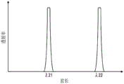
Fig. 4 is a graph showing the transmission wavelength characteristics of the 2 nd band-pass filter.
As shown in fig. 4, the 2 nd band-pass filter 16B2 transmits light in the wavelength band λ 21 and light in the wavelength band λ 22.
Fig. 5 is a front view of the polarization filter unit.
The polarization filter unit 18 is an example of the 2 nd optical element. The polarization filter unit 18 polarizes light transmitted through the band pass filter unit 16 in a plurality of directions. The polarization filter unit 18 includes a housing 18A having two opening regions 18A1 and 18A2, and one polarization filter 18B2 provided in one opening region 18A2 of the housing 18A. In the following, one opening region 18A1 provided in the housing 18A is referred to as A1 st opening region 18A1, and the other opening region 18A2 is referred to as A2 nd opening region 18A2, as necessary, to distinguish the two opening regions 18A1, 18A2. The polarization filter 18B2 is disposed in the 2 nd opening region 18A2.
The frame 18A has a light shielding property, and allows only light to pass through the two opening regions 18A1 and 18A2. The two opening regions 18A1 and 18A2 correspond to the two opening regions 16A1 and 16A2 of the band-pass filter unit 16, and are arranged in the same overlapping position. That is, the 1 st aperture region 18A1 has the same opening shape (circular shape) as the 1 st aperture region 16A1 of the band-pass filter unit 16, and is arranged to overlap at the same position. The 2 nd aperture region 18A2 has the same aperture shape as the 2 nd aperture region 16A2 of the band-pass filter unit 16, and is arranged to overlap at the same position. Accordingly, the light after passing through the 1 st opening region 16A1 of the band pass filter unit 16 passes through the 1 st opening region 18A1 of the polarization filter unit 18, and the light after passing through the 2 nd opening region 16A2 of the band pass filter unit 16 passes through the 2 nd opening region 18A2 of the polarization filter unit 18.
The polarization filter 18B2 provided in the 2 nd opening region 18A2 transmits light having a polarization direction θ (for example, azimuth angle 60 °). The polarization direction (polarization orientation) is represented by an angle (azimuth angle) that the polarization transmission axis makes with the x-axis (horizontal axis) on the xy-plane orthogonal to the optical axis L.
The polarization filter is disposed only in the 2 nd opening region 18A2. Therefore, the 1 st opening region 18A1 transmits unpolarized light.
In the imaging optical system 10 configured as described above, the pupil area is divided into two areas by the band-pass filter unit 16 and the polarization filter unit 18. That is, the pupil division is performed so as to divide the pupil division into A1 st pupil area defined by the 1 st opening region 16A1 of the band pass filter unit 16 and the 1 st opening region 18A1 of the polarization filter unit 18 and A2 nd pupil area defined by the 2 nd opening region 16A2 of the band pass filter unit 16 and the 2 nd opening region 18A2 of the polarization filter unit 18. Light of different characteristics is emitted from each pupil region. That is, unpolarized light of wavelength band λ 11 (1 st light), unpolarized light of wavelength band λ 12 (2 nd light), light of polarization direction θ of wavelength band λ 21 (3 rd light), and light of polarization direction θ of wavelength band λ 22 (4 th light) are emitted. The 1 st light and the 2 nd light are light after passing through the 1 st aperture region 16A1 of the band pass filter unit 16 and the 1 st aperture region 18A1 of the polarization filter unit 18. The 3 rd and 4 th lights are lights after passing through the 2 nd opening region 16A2 of the band pass filter unit 16 and the 2 nd opening region 18A2 of the polarization filter unit 18.
[ image sensor ]
Fig. 6 is a diagram showing a schematic configuration of an arrangement of pixels of an image sensor.
As shown in fig. 6, the image sensor 100 has a plurality of types of pixels P1, P2, P3, and P4 on its light receiving surface. The pixels P1 to P4 are regularly arranged at a predetermined pitch in the horizontal direction (x-axis direction) and the vertical direction (y-axis direction).
The image sensor 100 of the present embodiment is configured such that one pixel block PB (X, Y) is formed by 4 (2 × 2) pixels P1 to P4 adjacent to each other, and the pixel blocks PB (X, Y) are regularly arranged in the horizontal direction (X-axis direction) and the vertical direction (Y-axis direction). Hereinafter, the pixels P1 to P4 are divided as necessary, with the pixel P1 being the 1 st pixel P1, the pixel P2 being the 2 nd pixel P2, the pixel P3 being the 3 rd pixel P3, and the pixel P4 being the 4 th pixel P4. The pixels P1 to P4 have different optical characteristics.
Fig. 7 is a diagram showing a schematic configuration of an image sensor. Fig. 8 is a cross-sectional view showing a schematic configuration of one pixel (a dotted line portion of fig. 7).
The image sensor 100 has a pixel array layer 110, a polarization filter element array layer 120, a spectral filter element array layer 130, and a microlens array layer 140. Each layer is provided with a pixel array layer 110, a polarization filter element array layer 120, a spectral filter element array layer 130, and a microlens array layer 140 in this order from the image plane side toward the object side.
The pixel array layer 110 is configured by two-dimensionally arranging a plurality of photodiodes 112. One photodiode 112 constitutes one pixel. The photodiodes 112 are regularly arranged in the horizontal direction (x-axis direction) and the vertical direction (y-axis direction).
The polarization filter array layer 120 is configured by two-dimensionally arranging two types of polarization filter elements 122A and 122B having different transmission polarization directions (polarization directions of transmitted light). Hereinafter, the polarization filter elements 122A and 122B are distinguished from each other by taking the polarization filter element 122A as the 1 st polarization filter element 122A and the polarization filter element 122B as the 2 nd polarization filter element 122B, as necessary. The polarization filter elements 122A and 122B are arranged at the same interval as the photodiode 112, and are provided for each pixel. The 1 st polarization filter element 122A transmits light of the 1 st polarization direction θ 1 (for example, azimuth angle 90 °). The 2 nd polarization filter element 122B transmits light of a2 nd polarization direction θ 2 (for example, azimuth angle 0 °) different from the 1 st polarization direction θ 1. The polarization filter elements 122A and 122B are examples of the 4 th optical element.
In each pixel block PB (X, Y), polarization filter elements 122A, 122B are regularly arranged.
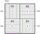
Fig. 9 is a diagram showing an example of an arrangement pattern of the polarization filter elements provided in each pixel block.
As shown in fig. 9, in the imaging device according to the present embodiment, the 1 st pixel P1 and the 4 th pixel P4 in the pixel block are provided with the 1 st polarization filter 122A, and the 2 nd pixel P2 and the 3 rd pixel P3 are provided with the 2 nd polarization filter 122B.
The spectral filter array layer 130 is configured by two-dimensionally arranging two types of spectral filter elements 132A and 132B having different transmission wavelength characteristics from each other. Hereinafter, the spectral filter elements 132A and 132B are divided into the 1 st spectral filter element 132A and the 2 nd spectral filter element 132B by the spectral filter element 132A and the spectral filter element 132B, respectively, as necessary. The spectral filter elements 132A and 132B are arranged at the same interval as the photodiode 112, and are provided for each pixel. The spectral filter elements 132A and 132B are examples of the 3 rd optical element.
Fig. 10 is a graph showing an example of the transmission wavelength characteristics of the 1 st spectral filter element. Fig. 11 is a graph showing an example of the transmission wavelength characteristics of the 2 nd spectral filter element.
As shown in fig. 10, the 1 st spectral filter element 132A transmits light of the wavelength band λ a. On the other hand, as shown in fig. 11, the 2 nd spectral filter element 132B transmits light of a wavelength band λ B different from that of the 1 st spectral filter element 132A.
As shown in fig. 10 and 11, in the band-pass filter unit 16 provided in the imaging optical system 10, the wavelength bands λ 11 and λ 12 that the 1 st band-pass filter 16B1 allows transmission and the wavelength bands λ 21 and λ 22 that the 2 nd band-pass filter 16B2 allows transmission are set within the range of the transmission wavelength band λ a of the 1 st spectral filter element 132A and the transmission wavelength band λ B of the 2 nd spectral filter element 132B. Specifically, the wavelength band λ 11 that the 1 st band-pass filter 16B1 allows transmission and the wavelength band λ 21 that the 2 nd band-pass filter 16B2 allows transmission are set within the range of the transmission wavelength band λ a of the 1 st spectral filter element 132A. The wavelength band λ 12 that the 1 st band-pass filter 16B1 allows transmission and the wavelength band λ 22 that the 2 nd band-pass filter 16B2 allows transmission are set within the transmission wavelength band λ B of the 2 nd spectral filter element 132B.
Fig. 12 is a diagram showing an example of an arrangement pattern of spectral filter elements provided in each pixel block.
As shown in fig. 12, spectral filter elements 132A and 132B are regularly arranged in each pixel block PB (X, Y). In the imaging device of the present embodiment, the 1 st pixel P1 and the 2 nd pixel P2 are provided with the 1 st spectral filter element 132A, and the 3 rd pixel P3 and the 4 th pixel P4 are provided with the 2 nd spectral filter element 132B.
The microlens array layer 140 is configured by two-dimensionally arranging a plurality of microlenses 142. The microlenses 142 are arranged at the same intervals as the photodiodes 112, and are provided for each pixel. The microlens 142 is provided for the purpose of efficiently condensing light from the imaging optical system 10 on the photodiode 112.
In the image sensor 100 configured as described above, the pixels P1 to P4 in each pixel block PB (X, Y) receive light from the imaging optical system 10 as follows. That is, the 1 st pixel P1 receives light from the imaging optical system 10 via the 1 st spectral filter element 132A (wavelength λ a) and the 1 st polarization filter element 122A (polarization direction θ 1). The 2 nd pixel P2 receives light from the imaging optical system 10 via the 1 st spectral filter element 132A (wavelength λ a) and the 2 nd polarization filter element 122B (polarization direction θ 2). The 3 rd pixel P3 receives light from the imaging optical system 10 via the 2 nd spectral filter element 132B (wavelength band λ B) and the 2 nd polarization filter element 122B (polarization direction θ 2). The 4 th pixel P4 receives light from the imaging optical system 10 via the 2 nd spectral filter element 132B (wavelength band λ B) and the 1 st polarization filter element 122A (polarization direction θ 1). In this way, the pixels P1 to P4 of the pixel block PB (X, Y) receive light of different wavelength bands and different polarization characteristics by the spectral filter elements 132A and 132B and the polarization filter elements 122A and 122B having different combinations, respectively.
[ Signal processing section ]
The signal processing unit 200 generates an image signal (image data) of a 4-band multispectral image by processing a signal output from the image sensor 100. That is, image signals of four kinds of wavelength bands λ 11, λ 12, λ 21, λ 22 of the band pass filter unit 16 of the transmission imaging optical system 10 are generated.
Fig. 13 is a block diagram showing a schematic configuration of the signal processing unit.
As shown in fig. 13, the signal processing unit 200 includes an analog signal processing unit 200A, an image generating unit 20OB, and a coefficient storage unit 200C.
The analog signal processing unit 200A reads an analog pixel signal output from each pixel of the image sensor 100, performs predetermined signal processing (for example, correlated double sampling processing, amplification processing, and the like), converts the analog pixel signal into a digital signal, and outputs the digital signal.
The image generating unit 200B performs predetermined signal processing on the pixel signals converted into digital signals to generate image signals of the respective wavelength bands λ 11, λ 12, λ 21, and λ 22.
Fig. 14 is a conceptual diagram of image generation.
Each pixel block PB (X, Y) includes a1 st pixel P1, a2 nd pixel P2, a3 rd pixel P3, and a4 th pixel P4. Therefore, the four image signals D1 to D4 can be generated by separating and extracting the pixel signals of the 1 st pixel P1, the 2 nd pixel P2, the 3 rd pixel P3, and the 4 th pixel P4 from the pixel blocks PB (X, Y). However, interference (crosstalk) occurs in the four image signals. That is, since light of each wavelength band is incident on each of the pixels P1 to P4, the generated image is an image in which images of each wavelength band are mixed at a predetermined ratio. Therefore, the image generating unit 200B generates image signals of each wavelength band by performing the interference removal processing.
The interference cancellation process performed by the signal processing unit 200 will be described below.
A pixel signal (signal value) obtained from the 1 st pixel P1 of each pixel block PB (X, Y) is α 1, a pixel signal obtained from the 2 nd pixel P2 is α 2, a pixel signal obtained from the 3 rd pixel P3 is α 3, and a pixel signal obtained from the 4 th pixel P4 is α 4. Four pixel signals α 1 to α 4 are obtained from each pixel block PB (X, Y). The image generating unit 200B calculates four pixel signals β 1 to β 4 corresponding to the light of the respective wavelength bands λ 11, λ 12, λ 21, and λ 22 from the four pixel signals α 1 to α 4, and removes the interference. Specifically, four pixel signals β 1 to β 4 corresponding to light of the respective bands λ 11, λ 12, λ 21, λ 22 are calculated by using expression 1 of the following matrix a, and the interference is removed.
[ numerical formula 1]

[ numerical formula 2]

The pixel signal β 1 is a pixel signal corresponding to light in the wavelength band λ 11, the pixel signal β 2 is a pixel signal corresponding to light in the wavelength band λ 12, the pixel signal β 3 is a pixel signal corresponding to light in the wavelength band λ 21, and the pixel signal β 4 is a pixel signal corresponding to light in the wavelength band λ 22. Therefore, an image signal of the wavelength band λ 11 is generated from the pixel signal β 1, an image signal of the wavelength band λ 12 is generated from the pixel signal β 2, an image signal of the wavelength band λ 21 is generated from the pixel signal β 3, and an image signal of the wavelength band λ 22 is generated from the pixel signal β 4. The reason why the interference can be removed by the above equation 1 will be described below.
The interference occurs due to the light of each wavelength band λ 11, λ 12, λ 21, λ 22 mixing into each of the pixels P1 to P4. The ratio (interference ratio) of the light in each wavelength band λ 11, λ 12, λ 21, λ 22 emitted from the imaging optical system 10 to be received by each of the pixels P1 to P4 is bij (i =1 to 4, j =1 to 4). Here, b11 is a proportion of the light of the wavelength band λ 11 received by the 1 st pixel P1, b12 is a proportion of the light of the wavelength band λ 12 received by the 1 st pixel P1, b13 is a proportion of the light of the wavelength band λ 21 received by the 1 st pixel P1, and b14 is a proportion of the light of the wavelength band λ 22 received by the 1 st pixel P1. And, b21 is a proportion of the light of the wavelength band λ 11 received by the 2 nd pixel P2, b22 is a proportion of the light of the wavelength band λ 12 received by the 2 nd pixel P2, b23 is a proportion of the light of the wavelength band λ 21 received by the 2 nd pixel P2, and b24 is a proportion of the light of the wavelength band λ 22 received by the 2 nd pixel P2. And, b31 is a proportion of the light of the wavelength band λ 11 received by the 3 rd pixel P3, b32 is a proportion of the light of the wavelength band λ 12 received by the 3 rd pixel P3, b33 is a proportion of the light of the wavelength band λ 21 received by the 3 rd pixel P3, and b34 is a proportion of the light of the wavelength band λ 22 received by the 3 rd pixel P3. And, b41 is a proportion of the light of the wavelength band λ 11 received by the 4 th pixel P4, b42 is a proportion of the light of the wavelength band λ 12 received by the 4 th pixel P4, b43 is a proportion of the light of the wavelength band λ 21 received by the 4 th pixel P4, and b44 is a proportion of the light of the wavelength band λ 22 received by the 4 th pixel P4. The ratio bij is uniquely determined by a transmission band and a transmission polarization direction (including non-polarization) set in the imaging optical system 10 and a transmission band and a transmission polarization direction set in each pixel of the image sensor 100. That is, the polarization direction is uniquely determined by a combination of the transmission wavelength band set in each of the opening regions 16A1 and 16A2 of the band pass filter unit 16 and the transmission wavelength band set in each of the spectral filter elements 132A and 132B of the image sensor 100, and a combination of the transmission polarization direction (including non-polarization) set in each of the opening regions 18A1 and 18A2 of the polarization filter unit 18 and the polarization direction set in each of the polarization filter elements 122A and 122B of the image sensor 100. Therefore, the ratio bij at which the light in each wavelength band λ 11, λ 12, λ 21, λ 22 emitted from the imaging optical system 10 is received by each of the pixels P1 to P4 can be obtained in advance.
The following relationship is established between the pixel signals α 1 to α 4 obtained from the pixels P1 to P4 of the pixel blocks PB (X, Y) and the pixel signals β 1 to β 4 corresponding to the light of the respective wavelength bands λ 11, λ 12, λ 21, λ 22.
Regarding the pixel signal α 1 obtained from the 1 st pixel P1, "b11 × β 1+ b12 × β 2+ b13 × β 3+ b14 × β 4= α 1 \8230;" 8230 "; expression 2" holds (") is a symbol of an integrating calculation).
Regarding the pixel signal α 2 obtained from the 2 nd pixel P2, "b21 × β 1+ b22 × β 2+ b23 × β 3+ b24 × β 4= α 2 \8230; formula 3" holds.
Regarding the pixel signal α 3 obtained from the 3 rd pixel P3, "b31 × β 1+ b32 × β 2+ b33 × β 3+ b34 × β 4= α 3 \8230 \ 8230 '; equation 4' holds.
Regarding the pixel signal α 4 obtained from the 4 th pixel P4, "b41 × β 1+ b42 × β 2+ b43 × β 3+ b44 × 4= α 4 \8230'; 8230; equation 5" holds.
Here, the simultaneous equations of the above equations 2 to 5 can be expressed by the following equation 6 using the matrix B.
[ numerical formula 3]

[ numerical formula 4]

Solutions of the simultaneous equations of the above equations 2 to 5, i.e., β 1 to β 4, can be obtained by multiplying the inverse matrix B of the matrix B on both sides of the above equation 6 -1 To calculate.
[ numerical formula 5]

In this way, the pixel signals β 1 to β 4 corresponding to the respective wavelength bands λ 11, λ 12, λ 21, and λ 22 can be calculated from the signal values (pixel signals) α 1 to α 4 of the respective pixels P1 to P4 based on the ratio at which the light of the respective wavelength bands λ 11, λ 12, λ 21, and λ 22 emitted from the imaging optical system 10 is received by the respective pixels P1 to P4 of the pixel block PB (X, Y).
In the above formula 1, the inverse matrix B of the above formula 7 is -1 Is set as A (B) -1 = a). Therefore, each element aij of the matrix a in equation 1 can be obtained by obtaining the inverse matrix B of the matrix B -1 To obtain.
The coefficient storage unit 200C stores each element aij of the matrix a for performing the interference cancellation process as a coefficient group.
The image generating unit 200B acquires the coefficient group from the coefficient storage unit 200C, calculates pixel signals β 1 to β 4 corresponding to the respective bands λ 11, λ 12, λ 21, λ 22 from the pixel signals α 1 to α 4 obtained from the respective pixels P1 to P4 of the respective pixel blocks PB (X, Y) by the above expression 1, and generates image signals of the respective bands λ 11, λ 12, λ 21, λ 22.
The image signals of the respective bands λ 11, λ 12, λ 21, λ 22 generated by the image generator 200B are output to the outside, and are stored in a storage device (not shown) as needed. And displayed on a display (not shown) as necessary.
[ Effect of the image pickup apparatus ]
Fig. 15 is a conceptual diagram of the operation of the imaging apparatus according to the present embodiment.
The light incident on the imaging optical system 10 becomes four types of light having different characteristics, and is incident on the image sensor 100. Specifically, unpolarized light having a wavelength band λ 11 (1 st light), unpolarized light having a wavelength band λ 12 (2 nd light), light having a polarization direction θ having a wavelength band λ 21 (3 rd light), and light having a polarization direction θ having a wavelength band λ 22 (4 th light) enter the image sensor 100.
In each pixel block PB (X, Y) of the image sensor 100, light in each wavelength band emitted from the imaging optical system 10 is received by each of the pixels P1 to P4 at a predetermined ratio. That is, the light of each wavelength band is received at a predetermined ratio bij by the action of the polarization filter elements 122A, 122B and the spectral filter elements 132A, 132B provided in the pixels Pl to P4.
The signal processing unit 200 calculates pixel signals β 1 to β 4 corresponding to light of the respective wavelength bands λ 11, λ 12, λ 21, λ 22 from pixel signals α 1 to α 4 obtained from the respective pixels P1 to P4 of the respective pixel blocks PR (X, Y) of the image sensor 100, and generates image signals of the respective wavelength bands λ 11, λ 12, λ 21, λ 22. That is, an arithmetic process (interference elimination process) based on equation 1 using the matrix a is performed, pixel signals β 1 to β 4 corresponding to light of the respective wavelength bands λ 11, λ 12, λ 21, λ 22 are calculated from pixel signals α 1 to α 4 of the respective pixels P1 to P4 obtained from the image sensor 100, and image signals of the respective wavelength bands λ 11, λ 12, λ 21, λ 22 are generated.
As described above, according to the image pickup apparatus of the present embodiment, it is possible to capture images of four wavelength bands (multi-spectral images of 4 frequency bands) by one image pickup optical system 10 and one (single-plate) image sensor 100.
In the imaging device of the present embodiment, the band-pass filter unit 16 of the imaging optical system 10 transmits light of a plurality of wavelength bands through one opening region. This makes it possible to increase the aperture size as compared with a structure in which light in each wavelength band is extracted separately. This can improve the sensitivity. In particular, by setting the number of transmission bands set in each opening region (the number of transmission bands of the band pass filter provided in each opening region) to the same number as the number of transmission bands of the image sensor (the number of types of spectral filter elements provided in the image sensor), the opening size can be increased as much as possible, and the sensitivity can be improved.
In the imaging device of the present embodiment, one aperture region is set to pass through the polarization filter unit 18 of the imaging optical system 10. This can prevent a decrease in the amount of light due to polarization. Therefore, this configuration also improves the sensitivity. With this configuration, it is also possible to simultaneously capture polarization images.
EXAMPLE 2
The imaging device of the present embodiment is different from the imaging device of embodiment 1 in that polarization filters 18B1 and 18B2 are provided in two opening regions, i.e., A1 st opening region 18A1 and A2 nd opening region 16A2 of a polarization filter unit 18. The other configuration is the same as that of the imaging device according to embodiment 1. Therefore, only the structure of the polarization filter unit 18 will be explained here.
Fig. 16 is a front view of a polarization filter unit provided in the imaging device of the present embodiment.
As shown in fig. 16, polarization filters 18B1 and 18B2 are provided in the 1 st aperture region 18A1 and the 2 nd aperture region 18A2. Hereinafter, the two polarization filters 18B1 and 18B2 are distinguished by using the polarization filter 18B1 disposed in the 1 st opening region 18A1 as the 1 st polarization filter 18B1 and using the polarization filter 18B1 disposed in the 2 nd opening region 18A2 as the 2 nd polarization filter 18B2. The 1 st polarization filter 18B1 transmits light of the 1 st polarization direction θ 1 (for example, azimuth angle 150 °). The 2 nd polarization filter 18B2 transmits light of a2 nd polarization direction θ 2 (for example, azimuth angle 60 °) different from the 1 st polarization direction θ 1. In this way, the polarization filter unit 18 can be provided with the polarization filters 18B1 and 18B2 in all the respective opening regions 18Al and 18A2 of the housing 18A.
In addition, when the polarization filter is provided in all the respective opening regions as in the present embodiment, one of the plurality of types of polarization filter elements provided in the image sensor may be configured to pass directly therethrough.
When a 4-band multispectral image is captured, the following configuration is adopted, thereby preventing interference. That is, the transmission polarization directions of the 1 st polarization filter 18B1 and the 2 nd polarization filter 18B2 provided in the polarization filter unit 18 are orthogonal to each other, and the transmission polarization directions of the 1 st polarization filter element 122A and the 2 nd polarization filter element 122B provided in the image sensor 100 are orthogonal to each other. For example, a polarization filter that transmits light having an azimuth angle of 90 ° is used for the 1 st polarization filter 18B1 of the polarization filter unit 18, and a polarization filter that transmits light having an azimuth angle of 0 ° is used for the 2 nd polarization filter 18B2. On the other hand, a1 st polarization filter element 122A of the image sensor 100 is a polarization filter element that transmits light having an azimuth angle of 90 °, and a2 nd polarization filter element 122B is a polarization filter element that transmits light having an azimuth angle of 0 °. Thus, the image sensor 100 can receive light of each separated wavelength band. Therefore, the signal processing unit 200 can generate the image signals of each wavelength band without performing the interference cancellation process.
EXAMPLE 3 rd embodiment
The imaging device of the present embodiment is different from the imaging device of embodiment 1 in the configurations of the band-pass filter unit 16 and the polarization filter unit 18. The other configuration is the same as that of the imaging device according to embodiment 1. Therefore, only the configurations of the polarization filter unit 18 and the band pass filter unit 16 will be described here.
Fig. 17 is a front view of the band-pass filter unit.
As shown in fig. 17, the band-pass filter unit 16 of the present embodiment has three opening regions 16A1, 16A2, and 16A3. Hereinafter, the opening region 16A1 is referred to as A1 st opening region 16A1, the opening region 16A2 is referred to as A2 nd opening region 16A2, and the opening region 16A3 is referred to as A3 rd opening region 16A3 as necessary, to thereby distinguish the three opening regions 16A1, 16A2, and 16A3.
The 1 st opening region 16Al has a rectangular opening shape and is disposed in a region that equally divides one side of the frame 16A. The 2 nd opening region 16A2 and the 3 rd opening region 16A3 each have a circular opening shape and are disposed in a region that equally divides the other side of the frame 16A.
Band pass filters 16B1, 16B2, and 16B3 having different transmission wavelength bands are provided in the respective opening regions 16A1 to 16A3. Hereinafter, the bandpass filter 16B1 provided in the 1 st opening region 16A1 is referred to as A1 st bandpass filter 16B1, the bandpass filter 16B2 provided in the 2 nd opening region 16A2 is referred to as A2 nd bandpass filter 16B2, and the bandpass filter 16B3 provided in the 3 rd opening region 16A3 is referred to as A3 rd bandpass filter 16B3, thereby distinguishing the three bandpass filters 16B1, 16B2, and 16B3.
Fig. 18 is a graph showing the transmission wavelength characteristics of the 1 st band-pass filter.
As shown in fig. 18, the 1 st band-pass filter 16B1 is constituted by a so-called multi-band-pass filter which transmits light of two wavelength bands. Specifically, light in the wavelength band λ 11 and light in the wavelength band λ 12 are transmitted. The graphs of the two wavelength bands λ a, λ B shown by the broken lines in fig. 18 are graphs of the transmission wavelength characteristics of the 1 st spectral filter element 132A and the 2 nd spectral filter element 132B provided in the image sensor 100, respectively (the graph of the wavelength band λ a is a graph of the transmission wavelength characteristics of the 1 st spectral filter element 132A, and the graph of the wavelength band λ B is a graph of the transmission wavelength characteristics of the 2 nd spectral filter element 132B). The wavelength bands λ 11, λ 12 that the 1 st band-pass filter 16B1 allows transmission are set within the ranges of the wavelength bands λ a, λ B that the 1 st spectral filter element 132A and the 2 nd spectral filter element 132B allow transmission. Specifically, one wavelength band λ 11 is set in the range of the wavelength band λ a that the 1 st spectral filter element 132A allows transmission, and the other wavelength band λ 12 is set in the range of the wavelength band λ B that the 2 nd spectral filter element 132B allows transmission.
Fig. 19 is a graph showing the transmission wavelength characteristics of the 2 nd band-pass filter.
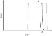
As shown in fig. 19, the 2 nd band-pass filter 16B2 transmits light of one wavelength band. Specifically, light in the wavelength band λ 2 is transmitted. In addition, the graph of the wavelength band λ a shown by the broken line in fig. 19 is a graph of the transmission wavelength characteristic of the 1 st spectral filter element 132A provided in the image sensor 100. The wavelength band λ 2 that the 2 nd band-pass filter 16B2 allows transmission is set within the range of the wavelength band λ a that the 1 st spectral filtering element 132A allows transmission.
Fig. 20 is a graph showing the transmission wavelength characteristics of the 3 rd band-pass filter.
As shown in fig. 20, the 3 rd band-pass filter 16B3 transmits light of one wavelength band. Specifically, as shown in fig. 20, light in the wavelength band λ 3 is transmitted. In addition, the graph of the wavelength band λ B shown by the broken line in fig. 20 is a graph of the transmission wavelength characteristic of the 2 nd spectral filter element 132B provided in the image sensor 100. The wavelength band λ 3 that the 3 rd band-pass filter 16B3 allows transmission is set within the range of the wavelength band λ B that the 2 nd spectral filter element 132B allows transmission.
Fig. 21 is a front view of the polarization filter unit.
As shown in fig. 21, the polarization filter unit 18 has three opening regions 18A1, 18A2, and 18A3 in the frame 18A, similarly to the band-pass filter unit 16. Hereinafter, the opening region 18A1 is referred to as A1 st opening region 18A1, the opening region 18A2 is referred to as A2 nd opening region 18A2, and the opening region 18A3 is referred to as A3 rd opening region 18A3, whereby the three opening regions 18A1, 18A2, and 18A3 are distinguished.
Each of the opening regions 18A1 to 18A3 has the same opening shape as the corresponding opening region 16A1 to 16A3 in the band-pass filter unit 16, and is arranged in the same position in an overlapping manner. Therefore, the light having passed through each of the aperture regions 16A1 to 16A3 of the band-pass filter unit 16 enters the corresponding aperture region 18A1 to 18A3.
The 1 st opening region 18A1 is provided to pass directly. Accordingly, unpolarized light passes through the 1 st opening region 18A1.
The 2 nd aperture region 18A2 and the 3 rd aperture region 18A3 are provided with a polarization filter 18B2. The polarization filter 18B2 transmits light of a polarization direction θ (for example, azimuth angle 60 °).
According to the image pickup device having the above configuration, the light having passed through the 1 st opening region 16A1 of the band pass filter unit 16 passes through the 1 st opening region 18A1 of the polarization filter unit 18, and is incident on the image sensor 100. After passing through the 2 nd opening region 16A2 of the band pass filter unit 16, the light passes through the 2 nd opening region 18A2 of the polarization filter unit 18 and is incident on the image sensor 100. After passing through the 3 rd opening region 16A3 of the band pass filter unit 16, the light passes through the 3 rd opening region 18A3 of the polarization filter unit 18 and is incident on the image sensor 100.
The 1 st opening region 16A1 of the band pass filter unit 16 is provided with a band pass filter (1 st band pass filter 16B 1) that transmits light of two wavelength bands λ 11, λ 12. In the 2 nd aperture region 16A2 and the 3 rd aperture region 16A3, band pass filters (A2 nd band pass filter 16B2 and A3 rd band pass filter 16B 3) for transmitting light of one wavelength band λ 2 and λ 3 are provided. Therefore, four kinds of light having different characteristics are emitted from the imaging optical system 10. That is, unpolarized light of wavelength band λ 11 (1 st light), unpolarized light of wavelength band λ 12 (2 nd light), light of polarization direction θ of wavelength band λ 21 (3 rd light), and light of polarization direction θ of wavelength band λ 22 (4 th light) are emitted. Therefore, the imaging device of the present embodiment can also capture images of four wavelength bands (4-band multispectral images) in the same manner as the imaging device of embodiment 1.
In the present embodiment, the 1 st aperture region 18A1 of the polarization filter unit 18 is set to pass directly, but a polarization filter for polarizing the passed light in a predetermined polarization direction may be provided as in the above-described 2 nd embodiment.
EXAMPLE 4 th embodiment
The imaging apparatus of the present embodiment is different from the imaging apparatus of embodiment 1 in the configuration of the band-pass filter unit 16. Specifically, the 2 nd bandpass filter 16B2 provided in the 2 nd aperture region 16A2 of the bandpass filter unit 16 has a transmission wavelength characteristic different from that of the imaging device according to embodiment 1. The other configuration is the same as that of the imaging device according to embodiment 1. Therefore, only the transmission wavelength characteristics of the 2 nd band-pass filter 16B2 will be described here.
Fig. 22 is a graph showing the transmission wavelength characteristics of the 2 nd bandpass filter of the image pickup apparatus according to the present embodiment.
In fig. 22, the graph of the wavelength band λ a indicated by a broken line is a graph of the transmission wavelength characteristic of the 1 st spectral filter element 132A provided in the image sensor 100, and the graph of the wavelength band λ B indicated by a broken line is a graph of the transmission wavelength characteristic of the 2 nd spectral filter element 132B.
As shown in fig. 22, the 2 nd bandpass filter 16B2 provided in the image pickup apparatus of the present embodiment transmits light of one wavelength band λ 2. The transmission band is set to span the transmission band of the 1 st spectral filter element 132A and the transmission band of the 2 nd spectral filter element 132B provided to the image sensor 100. In other words, a part of the transmission band is set to overlap with the transmission band of the 1 st spectral filter element 132A and the transmission band of the 2 nd spectral filter element 132B.
By using the 2 nd band-pass filter 16B2 of the above structure, the image sensor 100 substantially receives light of four wavelength bands. That is, the light transmitted through the 2 nd bandpass filter 16B2 is light of one wavelength band λ 2, but is substantially separated into two wavelength bands by the 1 st spectral filter element 132A and the 2 nd spectral filter element 132B. Therefore, the light of four kinds of wavelength bands is received together with the light of two wavelength bands separated by the 1 st band-pass filter 16B1.
Fig. 23 is an explanatory diagram of the transmission wavelength characteristics realized by the combination of the 2 nd band-pass filter and the 1 st spectral filter element. As shown in fig. 23, when light having passed through the 2 nd band-pass filter 16B2 enters, the pixel provided with the 1 st spectral filter element 132A receives light in a wavelength band indicated by diagonal lines. That is, light of a wavelength band λ 2A in which the 2 nd band-pass filter 16B2 allows transmission and a wavelength band λ 2A in which the 1 st spectral filtering element 132A allows transmission overlap with the wavelength band λ a is received.
Fig. 24 is an explanatory diagram of the transmission wavelength characteristics realized by the combination of the 2 nd band-pass filter and the 2 nd spectral filter element. As shown in fig. 24, when light having passed through the 2 nd band-pass filter 16B2 enters, the pixel provided with the 2 nd spectral filter element 132B receives light in a wavelength band indicated by oblique lines. That is, light of a wavelength band λ 2B in which the 2 nd band-pass filter 16B2 allows transmission and a wavelength band λ 2B in which the 2 nd spectral filter element 132B allows transmission overlap with the wavelength band λ B is received.
In this way, even if the 2 nd band-pass filter 16B2 is configured to transmit light of one wavelength band λ 2, light of two wavelength bands can be substantially separated by the 1 st spectral filter element 132A and the 2 nd spectral filter element 132B provided in the image sensor 100. In addition, with this configuration, the band pass filter can be simplified. Further, it is possible to reduce the wavelength shift that occurs when light enters obliquely with respect to the filter.
EXAMPLE 5 EXAMPLE
In the imaging device according to embodiment 1, when a multispectral image of 4 bands is captured, one pixel block is formed by four pixels, and the optical characteristics of each pixel are changed by combining two types of polarization filter elements and two types of spectral filter elements. Polarization filter elements having different polarization characteristics may be used for the polarization filter elements of the respective pixels provided in one pixel block. The following will be explained: when a multispectral image of 4 bands is captured, one pixel block is formed by four pixels, and polarization filter elements having different transmission polarization directions are provided in each pixel. The imaging apparatus is the same as the imaging apparatus according to embodiment 1 except that the arrangement of the polarization filter elements is different. Therefore, only the arrangement of the polarization filter elements will be described here.
Fig. 25 is a diagram showing an example of an arrangement pattern of polarization filter elements provided in each pixel block of the imaging device according to the present embodiment.
As shown in fig. 25, in the imaging device of the present embodiment, polarization filter elements 122A to 122D having different transmission polarization directions are provided in four pixels P1 to P4 constituting one pixel block PB (X, Y). Specifically, the 1 st pixel P1 is provided with the 1 st polarization filter element 122A that transmits light of the 1 st polarization direction θ 1 (e.g., 90 °). The 2 nd pixel P2 is provided with a2 nd polarization filter element 122B that transmits light of the 2 nd polarization direction θ 2 (for example, 0 °). The 3 rd pixel P3 is provided with a3 rd polarization filter element 122C that transmits light of the 3 rd polarization direction θ 3 (e.g., 45 °). The 4 th pixel P4 is provided with a4 th polarization filter element 122D that transmits light of the 4 th polarization direction θ 4 (e.g., 135 °).
The number of the opening regions provided in the band-pass filter unit may be set to be equal to or less than the number of transmission polarization directions of the image sensor (equal to or less than the number of types of polarization filter elements provided in the image sensor). In this case, the number of the transmission bands set in each of the opening regions is set to be the same as the number of the transmission bands of the image sensor, whereby the opening size can be increased as much as possible. In addition, the sensitivity can be improved thereby.
EXAMPLE 6 EXAMPLE
The imaging device of the present embodiment captures a 9-band multispectral image. The imaging apparatus is the same as the imaging apparatus according to embodiment 1 described above in that it includes the imaging optical system 10, the image sensor 100, and the signal processing unit 200 (see fig. 1).
[ image pickup optical System ]
The imaging optical system 10 of the imaging apparatus according to the present embodiment is different from the imaging optical system according to embodiment 1 in the configurations of the band-pass filter unit 16 and the polarization filter unit 18.
Fig. 26 is a front view of a band-pass filter unit provided in the imaging optical system of the present embodiment.
The band-pass filter unit 16 has three opening regions 16A1, 16A2, and 16A3 in the housing 16A. Hereinafter, the opening region 16Al is referred to as A1 st opening region 16A1, the opening region 16A2 is referred to as A2 nd opening region 16A2, and the opening region 16A3 is referred to as A3 rd opening region 16A3 as necessary, and the opening regions 16A1 to 16A3 are distinguished from each other.
The respective opening regions 16A1 to 16A3 have the same opening shape (rectangular shape), and are arranged symmetrically about the optical axis L. Specifically, the 2 nd opening region 16A2 is arranged on the optical axis, and the 1 st opening region 16A1 and the 3 rd opening region 16A3 are arranged symmetrically with the 2 nd opening region 16A2 interposed therebetween.
Band pass filters 16B1 to 16B3 having different transmission wavelength characteristics are provided in the respective aperture regions 16A1 to 16A3. Hereinafter, the bandpass filter 16B1 provided in the 1 st aperture region 16A1 is referred to as A1 st bandpass filter 16B1, the bandpass filter 16B2 provided in the 2 nd aperture region 16A2 is referred to as A2 nd bandpass filter 16B2, and the bandpass filter 16B3 provided in the 3 rd aperture region 16A3 is referred to as A3 rd bandpass filter 16B3, as necessary, to distinguish the bandpass filters 16B1 to 16B3.
Fig. 27 is a graph showing the transmission wavelength characteristics of the 1 st band-pass filter.
As shown in fig. 27, the 1 st band-pass filter 16B1 is composed of a multi-band-pass filter that transmits light of three wavelength bands. Specifically, light in the wavelength band λ 11, light in the wavelength bands λ 12 and λ 13 are transmitted.
Fig. 28 is a graph showing the transmission wavelength characteristics of the 2 nd band-pass filter.
As shown in fig. 28, the 2 nd band-pass filter 16B2 is also constituted by a multi-band-pass filter which transmits light of three wavelength bands. Specifically, light in the wavelength band λ 21, and light in the wavelength bands λ 22 and λ 23 are transmitted.
Fig. 29 is a graph showing the transmission wavelength characteristics of the 3 rd bandpass filter.
As shown in fig. 29, the 3 rd bandpass filter 16B3 is also composed of a multi-bandpass filter that transmits light of three wavelength bands. Specifically, light in the wavelength band λ 31, and light in the wavelength bands λ 32 and λ 33 are transmitted.
Fig. 30 is a front view of a polarization filter unit provided in the imaging optical system of the present embodiment.
As shown in fig. 30, the polarization filter unit 18 has three opening regions 18A1, 18A2, and 18A3 in the frame 18A. Hereinafter, the opening region 18A1 is referred to as A1 st opening region 18Al, the opening region 18A2 is referred to as A2 nd opening region 18A2, and the opening region 18A3 is referred to as A3 rd opening region 18A3, as necessary, to distinguish the opening regions 18A1 to 18A3 from each other.
The three opening regions 18A1, 18A2, and 18A3 correspond to the three opening regions 16A1, 16A2, and 16A3 of the band-pass filter unit 16, and are arranged in the same overlapping position. That is, the 1 st aperture region 18A1 has the same aperture shape as the 1 st aperture region 16A1 of the band-pass filter unit 16, and is arranged to overlap at the same position. The 2 nd aperture region 18A2 has the same aperture shape as the 2 nd aperture region 16A2 of the band-pass filter unit 16, and is arranged in the same position in an overlapping manner. The 3 rd aperture region 18A3 has the same aperture shape as the 3 rd aperture region 16A3 of the band-pass filter unit 16, and is arranged to overlap at the same position. Accordingly, light after passing through the 1 st opening region 16A1 of the band pass filter unit 16 passes through the 1 st opening region 18A1, light after passing through the 2 nd opening region 16A2 of the band pass filter unit 16 passes through the 2 nd opening region 18A2, and light after passing through the 3 rd opening region 16A3 of the band pass filter unit 16 passes through the 3 rd opening region 18A3.
The 2 nd aperture region 18A2 and the 3 rd aperture region 18A3 are provided with polarization filters 18B2 and 18B3 having different transmission polarization directions, respectively. Specifically, the 2 nd opening region 18A2 is provided with a polarization filter 18B2 that passes light having a polarization direction θ 2 (for example, an azimuth angle of 150 °). The 3 rd opening region 18A3 is provided with a polarization filter 18B3 that passes light having a polarization direction θ 3 (for example, an azimuth angle of 150 °).
The polarization filter is provided only in the 2 nd opening region 18A2 and the 3 rd opening region 18A3. Therefore, the 1 st opening region 18A1 transmits unpolarized light.
The imaging optical system 10 divides the pupil area into three areas by a combination of the band-pass filter unit 16 and the polarization filter unit 18. That is, the pupil division is performed into A1 st pupil region defined by the 1 st opening region 16A1 of the band pass filter unit 16 and the 1 st opening region 18A1 of the polarization filter unit 18, A2 nd pupil region defined by the 2 nd opening region 16A2 of the band pass filter unit 16 and the 2 nd opening region 18A2 of the polarization filter unit 18, and A3 rd pupil region defined by the 3 rd opening region 16A3 of the band pass filter unit 16 and the 3 rd opening region 18A3 of the polarization filter unit 18. Light of different characteristics is emitted from each pupil region. That is, unpolarized light of a wavelength band λ 11 (1 st light), unpolarized light of a wavelength band λ 12 (2 nd light), unpolarized light of a wavelength band λ 13 (3 rd light), light of a polarization direction θ 2 of a wavelength band λ 21 (4 th light), light of a polarization direction θ 2 of a wavelength band λ 22 (5 th light), light of a polarization direction θ 2 of a wavelength band λ 23 (6 th light), light of a polarization direction θ 3 of a wavelength band λ 31 (7 th light), light of a polarization direction θ 3 of a wavelength band λ 32 (8 th light), and light of a polarization direction θ 3 of a wavelength band λ 33 (9 th light) are emitted.
[ image sensor ]
Fig. 31 is a diagram showing a schematic configuration of an arrangement of pixels of an image sensor.
As shown in fig. 31, the image sensor 100 of the imaging apparatus according to the present embodiment includes a pixel block PB (X, Y) including 9 (3 × 3) pixels P1 to P9 adjacent to each other. Hereinafter, the pixels P1 to P9 are distinguished, as necessary, by using the pixel P1 as the 1 st pixel P1, the pixel P2 as the 2 nd pixel P2, the pixel P3 as the 3 rd pixel P3, the pixel P4 as the 4 th pixel P4, the pixel P5 as the 5 th pixel P5, the pixel P6 as the 6 th pixel P6, the pixel P7 as the 7 th pixel P7, the pixel P8 as the 8 th pixel P8, and the pixel P9 as the 9 th pixel P9.
The image sensor 100 is similar to the image pickup device according to embodiment 1 described above, in that it includes a pixel array layer 110, a polarization filter element array layer 120, a spectral filter element array layer 130, and a microlens array layer 140 (see fig. 7). The image sensor 100 of the present embodiment is different in the structure of the polarization filter array layer 120 and the spectral filter array layer 130.
Three types of polarization filter elements 122A, 122B, and 122C having different transmission polarization directions are provided in the polarization filter element array layer 120. Hereinafter, the polarization filter elements 122A to 122C are divided as necessary, with the polarization filter element 122A being the 1 st polarization filter element 122A, the polarization filter element 122B being the 2 nd polarization filter element 122B, and the polarization filter element 122C being the 3 rd polarization filter element 122C. The 1 st polarization filter element 122A transmits light having a polarization direction θ 1 (for example, azimuth angle 90 °). The 2 nd polarization filter element 122B transmits light having a polarization direction θ 2 (for example, azimuth angle 45 °). The 3 rd polarization filter element 122C transmits light having a polarization direction θ 3 (for example, azimuth angle 0 °).
Fig. 32 is a diagram showing an example of an arrangement pattern of the polarization filter elements provided in each pixel block.
As shown in fig. 32, the 1 st pixel P1, the 4 th pixel P4, and the 7 th pixel P7 are provided with a1 st polarization filter element 122A. The 2 nd pixel P2, the 5 th pixel P5, and the 8 th pixel P8 are provided with a2 nd polarization filter element 122B. The 3 rd, 6 th, and 9 th pixels P3, P6, and P9 are provided with a3 rd polarization filter element 122C.
The spectral filter array layer 130 is provided with three types of spectral filter elements 132A, 132B, and 132C having different transmission wavelength characteristics. Hereinafter, the spectral filter elements 132A to 132C are divided as necessary by using the spectral filter element 132A as the 1 st spectral filter element 132A, the spectral filter element 132B as the 2 nd spectral filter element 132B, and the spectral filter element 132C as the 3 rd spectral filter element 132C.
Fig. 33 is a graph showing an example of the transmission wavelength characteristics of the 1 st spectral filter element.
As shown in fig. 33, the 1 st spectral filter element 132A transmits light of a wavelength band λ a (e.g., red (Red, R) wavelength band). In the band pass filter unit 16 provided in the imaging optical system 10, the 1 st band pass filter 16B1 allows the transmission wavelength band λ 11, the 2 nd band pass filter 16B2 allows the transmission wavelength band λ 21, and the 3 rd band pass filter 16B3 allows the transmission wavelength band λ 31 to be set within the range of the transmission wavelength band λ a of the 1 st spectral filter element 132A.
Fig. 34 is a graph showing an example of the transmission wavelength characteristics of the 2 nd spectral filter element.
As shown in fig. 34, the 2 nd spectral filter element 132B transmits light of a wavelength band λ B (e.g., green (G) wavelength band). In the band pass filter unit 16 provided in the imaging optical system 10, a wavelength band λ 12 in which the 1 st band pass filter 16B1 allows transmission, a wavelength band λ 22 in which the 2 nd band pass filter 16B2 allows transmission, and a wavelength band λ 32 in which the 3 rd band pass filter 16B3 allows transmission are set within a range of the transmission wavelength band λ B of the 2 nd spectral filter element 132B.
Fig. 35 is a graph showing an example of the transmission wavelength characteristics of the 3 rd spectral filter element.
As shown in fig. 35, the 3 rd spectral filter element 132C transmits light of a wavelength band λ C (e.g., blue (B) wavelength band). In the band pass filter unit 16 provided in the imaging optical system 10, the 1 st band pass filter 16B1 allows transmission of a wavelength band λ 13, the 2 nd band pass filter 16B2 allows transmission of a wavelength band λ 23, and the 3 rd band pass filter 16B3 allows transmission of a wavelength band λ 33 within the range of the transmission wavelength band λ C of the 3 rd spectral filter element 132C.
Fig. 36 is a diagram showing an example of an arrangement pattern of spectral filter elements provided in each pixel block.
As shown in fig. 36, the 1 st pixel P1, the 2 nd pixel P2, and the 3 rd pixel P3 are provided with a1 st spectral filter element 132A. The 4 th, 5 th, and 6 th pixels P4, P5, and P6 are provided with the 2 nd spectral filter element 132B. The 7 th pixel P7, the 8 th pixel P8, and the 9 th pixel P9 are provided with a3 rd spectral filter element 132C.
In the image sensor 100 configured as described above, the pixels P1 to P9 in each pixel block PB (X, Y) receive light from the imaging optical system 10 as follows. That is, the 1 st pixel P1 receives light from the imaging optical system 10 via the 1 st spectral filter element 132A and the 1 st polarization filter element 122A. The 2 nd pixel P2 receives light from the imaging optical system 10 via the 1 st spectral filter 132A and the 2 nd polarization filter 122B. The 3 rd pixel P3 receives light from the imaging optical system 10 via the 1 st spectral filter 132A and the 3 rd polarization filter 122C. The 4 th pixel P4 receives light from the imaging optical system 10 via the 2 nd spectral filter 132B and the 1 st polarization filter 122A. The 5 th pixel P5 receives light from the imaging optical system 10 via the 2 nd spectral filter element 132B and the 2 nd polarization filter element 122B. The 6 th pixel P6 receives light from the imaging optical system 10 via the 2 nd spectral filter 132B and the 3 rd polarization filter 122C. The 7 th pixel P7 receives light from the imaging optical system 10 via the 3 rd spectral filter element 132C and the 1 st polarization filter element 122A. The 8 th pixel P8 receives light from the imaging optical system 10 via the 3 rd spectral filter element 132C and the 2 nd polarization filter element 122B. The 9 th pixel P9 receives light from the imaging optical system 10 via the 3 rd spectral filter element 132C and the 3 rd polarization filter element 122C. In this way, the pixels P1 to P9 of the pixel block PB (X, Y) receive light of different characteristics by the spectral filter elements 132A to 132C and the polarization filter elements 122A to 122C having different combinations, respectively.
[ Signal processing section ]
The signal processing unit 200 generates an image signal of a 9-band multispectral image by processing a signal output from the image sensor 100. That is, image signals of nine wavelength bands λ 11, λ 12, λ 13, λ 21, λ 22, λ 23, λ 31, λ 32, λ 33 of the band-pass filter unit 16 of the transmission imaging optical system 10 are generated. The signal processing unit 200 is similar to the signal processing unit 200 of embodiment 1 described above in that it performs a predetermined interference cancellation process to generate image signals of each wavelength band.
[ Effect of the image pickup apparatus ]
Fig. 37 is a conceptual diagram of the operation of the imaging apparatus according to the present embodiment.
The light incident on the imaging optical system 10 becomes nine types of light having different characteristics, and is incident on the image sensor 100. Specifically, unpolarized light (1 st light) of the wavelength band λ 11, unpolarized light (2 nd light) of the wavelength band λ 12, unpolarized light (3 rd light) of the wavelength band λ 13, light (4 th light) of the polarization direction θ 2 of the wavelength band λ 21, light (5 th light) of the polarization direction θ 2 of the wavelength band λ 22, light (6 th light) of the polarization direction θ 2 of the wavelength band λ 23, light (7 th light) of the polarization direction θ 3 of the wavelength band λ 31, light (8 th light) of the polarization direction θ 3 of the wavelength band λ 32, and light (9 th light) of the polarization direction θ 3 of the wavelength band λ 33 are incident on the image sensor 100.
In each pixel block PB (X, Y) of the image sensor 100, light emitted from the imaging optical system 10 is received by each of the pixels P1 to P9 at a predetermined ratio. That is, light in the wavelength band λ 11, light in the wavelength band λ 12, light in the wavelength band λ 13, light in the wavelength band λ 21, light in the wavelength band λ 22, light in the wavelength band λ 23, light in the wavelength band λ 31, light in the wavelength band λ 32, and light in the wavelength band λ 33 are received at a predetermined ratio.
The signal processing unit 200 calculates pixel signals β 1 to β 9 corresponding to light of the respective bands λ 11, λ 12, λ 13, λ 21, λ 22, λ 23, λ 31, λ 32, and λ 33 from the pixel signals α 1 to α 9 obtained from the respective pixels P1 to P9 of the respective pixel blocks PB (X, Y) of the image sensor 100, and generates image signals of the respective bands λ 11, λ 12, λ 13, λ 21, λ 22, λ 23, λ 31, λ 32, and λ 33.
As described above, according to the image pickup apparatus of the present embodiment, it is possible to capture a multispectral image of 9 frequency bands by one image pickup optical system 10 and one image sensor 100.
[ modifications of band-pass filter Unit and polarization Filter Unit ]
Fig. 38 is a diagram showing another example of the band pass filter unit. Fig. 39 is a diagram showing another example of the polarization filter unit.
As shown in fig. 38, in the band-pass filter unit 16 of the present example, the housing 16A has nine opening regions, and band-pass filters that transmit light of the respective wavelength bands λ 11, λ 12, λ 13, λ 21, λ 22, λ 23, λ 31, λ 32, and λ 33 are provided individually in the respective opening regions. Therefore, the light of each wavelength band λ 11, λ 12, λ 13, λ 21, λ 22, λ 23, λ 31, λ 32, λ 33 is separated by passing through each opening region.
As shown in fig. 39, in the polarization filter unit 18, the frame 18A also has nine opening regions corresponding to the band pass filter unit, and polarization filters are provided in the respective opening regions. In this example, three types of polarization filters (polarization directions θ 1, θ 2, and θ 3) having different transmission polarization directions are used in combination, but one of them may be unpolarized (directly passed).
Fig. 40 is a diagram showing another example of the polarization filter unit.
With respect to the polarization filter unit shown in fig. 39, in the polarization filter unit 18 of the present example, open regions having the same polarization characteristics are combined into one. In this way, by combining the open regions having the same polarization characteristic into one, the filter can be easily manufactured. In this case, the aperture shape (the shape seen through as the aperture region (the shape indicated by the broken line)) when overlapping the band pass filter unit 16 is the shape of the substantial aperture region (pupil region).
Fig. 41 is a diagram showing another example of the band pass filter unit. Fig. 42 is a diagram showing another example of the polarization filter unit.
As shown in fig. 41, in the bandpass filter unit 16 of the present example, the frame 16A has seven opening regions. One of the seven opening regions is provided with a multi-bandpass filter which transmits light of three wavelength bands λ 11, λ 12, λ 13. The remaining open regions are provided with bandpass filters which transmit light of one wavelength band λ 21, λ 22, λ 23, λ 31, λ 32, λ 33, respectively.
As shown in fig. 42, in the polarization filter unit 18, the frame 18A also has seven opening regions corresponding to the band pass filter unit. Polarization filters (polarization directions θ 1, θ 2, and θ 3) are provided in the respective opening regions.
As in this example, by appropriately using the multi-band-pass filter, the opening size can be increased. This can improve sensitivity.
Fig. 43 to 45 are graphs showing another example (modification) of the transmission wavelength characteristics of the respective bandpass filters set in the bandpass filter unit. Fig. 43 is a graph showing another example of the transmission wavelength characteristics set in the 1 st band-pass filter. Fig. 44 is a graph showing another example of the transmission wavelength characteristics set in the 2 nd band-pass filter. Fig. 45 is a graph showing another example of the transmission wavelength characteristic set in the 3 rd bandpass filter.
As shown in fig. 43, the 1 st band-pass filter transmits light of two wavelength bands λ 11, λ 12. Here, one wavelength band λ 11 is set to pass through the transmission wavelength bands λ a and λ B of the 1 st spectral filter element 132A and the 2 nd spectral filter element 132B provided in the image sensor 100. In other words, a part of the wavelength band is set to overlap with the transmission wavelength band λ a of the 1 st spectral filter element 132A and the transmission wavelength band λ B of the 2 nd spectral filter element 132B. The other wavelength band λ 12 is set within a range of a transmission wavelength band λ C of the 3 rd spectral filter element 132C provided to the image sensor 100.
As shown in fig. 44, the 2 nd band pass filter transmits light of three wavelength bands λ 21, λ 22, λ 23. Here, the wavelength band λ 21 is set within the range of the transmission wavelength band λ a of the 1 st spectral filter element 132A provided in the image sensor 100. Also, the wavelength band λ 22 is set within the range of the transmission wavelength band λ B of the 2 nd spectral filter element 132B provided in the image sensor 100. The wavelength band λ 23 is set within the transmission wavelength band λ C of the 3 rd spectral filter element 132C provided in the image sensor 100.
As shown in fig. 45, the 3 rd band pass filter transmits light of three wavelength bands λ 31, λ 32, λ 33. Here, the wavelength band λ 31 is set within the range of the transmission wavelength band λ a of the 1 st spectral filter element 132A provided in the image sensor 100. The wavelength band λ 32 is set within the range of the transmission wavelength band λ B of the 2 nd spectral filter element 132B provided in the image sensor 100. The wavelength band λ 33 is set within the range of the transmission wavelength band λ C of the 3 rd spectral filter element 132C provided in the image sensor 100.
According to the bandpass filter unit having the above configuration, in the imaging optical system, the lights of eight kinds of wavelength bands λ 11, λ 12, λ 21, λ 22, λ 23, λ 31, λ 32, λ 33 are separated. However, in the image sensor, light of nine wavelength bands can be received substantially. That is, the light of the wavelength band λ 11 separated by the 1 st band-pass filter is substantially separated into two wavelength bands by the 1 st spectral filter element 132A and the 2 nd spectral filter element 132B. Therefore, in the image sensor, light of nine wavelength bands can be received substantially.
(7 th embodiment)
The imaging device of the present embodiment captures a 12-band multispectral image. The imaging apparatus is the same as the imaging apparatus according to embodiment 1 described above in that it includes the imaging optical system 10, the image sensor 100, and the signal processing unit 200 (see fig. 1).
[ image pickup optical System ]
The imaging optical system of the imaging apparatus of the present embodiment is different from the imaging optical system 10 of the imaging apparatus 1 of embodiment 1 in the configurations of the band-pass filter unit 16 and the polarization filter unit 18.
Fig. 46 is a front view of a band-pass filter unit provided in the imaging optical system of the present embodiment.
The band-pass filter unit 16 has three opening regions (A1 st opening region 16A1, A2 nd opening region 16A2, and A3 rd opening region 16A 3) in the housing 16A. Band filters (A1 st band filter 16B1, a2 nd band filter 16B2, and A3 rd band filter 16B 3) having different transmission wavelength characteristics are provided in the respective opening regions 16A1 to 16A3. Each of the bandpass filters 16B1 to 16B3 is composed of a multi-bandpass filter that transmits light of four different wavelength bands. Specifically, the 1 st band-pass filter 16B1 transmits light in wavelength bands R λ 1, G λ 1, B λ 1, and IR λ 1. The 2 nd band-pass filter 16B2 transmits light in the wavelength bands R λ 2, G λ 2, B λ 2, IR λ 2. The 3 rd band pass filter 16B3 transmits light in the wavelength bands R λ 3, G λ 3, B λ 3, IR λ 3.
Fig. 47 is a front view of a polarization filter unit provided in the imaging optical system of the present embodiment.
As shown in fig. 47, the polarization filter unit 18 has three opening regions (A1 st opening region 18A1, A2 nd opening region 18A2, and A3 rd opening region 18A 3) in the frame 18A. Polarization filters (the 1 st polarization filter 18B1, the 2 nd polarization filter 18B2, and the 3 rd polarization filter 18B 3) having different transmission polarization directions are provided in the respective opening regions 18A1 to 18A3. Specifically, the 1 st polarization filter 18B1 transmits light in the polarization direction θ 1. The 2 nd polarization filter 18B2 transmits light of the polarization direction θ 2. The 3 rd polarization filter 18B3 transmits light of the polarization direction θ 3.
Twelve lights having different characteristics are emitted from the imaging optical system having the above configuration. That is, light of the polarization direction θ 1 of the wavelength band R λ 1 (1 st light), light of the polarization direction θ 1 of the wavelength band G λ 1 (2 nd light), light of the polarization direction θ 1 of the wavelength band B λ 1 (3 rd light), light of the polarization direction θ 1 of the wavelength band IR λ 1 (4 th light), light of the polarization direction θ 2 of the wavelength band R λ 2 (5 th light), light of the polarization direction θ 2 of the wavelength band G λ 2 (6 th light), light of the polarization direction θ 2 of the wavelength band B λ 2 (7 th light), light of the polarization direction θ 2 of the wavelength band IR λ 2 (8 th light), light of the polarization direction θ 3 of the wavelength band R λ 3 (9 th light), light of the polarization direction θ 3 of the wavelength band G λ 3 (10 th light), light of the polarization direction θ 3 of the wavelength band B λ 3 (11 th light), and light of the polarization direction θ 3 of the wavelength band IR λ 3 (12 th light) are emitted.
[ image sensor ]
Fig. 48 is a diagram showing a schematic configuration of an arrangement of pixels of an image sensor.
As shown in fig. 48, the image sensor 100 of the present embodiment includes 16 (4 × 4) pixels P1 to P16 adjacent to each other to form one pixel block PB (X, Y). Hereinafter, the pixels P1 to P16 are divided as necessary, with the pixel P1 being the 1 st pixel P1, the pixel P2 being the 2 nd pixel P2, the pixel P3 being the 3 rd pixel P3, the pixel P4 being the 4 th pixel P4, the pixel P5 being the 5 th pixel P5, the pixel P6 being the 6 th pixel P6, the pixel P7 being the 7 th pixel P7, the pixel P8 being the 8 th pixel P8, the pixel P9 being the 9 th pixel P9, the pixel P10 being the 10 th pixel P10, the pixel P11 being the 11 th pixel P11, the pixel P12 being the 12 th pixel P12, the pixel P13 being the 13 th pixel P13, the pixel P14 being the 14 th pixel P14, the pixel P15 being the 15 th pixel P15, and the pixel P16 being the 16 th pixel P16.
The image sensor 100 is similar to the image pickup device according to embodiment 1 described above, in that it includes a pixel array layer 110, a polarization filter element array layer 120, a spectral filter element array layer 130, and a microlens array layer 140 (see fig. 7). The image sensor 100 of the present embodiment is different in the structure of the polarization filter array layer 120 and the spectral filter array layer 130.
The polarization filter array layer 120 is provided with four types of polarization filters (a 1 st polarization filter 122A, a2 nd polarization filter 122B, a3 rd polarization filter 122C, and a4 th polarization filter 122D) having different transmission polarization directions. Specifically, the 1 st polarization filter element 122A transmits light of the polarization direction θ 1 (for example, azimuth angle 45 °). The 2 nd polarization filter element 122B transmits light having a polarization direction θ 2 (for example, azimuth angle 90 °). The 3 rd polarization filter element 122C transmits light of a polarization direction θ 3 (e.g., an azimuth angle of 135 °). The 4 th polarization filter element 122D transmits light of a polarization direction θ 4 (for example, azimuth angle 0 °).
Fig. 49 is a diagram showing an example of an arrangement pattern of the polarization filter elements provided in each pixel block.
As shown in fig. 49, the 1 st pixel P1, the 3 rd pixel P3, the 9 th pixel P9, and the 11 th pixel P11 are provided with a1 st polarization filter 122A. The 2 nd pixel P2, the 4 th pixel P4, the 10 th pixel P10, and the 12 th pixel P12 are provided with a2 nd polarization filter element 122B. The 5 th, 7 th, 13 th, and 15 th pixels P5, P7, P13, and P15 are provided with a3 rd polarization filter element 122C. The 6 th pixel P6, the 8 th pixel P8, the 14 th pixel P14, and the 16 th pixel P16 are provided with a4 th polarization filter element 122D.
The spectral filter array layer 130 is provided with four types of spectral filters (i.e., a first spectral filter 132A, a second spectral filter 132B, a third spectral filter 132C, and a fourth spectral filter 132D) having different transmission wavelength characteristics.
Fig. 50 is a diagram showing an example of an arrangement pattern of spectral filter elements provided in each pixel block.
As shown in fig. 50, the 1 st pixel P1, the 2 nd pixel P2, the 5 th pixel P5, and the 6 th pixel P6 are provided with a1 st spectral filter element 132A. The 3 rd pixel P3, the 4 th pixel P4, the 7 th pixel P7, and the 8 th pixel P8 are provided with a2 nd spectral filter element 132B. The 9 th, 10 th, 13 th, and 14 th pixels P9, P10, P13, and P14 are provided with a3 rd spectral filter element 132C. The 11 th pixel P11, the 12 th pixel P12, the 15 th pixel P15, and the 16 th pixel P16 are provided with a4 th spectral filter element 132D.
For example, in the imaging apparatus according to the present embodiment, the 1 st spectral filter element 132A is configured by a spectral filter element that transmits light in the Red (Red, R) band R λ. The 2 nd spectral filter element 132B is constituted by a spectral filter element that transmits light of a Green (G) band G λ. The 3 rd spectral filter element 132C is a spectral filter element that transmits light in the Blue (Blue, B) wavelength band B λ. The 4 th spectral filter element 132D is composed of a spectral filter element that transmits light in an InfraRed (IR) band IR λ.
The four wavelength bands R λ 1, G λ 1, B λ 1, IR λ 1 that the 1 st band-pass filter 16B1 allows transmission are set within the transmission wavelength band R λ of the 1 st spectral filter element 132A, the transmission wavelength band G λ of the 2 nd spectral filter element 132B, the transmission wavelength band B λ of the 3 rd spectral filter element 132C, and the transmission wavelength band IR λ of the 4 th spectral filter element 132D, respectively. That is, the wavelength band R λ 1 is set within the range of the transmission wavelength band R λ of the 1 st spectral filter element 132A. Also, the wavelength band G λ 1 is set within the range of the transmission wavelength band G λ of the 2 nd spectral filter element 132B. Also, the wavelength band B λ 1 is set within the range of the transmission wavelength band B λ of the 3 rd spectral filter element 132C. Also, the wavelength band IR λ 1 is set within the range of the transmission wavelength band IR λ of the 4 th spectral filter element 132D.
The four wavelength bands R λ 2, G λ 2, B λ 2, and IR λ 2 that the 2 nd band-pass filter 16B2 allows transmission are set within the range of the transmission wavelength band R λ of the 1 st spectral filter element 132A, the transmission wavelength band G λ of the 2 nd spectral filter element 132B, the transmission wavelength band B λ of the 3 rd spectral filter element 132C, and the transmission wavelength band IR λ of the 4 th spectral filter element 132D, respectively. That is, the wavelength band R λ 2 is set within the range of the transmission wavelength band R λ of the 1 st spectral filter element 132A. Also, the wavelength band G λ 2 is set within the range of the transmission wavelength band G λ of the 2 nd spectral filter element 132B. Also, the wavelength band B λ 2 is set within the range of the transmission wavelength band B λ of the 3 rd spectral filter element 132C. Also, the wavelength band IR λ 2 is set within the range of the transmission wavelength band IR λ of the 4 th spectral filter element 132D.
The four wavelength bands R λ 3, G λ 3, B λ 3, and IR λ 3 that the 3 rd band-pass filter 16B3 allows transmission are set within the transmission wavelength band R λ of the 1 st spectral filter 132A, the transmission wavelength band G λ of the 2 nd spectral filter 132B, the transmission wavelength band B λ of the 3 rd spectral filter 132C, and the transmission wavelength band IR λ of the 4 th spectral filter 132ID, respectively. That is, the wavelength band R λ 3 is set within the range of the transmission wavelength band R λ of the 1 st spectral filter element 132A. Also, the wavelength band G λ 3 is set within the range of the transmission wavelength band G λ of the 2 nd spectral filter element 132B. Also, the wavelength band B λ 3 is set within the range of the transmission wavelength band B λ of the 3 rd spectral filter element 132C. Also, the wavelength band IR λ 3 is set within the range of the transmission wavelength band IR λ of the 4 th spectral filter element 132D.
In the image sensor 100 configured as described above, the pixels P1 to P16 in each pixel block PB (X, Y) receive light from the imaging optical system 10 as follows. That is, the 1 st pixel P1 receives light from the imaging optical system 10 via the 1 st spectral filter element 132A and the 1 st polarization filter element 122A. The 2 nd pixel P2 receives light from the imaging optical system 10 via the 1 st spectral filter 132A and the 2 nd polarization filter 122B. The 3 rd pixel P3 receives light from the imaging optical system 10 via the 2 nd spectral filter 132B and the 1 st polarization filter 122A. The 4 th pixel P4 receives light from the imaging optical system 10 via the 2 nd spectral filter element 132B and the 2 nd polarization filter element 122B. The 5 th pixel P5 receives light from the imaging optical system 10 via the 1 st spectral filter 132A and the 3 rd polarization filter 122C. The 6 th pixel P6 receives light from the imaging optical system 10 via the 1 st spectral filter 132A and the 4 th polarization filter 122D. The 7 th pixel P7 receives light from the imaging optical system 10 via the 2 nd spectral filter element 132B and the 3 rd polarization filter element 122C. The 8 th pixel P8 receives light from the imaging optical system 10 via the 2 nd spectral filter 132B and the 4 th polarization filter 122D. The 9 th pixel P9 receives light from the imaging optical system 10 via the 3 rd spectral filter element 132C and the 1 st polarization filter element 122A. The 10 th pixel P10 receives light from the imaging optical system 10 through the 3 rd spectral filter element 132C and the 2 nd polarization filter element 122B. The 11 th pixel P11 receives light from the imaging optical system 10 via the 4 th spectral filter 132D and the 1 st polarization filter 122A. The 12 th pixel P12 receives light from the imaging optical system 10 via the 4 th spectral filter 132D and the 2 nd polarization filter 122B. The 13 th pixel P13 receives light from the imaging optical system 10 via the 3 rd spectral filter element 132C and the 3 rd polarization filter element 122C. The 14 th pixel P14 receives light from the imaging optical system 10 via the 3 rd spectral filter element 132C and the 4 th polarization filter element 122D. The 15 th pixel P15 receives light from the imaging optical system 10 via the 4 th spectral filter 132D and the 3 rd polarization filter 122C. The 16 th pixel P16 receives light from the imaging optical system 10 via the 4 th spectral filter element 132D and the 4 th polarization filter element 122D.
[ Signal processing section ]
The signal processing unit 200 processes the signal output from the image sensor 100 to generate an image signal of a 12-band multispectral image. That is, image signals of twelve wavelength bands R λ 1, G λ 1, B λ 1, IR λ 1, R λ 2, G λ 2, B λ 2, IR λ 2, R λ 3, G λ 3, B λ 3, IR λ 3 of the band-pass filter unit 16 of the transmission imaging optical system are generated. The signal processing unit 200 is similar to the signal processing unit 200 of embodiment 1 described above in that it performs a predetermined interference cancellation process to generate image signals of each wavelength band.
[ Effect of the image pickup apparatus ]
Fig. 51 is a conceptual diagram of the operation of the imaging apparatus according to the present embodiment.
Twelve types of light having different characteristics from the light incident on the imaging optical system 10 are incident on the image sensor 100. Specifically, light (1 st light) having a polarization direction θ 1 of a wavelength band R λ 1, light (2 nd light) having a polarization direction θ 1 of a wavelength band G λ 1, light (3 rd light) having a polarization direction θ 1 of a wavelength band B λ l, light (4 th light) having a polarization direction θ 1 of a wavelength band IR λ l, light (5 th light) having a polarization direction θ 2 of a wavelength band R λ 2, light (6 th light) having a polarization direction θ 2 of a wavelength band G λ 2, light (7 th light) having a polarization direction θ 2 of a wavelength band B λ 2, light (8 th light) having a polarization direction θ 2 of a wavelength band IR λ 2, light (9 th light) having a polarization direction θ 3 of a wavelength band R λ 3, light (10 th light) having a polarization direction θ 3 of a wavelength band G λ 3, light (11 th light) having a polarization direction θ 3 of a wavelength band B λ 3, and light (12 th light) having a polarization direction θ 3 of a wavelength band IR λ 3 are incident on the image sensor 100.
In each pixel block PB (X, Y) of the image sensor 100, light (1 st to 12 th light) emitted from the imaging optical system 10 is received by each of the pixels P1 to P16 at a predetermined ratio.
The signal processing unit 200 calculates pixel signals β 1 to β 12 corresponding to light of the wavelength bands R λ 1, G λ 1, B λ 1, IR λ 1, R λ 2, G λ 2, B λ 2, IR λ 2, R λ 3, G λ 3, B λ 3, and IR λ 3 from the pixel signals α 1 to α 16 obtained from the pixels P1 to P16 of the pixel blocks PB (X, Y) of the image sensor 100, and generates image signals of the wavelength bands R λ 1, G λ 1, B λ 1, IR λ 1, R λ 2, G λ 2, B λ 2, IR λ 2, R λ 3, G λ 3, B λ 3, and IR λ 3.
As described above, according to the image pickup apparatus of the present embodiment, it is possible to capture a multispectral image of 12 bands by one image pickup optical system 10 and one image sensor 100.
[ imaging device for imaging multispectral image of N-band ]
As described above, according to the present invention, a multispectral image of 4 bands or more can be captured. Now, the types of polarization filter elements provided in the image sensor are n (n.gtoreq.2), and the types of spectral filter elements are m (m.gtoreq.2). n denotes the number of transmission polarization directions of the image sensor based on the polarization filter element, and m denotes the number of transmission bands of the image sensor based on the spectral filter element.
The number of frequency bands of the multispectral image captured by the imaging device is N. In the imaging device of the present invention, it is possible to capture a multispectral image of N = m × N band at most. In this case, one pixel block of the image sensor is composed of m × n pixels having different combinations of polarization filter elements and spectral filter elements.
The types of wavelength bands emitted from the imaging optical system (including the case of combining with the spectral filter element and separating) are k types. That is, k is the number of transmission bands of the imaging optical system. In the imaging device of the present invention, since it is possible to capture multispectral images of n × m bands at most, k ≦ m × n. The imaging optical system and the image sensor are set so as to satisfy k ≦ m × n. Specifically, in the imaging optical system, the aperture regions are set so as to satisfy k ≦ m × n, and the wavelength band and the polarization direction of light that transmits each aperture region are set so as to satisfy k ≦ m × n. In the image sensor, one pixel block is set to satisfy k ≦ m × n, and a combination of the polarization filter element and the spectral filter element of the pixel constituting each pixel block is set to satisfy k ≦ m × n.
The number k of transmitted wavelength bands of the imaging optical system is counted in a wavelength band having sensitivity in both the spectral filter element and the image sensor. That is, for example, even if the imaging optical system has a structure that transmits light in four wavelength bands of λ 1 to λ 4, when the image sensor has no sensitivity to light in the wavelength band λ 4, the number of substantially transmitted wavelength bands is k =3. Similarly, when the spectral filter element has no sensitivity to light in the wavelength band λ 4 (when light in the wavelength band λ 4 is not substantially transmitted), the number of substantially transmitted wavelength bands is also k =3. Therefore, when capturing a multispectral image of 4 bands or more, a band to be captured in a band having sensitivity in both the spectral filter element (3 rd optical element) and the image sensor (i.e., a transmission band of the imaging optical system (transmission band of the 1 st optical element)) is set.
Now, consider a case where n types of polarization filter elements are provided in the image sensor, m types of spectral filter elements are provided, n × m = q, and one pixel block is constituted by q pixels. In this case, q pixel signals α 1, α 2, \8230;, α q are output from each pixel block of the image sensor. When the imaging optical system emits light of k wavelength bands, k pixel signals β 1, β 2, and λ 8230are calculated from the q pixel signals α 1, α 2, and λ 8230, α q, and a matrix a is used to define an arithmetic expression of β k and λ 8230.
[ number 6]

[ number formula 7]

As described above, the matrix a is an inverse matrix B of the matrix B having the factor of the ratio of the light of each wavelength band received by each pixel of each pixel block -1 。
In the imaging optical system, it is preferable that at least one opening region of the band-pass filter unit transmits light in a plurality of wavelength bands. That is, a band-pass filter (multi-band-pass filter) that transmits light of a plurality of wavelength bands is provided for at least one of the open regions. This can increase the aperture area and improve the sensitivity. In this case, the number of wavelength bands transmitted by one opening region (the number of transmitted wavelength bands) can be set at most to the number of kinds of spectral filter elements provided to the image sensor. In addition, since the type of the spectral filter element provided in the image sensor indicates the number of transmission bands of the spectral filter element in the image sensor, the number of transmission bands included in at least one opening region of the band-pass filter unit may be set to be equal to or less than the number of transmission bands of the spectral filter element.
EXAMPLE 8 th embodiment
If a set of bandpass filters having the same transmission wavelength characteristics is provided in the imaging optical system, the image is displaced when out of focus. With this property, the focus can be easily detected. Hereinafter, an image pickup apparatus that facilitates focus detection will be described. The configuration other than the band pass filter unit is the same as that of the imaging device according to embodiment 1. Therefore, only the structure of the band-pass filter unit will be described here.
Fig. 52 is a front view showing an example of the band pass filter unit of the present embodiment.
As shown in fig. 52, the band-pass filter unit 16 of the present example has three opening regions (1 st opening region 16Al, 2 nd opening region 16A2, 3 rd opening region 16A 3) in the housing 16A. The three opening regions 16A1 to 16A3 have the same opening shape, and the 1 st opening region 16A1 and the 3 rd opening region 16A3 are arranged symmetrically with respect to the 2 nd opening region 16A2.
Band pass filters (1 st band pass filter 16B1, 2 nd band pass filter 16B2, 3 rd band pass filter 16B 3) are provided in the respective opening regions 16A1 to 16A3. The 1 st band-pass filter 16B1 and the 3 rd band-pass filter 16B3 have the same transmission wavelength characteristics, and transmit light in the wavelength bands nine 11, λ 12, and λ 13. On the other hand, the 2 nd band-pass filter 16B2 has a transmission wavelength characteristic different from those of the 1 st band-pass filter 16B1 and the 3 rd band-pass filter 16B3, and transmits light in wavelength bands λ 21, λ 22, and λ 23.
According to the imaging device including the band-pass filter unit 16 of the present embodiment, the images of the wavelength bands λ 11, λ 12, λ 13 passing through the 1 st opening region 16A1 and the images of the wavelength bands λ 11, λ 12, λ 13 passing through the 3 rd opening region 16A3 are displaced when defocused, and therefore, the focus can be easily detected.
Fig. 53 is a front view showing another example of the band pass filter unit according to the present embodiment.
As shown in fig. 53, the band-pass filter unit 16 of the present example has seven opening regions (A1 st opening region 16A1, A2 nd opening region 16A2, A3 rd opening region 16A3, A4 th opening region 16A4, A5 th opening region 16A5, A6 th opening region 16A6, and A7 th opening region 16A 7) in the frame 16A. The seven opening regions 16A1 to 16A7 have the same opening shape except for the 1 st opening region 16A1, and are symmetrically arranged with the 1 st opening region 16A1 interposed therebetween.
Band filters (A1 st band filter 16B1, a2 nd band filter 16B2, a3 rd band filter 16B3, a4 th band filter 16B4, a5 th band filter 16B5, a6 th band filter 16B6, and A7 th band filter 16B 7) are provided in the respective opening regions 16A1 to 16 A7. The 1 st band-pass filter 16B1 is composed of a multi-band-pass filter that transmits light of three wavelength bands (λ 11, λ 12, λ 13). The other band pass filters 16B2 to 16B7 are configured by band pass filters that transmit light of one wavelength band, and transmit light of wavelength bands different from each other except for the 2 nd band pass filter 16B2 and the 5 th band pass filter 16B5. The 2 nd band-pass filter 16B2 and the 5 th band-pass filter 16B5 have the same transmission wavelength characteristics, and transmit light in the wavelength band λ 21.
According to the imaging device including the band pass filter unit 16 of the present embodiment, the image of the wavelength band λ 21 passing through the 2 nd opening region 16A2 and the image of the wavelength band λ 21 passing through the 5 th opening region 16A5 are displaced when they are out of focus, and therefore, the focus can be easily detected.
EXAMPLE 9 EXAMPLE
In the above embodiments, the opening shape of the opening region provided in the band pass filter unit and the polarization filter unit is circular or rectangular, but the opening shape of the opening region is not limited thereto.
Fig. 54 is a front view showing an example of the band pass filter unit. Fig. 55 is a front view showing an example of the polarization filter unit.
As shown in fig. 54 and 55, the band-pass filter unit 16 and the polarization filter unit 18 of the present example each have a central opening region 16a1, 18a1 and a plurality of peripheral opening regions 16a2, 16a3, 16a4, 16a5, 16a6, 16a7, 18a2, 18a3, 18a4, 18a5, 18a6, 18a7 arranged around the central opening regions 16a1, 18a1. The central aperture regions 18a1 and 16a1 are arranged on the optical axis of the imaging optical system as regions having a circular aperture shape. The outer peripheral opening regions 16a2, 16a3, 16a4, 16a5, 16a6, 16a7, 18a2, 18a3, 18a4, 18a5, 18a6, and 18a7 are arranged around the central opening regions 16a1 and 18a1 at predetermined intervals in the circumferential direction as regions having a fan-shaped opening shape.
Band pass filters (16 b1, 16b2, 16b3, 16b4, 16b5, 16b6, 16b 7) having predetermined wavelength transmission characteristics are provided in the respective opening regions (the central opening region 16a1 and the peripheral opening regions 16a2, 16a3, 16a4, 16a5, 16a6, 16a 7) of the band pass filter unit 16. Specifically, the central opening region 16a1 is provided with a band-pass filter (multi-band-pass filter) 16b1 that transmits light of the three wavelength bands λ 11, λ 12, and λ 13. The outer peripheral opening region 16a2 is provided with a band-pass filter 16b2 that transmits light of one wavelength band λ 31. A band-pass filter 16b3 that transmits light of one wavelength band λ 22 is provided in the outer peripheral opening region 16a3. The band-pass filter 16b4 that transmits light of one wavelength band λ 32 is provided in the outer peripheral opening region 16a 4. The peripheral opening region 16a5 is provided with a band-pass filter 16b5 that transmits light of one wavelength band λ 23. A band-pass filter 16b6 that transmits light of one wavelength band λ 33 is provided in the outer peripheral opening region 16a 6. The peripheral opening region 16a7 is provided with a band-pass filter 16b7 that transmits light of one wavelength band λ 21.
Polarization filters (18 b1, 18b2, 18b 3) are provided in the respective aperture regions (central aperture region 18a1 and peripheral aperture regions 18a2, 18a3, 18a4, 18a5, 18a6, 18a 7) of the polarization filter unit 18. Specifically, the central aperture region 18a1 is provided with a polarization filter 18b1 that transmits light in the polarization direction θ 1. The outer peripheral opening regions 18a2, 18a4, and 18a6 are provided with a polarization filter 18b3 that transmits light in the polarization direction θ 2. The outer peripheral opening regions 18a3, 18a5, and 18a7 are provided with a polarization filter 18b2 that transmits light in the polarization direction θ 3.
Generally, the closer the lens is to the center (optical axis), the less the aberration and the higher the image quality. Therefore, by setting the transmission wavelength band of each region in accordance with the required image quality, the image quality of the obtained image can be controlled for each wavelength band. For example, by assigning a wavelength band requiring high image quality to the central opening region, it is possible to control the rendering for each wavelength band.
The setting of the aperture region (the division method of the pupil region) may be performed in various ways such as a concentric division method, a division method along the circumferential direction, and a division method into a grid pattern. Further, the sizes (areas) of the respective opening regions do not need to be all the same, and the opening regions may be different from one another.
Other embodiments
[ Structure of imaging optical System ]
In the above-described embodiment, the band pass filter unit and the polarization filter unit are configured by different optical elements, respectively, but may be configured by one optical element having functions of the band pass filter unit and the polarization filter unit. For example, a configuration may be adopted in which a bandpass filter and a polarization filter are held in one housing.
[ Structure of image sensor ]
The arrangement of the pixels constituting one pixel block is not limited to the arrangement of each of the above embodiments. The arrangement of the pixels can be appropriately changed according to the number of pixels constituting one pixel block, and the like.
In the above embodiment, the polarization filter element and the spectral filter element are disposed between the photodiode and the microlens, but one or both of them may be disposed in front of the microlens (on the object side). Further, by disposing the polarization filter element and the spectral filter element between the microlens and the photodiode, it is possible to effectively prevent light from mixing into adjacent pixels. This can further prevent interference.
[ interference removal processing in Signal processing section ]
The signal processing unit may generate the image signals of the respective wavelength bands without performing the interference removal processing. For example, as described above, by a combination of the transmission polarization direction of the polarization filter provided in the imaging optical system and the transmission polarization direction of the polarization filter element provided in the image sensor, light of each wavelength band can be received without interference. Therefore, in this case, the image signals of the respective wavelength bands can be generated without performing the interference removal processing. Even when interference occurs, if the influence is small or the user considers that the interference is acceptable, the image signals of each band can be generated without performing the interference removal processing.
[ Structure of Signal processing section ]
The function of the image generation unit 200B (arithmetic unit) in the signal processing unit 200 can be realized by using various processors (processors). The various processors include, for example, a general-purpose processor, i.e., a Central Processing Unit (CPU), which executes software (programs) to realize various functions. The various processors include a GPU (Graphics processing Unit), which is a processor dedicated to image processing, and a processor-Programmable Logic Device (PLD), such as an FPGA (Field Programmable Gate Array), which can change a circuit configuration after manufacturing. In addition, a processor such as an ASIC (Application Specific integrated Circuit) having a Circuit configuration specifically designed to execute a Specific process, that is, a dedicated Circuit or the like is also included in the various processors.
The functions of each section may be implemented by one processor, or may be implemented by a plurality of processors of the same kind or different kinds (for example, a plurality of FPGAs, a combination of a CPU and an FPGA, or a combination of a CPU and a GPU). Also, a plurality of functions may be realized by one processor. As an example of configuring a plurality of functions by one processor, first, the following method is used: a combination of one or more CPUs and software constitutes one processor, and the processor realizes a plurality of functions, and is typified by a computer such as a server. Next, the following method is used: a processor that realizes the functions of the entire System with one IC (Integrated Circuit) Chip is typically a System On Chip (SoC) or the like. As described above, the various functions are configured using one or more of the various processors described above as a hardware configuration. More specifically, the hardware configuration of these various processors is a circuit (circuit) in which circuit elements such as semiconductor elements are combined. These circuits may be circuits that implement the above functions using logical sums, logical products, logical negations, exclusive or logical sums, and logical operations that combine these.
When the processor or the circuit executes software (program), a code readable by the processor (computer) of the software to be executed is stored in a non-transitory recording medium such as a ROM (Read Only Memory), and the software is referred to by the processor. The software stored in the non-transitory recording medium includes programs for performing input, analysis, display control, and the like of images. Instead of the ROM, the code may be recorded in a non-transitory recording medium such as various magneto-optical recording devices and semiconductor memories. When the processing using software is performed, for example, a RAM (Random Access Memory) may be used as a temporary storage area, and data stored in an EEPROM (electrically Erasable Programmable Read Only Memory) may be referred to.
The coefficient storage section 200C of the signal processing section 200 may be implemented by a Memory such as a ROM (Read-only Memory) or an EEPROM (electrically erasable and programmable Read-only Memory).
[ Structure of imaging device ]
The imaging device may be configured as a lens-interchangeable imaging device in which the imaging optical system is interchangeable. At this time, the matrix a is uniquely determined for each lens (imaging optical system), and therefore the matrix a is prepared for each lens and its coefficient group is stored in the coefficient storage section. In the case of lens replacement, a coefficient group of the matrix a corresponding to the lens to be replaced is read from the coefficient storage unit, and an arithmetic process is executed to generate each image.
Description of the symbols
1-image pickup device, 10-image pickup optical system, 12-lens, 16-band pass filter unit, 16A-frame, 16A 1-1 st opening region, 16A 2-2 nd opening region, 16A 3-3 rd opening region, 16A 4-4 th opening region, 16A 5-5 th opening region, 16A 6-6 th opening region, 16A 7-7 th opening region, 16B 1-1 st band pass filter, 16B 2-2 nd band pass filter, 16B 3-3 rd band pass filter, 16B 4-4 th band pass filter, 16B 5-5 th band pass filter, 16B 6-6 th band pass filter, 16B 7-7 th band pass filter, 16A 1-central opening region, 16A 2-peripheral opening region, 16A 3-peripheral opening region, 16A 4-peripheral opening region, 16A 5-peripheral opening region, 16A 6-peripheral open region, 16A 7-peripheral open region, 16B 2-band pass filter, 16B 3-band pass filter, 16B 4-band pass filter, 16B 5-band pass filter, 16B 6-band pass filter, 16B 7-band pass filter, 18-polarization filter unit, 18A-frame, 18 A1-1 st open region, 18A2 nd open region, 18A3 rd open region, 18B1 st polarization filter, 18B2 nd polarization filter, 18B3 rd polarization filter, 18 A1-central open region, 18 A2-peripheral open region, 18 A3-peripheral open region, 18 A4-peripheral open region, 18 A5-peripheral open region, 18 A6-peripheral open region, 18 A7-peripheral open region, 18B 1-polarization filter, 18B 2-polarization filter, 18B 3-polarization filter, 22-band, 32B-spectral filter element, 100-image sensor, 110-pixel array layer, 112-photodiode, 120-polarization filter element array layer, 122A-1 st polarization filter element, 122B-2 nd polarization filter element, 122C-3 rd polarization filter element, 122D-4 th polarization filter element, 130-spectral filter element array layer, 132A-1 st spectral filter element, 132B-2 nd spectral filter element, 132C-3 rd spectral filter element, 132D-4 th spectral filter element, 140-microlens array layer, 142-microlenses, 200-signal processing section, 200A-analog signal processing section, 200B-image generating section, 200C-coefficient storage section, P1-1 st pixel, P2-2 nd pixel, P3-3 rd pixel, P4-4 th pixel, P5-5 th pixel, P6-6 th pixel, P7-7 th pixel, P8-8 th pixel, P9-9 th pixel, P10-10 th pixel, P11-11 th pixel, P12-12 th pixel, P13-13 th pixel, P14-14 th pixel, P15-15 th pixel, P16-16 th pixel, PB (X, Y) -pixel block.
Claims (10)
1. An image pickup apparatus includes:
an image pickup optical system having a1 st optical element and a2 nd optical element in the vicinity of a pupil of the image pickup optical system, the 1 st optical element having a plurality of opening regions, at least one of the opening regions transmitting light of a plurality of wavelength bands, the 2 nd optical element polarizing the light transmitted through the 1 st optical element in a plurality of directions;
an image sensor that receives light transmitted through the image pickup optical system and receives light transmitted through a plurality of types of 3 rd optical elements having different transmission wavelength bands and a plurality of types of 4 th optical elements having different transmission polarization directions; and
a signal processing unit for processing a signal output from the image sensor to generate a plurality of image signals,
at least one of the open regions of the 1 st optical element has a number of transmitted bands equal to or less than a number of transmitted bands of the 3 rd optical element.
2. The image pickup apparatus according to claim 1,
all of the open regions of the 1 st optical element transmit light of a plurality of wavelength bands.
3. The image pickup apparatus according to claim 1,
at least one of the open regions of the 1 st optical element transmits light of one wavelength band.
4. The image pickup apparatus according to any one of claims 1 to 3,
the 2 nd optical element passes a part of the light transmitted through the 1 st optical element as unpolarized light.
5. The image pickup apparatus according to claim 1 or 2,
the number of the open regions provided in the 1 st optical element is equal to or less than the number of transmission polarization directions of the 4 th optical element, and all of the open regions have the same number of transmission bands as the number of transmission bands of the 3 rd optical element.
6. The image pickup apparatus according to any one of claims 1 to 3,
at least one of the open regions of the 1 st optical element has a transmission wavelength band that partially overlaps with a plurality of wavelength bands of the 3 rd optical element.
7. The image pickup apparatus according to any one of claims 1 to 3,
when the number of transmission bands of the imaging optical system is k, the number of transmission bands of the 3 rd optical element is m, and the number of transmission polarization directions of the 4 th optical element is n, the imaging optical system and the image sensor satisfy a relationship of k ≦ m × n.
8. The image pickup apparatus according to any one of claims 1 to 3,
at least one group of the opening regions of the 1 st optical element transmits light of the same wavelength band.
9. The image pickup apparatus according to any one of claims 1 to 3,
at least one of the opening regions of the 1 st optical element is disposed on an optical axis.
10. The image pickup apparatus according to any one of claims 1 to 3,
the signal processing unit generates a plurality of image signals by performing interference removal processing.
Applications Claiming Priority (3)
| Application Number | Priority Date | Filing Date | Title |
|---|---|---|---|
| JP2019-108829 | 2019-06-11 | ||
| JP2019108829 | 2019-06-11 | ||
| PCT/JP2020/021935 WO2020250773A1 (en) | 2019-06-11 | 2020-06-03 | Imaging device |
Publications (2)
| Publication Number | Publication Date |
|---|---|
| CN114041085A CN114041085A (en) | 2022-02-11 |
| CN114041085B true CN114041085B (en) | 2023-04-04 |
Family
ID=73781803
Family Applications (1)
| Application Number | Title | Priority Date | Filing Date |
|---|---|---|---|
| CN202080042622.4A Active CN114041085B (en) | 2019-06-11 | 2020-06-03 | Image pickup apparatus |
Country Status (4)
| Country | Link |
|---|---|
| US (1) | US11627263B2 (en) |
| JP (1) | JP7285322B2 (en) |
| CN (1) | CN114041085B (en) |
| WO (1) | WO2020250773A1 (en) |
Families Citing this family (2)
| Publication number | Priority date | Publication date | Assignee | Title |
|---|---|---|---|---|
| CN114019745B (en) * | 2021-11-10 | 2023-08-01 | 安徽科技学院 | Imaging shooting system and method capable of filtering strong light or polarized light |
| FR3130369A1 (en) * | 2021-12-14 | 2023-06-16 | Safran Electronics & Defense | Multispectral camera with instant acquisition |
Citations (9)
| Publication number | Priority date | Publication date | Assignee | Title |
|---|---|---|---|---|
| JP2009118359A (en) * | 2007-11-09 | 2009-05-28 | Casio Comput Co Ltd | Imaging apparatus, and program and method of controlling imaging apparatus |
| JP2009153074A (en) * | 2007-12-21 | 2009-07-09 | Olympus Corp | Image photographing apparatus |
| CN103033940A (en) * | 2011-09-30 | 2013-04-10 | 索尼公司 | Imaging apparatus and imaging method |
| JP2013148504A (en) * | 2012-01-20 | 2013-08-01 | Ricoh Co Ltd | Image processing system and vehicle including the same |
| JP2013258647A (en) * | 2012-06-14 | 2013-12-26 | Canon Inc | Lens device and imaging apparatus |
| CN103703770A (en) * | 2012-08-02 | 2014-04-02 | 松下电器产业株式会社 | Polarized color imaging device |
| JP2015087401A (en) * | 2013-10-28 | 2015-05-07 | キヤノン株式会社 | Imaging device |
| JP2016090290A (en) * | 2014-10-31 | 2016-05-23 | パナソニックIpマネジメント株式会社 | Imaging apparatus, spectroscopy system, and spectroscopy method |
| WO2016111308A1 (en) * | 2015-01-07 | 2016-07-14 | 平本 政夫 | Multi-spectrum image pickup device |
Family Cites Families (8)
| Publication number | Priority date | Publication date | Assignee | Title |
|---|---|---|---|---|
| WO2005071372A1 (en) * | 2004-01-23 | 2005-08-04 | Olympus Corporation | Image processing system and camera |
| JP2009258618A (en) * | 2008-03-27 | 2009-11-05 | Olympus Corp | Filter switching device, photographing lens, camera and image pickup system |
| US7997732B2 (en) * | 2008-10-06 | 2011-08-16 | The Catholic University Of America | Lenslet array for retinal oximetry |
| JP5693379B2 (en) * | 2011-05-27 | 2015-04-01 | 富士フイルム株式会社 | Imaging device |
| US9219866B2 (en) * | 2013-01-07 | 2015-12-22 | Ricoh Co., Ltd. | Dynamic adjustment of multimode lightfield imaging system using exposure condition and filter position |
| CA2902675C (en) * | 2014-08-29 | 2021-07-27 | Farnoud Kazemzadeh | Imaging system and method for concurrent multiview multispectral polarimetric light-field high dynamic range imaging |
| US11249289B2 (en) * | 2019-01-25 | 2022-02-15 | Bodkin Design And Engineering Llc | Spectral imager and spectral imaging method |
| US11838675B2 (en) * | 2021-02-23 | 2023-12-05 | GM Global Technology Operations LLC | Depth imaging camera with polarization-coded aperture |
-
2020
- 2020-06-03 WO PCT/JP2020/021935 patent/WO2020250773A1/en active Application Filing
- 2020-06-03 CN CN202080042622.4A patent/CN114041085B/en active Active
- 2020-06-03 JP JP2021526035A patent/JP7285322B2/en active Active
-
2021
- 2021-11-16 US US17/528,171 patent/US11627263B2/en active Active
Patent Citations (9)
| Publication number | Priority date | Publication date | Assignee | Title |
|---|---|---|---|---|
| JP2009118359A (en) * | 2007-11-09 | 2009-05-28 | Casio Comput Co Ltd | Imaging apparatus, and program and method of controlling imaging apparatus |
| JP2009153074A (en) * | 2007-12-21 | 2009-07-09 | Olympus Corp | Image photographing apparatus |
| CN103033940A (en) * | 2011-09-30 | 2013-04-10 | 索尼公司 | Imaging apparatus and imaging method |
| JP2013148504A (en) * | 2012-01-20 | 2013-08-01 | Ricoh Co Ltd | Image processing system and vehicle including the same |
| JP2013258647A (en) * | 2012-06-14 | 2013-12-26 | Canon Inc | Lens device and imaging apparatus |
| CN103703770A (en) * | 2012-08-02 | 2014-04-02 | 松下电器产业株式会社 | Polarized color imaging device |
| JP2015087401A (en) * | 2013-10-28 | 2015-05-07 | キヤノン株式会社 | Imaging device |
| JP2016090290A (en) * | 2014-10-31 | 2016-05-23 | パナソニックIpマネジメント株式会社 | Imaging apparatus, spectroscopy system, and spectroscopy method |
| WO2016111308A1 (en) * | 2015-01-07 | 2016-07-14 | 平本 政夫 | Multi-spectrum image pickup device |
Also Published As
| Publication number | Publication date |
|---|---|
| US20220078359A1 (en) | 2022-03-10 |
| WO2020250773A1 (en) | 2020-12-17 |
| US11627263B2 (en) | 2023-04-11 |
| CN114041085A (en) | 2022-02-11 |
| JP7285322B2 (en) | 2023-06-01 |
| JPWO2020250773A1 (en) | 2020-12-17 |
Similar Documents
| Publication | Publication Date | Title |
|---|---|---|
| WO2021172284A1 (en) | Image capturing apparatus and method | |
| CN113966605B (en) | Image pickup apparatus | |
| JP4483951B2 (en) | Imaging device | |
| CN114041085B (en) | Image pickup apparatus | |
| JP4138867B2 (en) | Compound eye camera module | |
| JP2016036127A (en) | Imaging device and imaging system | |
| JP7261192B2 (en) | LENS DEVICE, IMAGING DEVICE, IMAGING METHOD, AND IMAGING PROGRAM | |
| US11796722B2 (en) | Optical element, optical device, and imaging apparatus for acquiring multispectral images | |
| JP4968527B2 (en) | Imaging device | |
| WO2021153473A1 (en) | Lens device, imaging device, optical member, imaging method, and imaging program | |
| JPWO2021085367A5 (en) | ||
| JP7441313B2 (en) | Lens device, imaging device, and imaging method | |
| JPWO2020250773A5 (en) | ||
| CN112805992B (en) | Image pickup apparatus | |
| WO2020213418A1 (en) | Imaging device, signal processing device, signal processing method, and signal processing program | |
| JP7182437B2 (en) | Compound eye imaging device | |
| WO2020213419A1 (en) | Imaging device, signal processing device, signal processing method, and signal processing program | |
| WO2021153472A1 (en) | Image processing device, imaging device, image processing method, and image processing program | |
| US20230319385A1 (en) | Optical member, lens device, and imaging apparatus | |
| WO2023047794A1 (en) | Information processing method, information processing device, information processing program, and information processing system | |
| CN117999793A (en) | Data processing device, method, and program, and multispectral camera | |
| CN116868119A (en) | Lens device, optical filter unit, and imaging device | |
| CN117999792A (en) | Information processing device, method, program, and image pickup device | |
| CN117322002A (en) | Solid-state imaging device and electronic apparatus | |
| JP2019075703A (en) | Polarization imaging apparatus |
Legal Events
| Date | Code | Title | Description |
|---|---|---|---|
| PB01 | Publication | ||
| PB01 | Publication | ||
| SE01 | Entry into force of request for substantive examination | ||
| SE01 | Entry into force of request for substantive examination | ||
| GR01 | Patent grant | ||
| GR01 | Patent grant |