CN113407052A - Reconfigurable receiver channel for sensing devices - Google Patents
Reconfigurable receiver channel for sensing devices Download PDFInfo
- Publication number
- CN113407052A CN113407052A CN202110279407.2A CN202110279407A CN113407052A CN 113407052 A CN113407052 A CN 113407052A CN 202110279407 A CN202110279407 A CN 202110279407A CN 113407052 A CN113407052 A CN 113407052A
- Authority
- CN
- China
- Prior art keywords
- signal
- receiver channel
- input
- output signal
- processing system
- Prior art date
- Legal status (The legal status is an assumption and is not a legal conclusion. Google has not performed a legal analysis and makes no representation as to the accuracy of the status listed.)
- Pending
Links
- 238000000034 method Methods 0.000 claims abstract description 22
- 238000012545 processing Methods 0.000 claims description 102
- 230000007246 mechanism Effects 0.000 claims description 61
- 230000008878 coupling Effects 0.000 claims description 14
- 238000010168 coupling process Methods 0.000 claims description 14
- 238000005859 coupling reaction Methods 0.000 claims description 14
- 230000004044 response Effects 0.000 claims description 11
- 238000001514 detection method Methods 0.000 abstract description 4
- 230000008859 change Effects 0.000 description 9
- 238000010586 diagram Methods 0.000 description 8
- 238000005259 measurement Methods 0.000 description 7
- 230000000694 effects Effects 0.000 description 5
- 230000005684 electric field Effects 0.000 description 5
- 238000005516 engineering process Methods 0.000 description 5
- 229910052751 metal Inorganic materials 0.000 description 5
- 239000002184 metal Substances 0.000 description 5
- 239000000203 mixture Substances 0.000 description 5
- 239000003990 capacitor Substances 0.000 description 4
- 238000001914 filtration Methods 0.000 description 4
- 230000033001 locomotion Effects 0.000 description 4
- 238000013507 mapping Methods 0.000 description 4
- 239000000758 substrate Substances 0.000 description 4
- 230000007704 transition Effects 0.000 description 4
- 239000011521 glass Substances 0.000 description 3
- 230000002093 peripheral effect Effects 0.000 description 3
- 230000001413 cellular effect Effects 0.000 description 2
- 238000005401 electroluminescence Methods 0.000 description 2
- 230000010354 integration Effects 0.000 description 2
- 230000000737 periodic effect Effects 0.000 description 2
- 241000699670 Mus sp. Species 0.000 description 1
- 230000001133 acceleration Effects 0.000 description 1
- 230000005540 biological transmission Effects 0.000 description 1
- 230000002301 combined effect Effects 0.000 description 1
- 238000004891 communication Methods 0.000 description 1
- 239000002131 composite material Substances 0.000 description 1
- 230000003750 conditioning effect Effects 0.000 description 1
- 230000001419 dependent effect Effects 0.000 description 1
- 229910003460 diamond Inorganic materials 0.000 description 1
- 239000010432 diamond Substances 0.000 description 1
- 238000005538 encapsulation Methods 0.000 description 1
- 230000007613 environmental effect Effects 0.000 description 1
- 239000010408 film Substances 0.000 description 1
- AMGQUBHHOARCQH-UHFFFAOYSA-N indium;oxotin Chemical compound [In].[Sn]=O AMGQUBHHOARCQH-UHFFFAOYSA-N 0.000 description 1
- 230000001939 inductive effect Effects 0.000 description 1
- 238000012905 input function Methods 0.000 description 1
- 239000012212 insulator Substances 0.000 description 1
- 230000001788 irregular Effects 0.000 description 1
- 239000004973 liquid crystal related substance Substances 0.000 description 1
- 238000004519 manufacturing process Methods 0.000 description 1
- 239000000463 material Substances 0.000 description 1
- 230000003287 optical effect Effects 0.000 description 1
- 230000008569 process Effects 0.000 description 1
- 238000005070 sampling Methods 0.000 description 1
- 239000010409 thin film Substances 0.000 description 1
- 239000012780 transparent material Substances 0.000 description 1
- 230000000007 visual effect Effects 0.000 description 1
Images


Classifications
-
- G—PHYSICS
- G06—COMPUTING; CALCULATING OR COUNTING
- G06F—ELECTRIC DIGITAL DATA PROCESSING
- G06F3/00—Input arrangements for transferring data to be processed into a form capable of being handled by the computer; Output arrangements for transferring data from processing unit to output unit, e.g. interface arrangements
- G06F3/01—Input arrangements or combined input and output arrangements for interaction between user and computer
- G06F3/03—Arrangements for converting the position or the displacement of a member into a coded form
- G06F3/041—Digitisers, e.g. for touch screens or touch pads, characterised by the transducing means
- G06F3/0416—Control or interface arrangements specially adapted for digitisers
-
- G—PHYSICS
- G06—COMPUTING; CALCULATING OR COUNTING
- G06F—ELECTRIC DIGITAL DATA PROCESSING
- G06F3/00—Input arrangements for transferring data to be processed into a form capable of being handled by the computer; Output arrangements for transferring data from processing unit to output unit, e.g. interface arrangements
- G06F3/01—Input arrangements or combined input and output arrangements for interaction between user and computer
- G06F3/03—Arrangements for converting the position or the displacement of a member into a coded form
- G06F3/041—Digitisers, e.g. for touch screens or touch pads, characterised by the transducing means
- G06F3/044—Digitisers, e.g. for touch screens or touch pads, characterised by the transducing means by capacitive means
- G06F3/0446—Digitisers, e.g. for touch screens or touch pads, characterised by the transducing means by capacitive means using a grid-like structure of electrodes in at least two directions, e.g. using row and column electrodes
-
- G—PHYSICS
- G06—COMPUTING; CALCULATING OR COUNTING
- G06F—ELECTRIC DIGITAL DATA PROCESSING
- G06F3/00—Input arrangements for transferring data to be processed into a form capable of being handled by the computer; Output arrangements for transferring data from processing unit to output unit, e.g. interface arrangements
- G06F3/01—Input arrangements or combined input and output arrangements for interaction between user and computer
- G06F3/03—Arrangements for converting the position or the displacement of a member into a coded form
- G06F3/041—Digitisers, e.g. for touch screens or touch pads, characterised by the transducing means
- G06F3/0412—Digitisers structurally integrated in a display
-
- G—PHYSICS
- G06—COMPUTING; CALCULATING OR COUNTING
- G06F—ELECTRIC DIGITAL DATA PROCESSING
- G06F3/00—Input arrangements for transferring data to be processed into a form capable of being handled by the computer; Output arrangements for transferring data from processing unit to output unit, e.g. interface arrangements
- G06F3/01—Input arrangements or combined input and output arrangements for interaction between user and computer
- G06F3/03—Arrangements for converting the position or the displacement of a member into a coded form
- G06F3/041—Digitisers, e.g. for touch screens or touch pads, characterised by the transducing means
- G06F3/0416—Control or interface arrangements specially adapted for digitisers
- G06F3/04166—Details of scanning methods, e.g. sampling time, grouping of sub areas or time sharing with display driving
-
- G—PHYSICS
- G06—COMPUTING; CALCULATING OR COUNTING
- G06F—ELECTRIC DIGITAL DATA PROCESSING
- G06F3/00—Input arrangements for transferring data to be processed into a form capable of being handled by the computer; Output arrangements for transferring data from processing unit to output unit, e.g. interface arrangements
- G06F3/01—Input arrangements or combined input and output arrangements for interaction between user and computer
- G06F3/03—Arrangements for converting the position or the displacement of a member into a coded form
- G06F3/041—Digitisers, e.g. for touch screens or touch pads, characterised by the transducing means
- G06F3/044—Digitisers, e.g. for touch screens or touch pads, characterised by the transducing means by capacitive means
- G06F3/0445—Digitisers, e.g. for touch screens or touch pads, characterised by the transducing means by capacitive means using two or more layers of sensing electrodes, e.g. using two layers of electrodes separated by a dielectric layer
-
- G—PHYSICS
- G06—COMPUTING; CALCULATING OR COUNTING
- G06F—ELECTRIC DIGITAL DATA PROCESSING
- G06F3/00—Input arrangements for transferring data to be processed into a form capable of being handled by the computer; Output arrangements for transferring data from processing unit to output unit, e.g. interface arrangements
- G06F3/01—Input arrangements or combined input and output arrangements for interaction between user and computer
- G06F3/03—Arrangements for converting the position or the displacement of a member into a coded form
- G06F3/041—Digitisers, e.g. for touch screens or touch pads, characterised by the transducing means
- G06F3/0416—Control or interface arrangements specially adapted for digitisers
- G06F3/0418—Control or interface arrangements specially adapted for digitisers for error correction or compensation, e.g. based on parallax, calibration or alignment
- G06F3/04182—Filtering of noise external to the device and not generated by digitiser components
Abstract
A system and method for interference detection, comprising: in a first mode, an input of a first receiver channel is coupled with an input of a second receiver channel. In a first mode, the first receiver channel generates a first output signal by mixing a first portion of the combined result signal with a first mixed signal having a first phase. The combined resulting signal is received simultaneously from the first sensor electrode and the second sensor electrode. Furthermore, in the first mode, the second receiver channel generates a second output signal by mixing a second portion of the combined result signal with a second mixed signal having a second phase that is orthogonal to the first phase. The first part of the combined result signal is different from the second part of the combined result signal.
Description
Technical Field
The disclosure herein relates generally to electronic devices and more particularly to operating sensing devices.
Background
Input devices including proximity sensor devices may be used in a variety of electronic systems. Proximity sensor devices may include sensing regions differentiated by surfaces in which the proximity sensor device determines the presence, location, force, and/or motion of one or more input objects. The proximity sensor apparatus may be used to provide an interface for an electronic system. For example, a proximity sensor device may be used as an input device for a larger computing system, such as a touchpad integrated in or peripheral to a notebook desktop computer, an automotive multimedia system, or an internet of things (IoT) device. Proximity sensor devices may also be used in smaller computing systems, such as touch screens integrated in cellular phones.
Disclosure of Invention
In one embodiment, a processing system includes a first receiver channel, a second receiver channel, and a switching mechanism. In a first mode, the first receiver channel is configured to generate a first output signal by mixing a first portion of the combined result signal with a first mixed signal having a first phase. The combined resultant signal includes a first resultant signal received from the first sensor electrode and a second resultant signal received from the second sensor electrode. In the first mode, the second receiver channel is configured to generate a second output signal by mixing a second portion of the combined result signal with a second mixed signal having a second phase orthogonal to the first phase. The first part of the combined result signal is different from the second part of the combined result signal. A switching mechanism is coupled to an input of the first receiver channel and an input of the second receiver channel. The switching mechanism is configured to couple an input of the first receiver channel with an input of the second receiver channel in response to the first receiver channel and the second receiver channel being in the first mode.
In one embodiment, an input device includes a plurality of sensor electrodes and a processing system. The plurality of sensor electrodes includes a first sensor electrode and a second sensor electrode. A processing system is coupled to the plurality of sensor electrodes and includes a first receiver channel, a second receiver channel, and a first switching mechanism. In a first mode, the first receiver channel is configured to generate a first output signal by mixing a first portion of the combined result signal with a first mixed signal having a first phase. The combined resultant signal includes a first resultant signal received from the first sensor electrode and a second resultant signal received from the second sensor electrode. The second receiver channel is configured to generate a second output signal when in the first mode by mixing a second portion of the combined result signal with a second mixed signal having a second phase orthogonal to the first phase. The first part of the combined result signal is different from the second part of the combined result signal. A switching mechanism is coupled to an input of the first receiver channel and an input of the second receiver channel and is configured to couple the input of the first receiver channel with the input of the second receiver channel in response to the first receiver channel and the second receiver channel being in the first mode.
In one embodiment, a method includes coupling an input of a first receiver channel with an input of a second receiver channel in a first mode. The method also includes generating, by the first receiver channel and while in the first mode, a first output signal by mixing a first portion of the combined result signal with a first mixed signal having a first phase. The combined resultant signal includes a first resultant signal received from the first sensor electrode and a second resultant signal received from the second sensor electrode. Further, the method includes generating, by the second receiver channel and while in the first mode, a second output signal by mixing a second portion of the combined result signal with a second mixed signal having a second phase orthogonal to the first phase. The first part of the combined result signal is different from the second part of the combined result signal.
Drawings
So that the manner in which the above recited features of the present disclosure can be understood in detail, a more particular description of the disclosure, briefly summarized above, may be had by reference to embodiments, some of which are illustrated in the appended drawings. It is to be noted, however, that the appended drawings illustrate only exemplary embodiments and are therefore not to be considered limiting of its scope, for the disclosure may admit to other equally effective embodiments.
FIG. 1 is a schematic block diagram of an input device in accordance with one or more embodiments.
FIG. 2 illustrates an example input device in accordance with one or more embodiments.
FIG. 3 is a schematic block diagram of a portion of a processing system in accordance with one or more embodiments.
FIG. 4 is a schematic block diagram of a portion of a processing system in accordance with one or more embodiments.
FIG. 5 is a schematic block diagram of a portion of a processing system in accordance with one or more embodiments.
FIG. 6 is a schematic block diagram of a portion of a processing system in accordance with one or more embodiments.
FIG. 7 is a schematic block diagram of a portion of a processing system in accordance with one or more embodiments.
FIG. 8 is a flow diagram illustrating a method for operating a sensing device in accordance with one or more embodiments.
To facilitate understanding, identical reference numerals have been used, where possible, to designate identical elements that are common to the figures. It is contemplated that elements disclosed in one embodiment may be beneficially utilized on other embodiments without specific recitation. The drawings referred to herein should not be understood as being drawn to scale unless specifically indicated. Also, the drawings are generally simplified and details or components are omitted for clarity of presentation and explanation. The drawings and discussion are intended to explain the principles discussed below, wherein like reference numerals refer to like elements.
Detailed Description
The following detailed description is merely exemplary in nature and is not intended to limit the disclosure or the application and uses of the disclosure. Furthermore, there is no intention to be bound by any expressed or implied theory presented in the preceding background, brief summary or the following detailed description.
In many embodiments, the input device may utilize in-band and quadrature demodulation for interference detection. The in-band and quadrature demodulation techniques for interference detection detect interference in phase with the sense signal and interference ninety degrees out of phase with the sense signal. In-band and quadrature demodulation may rely on a mapping of sensor electrodes, wherein in each set of MxN sensor electrodes, at least one sensor electrode is coupled to a receiver channel configured for in-band demodulation and at least one sensor electrode is coupled to a receiver channel configured for quadrature demodulation. However, in-band and quadrature demodulation techniques that rely on such mapping may limit the applicability of the in-band and quadrature demodulation techniques. For example, if the input device does not support dependent mapping, the in-band and quadrature demodulation techniques may not acquire the necessary combination of resulting signals to be used to detect interference. As will be described in more detail in the following description, the in-band and quadrature demodulation techniques may be applied to an input device having any mapping of sensor electrodes by selectively coupling receiver channels configured for in-band demodulation with receiver channels configured for quadrature demodulation such that each receiver channel is connected to a common set of sensor electrodes.
An example input device 100 according to an embodiment of the present disclosure, as shown in fig. 1, may be configured to provide input to an electronic system (not shown). As used in this document, the term "electronic system" broadly refers to any system capable of electronically processing information. Some non-limiting examples of electronic systems include personal computers of all sizes and shapes, such as desktop computers, laptop computers, netbook computers, tablet computers, web browsers, e-book readers, and Personal Digital Assistants (PDAs). Additional example electronic systems include composite input devices, such as a physical keyboard that includes input device 100 and a separate joystick or key switch. Additional example electronic systems include peripheral devices such as data input devices (e.g., remote controllers and mice) and data output devices (e.g., display screens and printers). Other examples include remote terminals, kiosks, and video game machines, e.g., video game consoles, portable gaming devices, and the like. Other examples include communication devices (e.g., cellular phones, such as smart phones) and media devices (e.g., recorders, editors, and players, such as televisions, set-top boxes, music players, digital photo frames, and digital cameras). Further, additional example electronic systems may include an automotive multimedia center (e.g., navigation device, audio system). In various embodiments, the electronic system may be an internet of things (IoT) device. For example, an IoT device may be an automated or intelligent home device (e.g., a home appliance (consumer appliance), a security system, and/or a camera), or a manufacturing device, among others.
In one or more embodiments, the electronic system may be a master or a slave of the input device. Furthermore, in various embodiments, an electronic system may also be referred to as an electronic device.
In fig. 1, the input device 100 is shown as a proximity sensor device configured to sense input provided by one or more input objects 140 in the sensing region 120. Example input objects 140 include a finger and a stylus as shown in FIG. 1. Exemplary proximity sensor devices may be a touchpad, a touchscreen, or a touch sensor device, among others.
The sensing region 120 encompasses any space above, around, in, and/or near the input device 100 in which the input device 100 is capable of detecting user input, such as user input provided by one or more input objects 140. The size, shape, and location of a particular sensing region may vary greatly from embodiment to embodiment. In some embodiments, the sensing region 120 extends in one or more directions into space from the surface of the input device 100 until the signal-to-noise ratio prevents sufficiently accurate object detection. In various embodiments, the distance to which this sensing region 120 extends in a particular direction may be on the order of less than one millimeter, millimeters, centimeters, or more, and may vary significantly with the type of sensing technology used and the accuracy desired. Thus, sensing input in the sensing region 120 may include: no contact with any surface of input device 100; contact with an input surface (e.g., a touch surface) of input device 100; contact with an input surface of input device 100 coupled with an amount of applied force or pressure; and/or combinations of two or more of the above. In various embodiments, the input surface may be provided by a surface of a housing in which the sensor electrodes (also referred to herein as sensing electrodes) reside, by a panel applied over the sensor electrodes or any housing, or the like. In some embodiments, the sensing region 120 has a rectangular shape when projected onto the input surface of the input device 100.
The input device 100 may utilize any combination of sensor components and sensing technologies to detect user input in the sensing region 120. The input device 100 includes one or more sensing elements for detecting user input. As a number of non-limiting examples, input device 100 may use capacitive, inverted dielectric, resistive, inductive, magnetic, acoustic, ultrasonic, and/or optical technologies.
Some embodiments are configured to provide an image (e.g., an image of a capacitive signal) that spans a space in one, two, three, or higher dimensions. Some embodiments are configured to provide a projection of the input along a particular axis or plane.
In some capacitive embodiments of the input device 100, a voltage or current is applied to create an electric field. Nearby input objects cause changes in the electric field and produce detectable changes in the capacitive coupling that can be detected as changes in voltage, current, etc.
Some capacitive implementations utilize an array or other regular or irregular pattern of capacitive sensing elements to create an electric field. In some capacitive embodiments, separate sensing elements may be ohmically shorted together to form larger sensor electrodes. Some capacitive implementations utilize resistive patches, which may be uniformly resistive.
Some capacitive implementations utilize a "self-capacitance" (also often referred to as "absolute capacitance") sensing method based on changes in the capacitive coupling between the sensor electrode and the input object (e.g., between system ground and free space coupled to the user). In various embodiments, an input object near the sensor electrode alters the electric field near the sensor electrode, thus changing the measured capacitive coupling. In one embodiment, an absolute capacitance sensing method operates by modulating a sensor electrode relative to a reference voltage (e.g., system ground) and by detecting capacitive coupling between the sensor electrode and an input object. In some embodiments, the sensing element may be formed from a substantially transparent metal mesh (e.g., a reflective or absorptive metal film patterned to minimize visible transmission loss from the display sub-pixels). Further, the sensor electrode may be disposed over a display of the display device. The sensing electrodes may be formed on a common substrate of the display device (e.g., on an encapsulation layer of a rigid or flexible Organic Light Emitting Diode (OLED) display). The additional dielectric layer with vias for the jumper layer may also be formed of a substantially transparent metal mesh material. Alternatively, the sensor may be patterned on a single metal grid layer over the active area of the display with the intersections outside the active area. The jumpers of the jumper layer may be coupled to the electrodes of the first group and to the crossing sensor electrodes of the second group. In one or more embodiments, the first and second sets may be axes that are orthogonal to each other. Further, in various embodiments, the absolute capacitance measurements may include a distribution of input object couplings accumulated along one axis and projected onto another axis. In various embodiments, a modulated input object (e.g., a powered active stylus) may be received by the orthogonal electrode axis without modulating the corresponding electrode (e.g., with respect to system ground). In such embodiments, two axes may be sensed simultaneously and combined to estimate stylus position.
Some capacitive implementations utilize a "mutual capacitance" (also often referred to as "transcapacitive") sensing method based on changes in the capacitive coupling between sensor electrodes. In various embodiments, input objects near the sensor electrodes alter the electric field between the sensor electrodes, thus changing the measured capacitive coupling. In one embodiment, a transcapacitive sensing method operates by detecting capacitive coupling between one or more transmitter sensor electrodes (also referred to herein as "transmitter electrodes" or "transmitters") and one or more receiver sensor electrodes (also referred to herein as "receiver electrodes" or "receivers"). When an input object coupled to system ground is in proximity to the sensor electrode, the coupling may be reduced. The transmitter sensor electrode may be modulated relative to a reference voltage (e.g., system ground) to transmit a transmitter signal. The receiver sensor electrodes may remain substantially constant relative to a reference voltage or be modulated relative to the transmitter sensor electrodes to facilitate receipt of a resulting signal. The resulting signal may include effect(s) corresponding to one or more transmitter signals and/or to one or more environmental interference sources (e.g., other electromagnetic signals). The sensor electrodes may be dedicated transmitters or receivers, or may be configured to both transmit and receive.
In fig. 1, processing system 110 is shown as part of input device 100. The processing system 110 is configured to operate the hardware of the input device 100 to detect input in the sensing region 120. Processing system 110 includes part or all of one or more Integrated Circuit (IC) chips and/or other circuit components. For example, a processing system for a mutual capacitance sensor device may include a transmitter circuit configured to transmit a signal with a transmitter sensor electrode, and/or a receiver circuit configured to receive a signal with a receiver sensor electrode. In some embodiments, the processing system 110 also includes electronically readable instructions, such as firmware code, software code, and/or the like. In some embodiments, the components making up processing system 110 are positioned together, such as near the sensing element(s) of input device 100. In other embodiments, the components of the processing system 110 are physically separate from one or more components proximate to the sensing element(s) of the input device 100 and one or more components elsewhere. For example, the input device 100 may be a peripheral device coupled to a desktop computer, and the processing system 110 may include software configured to run on a central processing unit of the desktop computer and one or more ICs separate from the central processing unit (in another embodiment, with associated firmware). As another example, the input device 100 may be physically integrated in a phone, a car multimedia system, or an IoT device, and the processing system 110 may include circuitry and firmware that is part of a main processor (e.g., a mobile device application processor or any other central processing unit) of the phone, car multimedia system, or IoT device. In some embodiments, processing system 110 is dedicated to implementing input device 100. In other embodiments, the processing system 110 also performs other user input functions, such as operating a display screen, measuring input force, measuring haptic switching state, driving haptic actuators, and so forth.
The processing system 110 may be implemented as a collection of modules that handle different functions of the processing system 110. Each module may include circuitry, firmware, software, or a combination thereof, as part of the processing system 110. In various embodiments, different combinations of modules may be used. Example modules include a hardware operation module for operating hardware such as sensor electrodes and a display screen, a data processing module for processing data such as sensor signals and position information, and a reporting module for reporting information. Further example modules include a sensor operation module configured to operate the sensing element(s) to detect an input, a recognition module configured to recognize a gesture (such as a mode change gesture), and a mode change module to change an operating mode.
In some embodiments, the processing system 110 responds directly to user input (or lack thereof) in the sensing region 120 by causing one or more actions. Example actions include changing operating modes, as well as Graphical User Interface (GUI) actions, such as cursor movement, selection, menu navigation, and other functions. In some embodiments, the processing system 110 provides information about the input (or lack thereof) to some portion of the electronic system (e.g., to a central processing system of the electronic system separate from the processing system 110, if such a separate central processing system exists). In some embodiments, information received from the processing system 110 is processed at some portion of the electronic system to act on user input, such as to facilitate a full range of actions, including mode change actions and GUI actions.
For example, in some embodiments, the processing system 110 operates the sensing element(s) of the input device 100 to generate electrical signals indicative of input (or lack thereof) in the sensing region 120. The processing system 110 may perform any suitable amount of processing on the electrical signals in generating the information provided to the electronic system. For example, the processing system 110 may digitize analog electrical signals obtained from the sensor electrodes. As another example, the processing system 110 may perform filtering or other signal conditioning. Filtering may include one or more of demodulating, sampling, weighting, and accumulating analog or digitally converted signals (e.g., for Finite Impulse Response (FIR) digital filtering or Infinite Impulse Response (IIR) filtering) at appropriate sensing times. The sensing time may be relative to a display output period (e.g., a display line update period or a blanking period). As yet another example, the processing system 110 may subtract or otherwise account for the baseline such that the information reflects a difference between the electrical signal from the user input and the baseline signal. The baseline may account for display update signals (e.g., sub-pixel data signals, gate select and deselect signals, or emission control signals) that are spatially filtered (e.g., demodulated and accumulated) and removed from the lower spatial frequency sensing baseline. Further, the baseline may compensate for capacitive coupling between the sensor electrode and one or more nearby electrodes. The nearby electrodes may be display electrodes, unused sensor electrodes, and/or any nearby conductive object. In addition, digital or analog means may be used to compensate for the baseline. As yet another example, the processing system 110 may determine location information, recognize an input as a command, recognize handwriting, and/or the like.
"position information" as used herein broadly encompasses absolute position, relative position, velocity, acceleration, and other types of spatial information. Exemplary "zero-dimensional" positional information includes near/far or contact/contactless information. Exemplary "one-dimensional" position information includes position along an axis. Exemplary "two-dimensional" positional information includes motion in a plane. Exemplary "three-dimensional" positional information includes instantaneous or average velocity in space. Further examples include other representations of spatial information. Historical data may also be determined and/or stored regarding one or more types of location information, including, for example, historical data that tracks location, motion, or instantaneous speed over time.
In some embodiments, input device 100 is implemented with additional input components operated by processing system 110 or by some other processing system. These additional input components may provide redundant functionality for input in the sensing region 120, or some other functionality. FIG. 1 shows buttons 130 near the sensing region 120 that may be used to facilitate selection of items using the input device 100. Other types of additional input components include sliders, balls, wheels, switches, and the like. Conversely, in some embodiments, input device 100 may be implemented without other input components.
In some embodiments, the input device 100 includes a touch screen interface, and the sensing region 120 overlaps at least a portion of the display screen. For example, the sensing region 120 may overlap at least a portion of an active area of a display screen (or display panel). The active area of the display panel may correspond to a portion of the display panel in which the image is updated. In one or more embodiments, input device 100 may include substantially transparent sensor electrodes (e.g., Indium Tin Oxide (ITO), metal mesh, etc.) that overlay a display screen and provide a touch screen interface for an associated electronic system. The display panel may be any type of dynamic display capable of displaying a visual interface to a user, and may include any type of Light Emitting Diode (LED), Organic Light Emitting Diode (OLED), Cathode Ray Tube (CRT), Liquid Crystal Display (LCD), plasma, electro-luminescence (EL), or other display technology. The input device 100 and the display panel may share physical elements. For example, some embodiments may utilize some of the same electrical components for display and sensing. As another example, the display panel may be partially or fully operated by the processing system 110.
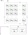
Fig. 2 embodies an example of the input device 100 of fig. 1 and illustrates the sensor electrodes 205 and the processing system 110. The sensor electrodes 205 are configured to sense one or more input objects (e.g., input object 140) in the sensing region 120. Each sensor electrode 205 may include one or more of the sensing elements described above. For clarity of illustration and description, fig. 2 presents regions of the sensor electrode 205 in a simple rectangular pattern, and does not show various other components connected to the sensor electrode 205 or within the sensor electrode 205.
An exemplary pattern of sensor electrodes 205 includes sensor electrodes 205 arranged in X columns and Y rows in a common planeX, Y(collectively sensor electrodes 205), where X and Y are positive integers, but one of X and Y may be zero. It is contemplated that the pattern of sensor electrodes 205 may include a plurality of sensor electrodes 205 having other configurations, such as a polar array, a repeating pattern, a non-uniform array, a single row or column, or other suitable arrangement. Further, as will be discussed in more detail below, the sensor electrodes 205 may be any shape, such as circular, rectangular, diamond, star, square, non-convex, non-concave, and the like. As shown here, the sensor electrodes 205 are coupled to the processing system 110 and are used to determine the presence (or absence) of input objects (e.g., input objects 140) and positional information in the sensing region 120.
The sensor electrodes 205 are ohmically isolated from each other. That is, one or more insulators separate the sensor electrodes and prevent them from electrically shorting to each other.
As illustrated in fig. 2, the processing system 110 includes a sensor driver 204 and a determination module 206, and the processing system 110 is coupled to a sensor electrode 205 via a trace 240. The processing system 110 is configured to operate the sensor electrodes 205 for capacitive sensing to detect the presence of one or more input objects (e.g., input object 140).
In one or more embodiments, the sensor driver 204 operates the one or more sensor electrodes 205 for absolute capacitive sensing to detect the presence of the input object 140. For example, the sensor driver 204 is configured to drive the sensor electrodes 205 using traces 240 with an absolute capacitive sensing signal and acquire a resulting signal from the driven sensor electrodes 205. In such embodiments, the resulting signal includes an effect corresponding to the absolute capacitive sensing signal. The absolute capacitive sensing signal may be a varying voltage signal. For example, the absolute capacitive sensing signal may vary between two or more voltages. In addition, the absolute capacitive sensing signal is periodic or aperiodic. Further, the absolute capacitive sensing signal may have one of a square waveform, a sinusoidal waveform, a trapezoidal waveform, or a triangular waveform, among others. The frequency of the absolute capacitive sensing signal may be in the range of about 100kHz to about 1 MHz. However, in other embodiments, frequencies less than 100kHz or frequencies greater than 1MHz may be utilized. Further, the absolute sense signal contains one or more sense bursts in one or more sense cycles. Each sense burst may include transitions from a first voltage to a second voltage and from the second voltage to the first voltage. However, in other embodiments, each sense burst may include transitions between more than two voltages.
In one or more embodiments, the sensor driver 204 is configured to operate the sensor electrodes 205 for absolute capacitive sensing by simultaneously driving two or more of the sensor electrodes 205 with absolute capacitive sensing signals. In such an embodiment, the resulting signals may be acquired from each driven sensor electrode 205 simultaneously. In one embodiment, the sensor driver 204 drives a first one or more of the sensor electrodes 205 with an absolute capacitive sensing signal during a first period of time and drives a second one or more of the sensor electrodes with an absolute capacitive sensing signal during a second period of time. The first and second periods of time may at least partially overlap or not overlap. In another embodiment, the sensor driver 204 drives each of the sensor electrodes 205 simultaneously during the same period.
In another embodiment, the sensor driver 204 operates the sensor electrodes 205 for transcapacitive sensing to detect the presence of the input object 140. That is, the sensor driver 204 may drive the first one or more sensor electrodes 205 with a transcapacitive sensing signal and receive a resulting signal using the second one or more sensor electrodes 205. The resulting signal includes an effect corresponding to the transcapacitive sense signal. The sensor electrodes driven with transcapacitive sensing signals are modulated relative to the sensor electrodes receiving the resulting signals. In one embodiment, both the sensor electrodes driven with the transcapacitive sense signal and the sensor electrodes receiving the resulting signal are modulated such that the sensor electrodes are modulated relative to each other. In another embodiment, the receiver electrodes are driven with a constant voltage signal while the sensor electrodes driven with a transcapacitive sense signal are driven with a transcapacitive sense signal.
The transcapacitive sense signal may be a varying voltage signal. For example, the transcapacitive sense signal may vary between two or more voltages. In addition, the transcapacitive sense signal is periodic or aperiodic. Further, the transcapacitive sense signal may have one of a square waveform, a sinusoidal waveform, a trapezoidal waveform, or a triangular waveform, among others. The frequency of the transcapacitive sense signal may be in the range of about 100kHz to about 1 MHz. However, in other embodiments, frequencies less than 100kHz or frequencies greater than 1MHz may be utilized. Further, the transcapacitive sense signal includes one or more sense bursts in one or more sense cycles. Each sense burst may include transitions from a first voltage to a second voltage and from the second voltage to the first voltage. In embodiments employing transcapacitive sense signals having more than two voltages, each sense burst may include more than two transitions. Further, the transcapacitive sense signal may be the same as or different from the absolute capacitive sense signal.
In some embodiments, the sensor driver 204 operates the sensor electrodes 205 for transcapacitive sensing by driving the sensor electrodes 205 across the capacitive sensing signal on a one-at-a-time basis. In such embodiments, the sensor driver 204 drives one sensor electrode 205 at a time with a transcapacitive sense signal. Further, the other sensor electrodes 205 may be driven with a substantially constant voltage.
Alternatively, the sensor driver 204 operates the sensor electrodes 205 for transcapacitive sensing by simultaneously driving multiple sensor electrodes 205 with transcapacitive sensing signals. In such embodiments, the sensor electrodes 205 are simultaneously driven with transcapacitive sensing signals. In one embodiment, two or more of the sensor electrodes 205 may be driven with the same transcapacitive sense signal at the same time. Driving two or more sensor electrodes 205 with the same transcapacitive sensing signal effectively results in a substantially larger sensor electrode (e.g., a group (gating) of sensor electrodes 205). In another embodiment, the sensor driver 204 may drive a first one or more of the sensor electrodes 205 with a first transcapacitive sensing signal and simultaneously drive a second one or more of the sensor electrodes with a second transcapacitive sensing signal different from the first transcapacitive sensing signal. Furthermore, the first and second transcapacitive sense signals may be based on different ones of a plurality of digital codes that enable independent determination of a combined effect on the resulting signals of the receiver electrodes.
In various embodiments, when a first one or more of the sensor electrodes 205 is driven with a transcapacitive sensing signal, a second one or more of the sensor electrodes may be operated singly or multiply to acquire a resulting signal.
The sensor driver 204 may be configured to operate the sensor electrodes 205 for absolute capacitive sensing and/or to operate the sensor electrodes 205 for transcapacitive sensing as described above. In one or more embodiments, the sensor driver 204 is configured to switch between operating the sensor electrodes 205 for absolute capacitive sensing and operating the sensor electrodes for transcapacitive sensing. Further, in various embodiments, the sensor driver 204 may be configured to selectively drive and receive a portion of the sensor electrodes 205. For example, sensor electrodes for performing absolute capacitive sensing and/or transcapacitive sensing may be selected based on, but not limited to, an application running on a host processor, a state of an input device, an operating mode of the sensing device, and a determined position of the input device. The host processor may be a central processing unit or any other processor of an electronic device. In various embodiments, the sensor driver 204 may operate the same sensor electrodes for absolute capacitive sensing and transcapacitive sensing. In one or more embodiments, the sensor driver 204 operates different sensor electrodes for absolute capacitive sensing and transcapacitive sensing.
The sensor driver 204 may operate the sensor electrodes 205 for absolute capacitive sensing and/or transcapacitive sensing during a capacitive frame. For example, a capacitive frame may correspond to operating each sensor electrode 205 for absolute capacitive sensing. Alternatively, a capacitive frame may correspond to operating each sensor electrode 205 to transcapacitive sensing. In another embodiment, a capacitive frame may correspond to operating each sensor electrode 205 for absolute capacitive sensing and transcapacitive sensing.
In some embodiments, one or more of the sensor electrodes 205 comprise one or more display electrodes used in updating the display of the display screen. In one or more embodiments, the display electrodes include one or more segments of a common voltage electrode (also referred to as a Vcom electrode), a source electrode, a gate electrode, an anode electrode, or a cathode electrode, among others. These display electrodes may be provided on a suitable display substrate. For example, in display screens such as in-plane switching (IPS) and plane-to-line switching (PLS) OLEDs, the display electrodes may be disposed on a transparent substrate, e.g., a glass substrate, Thin Film Transistor (TFT) glass, or any other transparent material. In other embodiments, display electrodes may be disposed on the bottom of the color filter glass in display screens such as Patterned Vertical Alignment (PVA) and multi-domain vertical alignment (MVA). In such embodiments, the electrodes used as both sensor electrodes and display electrodes may also be referred to as combined electrodes, as they perform multiple functions.
With continued reference to fig. 2, in various embodiments, the sensor driver 204 includes sensing circuitry configured to drive transcapacitive and absolute capacitive sensing signals onto the sensor electrodes 205 and receive resulting signals with the sensor electrodes 205 during periods in which input sensing is desired.
For example, in one or more embodiments, the sensor driver 204 includes a transmitter circuit configured to drive a transcapacitive sensing signal and/or an absolute capacitive sensing signal onto the sensor electrodes 205 during periods in which input sensing is desired.
Additionally or alternatively, the sensor driver 204 comprises a receiver circuit configured to receive a resulting signal with one or more of the sensor electrodes 205 when operating the sensor electrodes 205 for transcapacitive sensing and/or absolute capacitive sensing. In one or more embodiments, the sensor module includes a plurality of receivers, where each receiver may be an Analog Front End (AFE). Each receiver may be coupled to one or more sensor electrodes 205, respectively.
In one or more embodiments, the sensor driver 204 determines the location of input objects in the sensing region 120 based on the received resulting signals. In one or more embodiments, the sensor driver 204 provides the signal including information indicative of the resulting signal to another module or processor, such as a determination module of the processing system 110 or a processor (e.g., a host processor) of the electronic device, for determining positional information of the input object 140 in the sensing region 120. For example, in one embodiment, the sensor driver 204 may provide a signal indicative of the resulting signal to the determination module 206.
In embodiments where the sensor electrodes 205 are operated for absolute capacitive sensing, the determination module 206 determines a change in the absolute capacitance of the sensor electrodes 205 based on the resulting signals received by the sensor driver 204. In embodiments where the sensor electrode 205 is operated for transcapacitive sensing, the determination module 206 determines a change in the transcapacitive of the sensor electrode 205 based on the resulting signal received by the sensor driver 204. The determination module 206 may process the resulting signals or signals based on the resulting signals to determine one or more capacitive images from changes in absolute capacitive sensing and/or transcapacitive sensing. Further, the determination module 206 may determine positional information of the input object 140 from one or more capacitive images or from changes in absolute and/or transcapacitance.
In one or more embodiments, processing system 110 includes a display driver including display driver circuitry configured to drive display electrodes to update a display. The display driver may include a source driver circuit configured to drive a source electrode of the display device for display updating. The display driver may be included in the sensor driver 204 or separate from the sensor driver 204. In one embodiment, the processing system includes a first IC chip that includes at least a portion of the display driver and sensor driver 204. In another embodiment, the processing system 110 includes a first integrated controller including the display driver and a second integrated controller including at least a portion of the sensor driver 204.
In one or more embodiments, capacitive or input sensing and display updating may occur during periods that at least partially overlap. For example, when driving the display electrodes for display updating, the display electrodes may also be driven for capacitive sensing. Alternatively, the sensor electrodes 205 may be operated for transcapacitive sensing and/or absolute capacitive sensing, while the display electrodes are driven for display updating. The overlapping capacitive sensing and display update periods may include modulating reference voltage(s) of the display device and/or modulating one or more display electrodes of the display in a time period that at least partially overlaps with the time that the sensor electrodes are configured for capacitive sensing. In another embodiment, the capacitive sensing and display update may occur during non-overlapping periods (also referred to as non-display update periods). In various embodiments, the non-display update period may occur between display line update periods for two display lines of a display frame, and may be at least as long in time as the display update period. In such embodiments, the non-display update period may be referred to as a long horizontal blanking period, a long h-blanking period, or a distributed blanking period. In other embodiments, the non-display update period may include a horizontal blanking period and a vertical blanking period. The sensor driver 204 may be configured to drive the sensor electrodes for capacitive sensing during any one or more or any combination of different non-display update periods.
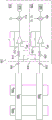
Fig. 3 and 4 illustrate a portion of the processing system 110 in two different modes of operation. For example, in fig. 3, processing system 110 is illustrated in a second mode in which receiver channels 310 and 320 are decoupled from one another. Further, in fig. 4, processing system 110 is illustrated in a first mode in which receiver channels 310 and 320 are coupled to each other.
FIG. 3 illustrates a portion of a processing system 110 in accordance with one or more embodiments. In particular, fig. 3 illustrates receiver channels 310 and 320 and switching mechanism 330. A switching mechanism 330 is coupled between the receiver channel 310 and an input of the receiver channel 320. Although fig. 3 illustrates two receiver channels and one switching mechanism, in one or more embodiments, processing system 110 may include more than two receiver channels and more than one switching mechanism. For example, the processing system 110 may include ten or more or one hundred or more receiver channels. Further, respective switching mechanisms are coupled to alternate pairs of receiver channels. For example, a first switching mechanism is coupled to the first receiver channel and the second receiver channel, and a second switching mechanism is coupled to the third receiver channel and the fourth receiver channel.
The integrator 312 may include an amplifier and a current conveyor 313. In other embodiments, a feedback capacitor and a feedback reset switch or resistor may be included within the integrator 312 instead of electricityA flow transmitter 313. Further, the inverting input of the amplifier of integrator 312 is coupled to a first end of resistor 315. A second end of resistor 315 is coupled to input terminal 340. The resistance value of resistor 315 may be in the range of about 100 ohms to about 10 kiloohms. In one embodiment, resistor 315 along with the capacitance of the associated sensor electrode 205 suppresses high frequency interference (e.g., GSM, etc.). The non-inverting input of the amplifier of the integrator 312 is configured to utilize the sense signal (V)TX) To modulate the sensor electrode 2051,2. For example, in the second mode, the non-inverting input of the amplifier of the integrator 312 is driven with the sense signal to modulate the sensor electrode 2051,2. Further, in the second mode, the sensor electrode 205 driven from the outside is driven via the inverting input of the amplifier of the integrator 3121,2A resulting signal is received.
A mixer 314 is coupled to the output of the integrator 312. In the second mode, the mixer 314 is configured to mix the output signal of the integrator 312 with the mixed signal S1And (4) mixing. The output of mixer 314 is provided to ADC 316. Mixed signal S1May be related to the sense signal (V)TX) Are identical in frequency and/or phase.
The integrator 322 includes an amplifier and a current conveyor 313. In other embodiments, a feedback capacitor and a feedback reset switch or resistor may be included within the integrator 322 in place of the current conveyor 323. Further, the inverting input of the amplifier of integrator 322 is coupled to a first end of a resistor 325. A second end of resistor 325 is coupled to input terminal 342. The resistance value of resistor 325 may be in the range of about 100 ohms to about 100 kiloohms. In one embodiment, resistor 315 is configured as a high frequency interference (e.g., GSM, etc.). Integrator 322 is configured to utilize the sense signal (V)TX) To modulate the sensor electrode 2052,2. For example, in the second mode, the non-inverting input of the amplifier of the integrator 322 is driven with the sense signal to modulate the sensor electrode 2052,2. Further, in the second mode, the inverting input of the amplifier via the integrator 322 is from the sensor electrode 205 that is driven2,2A resulting signal is received.
A mixer 324 is coupled to the output of the integrator 322. In the second mode, the mixer 324 is configured to mix the output signal of the integrator 322 with the mixed signal S1And (4) mixing. The output of mixer 324 is provided to ADC 326.
As discussed above, fig. 3 illustrates a second mode of the processing system 110. Further, as discussed above, in the second mode, the switching mechanism 330 decouples the receiver channel 310 from the receiver channel 320. The second mode corresponds to an input sensing mode. For example, during the second mode, the sensor electrode 2051,2And 2052,2Actively driven with a sense signal to detect the sensor electrode 2051,2And 2052,2A change in absolute capacitance of each of the electrodes.
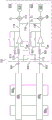
FIG. 4 illustrates the processing system 110 in a first mode in accordance with one or more embodiments. In response to receiver channels 310 and 320 being in the first mode, switching mechanism 330 couples an input of receiver channel 310 with an input of receiver channel 320. Thus, the combined resulting signal includes the slave sensor electrode 2051,2The resulting signals received and from the sensor electrodes 2052,2The resulting received signal, which is divided between receiver channels 310 and 320. Combination ofThe resulting signal of (a) includes the slave sensor electrode 2051,2The resulting signals received and from the sensor electrodes 2052,2The received result signal. The combined resulting signals include corresponding resulting signals received from two or more of the sensor electrodes 205. Alternatively, the combined resulting signals include corresponding resulting signals received from three or more of the sensor electrodes 205.
The resulting signals received by each receiver channel 310 and 320 correspond to sensor electrodes 2051,2And 2052,2About half of the total charge on. The resulting signals received by each receiver channel 310 and 320 are identical and correspond to equal portions of the combined resulting signal. In other embodiments, the resulting signals received by each receiver channel 310 and 320 are different and correspond to different portions of the combined resulting signal. For example, the resulting signals received by each receiver channel 310 and 320 differ due to differences in circuit characteristics between the receiver channels 310 and 320. The combined resulting signal corresponds to the sensor electrode 2051,2And 2052,2And the charge may be divided between each receiver channel 310 and 320.
In the first mode, the non-inverting input of each amplifier of each integrator 312 and 322 is driven with the reference voltage Vref. The reference voltage is a dc voltage. For example, the reference voltage may be a ground voltage. In other embodiments, the reference voltage may be a DC voltage other than a ground voltage. In addition, in the first mode, the mixer 324 mixes the output of the integrator 322 with the mixed signal S2And (4) mixing. Mixed signal S2May have a signal (V) corresponding to the sense signalTX) The same frequency. In addition, the mixed signal S2Differing in phase from the sense signal (V)TX). Furthermore, the mixed signal S2Is different from the mixed signal S1The phase of (c). For example, the mixed signal S2And mixed with signal S1Orthogonal (e.g., ninety degrees out of phase). Thus, receiver channel 310 determines the in-phase component of the corresponding resultant signal, and receiver channel 320 determines the quadrature component of the corresponding resultant signal. By determining modules206 may utilize the in-phase component and the quadrature component to determine a measure of interference. The measure of interference may correspond to a measure of an input object (e.g., input object 140) that is coupled to the interference. Input object coupling interference corresponds to interference coupled into the input device 100 when an input object is present within the sensing region (e.g., sensing region 120). Further, the in-phase component may be used to determine a measure of interference at the sense signal frequency, and the quadrature component may be used to determine a measure of interference that is ninety degrees out of phase with the sense signal frequency.
Fig. 5 illustrates another embodiment of a processing system 110. As compared to the embodiment of fig. 3, in the embodiment of fig. 5, each of receiver channels 310 and 320 is coupled to two or more sensor electrodes via switching mechanisms 360 and 370, respectively. Switching mechanism 360 selectively couples receiver channel 310 to input terminals 340a, 340b, and 340 c. Input terminals 340a, 340b, and 340c are coupled to sensor electrodes 205, respectively1,1、2051,2And 2051,3. In addition, a switching mechanism 370 selectively couples the receiver channel 320 to the input terminals 342a, 342b, 342 c. Input terminals 342a, 342b, and 342c are coupled to sensor electrodes 205, respectively2,1、2052,2And 2052,3. Switching mechanisms 360 and 370 may be included within processing system 110. Alternatively, the switching mechanisms 360 and 370 may be external to the processing system 110. In such embodiments, receiver channels 310 and 320 are each coupled to one or more input terminals 340 and 342, respectively, and input terminals 340 and 342 are coupled to switching mechanisms 360 and 370, respectively. Additionally, switching mechanisms 360 and 370 are coupled to sensor electrode 205 such that switching mechanisms 360 and 370 are disposed between sensor electrode 205 and input terminals 340, 342.
The switch mechanisms 360 and 370 may include one or more switches. In one embodiment, the number of switches of switching mechanisms 360 and 370 is at least as large as the number of sensor electrodes 205 to which each receiver channel 310, 320 is coupled. In various embodiments, switching mechanisms 360 and 370 may include one or more multiplexers.
The switching mechanism 360 may sense one at a time basisElectrode 205 of the device1,1、2051,2And 2051,3Coupled to a receiver channel 310. In addition, the switching mechanism 360 may simultaneously couple the sensor electrodes 2051,1、2051,2And 2051,3Are coupled to receiver channel 310. In addition, the switching mechanism 360 may simultaneously couple the sensor electrodes 2051,1、2051,2And 2051,3Each coupled to a receiver channel 310. For example, in the second mode, the switching mechanism 360 switches the sensor electrodes 205 one at a time on a one-at-a-time basis1,1、2051,2And 2051,3Coupled to a receiver channel 310. Further, during the first mode, the switching mechanism 360 simultaneously switches the sensor electrodes 2051,1、2051,2And 2051,3Coupled to a receiver channel 310.
The switching mechanism 370 may place the sensor electrodes 205 one at a time on a basis2,1、2052,2And 2052,3Coupled to the receiver channel 320. In addition, the switching mechanism 370 may simultaneously couple the sensor electrodes 2052,1、2052,2And 2052,3Are coupled to the receiver channel 320. In addition, the switching mechanism 370 may simultaneously couple the sensor electrodes 2052,1、2052,2And 2052,3Each coupled to a receiver channel 320. For example, in the second mode, the switching mechanism 370 switches the sensor electrodes 205 one at a time on a one-at-a-time basis2,1、2052,2And 2052,3Coupled to a receiver channel 310. Further, during the first mode, the switching mechanism 370 simultaneously switches the sensor electrodes 2052,1、2052,2And 2052,3Coupled to a receiver channel 310.
In the embodiment of fig. 5, the sensor electrodes coupled to each receiver channel 310 and 320 may correspond to orientations other than the orientation illustrated in fig. 5. For example, while each receiver channel is illustrated as being coupled to a common row of sensor electrodes, the receiver channels may be coupled to sensor electrodes in one or more rows and/or one or more columns. Further, the receiver channels may be coupled to one or more sensor electrodes that are not adjacent to each other.
Fig. 6 illustrates a processing system 602 coupled to a sensor electrode 605 in accordance with one or more embodiments. The processing system 602 is configured as a processing system similar to the processing system 110. For example, processing system 602 is configured to operate sensor electrodes 605 for capacitive sensing. Further, in one embodiment, the processing system 602 is configured to operate the sensor electrodes for transcapacitive sensing. For example, during the second mode, receiver channels 610 and 620 may be driven from sensor electrode 6051And 6052Receiving resulting signals, including signals corresponding to sensor electrodes 6053And 6054The effect of the up-driven transcapacitive sense signal.
The switching mechanism 630 is configured as a switching mechanism similar to the switching mechanism 330. For example, in the second mode, the switching mechanism decouples the receiver channel 610 from the receiver channel 620. In the first mode, the switching mechanism 630 couples the receiver channel 610 with the receiver channel 620. In the first mode, from sensor electrode 6051And 6052The combined resulting signal of (a) is output to the receiver channels 610 and 620. As described with reference to FIG. 4, in the first mode, portions of the combined result signal received by receiver channel 610 and portions of the combined result signal received by receiver channel 620May be the same or may be different from each other. For example, the portions of the combined result signal may differ based on the circuit characteristics of the receiver channels 610 and 620.
FIG. 7 illustrates a portion of a processing system 702 in accordance with one or more embodiments. Processing system 702 is configured as a processing system similar to processing systems 110 and 602. The processing system 702 includes a receiver channel 610, a receiver channel 620, and a switching mechanism 630. In addition, processing system 702 includes a switch 710 at the input of receiver channel 610, a switch 712 at the input of receiver channel 620, and a switch 716 between the outputs of integrators 612 and 622 and the inputs of mixers 614 and 624. Additionally, the processing system 702 includes a switch 718 at the output of the integrator 612 and a switch 720 at the output of the integrator 622.
In the first mode, the switches of the switching mechanism 630 are closed; receiver channel 610 is coupled with receiver channel 620 and switch 716 is closed. Further, switch 710 is closed and switch 712 is open. Additionally, switch 718 is closed and switch 720 is open. Thus, the integrator 622 may be bypassed such that the integrated signal received by the mixer 624 is provided by the integrator 612.
Further, in the first mode, the mixer 614 mixes the signal S1Is applied to the integrated signal output by the integrator 612 and the mixer 624 applies the mixing signal S1Is in phase quadrature with the mixed signal S2. Additionally, in the first mode, the integrated signals provided to mixers 614 and 624 are the same.
In the second mode, the switch of the switching mechanism 630 is open; the receiver channel 610 is decoupled from the receiver channel 620 and the switch 716 is opened. In addition, switches 710 and 712 are closed such that the inputs of receiver channels 610 and 620 are coupled to input terminals 640 and 642, respectively. Additionally, switches 718 and 720 are closed. Further, the mixers 614 and 624 mix the signal S respectively1The output signals applied to integrators 612 and 622.
In one or more embodiments, the processing system 110 of FIG. 3 can be replaced with the processing system 602 or 710.
FIG. 8 is a flow diagram of a method 800 for performing capacitive sensing in accordance with one or more embodiments. At operation 810, in a first mode, an input of a first receiver channel is coupled to an input of a second receiver channel. For example, referring to FIG. 4, switching mechanism 330 is closed and couples the input of receiver channel 310 to the input of receiver channel 320. Thus, from the sensor electrode 2051,2And 2052,2Are combined into a combined result signal. In other embodiments, as illustrated in fig. 5, the combined resulting signal is from the sensor electrode 2051,1、2051,2、2051,3、2052,1、2052,2And 2052,3And (4) receiving. A portion of the combined resultant signal is received by each receiver channel 310 and 320. In one embodiment, the portions of the combined result signal received by each receiver channel 310 and 320 are the same. Alternatively, the portion of the combined result signal received by each receiver channel 310 and 320 may be different. For example, the portion of the combined result signal received by each receiver channel 310 and 320 may differ based on the circuit characteristics of each receiver channel 310 and 320. For example, in one embodiment, receiver channel 310 may receive a greater portion of the combined result signal than receiver channel 320. In another embodiment, receiver channel 320 may receive a larger portion of the combined resultant signal than receiver channel 310. Further, as each receiver channel 310 and 320 receives a different portion of the combined resultant signal, it corresponds to the sensor electrode 205 received by each receiver channel 310 and 3201,2And 2052,2The amount of charge of (a) is different.
In the first mode, the sensor electrodes 205 are driven with a reference signal such that the corresponding resulting signal includes an effect corresponding to the disturbance. The interference may be coupled into the sensor electrode 205 via the input object 140. Driving sensor electrodes 205 with a reference signal1,2And 2052,2May include driving the non-inverting terminals of integrators 312 and 322 with a reference signal (e.g., Vref).
At operation 820A first output signal is generated when a receiver channel of the processing system is in a first mode. For example, receiver channel 310 may be configured by combining a first portion of the resulting signal with the mixed signal S1The mixing generates a first output signal. Combining a first part of the resulting signal with the sense signal (V)TX) Mixed signals S of the same phase and/or frequency1Mixing, generating an in-band component of the first portion of the combined result signal. Further, the first output signal may be generated by mixer 314. For example, in one embodiment, integrator 312 generates a first integrated signal from a first portion of the combined result signal. The mixer 314 mixes the first integrated signal with the mixed signal S1Mix to generate a first output signal.
At operation 830, a second output signal is generated when a receiver channel of the processing system is in a second mode. For example, the receiver channel 320 may be configured to combine the second portion of the resulting signal with the mixed signal S2The mixing generates a second output signal. Mixing of S2And the phase of the mixed signal S1Are in quadrature. Combining the second part of the resulting signal with the mixed signal S2The mixing generates quadrature components of the combined resultant signal. Further, the second output signal may be generated by mixer 324. For example, integrator 322 generates a second integrated signal from a second portion of the combined result signal. The mixer 324 mixes the second integrated signal with the mixed signal S2Mix to generate a second output signal.
At operation 840, interference information is determined. The determination module 206 determines a measurement of interference based on at least one of the first output signal and the second output signal. In one embodiment, the determination module 206 determines the measurement of the interference based on the first output signal or the second output signal. In another embodiment, the determination module 206 determines the measurement of the interference based on the first output signal and the second output signal. The determination module 206 receives a first output signal of the receiver channel 310 and a second output signal of the receiver channel 320. The first and second output signals may be processed by the ADC of each respective receiver channel before being passed to the determination module 206. DeterminingModule 206 determines the magnitude of the in-phase component of the combined result signal based on the first output signal and the magnitude of the quadrature component of the combined result signal based on the second output signal. The amplitude of the in-phase component may correspond to the mixed signal S1And the magnitude of the quadrature component may correspond to the mixed signal S2The amplitude of the disturbance at (c). In one embodiment, the signal S is mixed1And a mixed signal S2Ninety degrees out of phase with each other. Furthermore, the mixed signal S1Sensing signal (e.g., sensing signal V) driven on the sensor electrode in phase and frequencyTX) Similarly, to perform absolute capacitive sensing or transcapacitive sensing. Thus, the magnitude of the in-phase component corresponds to the magnitude of the disturbance at the sense signal, and the magnitude of the quadrature component corresponds to the magnitude of the disturbance ninety degrees out of phase with the sense signal.
The determination module 206 may alter the sense signal used to perform capacitive sensing (e.g., absolute capacitive sensing or transcapacitive sensing). For example, the determination module 206 may provide an indication to alter a sense signal used to perform absolute capacitive sensing based on measurements of the in-phase component and/or the quadrature component. Altering the sensing signal for capacitive sensing includes transitioning from driving the sensor electrode with the sensing signal having a first frequency to driving the sensor electrode with the sensing signal having a second frequency different from the first frequency.
In one embodiment, the determination module 206 compares the magnitude of the in-phase component and/or the quadrature component to a disturbance threshold to determine whether the disturbance threshold is exceeded. In response to determining that the magnitude of the in-band component and/or the magnitude of the quadrature component exceeds the interference threshold, the determination module 206 provides an indication to the sensor driver 204 to convert to a sensing signal having a different frequency.
At operation 850, when in the second mode, the input of the first receiver channel is decoupled from the input of the second receiver channel. For example, referring to FIG. 3, the switch of switching mechanism 330 is opened, decoupling the input of receiver channel 310 from the input of receiver channel 320.
At operation 860, generateA third output signal. For example, referring to fig. 3, by mixing the third result signal with the mixed signal S1Mixed to generate a third output signal from the receiver channel 310. Third resultant signal from sensor electrode 2051,2And receiving. To receive the third result signal, the sensor electrode 205 is driven with the sense signal1,2. For example, receiver channel 310 may modulate sensor electrode 205 with an absolute capacitive sensing signal1,2And from the sensor electrode 2051,2A first resulting signal is received. Modulating sensor electrodes 2051,2May include modulating a non-inverting input of the integrator 312 of the receiver channel 310. Alternatively, one or more sensor electrodes 205 may be driven with transcapacitive sense signals, while receiver channel 310 is driven from sensor electrodes 2051,2A third result signal is received.
The receiver channel 310 includes an integrator 312 that integrates the third resulting signal to generate an integrated signal. Furthermore, the mixer 314 mixes the integration signal with the mixed signal S1Mix to generate a third output signal.
At operation 870, a fourth output signal is generated. For example, referring to fig. 3, by mixing the fourth resulting signal with the mixed signal S1Mixed to generate a fourth output signal from the receiver channel 320. Slave sensor electrode 2052,2A fourth resulting signal is received. To receive the third result signal, the sensor electrode 205 is driven with the sense signal2,2. For example, the receiver channel 320 may modulate the sensor electrode 205 with an absolute capacitive sensing signal2,2And from the sensor electrode 2052,2A first resulting signal is received. Modulating sensor electrodes 2052,2May include a non-inverting input of an integrator 322 of the modulation receiver channel 320. Alternatively, one or more sensor electrodes 205 may be driven with transcapacitive sense signals, with receiver channels 320 from the sensor electrodes 2052,2A fourth resulting signal is received.
The receiver channel 320 includes an integrator 322 that integrates the fourth resultant signal to generate an integrated signal. Further, the mixer 324 mixes the integration signal with the mixed signal S1Mix to generate a fourth output signal.
In one or more embodiments, the determination module 206 may determine the location information based on the third output signal and the fourth output signal. The third and fourth output signals may be processed by the ADC of each respective receiver channel before being transmitted to the determination module 206. The determination module 206 baselines the third and fourth signals to generate corresponding baselined signals. The determination module 206 determines the sensor electrodes 205 from the baseline signal1,2And 2052,2A measurement of a change in capacitance of each of the plurality of sensors. Further, the determination module 206 compares the measurement of the change in capacitance to one or more thresholds to determine positional information of the input object (e.g., input object 140).
Thus, the embodiments and examples set forth herein are presented to best explain the embodiments in accordance with the present technology and its particular application and to thereby enable those skilled in the art to make and use the disclosure. Those skilled in the art, however, will recognize that the foregoing description and examples have been presented for the purpose of illustration and example only. The description as set forth is not intended to be exhaustive or to limit the disclosure to the precise form disclosed.
In view of the foregoing, the scope of the present disclosure is to be determined by the following claims.
Claims (20)
1. A processing system, comprising:
a first receiver channel configured to:
in a first mode, generating a first output signal by mixing a first portion of a combined resultant signal with a first mixed signal having a first phase, wherein the combined resultant signal comprises a first resultant signal received from a first sensor electrode and a second resultant signal received from a second sensor electrode;
a second receiver channel configured to:
generating a second output signal by mixing a second portion of the combined result signal with a second mixed signal having a second phase orthogonal to the first phase in the first mode, wherein the first portion of the combined result signal is different from the second portion of the combined result signal; and
a switch mechanism coupled to an input of the first receiver channel and an input of the second receiver channel, the switch mechanism configured to couple the input of the first receiver channel with the input of the second receiver channel in response to the first receiver channel and the second receiver channel being in the first mode.
2. The processing system of claim 1, wherein the first receiver channel and the second receiver channel are configured to generate the first output signal and the second output signal simultaneously.
3. The processing system of claim 1, further comprising:
a determination module configured to determine a measure of interference based on at least one of the first output signal and the second output signal.
4. The processing system of claim 1, wherein the first receiver channel, when in the second mode, is further configured to generate a third output signal by mixing a third resulting signal with the first mixed signal, the third resulting signal received from the first sensor electrode,
the second receiver channel, when in the second mode, is further configured to generate a fourth output signal by mixing a fourth resultant signal with the first mixed signal, the fourth resultant signal received from the second sensor electrode, and
the switch mechanism is further configured to decouple the input of the first receiver channel from the input of the second receiver channel in response to the first receiver channel and the second receiver channel being in the second mode.
5. The processing system of claim 4, further comprising:
a determination module configured to determine positional information of an input object based on at least one of the third output signal and the fourth output signal.
6. The processing system of claim 1, wherein the first receiver channel comprises:
a first resistor coupled to a first input terminal of the processing system;
a first integrator having an input coupled to the first resistor and configured to integrate the first portion of the combined result signal; and
a first mixer coupled to an output of the first integrator and configured to generate the first output signal, wherein the second receiver channel comprises:
a second resistor coupled to a second input terminal of the processing system;
a second integrator having an input coupled to the second resistor and configured to integrate the second portion of the combined result signal; and
a second mixer coupled to an output of the second integrator and configured to generate the second output signal, an
Wherein the switch mechanism is coupled to the input of the first receiver channel between the first input terminal and the first resistor and to the input of the second receiver channel between the second input terminal and the second resistor.
7. The processing system of claim 1, wherein the first portion of the combined result signal is greater than the second portion of the combined result signal, or the second portion of the combined result signal is greater than the first portion of the combined result signal.
8. An input device, comprising:
a plurality of sensor electrodes including a first sensor electrode and a second sensor electrode; and
a processing system coupled to the plurality of sensor electrodes, the processing system comprising:
a first receiver channel configured to:
generating a first output signal by mixing a first portion of a combined resultant signal with a first mixed signal having a first phase while in a first mode, wherein the combined resultant signal includes a first resultant signal received from the first sensor electrode and a second resultant signal received from the second sensor electrode;
a second receiver channel configured to:
generating a second output signal by mixing a second portion of the combined result signal with a second mixed signal having a second phase orthogonal to the first phase, while in the first mode, wherein the first portion of the combined result signal is different from the second portion of the combined result signal; and
a first switching mechanism coupled to an input of the first receiver channel and an input of the second receiver channel, the first switching mechanism configured to couple the input of the first receiver channel with the input of the second receiver channel in response to the first receiver channel and the second receiver channel being in the first mode.
9. The input device of claim 8, wherein the first receiver channel and the second receiver channel are configured to generate the first output signal and the second output signal simultaneously.
10. The input device of claim 9, wherein the processing system is configured to determine a measure of interference based on at least one of the first output signal and the second output signal.
11. The input device of claim 8, wherein the first receiver channel, when in a second mode, is further configured to generate a third output signal by mixing a third resulting signal with the first mixed signal, the third resulting signal received from the first sensor electrode,
the second receiver channel, when in the second mode, is further configured to generate a fourth output signal by mixing a fourth resultant signal with the first mixed signal, the fourth resultant signal received from the second sensor electrode, and
the first switching mechanism is configured to decouple the input of the first receiver channel from the input of the second receiver channel in response to the first receiver channel and the second receiver channel being in the second mode.
12. The input device of claim 11, wherein the processing system is configured to determine positional information of an input object based on at least one of the third output signal and the fourth output signal.
13. The input device of claim 8, wherein the first receiver channel comprises:
a first resistor coupled to a first input terminal of the processing system;
a first integrator having an input coupled to the first resistor, the first integrator configured to integrate the first portion of the combined result signal; and
a first mixer coupled to an output of the first integrator, the first mixer configured to generate the first output signal, wherein the second receiver channel comprises:
a second resistor coupled to a second input terminal of the processing system;
a second integrator having an input coupled to the second resistor, the second integrator configured to integrate the second portion of the combined result signal; and
a second mixer coupled to an output of the second integrator, the second mixer configured to generate the second output signal, an
Wherein the first switching mechanism is coupled to the input of the first receiver channel between the first input terminal and the first resistor and to the input of the second receiver channel between the second input terminal and the second resistor.
14. The input device of claim 8, wherein the processing system further comprises a second switching mechanism coupled between an input terminal of the processing system and the input of the first receiver channel, the second switching mechanism configured to couple the input terminal with the input of the first receiver channel in response to the first receiver channel being in the first mode.
15. The input device of claim 8, wherein the first portion of the combined result signal is greater than the second portion of the combined result signal or the second portion of the combined result signal is greater than the first portion of the combined result signal.
16. A method of capacitive sensing, the method comprising:
in a first mode, coupling an input of a first receiver channel with an input of a second receiver channel;
generating, by the first receiver channel and while in the first mode, a first output signal by mixing a first portion of a combined resultant signal with a first mixed signal having a first phase, wherein the combined resultant signal includes a first resultant signal received from a first sensor electrode and a second resultant signal received from a second sensor electrode; and
generating, by the second receiver channel and while in the first mode, a second output signal by mixing a second portion of the combined result signal with a second mixed signal having a second phase orthogonal to the first mixed signal, wherein the first portion of the combined result signal is different from the second portion of the combined result signal.
17. The method of claim 16, wherein the first output signal and the second output signal are generated simultaneously.
18. The method of claim 16, further comprising:
determining a measure of interference based on at least one of the first output signal and the second output signal.
19. The method of claim 16, further comprising:
in a second mode, decoupling the input of the first receiver channel from the input of the second receiver channel;
generating a third output signal by mixing a third resulting signal with the first mixed signal through the first receiver channel while in the second mode, wherein the third resulting signal is received from the first sensor electrode;
generating, by the second receiver channel while in the second mode, a fourth output signal by mixing a fourth resultant signal with the first mixed signal, wherein the fourth resultant signal is received from the second sensor electrode; and
determining position information of an input object based on at least one of the third output signal and the fourth output signal.
20. The method of claim 16, wherein the first portion of the combined result signal is greater than the second portion of the combined result signal or the second portion of the combined result signal is greater than the first portion of the combined result signal.
Applications Claiming Priority (2)
| Application Number | Priority Date | Filing Date | Title |
|---|---|---|---|
| US16/821599 | 2020-03-17 | ||
| US16/821,599 US11397487B2 (en) | 2020-03-17 | 2020-03-17 | Re-configurable receiver channels for a sensing device |
Publications (1)
| Publication Number | Publication Date |
|---|---|
| CN113407052A true CN113407052A (en) | 2021-09-17 |
Family
ID=77677610
Family Applications (1)
| Application Number | Title | Priority Date | Filing Date |
|---|---|---|---|
| CN202110279407.2A Pending CN113407052A (en) | 2020-03-17 | 2021-03-16 | Reconfigurable receiver channel for sensing devices |
Country Status (3)
| Country | Link |
|---|---|
| US (1) | US11397487B2 (en) |
| JP (1) | JP2021149962A (en) |
| CN (1) | CN113407052A (en) |
Family Cites Families (20)
| Publication number | Priority date | Publication date | Assignee | Title |
|---|---|---|---|---|
| GB2214374A (en) * | 1988-01-06 | 1989-08-31 | Philips Electronic Associated | Ssb signal generator |
| DE69324067T2 (en) * | 1992-06-08 | 1999-07-15 | Synaptics Inc | Object position detector |
| US5880411A (en) * | 1992-06-08 | 1999-03-09 | Synaptics, Incorporated | Object position detector with edge motion feature and gesture recognition |
| TW274598B (en) * | 1994-11-15 | 1996-04-21 | Alps Electric Co Ltd | Coordinate input device for pen of finger tip |
| JP4487955B2 (en) * | 2006-03-01 | 2010-06-23 | ソニー株式会社 | Wireless communication apparatus and method |
| US8730204B2 (en) * | 2010-09-16 | 2014-05-20 | Synaptics Incorporated | Systems and methods for signaling and interference detection in sensor devices |
| WO2012148539A1 (en) * | 2011-02-25 | 2012-11-01 | Maxim Integrated Products, Inc | Capacitive touch sense architecture |
| US9086439B2 (en) * | 2011-02-25 | 2015-07-21 | Maxim Integrated Products, Inc. | Circuits, devices and methods having pipelined capacitance sensing |
| US8729911B2 (en) * | 2011-04-19 | 2014-05-20 | Cypress Semiconductor Corporation | Usage of weighting matrices in multi-phase scanning modes |
| US8766949B2 (en) * | 2011-12-22 | 2014-07-01 | Synaptics Incorporated | Systems and methods for determining user input using simultaneous transmission from multiple electrodes |
| US9436325B2 (en) * | 2013-12-20 | 2016-09-06 | Synaptics Incorporated | Active pen for matrix sensor |
| US9389742B2 (en) * | 2014-12-10 | 2016-07-12 | Pixart Imaging Inc. | Capacitive touch device, capacitive communication device and communication system |
| US10126884B2 (en) * | 2014-12-22 | 2018-11-13 | Synaptics Incorporated | Asynchronous interference detection in a capacitive sensing system |
| US10025428B2 (en) * | 2015-11-19 | 2018-07-17 | Synaptics Incorporated | Method and apparatus for improving capacitive sensing detection |
| US10353518B2 (en) * | 2016-10-14 | 2019-07-16 | Synaptics Incorporated | Touch controller with signal combining and simultaneous I/Q demodulation |
| US10133435B2 (en) * | 2017-01-03 | 2018-11-20 | Synaptics Incorporated | Reduced capacitive baseline shift via switching elements |
| US10162462B2 (en) * | 2017-05-01 | 2018-12-25 | Synaptics Incorporated | Integrating capacitive sensing with an optical sensor |
| US10203809B2 (en) | 2017-05-25 | 2019-02-12 | Synaptics Incorporated | Interference detection |
| US11119606B2 (en) * | 2019-08-20 | 2021-09-14 | Synaptics Incorporated | Background capacitance compensation |
| US10928944B1 (en) * | 2019-11-22 | 2021-02-23 | Synaptics Incorporated | Device and method for proximity sensing on an input device |
-
2020
- 2020-03-17 US US16/821,599 patent/US11397487B2/en active Active
-
2021
- 2021-03-03 JP JP2021033306A patent/JP2021149962A/en active Pending
- 2021-03-16 CN CN202110279407.2A patent/CN113407052A/en active Pending
Also Published As
| Publication number | Publication date |
|---|---|
| US20210294449A1 (en) | 2021-09-23 |
| JP2021149962A (en) | 2021-09-27 |
| US11397487B2 (en) | 2022-07-26 |
Similar Documents
| Publication | Publication Date | Title |
|---|---|---|
| US10126884B2 (en) | Asynchronous interference detection in a capacitive sensing system | |
| CN107148608B (en) | Apparatus and method for force and proximity sensing with intermediate shield electrode layers | |
| US9075488B2 (en) | Virtual geometries for integrated display and sensing devices | |
| US9600121B2 (en) | Driving sensor electrodes for noise measurement | |
| US10228797B2 (en) | Continuous time anti-alias filter for capacitive touch sensing | |
| US9329731B2 (en) | Routing trace compensation | |
| WO2015048482A1 (en) | Using a printed circuit to offset charge during capacitive sensing | |
| US9606670B2 (en) | Real-time spectral noise monitoring for proximity sensing device | |
| US9946404B1 (en) | LED screen noise sensing for discreet capacitive sensors | |
| US9471173B2 (en) | Capacitive input sensing in the presence of a uniform conductor | |
| US9811205B2 (en) | Variable time anti-aliasing filter | |
| US20160183382A1 (en) | Capacitive image sensor with selectable function electrodes | |
| US10175827B2 (en) | Detecting an active pen using a capacitive sensing device | |
| US20150378498A1 (en) | Hybrid capacitive sensor device | |
| CN105468215B (en) | Current feedback techniques for capacitive sensing | |
| US20210157434A1 (en) | Device and method for proximity sensing on an input device | |
| US9760205B2 (en) | Interference mitigation in a capacitive sensing device | |
| US9268435B2 (en) | Single layer capacitive sensor and capacitive sensing input device | |
| CN109313521B (en) | Calibrating continuous-time receivers for capacitive sensing | |
| CN109032436B (en) | Interference suppression and clock jitter for continuous time receivers for capacitive sensing | |
| CN105760027B (en) | Switched capacitor technology for input sensing | |
| US11397487B2 (en) | Re-configurable receiver channels for a sensing device | |
| US20150091840A1 (en) | Far-field sensing with a display device having an integrated sensing device | |
| US10055045B2 (en) | Current feedback digital charge accumulator | |
| US11144162B1 (en) | Device and method for sensor electrode testing |
Legal Events
| Date | Code | Title | Description |
|---|---|---|---|
| PB01 | Publication | ||
| PB01 | Publication | ||
| SE01 | Entry into force of request for substantive examination | ||
| SE01 | Entry into force of request for substantive examination |