CN112772004A - Electrical device, interlayer sheet comprising electrical device and method for manufacturing electrical device and interlayer sheet - Google Patents
Electrical device, interlayer sheet comprising electrical device and method for manufacturing electrical device and interlayer sheet Download PDFInfo
- Publication number
- CN112772004A CN112772004A CN201980064632.5A CN201980064632A CN112772004A CN 112772004 A CN112772004 A CN 112772004A CN 201980064632 A CN201980064632 A CN 201980064632A CN 112772004 A CN112772004 A CN 112772004A
- Authority
- CN
- China
- Prior art keywords
- major surface
- electrical
- layer
- interlayer material
- flexible circuit
- Prior art date
- Legal status (The legal status is an assumption and is not a legal conclusion. Google has not performed a legal analysis and makes no representation as to the accuracy of the status listed.)
- Pending
Links
Images


Classifications
-
- H—ELECTRICITY
- H05—ELECTRIC TECHNIQUES NOT OTHERWISE PROVIDED FOR
- H05K—PRINTED CIRCUITS; CASINGS OR CONSTRUCTIONAL DETAILS OF ELECTRIC APPARATUS; MANUFACTURE OF ASSEMBLAGES OF ELECTRICAL COMPONENTS
- H05K1/00—Printed circuits
- H05K1/18—Printed circuits structurally associated with non-printed electric components
- H05K1/182—Printed circuits structurally associated with non-printed electric components associated with components mounted in the printed circuit board, e.g. insert mounted components [IMC]
- H05K1/185—Components encapsulated in the insulating substrate of the printed circuit or incorporated in internal layers of a multilayer circuit
- H05K1/186—Components encapsulated in the insulating substrate of the printed circuit or incorporated in internal layers of a multilayer circuit manufactured by mounting on or connecting to patterned circuits before or during embedding
- H05K1/187—Components encapsulated in the insulating substrate of the printed circuit or incorporated in internal layers of a multilayer circuit manufactured by mounting on or connecting to patterned circuits before or during embedding the patterned circuits being prefabricated circuits, which are not yet attached to a permanent insulating substrate, e.g. on a temporary carrier
-
- H—ELECTRICITY
- H05—ELECTRIC TECHNIQUES NOT OTHERWISE PROVIDED FOR
- H05B—ELECTRIC HEATING; ELECTRIC LIGHT SOURCES NOT OTHERWISE PROVIDED FOR; CIRCUIT ARRANGEMENTS FOR ELECTRIC LIGHT SOURCES, IN GENERAL
- H05B3/00—Ohmic-resistance heating
- H05B3/84—Heating arrangements specially adapted for transparent or reflecting areas, e.g. for demisting or de-icing windows, mirrors or vehicle windshields
-
- B—PERFORMING OPERATIONS; TRANSPORTING
- B32—LAYERED PRODUCTS
- B32B—LAYERED PRODUCTS, i.e. PRODUCTS BUILT-UP OF STRATA OF FLAT OR NON-FLAT, e.g. CELLULAR OR HONEYCOMB, FORM
- B32B17/00—Layered products essentially comprising sheet glass, or glass, slag, or like fibres
- B32B17/06—Layered products essentially comprising sheet glass, or glass, slag, or like fibres comprising glass as the main or only constituent of a layer, next to another layer of a specific material
- B32B17/10—Layered products essentially comprising sheet glass, or glass, slag, or like fibres comprising glass as the main or only constituent of a layer, next to another layer of a specific material of synthetic resin
- B32B17/10005—Layered products essentially comprising sheet glass, or glass, slag, or like fibres comprising glass as the main or only constituent of a layer, next to another layer of a specific material of synthetic resin laminated safety glass or glazing
- B32B17/10009—Layered products essentially comprising sheet glass, or glass, slag, or like fibres comprising glass as the main or only constituent of a layer, next to another layer of a specific material of synthetic resin laminated safety glass or glazing characterized by the number, the constitution or treatment of glass sheets
- B32B17/10036—Layered products essentially comprising sheet glass, or glass, slag, or like fibres comprising glass as the main or only constituent of a layer, next to another layer of a specific material of synthetic resin laminated safety glass or glazing characterized by the number, the constitution or treatment of glass sheets comprising two outer glass sheets
-
- B—PERFORMING OPERATIONS; TRANSPORTING
- B32—LAYERED PRODUCTS
- B32B—LAYERED PRODUCTS, i.e. PRODUCTS BUILT-UP OF STRATA OF FLAT OR NON-FLAT, e.g. CELLULAR OR HONEYCOMB, FORM
- B32B17/00—Layered products essentially comprising sheet glass, or glass, slag, or like fibres
- B32B17/06—Layered products essentially comprising sheet glass, or glass, slag, or like fibres comprising glass as the main or only constituent of a layer, next to another layer of a specific material
- B32B17/10—Layered products essentially comprising sheet glass, or glass, slag, or like fibres comprising glass as the main or only constituent of a layer, next to another layer of a specific material of synthetic resin
- B32B17/10005—Layered products essentially comprising sheet glass, or glass, slag, or like fibres comprising glass as the main or only constituent of a layer, next to another layer of a specific material of synthetic resin laminated safety glass or glazing
- B32B17/10165—Functional features of the laminated safety glass or glazing
- B32B17/10541—Functional features of the laminated safety glass or glazing comprising a light source or a light guide
-
- B—PERFORMING OPERATIONS; TRANSPORTING
- B32—LAYERED PRODUCTS
- B32B—LAYERED PRODUCTS, i.e. PRODUCTS BUILT-UP OF STRATA OF FLAT OR NON-FLAT, e.g. CELLULAR OR HONEYCOMB, FORM
- B32B17/00—Layered products essentially comprising sheet glass, or glass, slag, or like fibres
- B32B17/06—Layered products essentially comprising sheet glass, or glass, slag, or like fibres comprising glass as the main or only constituent of a layer, next to another layer of a specific material
- B32B17/10—Layered products essentially comprising sheet glass, or glass, slag, or like fibres comprising glass as the main or only constituent of a layer, next to another layer of a specific material of synthetic resin
- B32B17/10005—Layered products essentially comprising sheet glass, or glass, slag, or like fibres comprising glass as the main or only constituent of a layer, next to another layer of a specific material of synthetic resin laminated safety glass or glazing
- B32B17/1055—Layered products essentially comprising sheet glass, or glass, slag, or like fibres comprising glass as the main or only constituent of a layer, next to another layer of a specific material of synthetic resin laminated safety glass or glazing characterized by the resin layer, i.e. interlayer
- B32B17/10761—Layered products essentially comprising sheet glass, or glass, slag, or like fibres comprising glass as the main or only constituent of a layer, next to another layer of a specific material of synthetic resin laminated safety glass or glazing characterized by the resin layer, i.e. interlayer containing vinyl acetal
-
- B—PERFORMING OPERATIONS; TRANSPORTING
- B32—LAYERED PRODUCTS
- B32B—LAYERED PRODUCTS, i.e. PRODUCTS BUILT-UP OF STRATA OF FLAT OR NON-FLAT, e.g. CELLULAR OR HONEYCOMB, FORM
- B32B17/00—Layered products essentially comprising sheet glass, or glass, slag, or like fibres
- B32B17/06—Layered products essentially comprising sheet glass, or glass, slag, or like fibres comprising glass as the main or only constituent of a layer, next to another layer of a specific material
- B32B17/10—Layered products essentially comprising sheet glass, or glass, slag, or like fibres comprising glass as the main or only constituent of a layer, next to another layer of a specific material of synthetic resin
- B32B17/10005—Layered products essentially comprising sheet glass, or glass, slag, or like fibres comprising glass as the main or only constituent of a layer, next to another layer of a specific material of synthetic resin laminated safety glass or glazing
- B32B17/1055—Layered products essentially comprising sheet glass, or glass, slag, or like fibres comprising glass as the main or only constituent of a layer, next to another layer of a specific material of synthetic resin laminated safety glass or glazing characterized by the resin layer, i.e. interlayer
- B32B17/1077—Layered products essentially comprising sheet glass, or glass, slag, or like fibres comprising glass as the main or only constituent of a layer, next to another layer of a specific material of synthetic resin laminated safety glass or glazing characterized by the resin layer, i.e. interlayer containing polyurethane
-
- B—PERFORMING OPERATIONS; TRANSPORTING
- B32—LAYERED PRODUCTS
- B32B—LAYERED PRODUCTS, i.e. PRODUCTS BUILT-UP OF STRATA OF FLAT OR NON-FLAT, e.g. CELLULAR OR HONEYCOMB, FORM
- B32B17/00—Layered products essentially comprising sheet glass, or glass, slag, or like fibres
- B32B17/06—Layered products essentially comprising sheet glass, or glass, slag, or like fibres comprising glass as the main or only constituent of a layer, next to another layer of a specific material
- B32B17/10—Layered products essentially comprising sheet glass, or glass, slag, or like fibres comprising glass as the main or only constituent of a layer, next to another layer of a specific material of synthetic resin
- B32B17/10005—Layered products essentially comprising sheet glass, or glass, slag, or like fibres comprising glass as the main or only constituent of a layer, next to another layer of a specific material of synthetic resin laminated safety glass or glazing
- B32B17/1055—Layered products essentially comprising sheet glass, or glass, slag, or like fibres comprising glass as the main or only constituent of a layer, next to another layer of a specific material of synthetic resin laminated safety glass or glazing characterized by the resin layer, i.e. interlayer
- B32B17/10788—Layered products essentially comprising sheet glass, or glass, slag, or like fibres comprising glass as the main or only constituent of a layer, next to another layer of a specific material of synthetic resin laminated safety glass or glazing characterized by the resin layer, i.e. interlayer containing ethylene vinylacetate
-
- B—PERFORMING OPERATIONS; TRANSPORTING
- B32—LAYERED PRODUCTS
- B32B—LAYERED PRODUCTS, i.e. PRODUCTS BUILT-UP OF STRATA OF FLAT OR NON-FLAT, e.g. CELLULAR OR HONEYCOMB, FORM
- B32B17/00—Layered products essentially comprising sheet glass, or glass, slag, or like fibres
- B32B17/06—Layered products essentially comprising sheet glass, or glass, slag, or like fibres comprising glass as the main or only constituent of a layer, next to another layer of a specific material
- B32B17/10—Layered products essentially comprising sheet glass, or glass, slag, or like fibres comprising glass as the main or only constituent of a layer, next to another layer of a specific material of synthetic resin
- B32B17/10005—Layered products essentially comprising sheet glass, or glass, slag, or like fibres comprising glass as the main or only constituent of a layer, next to another layer of a specific material of synthetic resin laminated safety glass or glazing
- B32B17/10807—Making laminated safety glass or glazing; Apparatus therefor
- B32B17/10899—Making laminated safety glass or glazing; Apparatus therefor by introducing interlayers of synthetic resin
- B32B17/10935—Making laminated safety glass or glazing; Apparatus therefor by introducing interlayers of synthetic resin as a preformed layer, e.g. formed by extrusion
-
- B—PERFORMING OPERATIONS; TRANSPORTING
- B32—LAYERED PRODUCTS
- B32B—LAYERED PRODUCTS, i.e. PRODUCTS BUILT-UP OF STRATA OF FLAT OR NON-FLAT, e.g. CELLULAR OR HONEYCOMB, FORM
- B32B27/00—Layered products comprising a layer of synthetic resin
- B32B27/06—Layered products comprising a layer of synthetic resin as the main or only constituent of a layer, which is next to another layer of the same or of a different material
- B32B27/08—Layered products comprising a layer of synthetic resin as the main or only constituent of a layer, which is next to another layer of the same or of a different material of synthetic resin
-
- B—PERFORMING OPERATIONS; TRANSPORTING
- B32—LAYERED PRODUCTS
- B32B—LAYERED PRODUCTS, i.e. PRODUCTS BUILT-UP OF STRATA OF FLAT OR NON-FLAT, e.g. CELLULAR OR HONEYCOMB, FORM
- B32B3/00—Layered products comprising a layer with external or internal discontinuities or unevennesses, or a layer of non-planar form; Layered products having particular features of form
- B32B3/26—Layered products comprising a layer with external or internal discontinuities or unevennesses, or a layer of non-planar form; Layered products having particular features of form characterised by a particular shape of the outline of the cross-section of a continuous layer; characterised by a layer with cavities or internal voids ; characterised by an apertured layer
- B32B3/266—Layered products comprising a layer with external or internal discontinuities or unevennesses, or a layer of non-planar form; Layered products having particular features of form characterised by a particular shape of the outline of the cross-section of a continuous layer; characterised by a layer with cavities or internal voids ; characterised by an apertured layer characterised by an apertured layer, the apertures going through the whole thickness of the layer, e.g. expanded metal, perforated layer, slit layer regular cells B32B3/12
-
- H—ELECTRICITY
- H05—ELECTRIC TECHNIQUES NOT OTHERWISE PROVIDED FOR
- H05K—PRINTED CIRCUITS; CASINGS OR CONSTRUCTIONAL DETAILS OF ELECTRIC APPARATUS; MANUFACTURE OF ASSEMBLAGES OF ELECTRICAL COMPONENTS
- H05K1/00—Printed circuits
- H05K1/02—Details
- H05K1/14—Structural association of two or more printed circuits
- H05K1/147—Structural association of two or more printed circuits at least one of the printed circuits being bent or folded, e.g. by using a flexible printed circuit
-
- H—ELECTRICITY
- H05—ELECTRIC TECHNIQUES NOT OTHERWISE PROVIDED FOR
- H05K—PRINTED CIRCUITS; CASINGS OR CONSTRUCTIONAL DETAILS OF ELECTRIC APPARATUS; MANUFACTURE OF ASSEMBLAGES OF ELECTRICAL COMPONENTS
- H05K3/00—Apparatus or processes for manufacturing printed circuits
- H05K3/0058—Laminating printed circuit boards onto other substrates, e.g. metallic substrates
-
- H—ELECTRICITY
- H05—ELECTRIC TECHNIQUES NOT OTHERWISE PROVIDED FOR
- H05K—PRINTED CIRCUITS; CASINGS OR CONSTRUCTIONAL DETAILS OF ELECTRIC APPARATUS; MANUFACTURE OF ASSEMBLAGES OF ELECTRICAL COMPONENTS
- H05K3/00—Apparatus or processes for manufacturing printed circuits
- H05K3/0097—Processing two or more printed circuits simultaneously, e.g. made from a common substrate, or temporarily stacked circuit boards
-
- H—ELECTRICITY
- H05—ELECTRIC TECHNIQUES NOT OTHERWISE PROVIDED FOR
- H05K—PRINTED CIRCUITS; CASINGS OR CONSTRUCTIONAL DETAILS OF ELECTRIC APPARATUS; MANUFACTURE OF ASSEMBLAGES OF ELECTRICAL COMPONENTS
- H05K3/00—Apparatus or processes for manufacturing printed circuits
- H05K3/22—Secondary treatment of printed circuits
- H05K3/28—Applying non-metallic protective coatings
- H05K3/284—Applying non-metallic protective coatings for encapsulating mounted components
-
- B—PERFORMING OPERATIONS; TRANSPORTING
- B32—LAYERED PRODUCTS
- B32B—LAYERED PRODUCTS, i.e. PRODUCTS BUILT-UP OF STRATA OF FLAT OR NON-FLAT, e.g. CELLULAR OR HONEYCOMB, FORM
- B32B2250/00—Layers arrangement
- B32B2250/02—2 layers
-
- B—PERFORMING OPERATIONS; TRANSPORTING
- B32—LAYERED PRODUCTS
- B32B—LAYERED PRODUCTS, i.e. PRODUCTS BUILT-UP OF STRATA OF FLAT OR NON-FLAT, e.g. CELLULAR OR HONEYCOMB, FORM
- B32B2250/00—Layers arrangement
- B32B2250/03—3 layers
-
- B—PERFORMING OPERATIONS; TRANSPORTING
- B32—LAYERED PRODUCTS
- B32B—LAYERED PRODUCTS, i.e. PRODUCTS BUILT-UP OF STRATA OF FLAT OR NON-FLAT, e.g. CELLULAR OR HONEYCOMB, FORM
- B32B2419/00—Buildings or parts thereof
-
- B—PERFORMING OPERATIONS; TRANSPORTING
- B32—LAYERED PRODUCTS
- B32B—LAYERED PRODUCTS, i.e. PRODUCTS BUILT-UP OF STRATA OF FLAT OR NON-FLAT, e.g. CELLULAR OR HONEYCOMB, FORM
- B32B2457/00—Electrical equipment
-
- B—PERFORMING OPERATIONS; TRANSPORTING
- B32—LAYERED PRODUCTS
- B32B—LAYERED PRODUCTS, i.e. PRODUCTS BUILT-UP OF STRATA OF FLAT OR NON-FLAT, e.g. CELLULAR OR HONEYCOMB, FORM
- B32B2457/00—Electrical equipment
- B32B2457/08—PCBs, i.e. printed circuit boards
-
- B—PERFORMING OPERATIONS; TRANSPORTING
- B32—LAYERED PRODUCTS
- B32B—LAYERED PRODUCTS, i.e. PRODUCTS BUILT-UP OF STRATA OF FLAT OR NON-FLAT, e.g. CELLULAR OR HONEYCOMB, FORM
- B32B2605/00—Vehicles
- B32B2605/08—Cars
-
- H—ELECTRICITY
- H05—ELECTRIC TECHNIQUES NOT OTHERWISE PROVIDED FOR
- H05K—PRINTED CIRCUITS; CASINGS OR CONSTRUCTIONAL DETAILS OF ELECTRIC APPARATUS; MANUFACTURE OF ASSEMBLAGES OF ELECTRICAL COMPONENTS
- H05K2201/00—Indexing scheme relating to printed circuits covered by H05K1/00
- H05K2201/09—Shape and layout
- H05K2201/09209—Shape and layout details of conductors
- H05K2201/09654—Shape and layout details of conductors covering at least two types of conductors provided for in H05K2201/09218 - H05K2201/095
- H05K2201/09754—Connector integrally incorporated in the PCB or in housing
-
- H—ELECTRICITY
- H05—ELECTRIC TECHNIQUES NOT OTHERWISE PROVIDED FOR
- H05K—PRINTED CIRCUITS; CASINGS OR CONSTRUCTIONAL DETAILS OF ELECTRIC APPARATUS; MANUFACTURE OF ASSEMBLAGES OF ELECTRICAL COMPONENTS
- H05K2201/00—Indexing scheme relating to printed circuits covered by H05K1/00
- H05K2201/10—Details of components or other objects attached to or integrated in a printed circuit board
- H05K2201/10007—Types of components
- H05K2201/10106—Light emitting diode [LED]
-
- H—ELECTRICITY
- H05—ELECTRIC TECHNIQUES NOT OTHERWISE PROVIDED FOR
- H05K—PRINTED CIRCUITS; CASINGS OR CONSTRUCTIONAL DETAILS OF ELECTRIC APPARATUS; MANUFACTURE OF ASSEMBLAGES OF ELECTRICAL COMPONENTS
- H05K2201/00—Indexing scheme relating to printed circuits covered by H05K1/00
- H05K2201/10—Details of components or other objects attached to or integrated in a printed circuit board
- H05K2201/10007—Types of components
- H05K2201/10151—Sensor
-
- H—ELECTRICITY
- H05—ELECTRIC TECHNIQUES NOT OTHERWISE PROVIDED FOR
- H05K—PRINTED CIRCUITS; CASINGS OR CONSTRUCTIONAL DETAILS OF ELECTRIC APPARATUS; MANUFACTURE OF ASSEMBLAGES OF ELECTRICAL COMPONENTS
- H05K2203/00—Indexing scheme relating to apparatus or processes for manufacturing printed circuits covered by H05K3/00
- H05K2203/05—Patterning and lithography; Masks; Details of resist
- H05K2203/0562—Details of resist
- H05K2203/0597—Resist applied over the edges or sides of conductors, e.g. for protection during etching or plating
Abstract
A method of manufacturing an electrical device is described. The method comprises the following steps: (i) providing an interlayer material layer having a first major surface and an opposing second major surface; (ii) positioning at least a first electrically operable component on a first major surface of the first interlayer material layer, the first electrically operable component being mounted on a first circuit board; and (iii) providing a layer of adhesive material, preferably a liquid, to cover at least a portion of the first major surface of the layer of interlayer material and at least a portion of the first electrically operable component and/or a portion of the first circuit board such that, after step (iii), the first electrically operable component is secured to the layer of interlayer material by at least a portion of the layer of adhesive material.
Description
Technical Field
The present invention relates to an electrical device, an interlayer ply (ply) incorporating an electrical device which may be used to manufacture laminated glazing (glazing) and methods of manufacturing such an electrical device and interlayer ply.
Background
It is known to bond electronic components between two glass panels in a laminated glazing.
US2016/0313587a1 describes a laminated automotive glazing in which a power supply functional assembly is inserted. WO2018/025051a1 describes a laminated glazing comprising: a first glazing sheet and a second glazing sheet having at least one adhesive interlayer sheet therebetween; a first electrically actuated device; and a first receiver coil in electrical communication with the first electrically actuated device. A method for manufacturing such laminated glazing is also described in WO2018/025051a 1.
In EP1534513B1, a laminated glazing panel is described comprising two glass plies, a plastic ply and one or more light emitting diodes mounted on a circuit board laminated between the glass plies. Such laminated glazing may be produced using a process comprising the steps of: the cut-out area is prepared in the plastic ply prior to the lamination process to accommodate the circuit board. The circuit board and or the further light emitting diodes may be at least partially coated with a material compatible with the material of the plastic ply. The circuit board is located in a cutout area in the plastic board layer.
Another process for producing a laminated glazing is also described in EP1534513B1, which comprises mating two plastic plies, preparing a cut-out area in the upper plastic ply to accommodate a circuit board on which one or more light emitting diodes are mounted, positioning the circuit board in the cut-out area, joining another plastic ply to the paired plastic plies to form a composite ply, interleaving the composite ply between the two glass plies, and laminating the plies. The circuit board and the one or more light emitting diodes together may be at least partially coated with a material compatible with the material of the plastic ply, and preferably the overall thickness of the coated circuit board with the one or more light emitting diodes mounted thereon is comparable to the thickness of the plastic ply in which it is positioned.
A problem with such a manufacturing process is that when placing a plastic sheet layer having a cut-out area therein on the first glass sheet, it may be difficult to insert the circuit board into the hole without the risk of stretching the cut-out area and/or stretching the plastic sheet layer. This problem may be more pronounced when the first glass sheet is bent, which is often the case in the field of automotive glazings.
Disclosure of Invention
Accordingly, the present invention provides from a first aspect a method of manufacturing an electrical device, the method comprising the steps of:
(i) providing an interlayer material layer having a first major surface and an opposing second major surface;
(ii) positioning at least a first electrically operable component on a first major surface of the first interlayer material layer, the first electrically operable component being mounted on a first circuit board; and
(iii) a layer of adhesive material is provided to cover at least a portion of the first major surface of the first interlayer material layer and at least a portion of the first electrically operable component and/or at least a portion of the first circuit board.
For the avoidance of doubt, during step (iii), the layer of adhesive material may be provided (a) overlying at least a portion of the first major surface of the layer of interlayer material and at least a portion of the first electrically operable component, or (b) overlying at least a portion of the first major surface of the layer of first interlayer material and at least a portion of the first electrically operable component and at least a portion of the first circuit board, or (c) overlying at least a portion of the first major surface of the layer of first interlayer material and at least a portion of the first circuit board.
The layer of adhesive material provided in step (iii) is used to secure the first electrically operable component to the layer of interlayer material after step (iii). That is, after step (iii), the first electrically operable component is secured to the first interlayer material layer by at least a portion of the adhesive material layer.
The first electrically operable member has first and second electrical input terminals for connection to a suitable power source having first and second output terminals such that electrical power is provided to the at least one electrically operable member when the first input terminal of the at least one electrically operable member is brought into electrical communication with the first output terminal of the suitable power source and the second input terminal of the first electrically operable member is brought into electrical communication with the second output terminal of the suitable power source.
The electrical device produced using the method according to the first aspect of the present invention may be used in the form produced as such, or may be used as a parent electrical device for producing therefrom a child electrical device, the parent and child devices each having a respective first major surface and an opposing second major surface, wherein at least one of the first major surface and the second major surface of the child electrical device has a smaller area than the first major surface or the second major surface of the parent electrical device.
Preferably, the interlayer material layer is provided as a sheet.
Preferably, the interlayer material layer comprises an integral sheet or a multi-layer sheet.
Preferably, the interlayer material comprises polyvinyl butyral (PVB), a copolymer of ethylene, such as Ethylene Vinyl Acetate (EVA) or polyurethane, in particular Thermoplastic Polyurethane (TPU).
Preferably, the ply of interlayer material comprises a ply of polyvinyl butyral (PVB), a ply of a copolymer of ethylene, such as a ply of Ethylene Vinyl Acetate (EVA) or polyurethane, in particular Thermoplastic Polyurethane (TPU).
Preferably, the first circuit board comprises a substrate having a first major surface and an opposing second major surface, wherein during step (ii) the second major surface of the substrate faces the ply of interlayer material, and wherein the electrically operable component is preferably mounted on the first major surface of the substrate.
Preferably, in step (ii), the first circuit board is positioned on the first major surface of the ply of interlayer material such that the first circuit board is located between the ply of interlayer material and the first electrically operable component.
Preferably, after step (iii), the layer of adhesive material directly contacts the first major surface of the layer of interlayer material and the first electrically operable component and/or the first circuit board.
Preferably, the adhesive material is a plastic material.
Preferably, the adhesive material comprises polyvinyl butyral (PVB), a copolymer of ethylene, such as Ethylene Vinyl Acetate (EVA) or polyurethane, in particular Thermoplastic Polyurethane (TPU).
Preferably, in step (iii), the layer of adhesive material is provided as a liquid (i.e. in liquid form). By providing the layer of adhesive material in liquid form, the adhesive material may be poured or sprayed to cover at least a portion of the first major surface of the interlayer material layer and at least a portion of the first electrically operable component and/or at least a portion of the first circuit board.
When the layer of adhesive material is initially provided in liquid form (i.e. as a liquid), the liquid covers at least a portion of the first major surface of the interlayer material layer and at least a portion of the first electrically operable component and/or at least a portion of the first circuit board, after which the liquid is preferably subjected to a curing step. Preferably, the step of curing the liquid comprises a step of setting and/or a step of hardening. Preferably, the curing step of the liquid comprises a thermal heating step and/or an irradiation step, preferably an ultraviolet irradiation step.
When the layer of adhesive material is initially provided as a liquid and then subjected to a curing step, the surface of the cured layer of adhesive material that does not face the layer of interlayer material is preferably textured and/or preferably provided with a coating.
When the layer of adhesive material is initially provided as a liquid, preferably the liquid comprises a two-component system comprising at least a first component and a second component, preferably wherein the first component is mixed with the second component during step (iii) before or after being provided.
When the adhesive material layer is initially provided as a liquid, preferably the liquid is leveled (level) to achieve a uniform thickness with respect to the first interlayer material layer, more preferably with respect to the first main surface and/or the second main surface of the first interlayer material layer.
In some embodiments, the thickness of the layer of adhesive material is between 0.3mm and 3.0mm, preferably between 0.3mm and 2.0mm, more preferably between 0.3mm and 1.6 mm. Preferably, the layer of plastics material has a thickness of 0.38mm, or 0.76mm, or 1.14mm or 1.52 mm.
Preferably, the layer of adhesive material has a uniform thickness.
Preferably, the layer of adhesive material is optically clear or tinted.
Preferably, the layer of adhesive material covers the entire electrically operable component and/or the entire first circuit board.
In some embodiments, after step (i), a first barrier (barrier) is provided on the first major surface of the ply of interlayer material or around the periphery of the ply of interlayer material, and after step (ii), at least a portion of the first circuit board is inside the first barrier (board).
Preferably, the first barrier surrounds the first circuit board such that the entire first circuit board is inside the first barrier.
Preferably, a second barrier is also provided on the first major surface of the ply of interlayer material, the second barrier communicating with the first barrier to define a space in which at least a portion of the first circuit board is positioned after step (ii).
In some embodiments after step (ii), at least a second electrically operable component is positioned on the interlayer material layer, the second electrically operable component being mounted on the first circuit board and spaced apart from the first electrically operable device.
In some embodiments after step (ii), at least a second electrically operable component is positioned on the interlayer material layer, the second electrically operable component being mounted on a second circuit board, the second electrically operable component being spaced apart from the first electrically operable device and/or the first circuit board being spaced apart from the second circuit board.
Preferably, the first electrically operable component is mounted on the first circuit board and the second electrically operable component is mounted on the second circuit board, and the first circuit board is spaced from the second circuit board when the first and second electrically operable components are positioned on the first interlayer material layer.
In embodiments where the first electrically operable component is mounted on the first circuit board and the second electrically operable component is mounted on the second circuit board, preferably the first barrier and the second barrier are provided on a first major surface of the ply of interlayer material, and after step (iii) the first circuit board is inboard of the first barrier and the second circuit board is inboard of the second barrier. Preferably, the second barrier is not within the periphery defined by the first barrier.
In embodiments where the first electrically operable component is mounted on the first circuit board and the second electrically operable component is mounted on the second circuit board, preferably a first barrier is provided on the first major surface of the ply of interlayer material or around the periphery of the ply of interlayer material, and after step (iii) the first and second circuit boards are inside the first barrier.
In embodiments where the first electrically operable component is mounted on the first circuit board and the second electrically operable component is mounted on the second circuit board, preferably during step (iii) the layer of adhesive material also covers at least a portion of the second electrically operable component and/or at least a portion of the second circuit board, more preferably wherein the layer of adhesive material also covers the entire second electrically operable component and/or the entire second circuit board.
In embodiments where the first electrically operable component is mounted on the first circuit board and the second electrically operable component is mounted on the second circuit board, preferably after step (iii), a second layer of adhesive material is provided to cover at least a portion of the second electrically actuated device and/or at least a portion of the second circuit board. Preferably, the second layer of adhesive material is provided as a liquid, preferably by casting or spraying. When the second layer is initially provided as a liquid, the liquid of the second adhesive material layer is preferably subjected to a subsequent curing step. Preferably, the subsequent curing step of the liquid of the second adhesive material layer comprises a setting step and/or a hardening step. Preferably, the subsequent curing step of the liquid of the second adhesive material layer comprises a thermal heating step and/or an irradiation step, preferably an ultraviolet irradiation step.
Preferably, the liquid of the second adhesive material layer is leveled to achieve a uniform thickness with respect to the first interlayer material layer, more preferably with respect to the first main surface and/or the second main surface of the first interlayer material layer.
In embodiments where the second layer of adhesive material is initially provided as a liquid and then subjected to a subsequent curing step, the surface of the second layer of adhesive material that does not face the first layer of interlayer material is textured and/or provided with a coating.
In some embodiments, after step (iii), the first circuit board with the first electrically operable component mounted thereon is removed from the interlayer material layer, preferably by a cutting step or a stamping step, thereby creating the sub-electrical device.
In some embodiments, when the first circuit board with the first electrically operable component mounted thereon is removed from the layer of interlayer material, at least a portion of the first circuit board is between a portion of the layer of adhesive material and a portion of the layer of interlayer material, and at least a portion of the layer of interlayer material is coupled to at least a portion of the layer of adhesive material.
In some embodiments in which a first electrically operable component is mounted on the first circuit board and a second electrically operable component is mounted on the second circuit board, and when after step (iii) one side of the first circuit board is covered by the first layer of interlayer material and the opposite side is covered by at least part of the layer of adhesive material, and one side of the second circuit board is covered by the first layer of interlayer material and the opposite side is covered by at least part of the layer of adhesive material, and wherein at least part of the layer of adhesive material is in contact with the first major surface of the layer of interlayer material, thereby securing the first circuit board and the second circuit board to the layer of interlayer material, and wherein the first circuit board is spaced from the second circuit board, preferably the method includes a separation step after step (iii) to separate the first electrically operable component and/or the second electrically operable component from the layer of interlayer material, thereby creating at least one sub-electrical device.
During the separating step, preferably the entire first and/or second circuit board on which the first and second electrically operable components are mounted respectively is separated from the interlayer material layer.
Preferably, during the separating step, the first electrically operable component mounted on the first circuit board and/or the second electrically operable component mounted on the second circuit board is separated from the interlayer material layer, thereby creating a first child (child) electrical device and/or a second child (daughter) electrical device.
Preferably, the separating step comprises a cutting step or a stamping step.
When the separating step includes a cutting step, preferably, the cutting step includes at least one of a laser cutting step, a thermal cutting step, and a mechanical cutting step.
In other embodiments, the first layer of adhesive material is provided as a sheet of adhesive material and after step (iii), the sheet of adhesive material is heated to fuse the sheet of adhesive material to the portion of the first major surface of the interlayer material layer and the portion of the first electrically operable device and/or the portion of the first circuit board.
In some embodiments, after step (iii), the method comprises bonding an electrical device into a hole in the sheet of interlayer material, wherein bonding the electrical device into the hole in the sheet of interlayer material comprises the steps of: providing a sheet of interlayer material having a first major surface and an opposing second major surface; removing at least a first portion of the sheet of interlayer material to form an aperture in the sheet of interlayer material, the aperture of the sheet of interlayer material having at least a first wall between the first major surface and the second major surface of the sheet of interlayer material; positioning at least a portion of an electrical device in the aperture; the electrical device is secured to at least a portion of the first major surface and/or the second major surface of the sheet of interlayer material and/or at least a portion of the first wall of the aperture in the sheet of interlayer material using an attachment means. For the avoidance of doubt, in such embodiments in which the ply of interlayer material in step (i) is provided as a sheet of interlayer material, the sheet may be referred to as a first sheet of interlayer material and the sheet of interlayer material in which the apertures are formed to join the electrical device may be referred to as a second sheet of interlayer material.
In these embodiments, an interlayer ply comprising sheets of interlayer material and an electrical device according to an aspect of the invention is produced which can be used for the subsequent production of a laminated glazing comprising at least one sheet of glazing material, preferably glass, in particular soda-lime-silica glass, with which the interlayer ply is coupled.
The electrical device may be a parent electrical device, or a child electrical device produced from (i.e., removed from) the parent electrical device by cutting.
By bonding the electrical device to the first wall of the aperture in the ply of interlayer material and/or the first major surface and/or the second major surface of the sheet of interlayer material, the subsequent lamination process with the sheet of glazing material is simplified.
Preferably, the first electrically operable member is at least partially located in a hole in the ply of interlayer material.
Preferably, the joining means comprises an adhesive for attaching the first circuit board of the electrical device to the first major surface of the ply of interlayer material and/or the first wall of the hole in the ply of interlayer material.
Preferably, the joining means comprises an adhesive for attaching the electrical device to the first major surface of the ply of interlayer material and/or the first wall of the hole in the ply of interlayer material.
Preferably, the adhesive bonding means is initially provided as a liquid which is subsequently set or hardened.
Preferably, the adhesive bonding means comprises polyvinyl butyral (PVB), copolymers of ethylene, such as Ethylene Vinyl Acetate (EVA) or polyurethane, in particular Thermoplastic Polyurethane (TPU).
The first circuit board of the electrical device has a first main surface and an opposite second main surface, and preferably the entire first main surface and/or the second main surface of the first circuit board is covered with an adhesive bonding means layer.
In other embodiments, the joining means comprises a fusing step to fuse at least a portion of the interlayer material layer of the electrical device to the walls of the hole in the interlayer material ply and/or the first major surface and/or the second major surface of the interlayer material ply. Preferably, the fusing step comprises a thermal fusing step. Preferably, the thermal fusing step comprises a laser heating step.
In some embodiments, prior to step (iii), positioning a flexible circuit on the interlayer material layer or the first circuit board, the flexible circuit comprising a substrate having a first major surface and an opposing second major surface, the first major surface or the second major surface of the substrate of the flexible circuit comprising a first electrical connector region thereon in electrical communication with a second electrical connector region on the first major surface or the second major surface of the substrate of the flexible circuit by electrically conductive tracks; wherein the flexible circuit is positioned such that the second electrical connector region on the substrate of the flexible circuit is in electrical communication with the first electrical connector region on the first circuit board.
Preferably, the flexible circuit is positioned such that the second electrical connector region on the substrate of the flexible circuit is in mechanical communication with the first electrical connector region on the first circuit board.
Preferably, the substrate of the flexible circuit comprises on its first or second major surface a third electrical connector region in electrical communication with a fourth electrical connector region on the first or second major surface of the substrate of the flexible circuit by electrically conductive tracks; wherein the flexible circuit is positioned such that the fourth electrical connector region on the substrate of the flexible circuit is in electrical communication with the second electrical connector region on the first circuit board.
Preferably, the flexible circuit is positioned such that the fourth electrical connector region on the substrate of the flexible circuit is in mechanical communication with the second electrical connector region on the first circuit board.
The first electrically operable member has first and second electrical input terminals for connection to a suitable power source having first and second output terminals such that electrical power is provided to the at least one electrically operable member when the first input terminal of the at least one electrically operable member is brought into electrical communication with the first output terminal of the suitable power source and the second input terminal of the first electrically operable member is brought into electrical communication with the second output terminal of the suitable power source.
The first electrical connector region on the first circuit board is in electrical communication with the first input terminal of the first electrically operable device and, when present, the second electrical connector region on the first circuit board is in electrical communication with the second input terminal of the first electrically operable device. Electrical power is provided to the at least one electrically-operable component when the first electrical connector region on the first circuit board is brought into electrical communication with the first output terminal of the suitable power source and the second input terminal of the first electrically-operable component is brought into electrical communication with the second output terminal of the suitable power source (which may be via the second electrical connector region when present).
The present invention also provides, from a second aspect, an electrical apparatus comprising: at least one electrically operable component mounted on a first circuit board, the first circuit board having a first major surface and an opposing second major surface; at least one ply of interlayer material having an outer major surface; and at least one layer of adhesive material having an outer major surface; wherein the first circuit board with the at least one electrically operable component mounted thereon is between the outer major surface of the at least one ply of interlayer material and the outer major surface of the at least one ply of adhesive material; further wherein the first circuit board is secured to the interlayer material layer by at least the adhesive material layer; characterized in that the electrical device has a first outer surface and an opposite second outer surface, wherein (a) the first outer surface of the electrical device comprises an outer major surface of at least one layer of interlayer material and the second outer surface of the electrical device comprises an outer major surface of at least a layer of adhesive material, or (b) the first outer surface of the electrical device comprises an outer major surface of at least one layer of adhesive material and the second outer surface of the electrical device comprises an outer major surface of at least one layer of interlayer material.
Preferably, the at least one electrically operable component is between the first circuit board and the at least one layer of adhesive material.
The first circuit board has a periphery and preferably at least one layer of adhesive material overlies the first circuit board and extends beyond its periphery to contact the at least one layer of interlayer material to secure the first circuit board to the at least one layer of interlayer material, more preferably wherein the at least one layer of adhesive material overlies the entire first circuit board and extends beyond its periphery to contact the at least one layer of interlayer material to secure the first circuit board to the at least one layer of interlayer material.
The at least one electrically operable component has first and second electrical input terminals for connection to a suitable power source having first and second output terminals such that electrical power is provided to the at least one electrically operable component when the first input terminal of the at least one electrically operable component is brought into electrical communication with the first output terminal of the suitable power source and the second input terminal of the at least one electrically operable component is brought into electrical communication with the second output terminal of the suitable power source.
Preferably, the first circuit board comprises a first electrical connector region in electrical communication with the first input terminal of the at least one electrically operable component, preferably via a first electrically conductive track on the first circuit board.
Preferably, the first circuit board comprises a second electrical connector region in electrical communication with the second input terminal of the at least one electrically operable component, preferably via a second electrically conductive track on the first circuit board.
Preferably, the first circuit board comprises a substrate, in particular a substrate comprising polyethylene terephthalate, the substrate having a first major surface and an opposite second major surface, and wherein preferably the first circuit board comprises first and second electrical connector regions on the first major surface of the substrate, the first electrical connector region on the substrate being in electrical communication with the first input terminal of the at least one electrically operable component through a first electrically conductive coating or a first electrically conductive track on at least a portion of the first or second major surface of the substrate, and the second electrical connector region on the substrate being in electrical communication with the second input terminal of the at least one electrically operable component through a second electrically conductive coating or a second electrically conductive track on at least a portion of the first or second major surface of the substrate.
In some embodiments, there is a first electrical connector region on the first circuit board in electrical communication with a first input terminal of the at least one electrically operable component, preferably the electrical device comprises a flexible circuit comprising a substrate having a first major surface and an opposing second major surface, the first or second major surface of the substrate of the flexible circuit including a first electrical connector region thereon, the first electrical connector region in electrical communication with a second electrical connector region on the first or second major surface of the substrate of the flexible circuit by conductive tracks, the first electrical connector region on the substrate of the flexible circuit in electrical and mechanical communication with the first electrical connector region on the first circuit board, such that, upon bringing the second input terminal of the at least one electrically operable component into electrical communication with the first output terminal of a suitable power source and bringing the second electrical connector region of the flexible circuit into electrical communication with the second output terminal of a suitable power source, electrical power is provided to the at least one electrically operable component.
Preferably, the first electrical connector region of the flexible circuit and the second electrical connector region of the flexible circuit are on the second major surface of the substrate of the flexible circuit, and preferably the first electrical connector region of the flexible circuit is in electrical communication with the second electrical connector region of the flexible circuit through conductive tracks on the second major surface of the substrate of the flexible circuit.
Preferably, the substrate of the flexible circuit comprises a third electrical connector region on the first or second major surface of the substrate of the flexible circuit in electrical communication with a fourth electrical connector region on the first or second major surface of the substrate of the flexible circuit by conductive tracks, the third electrical connector region on the substrate of the flexible circuit being in electrical and mechanical communication with the second electrical connector region on the first circuit board, the second electrical connector region on the first circuit board being in electrical communication with the second input terminal of the at least one electrically operable component, wherein electrical power is provided to the at least one electrically operable component when the fourth electrical connector region of the flexible circuit is brought into electrical communication with the first output terminal of the suitable power source and the second electrical connector region of the flexible circuit is brought into electrical communication with the second output terminal of the suitable power source.
Preferably, the third electrical connector region of the flexible circuit and the fourth electrical connector region of the flexible circuit are on the second major surface of the substrate of the flexible circuit, and preferably the third electrical connector region of the flexible circuit is in electrical communication with the fourth electrical connector region of the flexible circuit through conductive tracks on the second major surface of the substrate of the flexible circuit.
Preferably, the second major surface of the substrate of the flexible circuit faces the first major surface of the first circuit board.
Preferably, the second major surface of the substrate of the flexible circuit is in direct contact with at least a portion of the first major surface of the first circuit board.
Preferably, the temporary adhesive means is between at least a portion of the first major surface of the first circuit board and the second major surface of the substrate of the flexible circuit, preferably wherein the temporary adhesive means is a re-bondable adhesive.
In some embodiments, the electrical device is part of an interlayer sheet layer adapted to couple two sheets of glazing together, wherein the interlayer sheet layer comprises a sheet of interlayer material having a first major surface and an opposing second major surface, there being an aperture in the sheet of interlayer material, the aperture having a wall extending between the first major surface and the second major surface of the sheet of interlayer material, the electrical device being positioned in the aperture in the sheet of interlayer material and bonded to at least a portion of the wall of the aperture and/or at least a portion of the first major surface and/or the second major surface of the sheet of interlayer material.
Preferably, the sheet of interlayer material comprises polyvinyl butyral (PVB), a copolymer of ethylene, such as Ethylene Vinyl Acetate (EVA) or polyurethane, in particular Thermoplastic Polyurethane (TPU).
When the electrical device is part of an interlayer sheet, the interlayer sheet may be incorporated into a laminated glazing by using suitable high temperature and high pressure lamination conditions, well known in the art, such that the interlayer sheet is located between first and second sheets of glazing material (such as glass). One or more further plies of interlayer material (with or without electrical devices incorporated in holes therein) may be present between the electrical device and the first and/or second sheet of glazing material.
When the electrical device is part of an interlayer ply, the interlayer ply may be laminated to a single sheet of glazing material (such as glass) for subsequent use in a window, which may require lamination of the electrical device in the interlayer ply to a second sheet of glazing material (such as glass), or a single sheet of glazing material having an interlayer ply laminated thereto may be used as a pane (pane) in a window, for example a window having one pane or two or more panes, such as an insulated glazing unit.
Drawings
The invention will now be described with reference to the following figures (not to scale), in which,
fig. 1 shows a schematic isometric representation of an electrically operable device that may be used in the present invention;
fig. 2 shows a plan view of the electrically operable device shown in fig. 1;
figure 3a shows a schematic side view of an electrically operable device on a sheet of interlayer material;
figure 3b shows a schematic plan view of an electrically operable device on a sheet of interlayer material as shown in figure 3 a;
fig. 4a shows a schematic side view of an electrically operable device on a sheet of interlayer material covered with a layer of liquid plastic;
fig. 4b shows a schematic plan view of an electrically operable device on a sheet of interlayer material covered with a layer of liquid plastic as shown in fig. 4 a;
fig. 5a shows a schematic side view of an electrically operable device on a sheet of interlayer material covered with a uniform layer of plastic;
fig. 5b shows a schematic plan view of an electrically operable device on a sheet of interlayer material covered with a uniform layer of liquid plastic as shown in fig. 5 a;
FIG. 6a shows a schematic side view of a child electrical device cut from a larger parent electrical device;
fig. 6b shows a schematic plan view of a child electrical device cut from a larger parent electrical device as shown in fig. 6 a;
7-12 show a plurality of electrically operable devices on a sheet of interlayer material and illustrate manufacturing steps for manufacturing a parent electrical device from which child electrical devices can be cut;
fig. 13a-c are schematic plan views of sixteen electrically operable devices encapsulated in a plastic layer and subsequently removed therefrom;
figure 14 illustrates how an electrical device is positioned in an aperture in a sheet of interlayer material;
15-17 illustrate how an electrical device may be secured in a hole in an interlayer material sheet to produce an interlayer sheet layer according to an aspect of the present invention;
18-20 show schematic side and exploded side views of different laminated glazings incorporating two glazing panes and an interlayer ply in accordance with an aspect of the present invention;
FIG. 21 is a schematic exploded isometric representation of an electrically operable device between a sheet of interlayer material and a flexible circuit that may be used to power the electrically operable device;
FIG. 22 is a schematic side view of FIG. 21;
FIG. 23 is the schematic side view of FIG. 21 with the electrically operable device on the sheet of interlayer material and the flexible circuit on the electrically operable device;
FIG. 24 is a view similar to FIG. 23, but with a barrier provided on the interlayer material sheet around the electrically operable device and the circuit board, and liquid plastic poured into the area bounded by the barrier;
FIG. 25a shows a schematic side view of an electrical device according to an aspect of the present invention;
FIG. 25b shows a schematic isometric representation of the electrical device shown in FIG. 25 a;
figure 26a shows a schematic side view of an interlayer sheet layer consisting of the electrical device shown in figures 25a and 25b incorporated in a hole in a sheet of interlayer material;
FIG. 26b shows a schematic isometric representation of FIG. 26 b;
FIG. 27 shows a schematic side view of the interlayer ply of FIG. 26a incorporated in a laminated glazing;
FIG. 28 is an enlarged view of a portion of FIG. 27; and
fig. 29 is a schematic side view of an end of the laminated glazing shown in fig. 27 illustrating how a flexible circuit may be used to provide electrical power to the electrically operable component.
Detailed Description
Fig. 1 shows a schematic isometric representation of an electrically operable device that may be used in the present invention. Fig. 2 is a plan view of the electrically operable device 1 as seen from the direction of arrow 2.
The electrically operable device 1 comprises a substrate 3 having a first major surface 5 and an opposite second major surface 7. On the first main surface 5 of the substrate 3 is an electrically operable component 9, such as a light emitting diode or a sensor. Also on the first main surface 5 of the substrate 3 are first and second electrical connector regions 11, 13. The first electrical connector region 11 is in electrical communication with a first input terminal 19 of the electrically operable component 9 via a first electrically conductive track 15. The second electrical connector region 13 is in electrical communication with a second input terminal 21 of the electrically operable component 9 via a second electrically conductive track 17.
Upon connecting the first and second electrical connector regions 11, 13 to the output terminals of a suitable power source, power may be supplied to the electrically operable components 9, switching the electrically operable components from an unenergised state to an energised state. For example, when the electrically operable component 9 is a light emitting diode and the first electrical connector region 11 is connected to a positive terminal of a suitable power source and the second electrical connector region 13 is connected to a negative terminal of a suitable power source, electrical power is supplied to the light emitting diode 9 and light is emitted from the light emitting diode 9. After disconnection from a suitable power supply, no light is emitted from the light emitting diode anymore. Suitable switching means may be included as part of the electrically operable device 1 or separate therefrom to allow switching of a suitable power source.
One or more electrically operable components 9 may be mounted on the substrate 3.
The substrate 3 having at least one conductive track on its main surface is a circuit board. The substrate 3 having the first and second electrical connector regions 11, 13 and the first and second electrically conductive tracks 15, 17 on the first major surface 5 of the substrate 3 is, for example, a circuit board.
In fig. 1, the arrow 2 is perpendicular to the first main surface 5.
The substrate 3 is typically optically transparent and may be a plastic material, such as polyethylene terephthalate (PET). In the example shown in fig. 1 and 2, the substrate is PET, which is approximately 0.2mm thick and relatively flexible.
The first electrically operable component 9 may be mounted on the first major surface 5 of the substrate 3 by a suitable adhesive. The first and second electrical connector regions 11, 13 and the first and second electrically conductive tracks 15, 17 may be in the form of conductive ink provided on the first major surface 5 by a screen printing process or the like.
The electrically operable component 9 may be mounted on the second major surface 7 of the substrate 3 and at least one of the electrically conductive tracks 15, 17 and/or the electrical connector regions 11, 13 may also be on the second major surface 7. For example, if the electrically operable component 9 is on the second major surface 7 of the substrate 3 and the first electrical connector region 11 is on the first major surface 5 of the substrate 3, then the first electrically conductive track 15 passes between the first and second major surfaces 5, 7 of the substrate 3 through a suitable opening in the first and second major surfaces 5, 7.
Instead of electrically conductive tracks 15, 17, the electrically isolated coated regions may be in electrical communication with the electrical connector region and the input terminals of the electrically operable component 9. For example, the substrate 3 may be a coated substrate having a conductive coating thereon, e.g., on the first major surface 5. In such an example, the electrically conductive coating on the first major surface 5 may have two electrically isolated regions, a first electrically isolated region in electrical communication with the first input terminal 19 of the electrically operable component and a second electrically isolated region in electrical communication with the second input terminal 21 of the electrically operable component. Each electrically isolated region of the coating can be in electrical communication with a respective electrical connector region.
Fig. 3-6 are used to illustrate the steps involved in manufacturing an electrical device according to an aspect of the present invention. In each of fig. 3-6, the corresponding figure "a" is a side view thereof, and the corresponding figure "b" is a plan view thereof, i.e., a cross-sectional view along the line Z-Z'.
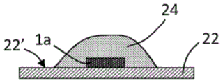
Fig. 3a shows a schematic view of an electrically operable device 1a of the type shown in fig. 1 and 2, which is positioned on a major surface 22' of a sheet of interlayer material 22, which in this example is a sheet of Ethylene Vinyl Acetate (EVA) having a thickness of about 0.2 mm. Fig. 3b shows a plan view of fig. 3a, i.e. a view in the direction of arrow 2a, which is perpendicular to main surface 22'. In fig. 3a, the electrically operable device 1a has not yet been fixed to the EVA sheet 22. However, the electrically operable device 1a may be secured to the EVA sheet 22 by use of a suitable adhesive.
Fig. 4 is used to illustrate another step in the production of an electrical device according to an aspect of the present invention. An assembly of EVA sheet 22 having electrically operable devices 1a thereon is provided and a layer of liquid adhesive 24 (EVA in this example) is deposited (i.e. by casting) on the electrically operable devices 1a so as to cover the electrically operable devices 1a and also to contact a portion of the major surface 22' of the EVA sheet 22. Other suitable materials for layer 24 include suitable resins or epoxy materials (which may be multi-component epoxy materials).
In this example, a layer 24 of liquid EVA, which is initially in solid form and then melted for subsequent deposition on the electrically operable device 1a as described above, may be applied using a hot glue gun or the like.
Due to the viscosity of the EVA, the layer 24 has a non-uniform thickness relative to the EVA sheet 22 (or major surface 22' of the EVA sheet 22), rather the layer has a convex surface and may be referred to in the art as a "blob", i.e. a blob of liquid EVA covering the electrically operable device 1 a. In the plan view shown in fig. 4b, the mass of liquid EVA is shown to have a circular periphery, but the shape of the periphery of the mass of liquid EVA may be non-circular.
Fig. 5 is used to illustrate subsequent steps in the production of an electrical device according to an aspect of the present invention. Before the layer 24 of liquid EVA cures, a leveling means is applied to flatten the layer 24 to provide a layer 24a of liquid EVA having a uniform (or substantially uniform) thickness relative to the EVA sheet 22. In this example, layer 24a has a thickness of 0.56mm, such that thickness 27 is about 0.76 mm.
The layer 24a of liquid EVA is hardened to form a solid layer of EVA. A layer 24a of solid EVA adheres and secures the electrically operable device 1a to the EVA sheet 22, i.e. encapsulates the electrically operable device on the EVA sheet 22.
In the form shown in figure 5a, once the layer 24a is a solid EVA layer, the assembly of EVA sheet 22 to which the electrically operable device 1a is secured by the layer 24a of solid EVA may be used as an electrical device 28 according to an aspect of the present invention. However, it is preferred to use additional processing steps to reduce the dimensions of electrical device 28 for subsequent use, as will be described in more detail below. In this way, the electrical device 28 is a parent electrical device from which child electrical devices can be produced.
Fig. 6 is used to illustrate another step in the production of an electrical device according to an aspect of the present invention.
Referring to fig. 5 and 6, starting with electrical device 28 (which is a parent electrical device), smaller electrical device 30 (a child electrical device) may be removed therefrom by cutting, stamping, or the like.
In this example, a knife is used to cut the electrical device 30 from the parent electrical device 28 to leave a hole (or aperture) 23 extending through the cured layer of EVA 24a and EVA sheet 22. Assuming that the electrically operable device 1a has been removed, the portion 29 consisting of the portion 22a of the EVA sheet 22 and the portion 24c of the cured layer of EVA 24a bonded thereto is no longer capable of functioning as an electrical device and is redundant and can be discarded.
The electrical device 30 which has been removed from the original electrical device 28 consists of a portion 24b of a cured layer of EVA 24a covering and engaging with the electrically operable device 1 a. Portion 24b is also joined to portion 22c of EVA sheet 22. The thickness of the electrical device 30 is shown by arrow 27 and is about 0.76mm in this example (the same as electrical device 28).
Although only one electrically operable device 1a is shown positioned on the EVA sheet 22 in fig. 3-6, there may be two or more such devices positioned on the EVA sheet 22. In such examples, the liquid layer 24 may extend over all electrically operable devices, or there may be one or more such liquid layers covering each electrically operable device, i.e. each electrically operable device may be covered by a respective liquid layer, and two or more of the respective liquid layers may be isolated from each other.
Figures 7-9 show examples in which a plurality of electrically operable devices 1b (of the type shown with reference to figures 1 and 2) are positioned on a suitable sheet of interlayer material such as EVA. In this example there are sixteen electrically operable devices 1 b.
Referring to fig. 7, fig. 7a shows a schematic plan view of an EVA sheet 32 located in the bottom of a suitable tray 33. Positioned on EVA sheet 32 are sixteen electrically operable devices, only 4 of which are labeled 1b and of the type described with reference to fig. 1 and 2. More or fewer electrically operable devices may be present on the EVA sheet 32. The electrically operable devices may be of the same type or of different types. In this example, the electrically-operable devices are positioned on the EVA sheet 32 in a grid-like manner, but the electrically-operable devices may be positioned on the EVA sheet 32 in any other configuration (which may be random).
Figure 7b shows a cross-sectional view of the assembly shown in figure 7a along line a-a'. The EVA sheet 32 has a thickness of about 0.2mm and rests flat on the bottom of the tray 33.
The tray 33 has a peripheral wall 33a, which peripheral wall 33a extends upwardly from the bottom of the tray by about 0.76 mm.
Figure 8 shows a schematic view of the assembly shown in figure 7b when a volume of liquid plastic has been deposited in the tray to cover the electrically operable device 1b and the exposed portions of the EVA sheet 32 (i.e. those portions of the EVA sheet 32 on which there is no electrically operable device). The volume of liquid plastic forms layer 34, and due to its viscosity, the thickness of layer 34 may not be uniform relative to EVA sheet 32. As shown in fig. 9, the liquid may be leveled to the level of the peripheral wall 33a of the tray 33 using a suitable leveling means. The liquid plastic may then be hardened to form a solid plastic layer 34' which encapsulates the electrically operable device 1 b. In this example, the combined thickness of the EVA sheet 32 and the solid layer 34' is about 0.76mm and is substantially set by the height of the peripheral wall 33a of the tray 33.
While fig. 9 may be used to illustrate the assembly of fig. 8 after the liquid forming layer 34 has been leveled, the same figure may be used to illustrate an assembly wherein the liquid forming layer 34' has a relatively low viscosity such that once the liquid has been deposited (i.e. by pouring) into the tray to cover electrically operable device 1b and EVA sheet 32, the liquid levels itself to the height of the peripheral wall 33a of tray 33.
Each electrically operable device 1b may then be removed from the assembly shown in figure 9 by suitable cutting, stamping or the like. It may not be possible to remove parts of the base of the tray 33 from the electrical apparatus produced in this way. Moreover, the solidified layer of the liquid in the area of the peripheral wall 33a of the tray will adhere thereto, making it difficult to separate therefrom.
Fig. 10 illustrates steps in an alternative method of performing an aspect of the present invention.
In fig. 10, the EVA sheet 32 has been placed on a suitable support (i.e. table) (not shown). The electrically operable device 1c (only two of which are marked) is then positioned at the desired location on the EVA sheet 32.
A suitable barrier 36 is then positioned on the EVA sheet 32 around the electrically operable devices positioned on the EVA sheet 32. The barrier 36 may be positioned on the EVA sheet 32 prior to positioning the electrically operable device thereon, in which case the electrically operable device is positioned on the EVA sheet 32 inside the barrier 36.
The barrier 36 may be formed of any suitable material, i.e., plastic, polyethylene, polycarbonate, and is suitably bonded to, preferably forms a seal with, the upper surface of the EVA sheet 32. The barrier 36 may be of unitary construction or formed from two or more segments suitably coupled together.
Figure 11 shows the assembly shown in figure 10 when a suitable liquid adhesive is poured into the area bounded by the barrier 36. The liquid adhesive forms a layer 34a covering the electrically operable device 1c and the EVA sheet 32. Depending on the viscosity of the liquid adhesive forming layer 34a, it may be desirable to level the liquid to form a layer 34a' of uniform thickness as shown in fig. 12. The layer 34a is then hardened to form a solid layer 34a ', which solid layer 34a' encapsulates the electrically operable device 1c positioned on the EVA sheet 32. Alternatively, the liquid may have a low viscosity, in which case no additional levelling step is required. If desired, layer 34a may not be leveled prior to being cured, wherein after being cured, layer 34a is provided with a uniform thickness by using suitable abrasive means or cutting.
Fig. 12 shows an assembly 38 of EVA sheet 32 having sixteen electrically operable devices 1c encapsulated by a solid layer 34a' and bounded by a barrier 36. The assembly 38 may be used as an electrical device according to an embodiment of the present invention. However, it is preferred that one or more of the electrically operable devices 1c are removed from the assembly 38 for subsequent use, as will be described below, i.e. the electrical device 38 is a parent electrical device for subsequently producing child electrical devices therefrom.
Fig. 13a shows a plan view of the assembly 38 shown in fig. 12. The assembly 38 serves as a parent electrical device that prepares sixteen child electrical devices, each similar to the electrical device 30 shown in fig. 6.
In a central region 38a of the assembly 38 there are sixteen enclosed electrically operable devices 1c (only one of which is labelled in figure 13 a) inside the barrier 36. The central region 38a is removed from the assembly 38 by cutting along a line 38b just inside the barrier 36 but spaced from the electrically operable device 1 c. Using a suitable cutting step (such as laser cutting, mechanical cutting or thermal cutting, etc.), the central region 38a of the assembly 38 may be removed to leave a portion 39 that does not contain electrically operable devices, as shown in fig. 13 b. The removed part 40 shown in fig. 13c contains sixteen encapsulated electrically operable devices 1c (only one of which is labelled in this figure).
In this example, the electrically operable devices are arranged in linear rows and columns as shown in fig. 13 c. There are four rows a, b, c and d and four columns i, ii, iii and iv. Each electrically operable device 1C may be removed from the portion 40 by cutting along the dashed line shown in fig. 13C, for example each row a may be removed from the portion 40 by cutting along the dashed line C-C'.
In this example, rows a and d have the same height, and rows b and c have the same height. Columns i, ii, iii and iv each have the same width, but may be different. The rows a, b, c, d may each have the same height.
Sixteen electrical devices of the type labeled 30 in fig. 6 are manufactured for subsequent use by cutting along the dashed lines shown in fig. 13 c. Each electrical device thus obtained is a child electrical device because it is produced from the assembly 38 (which is a parent electrical device).
Fig. 14 is used to illustrate how an electrical device 30 of the type shown in fig. 6 may be used to form an interlayer ply that includes the electrical device 30 and a sheet of interlayer material 50, according to an aspect of the present invention. Fig. 14a is a plan view and fig. 14b is a cross-sectional view along line D-D'. As is evident from the above, the electrical device 30 may be a sub-electrical device produced from an assembly of the type shown in fig. 13.
The sheet of interlayer material 50 having the holes 52 therein is placed on a suitable support (i.e. a table) (not shown). The electrical device 30 is then positioned in the aperture 52. The outer dimensions of the electrical device are slightly smaller than the major dimensions of the aperture 52 such that the electrical device is not secured within the aperture 52.
The electrical device 30 has been made such that its thickness (see label 27 on fig. 6) is the same or substantially the same as the thickness of the sheet of interlayer material 50, which may be between 0.38mm and 0.76 mm.
According to an aspect of the invention, the electrical device 30 is secured in the hole 52 in the sheet of interlayer material 50 using a suitable bonding means.
In the embodiment shown in fig. 15, a localized heat source is applied to the upper edge of the hole 52 and/or the electrical device 30, i.e. in the area indicated by the labels 53, 54. The localized heating locally softens and/or melts the interlayer material 50, thereby bonding the upper portion of the electrical device 30 to the wall 52a of the hole 52. The localized heating applied in the regions 53, 54 may also locally soften and/or melt the adhesive layer 24 b.
Similarly, localized heating may be applied to the lower edge of the aperture 52 and/or the electrical device 30, i.e., in the areas indicated by the labels 55, 56. Such localized heating may locally soften and/or melt interlayer material 50 and/or interlayer material 22c to engage the electrical device in aperture 52.
In an alternative embodiment as shown in fig. 16, the electronic device 30 is bonded in a hole 52 in the sheet of interlayer material 50 using an adhesive. When the electrical device 30 is located in the aperture 52 in the sheet of interlayer material 50, adhesive 57, 58 may be applied to the upper surface of the sheet of interlayer material 50 to also contact at least a portion of the electrical device 30 to engage the electrical device in the aperture 52. Similarly, adhesives 59, 60 may be applied to the lower surface of the sheet of interlayer material 50.
The adhesives 57, 58 may be applied as a bonding tape (i.e., an adhesive tape) that connects the sheet of interlayer material 50 to the electrical device 30. In such embodiments, the engagement strip need not extend over the entire major surface of the electrical device 30. However, in alternative embodiments, a sheet having contact adhesive on a major surface thereof may be used to connect the sheet of interlayer material 50 to the electrical device 30, in which case the sheet having contact adhesive thereon may cover the entire electrical device 30 on one side to secure the electrical device 30 in the aperture 52.
As shown in fig. 16, the adhesive 59, 60 may extend into any gap between the wall 52a of the aperture 52 and the outer wall of the electrical device 30 to provide engagement therebetween. The amount of adhesive 59, 60 that extends into any gap between the wall 52a of the aperture 52 and the outer wall of the electrical device 30 may depend on the viscosity of the adhesive 59, 60.
Fig. 17 shows another embodiment in which adhesive layers 61, 62 are used to join the electrical device 30 in the hole 52 in the sheet of interlayer material 50. The adhesive 61, 62 is applied to the outer wall of the electrical device 30 before the electrical device is positioned in the aperture 52. Thereafter, the adhesives 61, 62 contact the walls 52a of the holes 52 to bond the electrical device 30 thereto.
As shown in fig. 14-17, the purpose is to use a bonding means to secure the electrical device 30 in a hole 52 in the sheet of interlayer material 50 to make an interlayer sheet layer comprising the electrical device and the sheet of interlayer material. While it is preferred to secure the electrical device 30 in the aperture 52 in the sheet of interlayer material using an attachment means such as an adhesive, the adhesive may be a re-bondable adhesive such that the electrical device 30 is removably secured in the aperture 52.
An interlayer sheet having an electrical device 30 secured in a hole 52 in a sheet of interlayer material as described above may be used to construct a laminated glazing as shown in figures 18, 19 and 20. Each of fig. 18-20 is a schematic side view of a glazing.
In fig. 18a, an interlayer ply 70 of the type shown in fig. 15, 16 or 17 is shown between a first glass sheet 72 and a second glass sheet 74. Interlayer ply 70 couples first glass sheet 72 to second glass sheet 74. Conventional lamination conditions, such as elevated temperature and pressure, may be used to produce the laminated glazing 76. The interlayer ply 70 provides sufficient adhesive bonding with each of the first glass sheet 72 and the second glass sheet 74, in part because the major surface of the electrical device 30 is smaller than the major surface of the interlayer ply 70. Further, the material itself forming the main surface of the electric device 30 is an adhesive.
Suitable glasses for first glass sheet 72 and second glass sheet 74 include soda-lime-silica glass (commonly referred to as "soda-lime-silicate glass"). A typical soda-lime-silica glass composition is (by weight) SiO2 69-74%;Al2O3 0-3%;Na2O 10-16%;K2O 0-5%;MgO0-6%;CaO 5-14%;SO30-2% and Fe2O30.005-2 percent. The glass composition may also contain other additives, for example, refining aids and other colorants, which are typically present in amounts up to 2%. The transmitted glass color may be measured according to accepted standards, such as BS EN 410.
An exploded view of the laminated glazing 76 is shown in figure 18b for clarity.
In fig. 19a, an interlayer ply 70 of the type shown in fig. 15, 16 or 17 is shown between a first glass sheet 72 and a second glass sheet 74. In addition, there is another ply 80 of interlayer material, i.e., a ply (or sheet) of PVB, EVA, or the like. An interlayer ply 80 is positioned between the first glass sheet 72 and the interlayer ply 70. The interlayer ply 70 is located between the second glass sheet 74 and the interlayer ply 80.
The first glass sheet 72 is coupled to the second glass sheet 74 by an interlayer structure comprised of an interlayer ply 70 made in accordance with the present invention and a conventional ply of interlayer material 80. Conventional lamination conditions, such as elevated temperature and pressure, may be used to produce the laminated glazing 76'.
An exploded view of the laminated glazing 76' is shown in figure 19b for clarity.
In fig. 20a, an interlayer ply 70 of the type shown in fig. 15, 16 or 17 is shown between a first glass sheet 72 and a second glass sheet 74. Additionally, there is a first ply of interlayer material 80 and a second ply of interlayer material 80' between the first glass sheet 72 and the second glass sheet 74.
The first interlayer ply 80 is between the first glass sheet 72 and the interlayer ply 70. The interlayer plies 70 are located between the first and second conventional interlayer material plies 80, 80'. A second interlayer ply 80' is between interlayer ply 70 and second glass sheet 74.
The first glass sheet 72 is coupled to the second glass sheet 74 by an interlayer structure comprised of an interlayer ply 70 made according to the present invention, a first interlayer material ply 80, and a second interlayer material ply 80' arranged as described above. Conventional lamination conditions, such as elevated temperature and pressure, may be used to produce the laminated glazing 76'.
An exploded view of the laminated glazing 76' is shown in figure 20b for clarity.
In FIG. 19, the interlayer material plies 80 may be replaced by another ply 70 that has been made according to an aspect of the present invention.
In fig. 20, either or both of the interlayer material plies 80, 80' may be replaced by interlayer plies that have been made according to an aspect of the present invention.
Additional plies of interlayer material (conventional or made in accordance with the present invention) may be used in the construction of the laminated glazing, as desired.
Fig. 21-23 serve to illustrate how an additional flexible circuit 90 may be provided to assist in making electrical connections to electrically operable components mounted on a substrate (e.g. an electrically operable device of the type shown in fig. 1 and 2).
In fig. 21, a schematic isometric representation of an electrically operable device 1 as shown in fig. 1 and 2 and described in the related description thereof is shown. Fig. 22 is a schematic side view of fig. 21, i.e. a view looking in the direction of arrow 82.
Referring to fig. 21 and 22, located beneath the electrically operable apparatus 1 is an EVA sheet 22. The EVA sheet 22 has an upper major surface 22' and an opposite lower major surface (not labeled). The electrically operable device 1 is positioned on the EVA sheet 22 by moving the electrically operable device 1 in the direction of arrow 84 so that the electrically operable device 1 is in the position shown in dashed lines on the EVA sheet 22'. Reference is also made to fig. 3 b.
After positioning the electrically operable device 1 on the EVA sheet 22, the flexible circuit 90 is positioned on the electrically operable device 1 by moving the flexible circuit 90 in the direction of arrow 86.
The flexible circuit 90 includes a substrate 92 having a first major surface 92a and an opposing second major surface 92 b. When the flexible circuit 90 is positioned on the electrically operable device 1, the second main surface 92b of the substrate 92 faces the first main surface 5 of the substrate 3.
At one end of the substrate 92 on the second major surface 92b of the substrate 92 are first and second electrical connector regions 94, 96. At the opposite ends of the substrate 92 on the second major surface 92b of the substrate 92 are third and fourth electrical connector regions 98, 100.
The first electrical connector region 94 is in electrical communication with the third electrical connector region 98 via conductive tracks 102 on the second major surface 92b of the substrate 92 of the flexible circuit 90. The second electrical connector region 96 is in electrical communication with the third electrical connector region 100 via conductive tracks 104 on the second major surface 92b of the substrate 92 of the flexible circuit 90.
The conductive tracks 102, 104 may be screen printed conductive ink. Any or all of the first, second, third and fourth electrical connector regions 94, 96, 98, 100 may be screen printed conductive ink.
The substrate 92 of the flexible circuit 90 is similar to the substrate 3 of the electrically operable device 1. However, it is preferable that the substrate 92 be mechanically stronger than the substrate 3. For example, if the same material is used for the substrate 3 and the substrate 92, the substrate 92 is generally thicker than the substrate 3.
Alternatively, or in addition, the substrate 3 and the substrate 92 may be made of different materials, for example, different plastic materials. In some embodiments, a useful characteristic of the substrate 92 is the ability to bend without damaging the conductive tracks 102, 104 on the second major surface 92 b.
The flexible circuit 90 serves as an integral electrical connector to assist in providing electrical power to the electrically operable components 9 of the electrically operable device 1.
The first electrical connector region 94 on the substrate 92 of the flexible circuit 90 is arranged to align with the first electrical connector region 11 on the substrate 3 of the electrically operable device 1. The second electrical connector region 96 on the substrate 92 of the flexible circuit 90 is arranged to align with the second electrical connector region 13 on the substrate 3 of the electrically operable device 1 (indicated in fig. 21 by the dashed line extending therebetween). When the flexible circuit 90 is positioned on the electrically operable device 1, as previously described, the provision of electrical power to the third and fourth electrical connector regions 98, 100 on the substrate 92 of the flexible circuit 90 provides electrical power to the electrically operable components 9, since the first and second electrical connector regions 94, 96 on the substrate 92 are in electrical and mechanical communication with the respective first and second electrical connector regions 11, 13 on the substrate 3.
The third and fourth electrical connector regions 98, 100 are spaced apart from the first and second electrical connector regions 94, 96. The third and fourth electrical connector regions 98, 100 are also spaced from the periphery of the substrate 92 such that a portion of the substrate 92 may be removed by cutting along the ends of the substrate 92 and a line between the third and fourth electrical connector regions 98, 100 (as shown by line M-M'). The third and fourth electrical connector regions 98, 100 are also positioned on the substrate 3 in areas where there are no conductive areas or tracks on the first major surface of the substrate 3.
The connection between the first electrical connector region 94 on the substrate 3 of the flexible circuit and the first electrical connector region 11 on the substrate 5 of the electrically operable device 1 may be enhanced by using known electrical coupling methods such as local patches of conductive adhesive, anisotropic conductive adhesive such as CP923CM-25AC (http:// www.dexerials.jp/en/products /) manufactured by Dexerials or local application of an anisotropic conductive adhesive film.
In fig. 23 a schematic side view of a flexible circuit 90 on an electrically operable device 1 is shown, wherein the electrically operable device 1 is on an EVA sheet 22. In the figure, a space 105 between the flexible circuit 90 and the electrically operable device 1 is shown. With reference to the above, the space 105 is between the second main surface 92b of the substrate 92 of the flexible circuit 90 and the first main surface 5 of the substrate 3 of the electrically operable device 1. In an alternative embodiment, the second major surface 92b of the substrate 92 of the flexible circuit 90 or the first major surface 5 of the substrate 3 of the electrically operable device 1 may have a re-bondable adhesive thereon such that the substrate 92 is removably adhered to the substrate 3. In another alternative embodiment, there may be no space between the second main surface 92b of the substrate 92 of the flexible circuit 90 and the first main surface 5 of the substrate 3 of the electrically operable device 1.
Although in fig. 23 the flexible circuit 90 is aligned at one end with the periphery of the substrate 3, the flexible circuit may extend beyond the periphery of the substrate 3 of the electrically operable device 1.
Fig. 24 serves to illustrate how an electrical device according to an aspect of the present invention is produced. Fig. 24 is similar to fig. 12 previously described.
A plastic barrier 106 is positioned over the EVA sheet 22. An airtight seal is formed between the base of the barrier 106 and the first major surface 22' of the EVA sheet 22. In a similar manner to that shown in fig. 10, the barrier 106 completely surrounds the electrically operable device 1 having the flexible circuit 90 thereon when viewed in plan.
A suitable liquid plastic is poured into the area defined by the barrier 106 to completely cover the electrically operable device 1 with the flexible circuit 90 thereon. The liquid plastic layer 108 is leveled to the height of the barrier 106 by a leveling step or by allowing the liquid to settle.
The liquid plastic layer 108 is suitably hardened to form a solid plastic layer 108, the plastic layer 108 encapsulating the electrically operable device 1 with the flexible circuit 90 thereon, i.e. the electrically operable device 1 with the flexible circuit 90 thereon is encapsulated between the solid plastic layer 108 and the EVA sheet 22. A solid plastic layer 108 is also bonded to the first major surface 22' of the EVA sheet 22. It is clear that liquid plastic is an adhesive.
As discussed above, in fig. 23 and 24, a slight gap 105 is shown between the second major surface 92b of the substrate 92 and the first major surface 5 of the sheet of substrate 3 when the flexible circuit 90 is on the electrically operable device 1. The thickness of the gap 105 may be small enough that when liquid plastic is poured into the area bounded by the barrier 106, the liquid plastic cannot flow into the gap due to the viscosity of the liquid plastic. Alternatively, the flexible circuit 90 may be configured such that there is no gap between the second major surface 92b of the substrate 92 and the first major surface 5 of the substrate 3 when the flexible circuit board 90 is on the electrically operable device 1. Alternatively or additionally, one or more regions of the second major surface 92b may be provided with a suitable re-bondable adhesive such that the substrate 92 is removably attached to the substrate 3 and/or EVA sheet 22 when the flexible circuit 90 is located on the electrically-operable device 1. A suitable re-bondable adhesive helps to form a seal when liquid plastic is poured onto the electrically operable device 1.
The packaged electrically operable device 1 with the flexible circuit 90 thereon is used as a parent electrical device for producing a child electrical device. The electrically operable device 1 is secured to the EVA sheet 22 by a solid layer of plastic 108 and is removed therefrom by cutting along lines inside the barrier 106, i.e. along lines F-F 'and G-G' as shown in figure 24. The electrical device 110 thus manufactured is shown in figure 25a, where it can be seen that the substantially electrically operable device 1 is encapsulated between a portion 108 'of the cured plastics layer 108 and a portion 22' of the EVA sheet 22. If the sub-electrical device is produced by cutting along line H-H ' instead of cutting along line F-F ', a subsequent cutting step will be required to allow access to the flexible circuit 90, i.e. essentially by cutting along a portion of line F-F '.
In this example, the thickness 107 of the electrical device 110 is about 0.76 mm. A schematic isometric representation of the electrical device 110 is shown in fig. 25 b.
In accordance with an aspect of the present invention, electrical device 110 may be incorporated into a large sheet of suitable interlayer material 112 having a thickness of about 0.76mm in a manner similar to that described with respect to fig. 14-17. A schematic cross-sectional elevation view of the interlayer plies 114 so produced is shown in figure 26a and a schematic isometric representation of the interlayer plies 114 is shown in figure 26 b. In fig. 26b, the electrical device 110 is shown removed from the hole 116 in the large sheet of suitable interlayer material 112 for clarity.
The electrical device 110 may be engaged into the aperture by using suitable adhesive means as previously described, for example using a spot or strip of adhesive.
Although only one electrical device 110 is shown incorporated in a suitable sheet of interlayer material 112 in fig. 26a and 26b, there may be two or more such electrical devices incorporated in a suitable sheet of interlayer material 112.
The interlayer 114 may be used to construct a laminated glazing of the type shown in figures 18 to 20. A specific example is shown in fig. 27, which helps illustrate the benefits of the additional flex circuit 90.
As is apparent from fig. 26a and 26b, when the electrical device 110 is incorporated into a suitable sheet 112 of interlayer material, the electrical device 110 may be produced by cutting along the line H-H 'instead of the line F-F' shown in fig. 24, since the electrical device so produced is completely surrounded by the interlayer material 112 when in the hole 116.
Fig. 27 shows a schematic cross-sectional representation of a laminated glazing 120. The laminated glazing comprises a first sheet of soda-lime-silica glass 122 having a thickness of 2.1mm and a second sheet of soda-lime-silica glass 124 also having a thickness of 2.1 mm. The first sheet of soda lime silica glass 122 is coupled to the second sheet of soda lime silica glass by an interlayer ply 114 that includes the electrical device 110 secured in the aperture 116 of the appropriate sheet of interlayer material 112.
An expanded view of one end of a laminated glazing 120 is shown in figure 28. A portion 114' of the interlayer sheet 114 extends beyond the periphery of the first and second sheets 122, 124 of soda-lime-silica glass. The portion 114' includes an end portion of the substrate 92 of the flexible circuit 90 having the third and fourth electrical connector regions 98, 100 thereon such that the third and fourth electrical connector regions 98, 100 are not between the first and second sheets 122, 124 of soda lime silica glass. The first and second electrical connector regions 94, 96 are located between the first and second sheets 122, 124 of soda lime silica glass, as are the electrically operable component 9. A portion of the removed portion 114 'is cut along line J-J' to provide access to the flexible circuit 90.
Due to the weak bond between the substrate 3 and the substrate 92, for example due to the provision of a re-bondable adhesive (or possibly no bond therebetween) on the second main surface 92b of the substrate 92 and/or the first main surface 5 of the substrate 3 during production of an electrically operable device as described previously, the ends of the lower portion of the electrical device may be folded down (i.e. in the direction of arrow 117) to allow access to the third and fourth electrical connector regions 98, 100 on the portion 92' of the substrate 92 of the flexible circuit 90.
The addition of the flexible circuit 90 may allow a more reliable electrical connection to be made to power the electrically operable component 9, since the substrate 92 is mechanically more rigid and/or mechanically stronger and/or mechanically/chemically stronger than the substrate 3. For example, if no additional flexible circuit is used, but the first and/or second electrical connector regions 11, 13 extend beyond the periphery of the first and second pieces of soda-lime- silica glass 122, 124, it is possible to damage the first and/or second electrically conductive tracks 15, 17 on the substrate 3 unless the tracks are of suitable mechanical robustness. Furthermore, without providing the additional flexible circuit 90, a portion of the substrate 3 may be exposed, such that damage may be caused thereto, with the risk of breaking any conductive tracks thereon. The provision of the flexible circuit 90 may reduce the occurrence of such damage because the substrate 92 of the flexible circuit 90 is mechanically more rigid and/or mechanically stronger and/or mechanically/chemically stronger than the substrate 3.
The invention provides an electrical apparatus and a method for manufacturing the same. The electrical device may be incorporated into a sheet of interlayer material and the interlayer plies so produced may be used in the manufacture of laminated glazings. Such laminated glazings may be flat or curved and are particularly useful as windows for vehicles and/or buildings.
Claims (25)
1. A method of manufacturing an electrical device, comprising the steps of:
(i) providing an interlayer material layer having a first major surface and an opposing second major surface;
(ii) positioning at least a first electrically operable component on a first major surface of the first interlayer material layer, the first electrically operable component being mounted on a first circuit board; and
(iii) providing a layer of adhesive material to cover at least a portion of the first major surface of the layer of interlayer material and at least a portion of the first electrically operable component and/or at least a portion of the first circuit board;
such that after step (iii) the first electrically operable component is secured to the interlayer material layer by at least a portion of the adhesive material layer.
2. A method according to claim 1, wherein in step (ii) a first circuit board is positioned on the first major surface of the interlayer material layer such that the first circuit board is located between the interlayer material layer and the first electrically operable component.
3. A method according to claim 1 or claim 2, wherein in step (iii), the adhesive material is provided as a liquid, preferably by casting or spraying, to provide the layer of adhesive material.
4. A method according to claim 3, wherein after step (iii) the liquid is subjected to a curing step, preferably wherein the curing step of the liquid comprises a solidifying step and/or a hardening step, preferably wherein the curing step of the liquid comprises a thermal heating step and/or an irradiation step, preferably an ultraviolet irradiation step.
5. The method according to claim 3 or 4, wherein the liquid is leveled to achieve a uniform thickness with respect to the first layer of interlayer material, more preferably with respect to the first main surface and/or the second main surface of the first layer of interlayer material.
6. The method according to claim 4 or claim 5, wherein the surface of the cured layer of adhesive material not facing the first interlayer material layer is textured and/or provided with a coating.
7. The method according to any one of claims 3 to 6, wherein the liquid comprises a two-component system comprising at least a first component and a second component, preferably wherein the first component is mixed with the second component during step (iii) before or after being provided.
8. A method according to any preceding claim, wherein the layer of adhesive material is between 0.3mm and 3.0mm thick, and/or wherein the layer of interlayer material is between 0.3mm and 2.0mm thick, and/or wherein the layer of adhesive material covers the entire electrically operable component and/or the entire first circuit board.
9. The method of any preceding claim, wherein after step (i) a first barrier is provided on the first major surface of the ply of interlayer material or around the periphery of the ply of interlayer material, and after step (ii) at least a portion of the first circuit board is inside the first barrier, preferably wherein the first barrier surrounds the first circuit board such that the entire first circuit board is inside the first barrier.
10. A method according to any preceding claim, wherein after step (ii) at least a second electrically operable component is positioned on the interlayer material layer, the second electrically operable component being mounted on a second circuit board, further wherein the second electrically operable component is spaced from the first electrically operable device and/or the first circuit board is spaced from the second circuit board.
11. A method according to claim 10, wherein during step (iii) the layer of adhesive material also covers at least a part of the second electrically operable component and/or at least a part of the second circuit board, preferably wherein the layer of adhesive material also covers the entire second electrically operable component and/or the entire second circuit board, or a method according to claim 10, wherein after step (iii) a layer of second adhesive material is provided to cover at least a part of the second electrically operable component and/or at least a part of the second circuit board, preferably wherein the layer of second adhesive material is provided as a liquid.
12. A method according to any preceding claim, wherein after step (iii), at least a portion of the first circuit board on which the first electrically operable component is mounted is removed from the interlayer material layer, preferably by a cutting step or a stamping step, to produce an electrical device which is a sub-electrical device.
13. A method according to any preceding claim, wherein prior to step (iii), a flexible circuit is positioned on the ply of interlayer material or first circuit board, the flexible circuit comprising a substrate having a first major surface and an opposing second major surface, the first or second major surface of the substrate of the flexible circuit comprising a first electrical connector region thereon in electrical communication with a second electrical connector region on the first or second major surface of the substrate of the flexible circuit by electrically conductive tracks; wherein the flexible circuit is positioned such that the second electrical connector region on the substrate of the flexible circuit is in electrical, and preferably mechanical, communication with the first electrical connector region on the first circuit board.
14. The method of claim 13, wherein the substrate of the flexible circuit includes, on the first or second major surface thereof, a third electrical connector region in electrical communication with a fourth electrical connector region on the first or second major surface of the substrate of the flexible circuit via electrically conductive tracks; wherein the flexible circuit is positioned such that the fourth electrical connector region on the substrate of the flexible circuit is in electrical, and preferably mechanical, communication with the second electrical connector region on the first circuit board.
15. A method according to any preceding claim, wherein after step (iii), the method comprises incorporating the electrical device into a hole in a further sheet of interlayer material, wherein incorporating the electrical device into a hole in the further sheet of interlayer material comprises the steps of: providing a sheet of interlayer material having a first major surface and an opposing second major surface; removing at least a first portion of the sheet of interlayer material to create an aperture in the sheet of interlayer material, the aperture in the sheet of interlayer material having at least a first wall between a first major surface and a second major surface of the sheet of interlayer material; positioning at least a portion of the electrical device in an aperture; an electrical device is secured to at least a portion of the first major surface and/or the second major surface of the sheet of interlayer material and/or at least a portion of the first wall of the aperture in the sheet of interlayer material using an attachment means.
16. The method of claim 15, wherein the entire electrical device is within the aperture, and/or wherein the joining means comprises a fusion step and/or an adhesive.
17. A method according to any preceding claim, wherein in step (i) the ply of interlayer material is provided as a sheet of interlayer material.
18. The method according to any one of the preceding claims, wherein the interlayer material comprises polyvinyl butyral (PVB), a copolymer of ethylene, such as Ethylene Vinyl Acetate (EVA) or polyurethane, in particular Thermoplastic Polyurethane (TPU); and/or wherein the binder material comprises polyvinyl butyral (PVB), copolymers of ethylene, such as Ethylene Vinyl Acetate (EVA) or polyurethane, in particular Thermoplastic Polyurethane (TPU).
19. An electrical device, comprising:
at least one electrically operable component mounted on a first circuit board, the first circuit board having a first major surface and an opposing second major surface;
at least one ply of interlayer material having an outer major surface; and
at least one layer of adhesive material having an outer major surface;
wherein the first circuit board on which the at least one electrically operable component is mounted is between the outer major surface of the at least one ply of interlayer material and the outer major surface of the at least one ply of adhesive material;
further wherein the first circuit board is secured to the interlayer material layer at least by an adhesive material layer;
it is characterized in that the preparation method is characterized in that,
the electrical device has a first outer surface and an opposite second outer surface, wherein
(a) The first outer surface of the electrical device comprises an outer major surface of the at least one ply of interlayer material, and the second outer surface of the electrical device comprises an outer major surface of the at least one ply of adhesive material,
or
(b) The first outer surface of the electrical device comprises an outer major surface of the at least one layer of adhesive material, and the second outer surface of the electrical device comprises an outer major surface of the at least one layer of interlayer material.
20. The electrical device of claim 19 wherein the electrically operable component has first and second input terminals for providing electrical power thereto, and wherein the first circuit board includes a first electrical connector region in electrical communication with the first input terminal of the electrically operable device, further wherein the electrical device includes a flexible circuit including a substrate having a first major surface and an opposing second major surface, the first or second major surface of the substrate of the flexible circuit including the first electrical connector region thereon in electrical communication with the second electrical connector region on the first or second major surface of the substrate of the flexible circuit by conductive tracks, the first electrical connector region on the substrate of the flexible circuit in electrical and mechanical communication with the first electrical connector region on the first circuit board, such that electrical power is provided to the at least one electrically operable component when the second input terminal of the at least one electrically operable component is brought into electrical communication with the first output terminal of the suitable power source and the second electrical connector region of the flexible circuit is brought into electrical communication with the second output terminal of the suitable power source, preferably wherein the first electrical connector region of the flexible circuit and the second electrical connector region of the flexible circuit are on the second major surface of the substrate of the flexible circuit and preferably the first electrical connector region of the flexible circuit is in electrical communication with the second electrical connector region of the flexible circuit by conductive tracks on the second major surface of the substrate of the flexible circuit.
21. The electrical device of claim 20, wherein the substrate of the flexible circuit includes a third electrical connector region on the first or second major surface of the substrate of the flexible circuit in electrical communication with a fourth electrical connector region on the first or second major surface of the substrate of the flexible circuit by conductive tracks, the third electrical connector region on the substrate of the flexible circuit in electrical and mechanical communication with the second electrical connector region on the first circuit board in electrical communication with the second input terminal of the at least one electrically-operable component, wherein upon placing the fourth electrical connector region of the flexible circuit in electrical communication with the first output terminal of the suitable power source and placing the second electrical connector region of the flexible circuit in electrical communication with the second output terminal of the suitable power source, providing electrical power to the at least one electrically operable component, preferably wherein the third electrical connector region of the flexible circuit and the fourth electrical connector region of the flexible circuit are on the second major surface of the substrate of the flexible circuit, and preferably the third electrical connector region of the flexible circuit is in electrical communication with the fourth electrical connector region of the flexible circuit via electrically conductive tracks on the second major surface of the substrate of the flexible circuit.
22. The electrical device of claim 20 or claim 21, wherein the second major surface of the substrate of the flexible circuit faces the first major surface of the first circuit board, preferably wherein the second major surface of the substrate of the flexible circuit is in direct contact with at least a portion of the first major surface of the first circuit board and/or wherein temporary adhesive means is located between at least a portion of the first major surface of the first circuit board and the second major surface of the substrate of the flexible circuit, preferably wherein the temporary adhesive means is a re-bondable adhesive.
23. The electrical device of any one of claims 19 to 22, wherein the electrical device is part of an interlayer ply adapted to couple two sheets of glass together, wherein the interlayer ply comprises a sheet of interlayer material having a first major surface and an opposing second major surface, there being an aperture in the sheet of interlayer material having walls extending between the first and second major surfaces of the sheet of interlayer material, the electrical device being positioned in the aperture in the sheet of interlayer material and bonded to at least a portion of the wall of the aperture and/or at least a portion of the first and/or second major surfaces of the sheet of interlayer material, preferably wherein the sheet of interlayer material comprises polyvinyl butyral (PVB), a copolymer of ethylene, such as Ethylene Vinyl Acetate (EVA) or polyurethane, in particular Thermoplastic Polyurethanes (TPU).
24. The electrical device according to any one of claims 19 to 23, wherein at least one of the at least one layer of interlayer material and the at least one layer of adhesive material comprises polyvinyl butyral (PVB), a copolymer of ethylene, such as Ethylene Vinyl Acetate (EVA) or polyurethane, in particular Thermoplastic Polyurethane (TPU).
25. A laminated glazing comprising at least one sheet of glazing material, preferably glass, and an electrical device according to any of claims 19 to 24, wherein the electrical device is coupled to the at least one sheet of glazing material by the at least one sheet of interlayer material or the at least one layer of adhesive material.
Applications Claiming Priority (3)
| Application Number | Priority Date | Filing Date | Title |
|---|---|---|---|
| GBGB1814347.9A GB201814347D0 (en) | 2018-09-04 | 2018-09-04 | Electrical device, interlayer ply including an electrical device and methods for making said electrical device and interlayer ply |
| GB1814347.9 | 2018-09-04 | ||
| PCT/GB2019/052455 WO2020049292A1 (en) | 2018-09-04 | 2019-09-04 | Electrical device, interlayer ply including an electrical device and methods for making said electrical device and interlayer ply |
Publications (1)
| Publication Number | Publication Date |
|---|---|
| CN112772004A true CN112772004A (en) | 2021-05-07 |
Family
ID=63921022
Family Applications (1)
| Application Number | Title | Priority Date | Filing Date |
|---|---|---|---|
| CN201980064632.5A Pending CN112772004A (en) | 2018-09-04 | 2019-09-04 | Electrical device, interlayer sheet comprising electrical device and method for manufacturing electrical device and interlayer sheet |
Country Status (6)
| Country | Link |
|---|---|
| US (1) | US11812557B2 (en) |
| EP (1) | EP3847873B1 (en) |
| JP (1) | JP2021536677A (en) |
| CN (1) | CN112772004A (en) |
| GB (1) | GB201814347D0 (en) |
| WO (1) | WO2020049292A1 (en) |
Family Cites Families (11)
| Publication number | Priority date | Publication date | Assignee | Title |
|---|---|---|---|---|
| EP0603739B1 (en) | 1992-12-23 | 1995-10-25 | Rheinmetall Industrie Aktiengesellschaft | Stress resistant electronic assembly |
| JP3320610B2 (en) | 1996-04-25 | 2002-09-03 | 富士通テン株式会社 | Electronic device sealing structure |
| JPH10284630A (en) | 1997-04-01 | 1998-10-23 | Fujitsu Ten Ltd | Sealing structure of electronic component |
| GB0216787D0 (en) | 2002-07-19 | 2002-08-28 | Pilkington Plc | Laminated glazing panel |
| US9338915B1 (en) * | 2013-12-09 | 2016-05-10 | Flextronics Ap, Llc | Method of attaching electronic module on fabrics by stitching plated through holes |
| BE1021978B1 (en) | 2013-12-13 | 2016-02-01 | Agc Glass Europe | AUTOMOBILE GLAZING |
| DE102016205966A1 (en) * | 2016-04-11 | 2017-10-12 | Zf Friedrichshafen Ag | Electronic unit with ESD protection arrangement |
| FR3051727B1 (en) | 2016-05-26 | 2018-05-18 | Saint-Gobain Glass France | GLAZING OF LUMINOUS SIGNALING, VEHICLE INCORPORATING AND MANUFACTURING. |
| EP3494645A1 (en) | 2016-08-05 | 2019-06-12 | Pilkington Group Limited | Laminated glazing |
| FR3061404B1 (en) * | 2016-12-27 | 2022-09-23 | Packaging Sip | METHOD FOR THE COLLECTIVE MANUFACTURING OF HERMETIC ELECTRONIC MODULES |
| DE102017204338A1 (en) * | 2017-03-15 | 2018-09-20 | Robert Bosch Gmbh | Electronic control module and method of manufacturing an electronic control module |
-
2018
- 2018-09-04 GB GBGB1814347.9A patent/GB201814347D0/en not_active Ceased
-
2019
- 2019-09-04 CN CN201980064632.5A patent/CN112772004A/en active Pending
- 2019-09-04 EP EP19766310.7A patent/EP3847873B1/en active Active
- 2019-09-04 WO PCT/GB2019/052455 patent/WO2020049292A1/en unknown
- 2019-09-04 US US17/273,249 patent/US11812557B2/en active Active
- 2019-09-04 JP JP2021512387A patent/JP2021536677A/en active Pending
Also Published As
| Publication number | Publication date |
|---|---|
| EP3847873B1 (en) | 2024-01-24 |
| WO2020049292A1 (en) | 2020-03-12 |
| US20210329787A1 (en) | 2021-10-21 |
| GB201814347D0 (en) | 2018-10-17 |
| JP2021536677A (en) | 2021-12-27 |
| US11812557B2 (en) | 2023-11-07 |
| EP3847873A1 (en) | 2021-07-14 |
Similar Documents
| Publication | Publication Date | Title |
|---|---|---|
| US5026452A (en) | Method of producing IC cards | |
| JP6795698B2 (en) | A method for manufacturing a composite pane with functional elements | |
| CN110914055B (en) | Multilayer film with electrically switchable optical properties and improved electrical contact | |
| CN108990319B (en) | Stepped plate pressing and stacking structure and manufacturing method thereof | |
| JP2001319775A (en) | Sealing method of organic el display device and sealing structure | |
| JPH09116322A (en) | Glass antenna and connector | |
| US7520416B2 (en) | Transparent window with non-transparent contact surface for a soldering bonding | |
| US20220176680A1 (en) | Glass resin laminate | |
| CN111128039A (en) | Flexible LED thin film display screen and preparation method thereof | |
| JP6845321B2 (en) | Composite panes and methods for manufacturing composite panes | |
| CN113207287A (en) | Composite glass pane with a functional element embedded in a thermoplastic intermediate layer and a venting structure | |
| CN112599570A (en) | Display panel and preparation method thereof | |
| EP3847873B1 (en) | Electrical device, interlayer ply including an electrical device and methods for making said electrical device and interlayer ply | |
| CN111936445B (en) | Glass structure, adhesive structure, and method for producing glass structure | |
| JPWO2019150037A5 (en) | ||
| WO2021070769A1 (en) | Bonded body manufacturing method and bonded body manufacturing device | |
| CN210805047U (en) | Flexible LED film display screen | |
| CN110602882B (en) | Blind slot printed circuit board and processing method thereof | |
| CN113960842A (en) | Dimming glass and preparation method thereof | |
| US6617983B1 (en) | Glass keyboard, and method for producing a glass keyboard | |
| US20230032295A1 (en) | Window glass for vehicle | |
| EP0435144A1 (en) | Notch sealant for heatable windshield | |
| WO2024060252A1 (en) | Dimming structure, as well as preparation method therefor, and dimming device | |
| CN216118321U (en) | Electrochromic device and dimming glass | |
| CN218906535U (en) | Light-adjusting laminated glass |
Legal Events
| Date | Code | Title | Description |
|---|---|---|---|
| PB01 | Publication | ||
| PB01 | Publication | ||
| SE01 | Entry into force of request for substantive examination | ||
| SE01 | Entry into force of request for substantive examination |