Disclosure of Invention
The invention mainly aims to provide a flexible electronic substrate, a preparation method and a preparation system thereof, and aims to solve the problems that the background level is high, large-scale preparation cannot be realized and the like in the prior art.
According to a first aspect of the present invention, there is provided a method of manufacturing a flexible electronic substrate, characterized by comprising the steps of: pretreating the substrate; performing ion implantation on the pretreated substrate surface to obtain a first metal; depositing a first metal on the surface of the substrate implanted with the first metal ions; and depositing a second metal on the surface of the substrate on which the first metal is deposited.
Preferably, the substrate is a polytetrafluoroethylene film.
Preferably, the first metal is a group iv metal.
Preferably, the second metal is copper.
Preferably, the ion implantation is by a metal vapor vacuum arc ion source.
Preferably, the deposition is by a magnetic filtered cathode vacuum arc source.
Preferably, the preparation method further comprises the steps of: and electrochemically depositing the second metal on the surface of the substrate on which the second metal is deposited.
Preferably, after one surface of the substrate is subjected to ion implantation of the first metal, deposition of the first metal and deposition of the second metal, the other surface is subjected to ion implantation of the first metal, deposition of the first metal and deposition of the second metal.
According to a second aspect of the present invention, there is provided a system for producing a flexible electronic substrate, comprising: the pretreatment device is used for pretreating the substrate; the ion implantation device is used for performing ion implantation on the pretreated substrate surface to obtain a first metal; the first deposition device is used for depositing first metal on the surface of the substrate implanted with the first metal ions; and the second deposition device is used for depositing a second metal on the surface of the substrate on which the first metal is deposited.
Preferably, the substrate is a polytetrafluoroethylene film.
Preferably, the first metal is a group iv metal.
Preferably, the second metal is copper.
Preferably, the ion implantation apparatus is a metal vapor vacuum arc ion source.
Preferably, the first deposition device and/or the second deposition device is a magnetic filtered cathode vacuum arc source.
Preferably, the preparation system further comprises an electrochemical device for electrochemically depositing the second metal on the surface of the substrate on which the second metal is deposited.
Preferably, the preparation system further comprises a reversing turnover device for turning over the substrate, one surface of which is treated by the ion implantation device, the first deposition device and the second deposition device in sequence, so as to convey the substrate to the ion implantation device, the first deposition device and the second deposition device again to treat the other surface of the substrate in sequence.
According to a third aspect of the present invention, there is provided a flexible electronic substrate characterized by being produced by the foregoing production method for a flexible electronic substrate or the foregoing production system for a flexible electronic substrate.
Compared with the prior art, according to the technical scheme, the flexible electronic substrate for circuit transmission of weak signals of the detector is prepared, and has the advantages of low background, low temperature resistance, long size and low cost. By combining a Metal Vapor Vacuum Arc (MEVVA) technology and a Magnetic Filter Cathode Vacuum Arc (FCVA) technology, a low-background Polytetrafluoroethylene (PTFE) film is used as a substrate, and Ni ion implantation is utilized to realize surface modification. The Ni/Cr and Cu transition layer grows on the modified substrate through magnetic filtration, and finally the PTFE-Cu flexible electronic substrate is prepared through electrochemical deposition, and the prepared substrate meets the requirement that the thickness is more than 0.8N/mm after being soaked in liquid nitrogen, and has excellent binding force. The method can be used for preparing two layers of copper-clad flexible plates, has low cost without adhesion, can quickly realize the preparation of roll-to-roll and long base materials, and has wide application prospect.
Detailed Description
In order to make the objects, technical solutions and advantages of the present invention more apparent, the present invention will be described in further detail below with reference to the accompanying drawings and specific embodiments.
In the following description, references to "one embodiment," "an embodiment," "one example," "an example," etc., indicate that the embodiment or example so described may include a particular feature, structure, characteristic, property, element, or limitation, but every embodiment or example does not necessarily include the particular feature, structure, characteristic, property, element, or limitation. Moreover, repeated use of the phrase "in one embodiment" does not necessarily refer to the same embodiment, although it may.
Certain features that are well known to those skilled in the art have been omitted from the following description for the sake of simplicity.
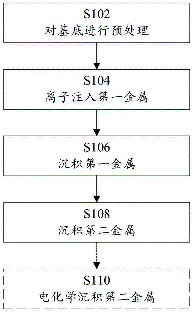
FIG. 1 schematically illustrates a method of making a flexible electronic substrate according to one embodiment of the present invention. The preparation method comprises the following steps:
step S102, preprocessing the substrate. Preferably, the substrate is a polytetrafluoroethylene film.
Step S104, ion implantation of a first metal is performed on the pretreated substrate surface. Preferably, the first metal is a group iv metal. Preferably, the ion implantation is by a metal vapor vacuum arc ion source.
Step S106, depositing a first metal on the surface of the substrate implanted with the first metal ions. Preferably, the deposition is by a magnetic filtered cathode vacuum arc source.
And S108, depositing a second metal on the surface of the substrate on which the first metal is deposited. Preferably, the second metal is copper.
The preparation method may further include step S110 of electrochemically depositing a second metal on the surface of the substrate on which the second metal is deposited.
The first metal may be ion-implanted, deposited, and the second metal may be deposited on one surface of the substrate, and then the first metal may be ion-implanted, deposited, and the second metal may be deposited on the other surface.
FIG. 2 illustrates a system for preparing a flexible electronic substrate according to one embodiment of the present invention. The preparation system comprises: a pretreatment apparatus 202, an ion implantation apparatus 204, a first deposition apparatus 206, and a second deposition apparatus 208.
The pre-treatment device 202 is used to pre-treat the substrate. Preferably, the substrate is a polytetrafluoroethylene film.
The ion implantation device 204 is used for ion implanting the first metal into the pretreated substrate surface. Preferably, the first metal is a group iv metal. Preferably, the ion implantation apparatus is a metal vapor vacuum arc ion source.
The first deposition device 206 is used to deposit a first metal on the substrate surface where the first metal ions are implanted. Preferably, the first deposition device is a magnetic filtered cathode vacuum arc source.
The second deposition device 208 is used to deposit a second metal on the substrate surface where the first metal is deposited. Preferably, the second metal is copper. Preferably, the second deposition means is a magnetic filtered cathode vacuum arc source.
The fabrication system may further include an electrochemical device 210 for electrochemically depositing a second metal on the substrate surface on which the second metal is deposited.
The preparation system can also comprise a reversing turnover device 212 for turning over the substrate, which is treated on one surface by the ion implantation device 204, the first deposition device 206 and the second deposition device 208 in sequence, so as to convey the substrate to the ion implantation device 204, the first deposition device 206 and the second deposition device 208 for treatment on the other surface in sequence.
The following details the preparation of very low temperature, low background flexible electronic substrates according to the present invention.
Example 1
Using a device integrating the MEVVA and the FCVA; and (3) taking the low-background PTFE film as a substrate, and carrying out surface modification on the low-background PTFE film by adopting an MEVVA source to implant metal elements of the IV main group. Performing magnetic filtration on a substrate to grow a metal element of a fourth main group and a Cu transition layer, and finally preparing a PTFE-Cu flexible electronic substrate through electrochemical deposition; the prepared substrate and the substrate after being soaked in liquid nitrogen both meet the requirement of more than 0.8N/mm.
Therefore, the invention utilizes MEVVA and FCVA methods to carry out surface modification on PTFE and deposit a metal element of the IV main group and a Cu transition layer so as to enhance the bonding force of PTFE and subsequent electrochemical copper plating. And further obtaining a copper film with a uniform structure through electrochemical deposition, and realizing the preparation of the PTFE double-sided copper-clad substrate.
Example 2
(1) Pretreatment: and drying the PTFE in an oven at 60-80 ℃. The thickness of the PTFE is 0.1-0.5 mm.
(2) The pretreated PTFE was fixed on a sample stage, and the chamber was evacuated to 5X 10⁻³~1×10⁻⁴Vacuum of Pa。
(3) And (3) cleaning the surface of the PTFE by using an argon (Ar) ion source, wherein the power is 600-900W, and the cleaning time is 50-150 s.
(4) Carrying out 5-10 keV IV main group metal element ion implantation by adopting an MEVVA source, rotating a sample stage at the frequency of 10-30 Hz for 60-150 s, and carrying out the implantation at the dosage of 1016~1019ions/cm2。
(5) And carrying out magnetic filtration and deposition on the sample after ion implantation, wherein the FCVA left arc source and right arc source respectively use the metal element of the IV main group and Cu as targets, the deposition current and time of the metal element of the IV main group are 80-120A and 3-8 min, the deposition current and time of Cu are 80-120A and 5-30 min, and the metal element of the IV main group and Cu thin film with the thickness of about 10-40 nm and 20-80 nm grow on the substrate.
(6) The modified PTFE is added in 0.05-0.1M CuSO4Carrying out electrochemical copper plating on the solution for 15-50 min, wherein the thickness of a deposited film is 2-12 mu m; the peel strength of the further test sample was 0.8N/mm.
(7) And (3) immersing the prepared PTFE-Cu flexible substrate into liquid nitrogen for 30-60 days, and taking out, wherein the peel strength still meets the requirement of more than 0.8N/mm.
The effect on the bonding strength of the final PTFE surface was verified by adjusting the MEVVA ion source and the FCVA1, FCVA2 parameter settings below.
Example 2a
(1) Pretreatment: drying the PTFE in an oven at 80 ℃.
(2) The pretreated PTFE was fixed on a sample stage, and the chamber was evacuated to 5X 10⁻³Pa of high vacuum.
(3) The surface of PTFE was cleaned with an Ar ion source at a power of 800W for 100 s.
(4) Injecting 7keV IV main group metal element ions by using MEVVA source, rotating the sample stage at 20Hz for 100s, and injecting 10 doses17ions/cm2。
(5) And carrying out magnetic filtration deposition on the sample after ion implantation, wherein the FCVA left arc source and right arc source respectively use the IV main group metal element and Cu as target materials, the IV main group metal element deposition current and time are 100A and 5min, the Cu deposition current and time are 100A and 20min, and the IV main group metal element and Cu thin film with the thickness of about 10nm and 20nm grow on the substrate.
(6) Adding the modified PTFE into 0.05M CuSO4Performing electrochemical copper plating on the solution, and plating a film for 45min under the current of 0.4A, wherein the thickness of the deposited film is 5.4 mu m; the peel strength of the further test sample was 1.03N/mm.
(7) And (3) immersing the prepared PTFE-Cu flexible substrate into liquid nitrogen for 30-60 days, and taking out, wherein the peel strength still meets 0.8N/mm.
Example 2b
(1) Pretreatment: drying the PTFE in an oven at 70 ℃.
(2) The pretreated PTFE was fixed on a sample stage, and the chamber was evacuated to 5X 10⁻³Pa of high vacuum.
(3) The surface of PTFE was cleaned with an Ar ion source at a power of 800W for 100 s.
(4) Performing ion implantation of IV main group metal element with 8keV by using MEVVA source, rotating the sample stage at 20Hz for 200s, and performing implantation at a dose of 1018ions/cm2。
(5) And carrying out magnetic filtration deposition on the sample after ion implantation, wherein the FCVA left arc source and right arc source respectively use the IV main group metal element and Cu as targets, the IV main group metal element Cr deposition current and time are 90A and 8min, the Cu deposition current and time are 90A and 25min, and IV main group metal element and Cu thin film with the thickness of about 15nm and 35nm are grown on the substrate.
(6) Adding the modified PTFE into 0.05M CuSO4Performing electrochemical copper plating on the solution, and plating a film for 30min at the current of 0.4A to obtain a deposited film with the thickness of 4.3 mu m; the peel strength of the further test sample was 0.83N/mm.
(7) And (3) immersing the prepared PTFE-Cu flexible substrate into liquid nitrogen for 30-60 days, and taking out, wherein the peel strength still meets 0.8N/mm.
Example 2c
(1) Pretreatment: drying the PTFE in an oven at 60 ℃.
(2) The pretreated PTFE was fixed on a sample stage, and the chamber was evacuated to 1X 10⁻⁴High vacuum of Pa。
(3) The surface of PTFE was cleaned with an Ar ion source at a power of 900W for a cleaning time of 80 s.
(4) Implanting metal ions of IV main group at 8keV with MEVVA source, rotating the sample stage at 20Hz for 150s, and injecting at 5 × 10 dose17ions/cm2。
(5) And carrying out magnetic filtration deposition on the sample after ion implantation, wherein the FCVA left arc source and right arc source respectively use the IV main group metal element and Cu as targets, the IV main group metal element deposition current and time are 110A and 6min, the Cu deposition current and time are 110A and 25min, and the IV main group metal element and Cu thin film with the thickness of about 15nm and 30nm grow on the substrate.
(6) Adding the modified PTFE into 0.05M CuSO4Performing electrochemical copper plating on the solution, and plating a film for 15min at the current of 0.7A to form a deposited film with the thickness of 3 mu m; the peel strength of the further test sample was 0.9N/mm.
(7) The prepared PTFE-Cu flexible substrate is taken out after being immersed in liquid nitrogen for 45 days, and the peel strength still meets 0.8N/mm.
Fig. 3a and 3c show PTFE raw materials of 0.5mm and 0.05mm thickness, and fig. 3b and 3d show corresponding PTFE-Cu flexible copper clad substrates.
Fig. 4a and 4b show the PTFE composite membrane after the modified and transition layer deposition.
Fig. 5a, 5b, 5c show the micro-topography SEM images of the flexible copper clad substrate, corresponding to examples 2a, 2b, 2c, respectively.
Fig. 6a, 6b, 6c show AFM micro-topography images of 2 different regions after 30 days of liquid nitrogen temperature soak.
Example 3
In order to implement the above method for manufacturing a flexible electronic substrate, based on the above embodiments, this embodiment proposes an apparatus for realizing large-scale manufacturing in a roll-to-roll manner, as shown in fig. 7, which includes the following apparatuses: a feeding and discharging device, an injection device, a deposition device, a vacuum device and a roll-to-roll matching roller device.
The vacuum device, namely the vacuum pump, is provided with a mechanical pump and a molecular pump, wherein the mechanical pump mainly pumps low vacuum, the molecular pump pumps high vacuum, and the mechanical pump and the molecular pump are required to be connected in series and matched to achieve higher vacuum.
And the injection device is used for injecting the IV main group metal element into the PTFE by utilizing an MEVVA ion source and cleaning the substrate layer. It should be noted that the MEVVA ion source mainly comprises a plasma generation region, i.e. a metal vapor vacuum arc discharge region, and an ion beam extraction region. MEVVA ion implantation adopts energy-carrying ion beams generated by an MEVVA ion source to bombard the surface of PTFE for ion implantation, so that the physical and chemical properties of the surface of the material are changed, and the film and the PTFE can be firmly combined.
The deposition device utilizes FCVA1 to obtain a film layer related to the metal element of the IV main group on the surface after ion implantation, and then Cu element is implanted through FCVA2, and the two are combined to realize an interface with better bonding energy.
The PTFE surface modification step is carried out on a single surface, and after the single-surface preparation is completed, the untreated surface is further subjected to the device treatment of MEVVA ion source, FCVA1 and FCVA2 by changing the counter rotation of a cooling roller.
The front side and the back side of the flexible electronic substrate are both required to be treated, after the first round of feeding is completed and the materials pass through MEVVA, FCVA1 and FCVA2, the materials rolled by the rollers reversely return to the cooling roller corresponding to the MEVVA, and the back side of the materials is treated by the MEVVA, FCVA1 and FCVA2, so that the front side and the back side of the flexible electronic substrate can be well combined with Cu.
The invention has the beneficial effects that the surface modification of PTFE is realized by the MEVVA method, the bonding force between PTFE and copper is enhanced by the IV main group metal element and the Cu transition layer, the PTFE double-sided copper-clad substrate is obtained, and the background can be reduced by the electrochemical copper plating method. The method is simple, rapid and low in cost, so that the flexible substrate circuit board with high binding force and stripping resistance can be obtained. The cost of the flexible electronic substrate prepared by the present invention is only one percent of its selling price compared to the commercial cuflon currently produced by mature polyflon corporation.
The sample is produced in a roll-to-roll mode by rotating the sample table, the sample manufacturing length is not limited, and even the width can be properly increased, so that the industrial batch production is favorably realized, and the production efficiency is improved.
In the prior art, the FCVA deposition is often adopted to deposit the first metal film layer, and if an industrial large-batch roll-to-roll production mode is to be realized, the whole sample is in the chamber, so that the FCVA deposition causes the deposition dosage on the sample to be increased due to sputtering and other reasons, and the experimental effect is damaged. The method omits the step, and improves the accuracy and controllability of the experimental result.
In addition, in the prior art, after the FCVA deposits the first metal film, metal ion implantation is carried out, so that the electrical impedance of the surface of the film is reduced, and the normal function of the polytetrafluoroethylene as the insulating layer can be influenced.
According to the invention, through the modes of ion implantation and introduction of the transition layer, the molecular bonding force of the interface is improved, and new active groups and chemical bonds are generated, so that the interlayer bonding force is improved on the molecular microscopic level, the low temperature resistance and the thermal cycle performance of the material are better, and the defect that the traditional commercial electronic substrate is easy to lose efficacy under the extremely low temperature condition is overcome.
According to the invention, on the basis of using low-background PTFE, surface modification of PTFE is caused by an ion injection mode, and no adhesive is introduced, so that the background of the prepared base material is obviously lower than that of the same type of electronic base material in the prior art.
As will be appreciated by one skilled in the art, embodiments of the present application may be provided as a method, system, or computer program product. Accordingly, the present application may take the form of an entirely hardware embodiment, an entirely software embodiment or an embodiment combining software and hardware aspects. Furthermore, the present application may take the form of a computer program product embodied on one or more computer-usable storage media (including, but not limited to, disk storage, CD-ROM, optical storage, and the like) having computer-usable program code embodied therein.
The above description is only an example of the present invention, and is not intended to limit the present invention, and it is obvious to those skilled in the art that various modifications and variations can be made in the present invention. Any modification, equivalent replacement, or improvement made within the spirit and principle of the present invention should be included in the scope of the claims of the present invention.