CN1126424C - Multi-service circuit for telecommunication - Google Patents
Multi-service circuit for telecommunication Download PDFInfo
- Publication number
- CN1126424C CN1126424C CN98805279A CN98805279A CN1126424C CN 1126424 C CN1126424 C CN 1126424C CN 98805279 A CN98805279 A CN 98805279A CN 98805279 A CN98805279 A CN 98805279A CN 1126424 C CN1126424 C CN 1126424C
- Authority
- CN
- China
- Prior art keywords
- cell
- interface
- demultiplexer
- buffer
- service apparatus
- Prior art date
- Legal status (The legal status is an assumption and is not a legal conclusion. Google has not performed a legal analysis and makes no representation as to the accuracy of the status listed.)
- Expired - Fee Related
Links
Images


Classifications
-
- H—ELECTRICITY
- H04—ELECTRIC COMMUNICATION TECHNIQUE
- H04Q—SELECTING
- H04Q11/00—Selecting arrangements for multiplex systems
- H04Q11/04—Selecting arrangements for multiplex systems for time-division multiplexing
-
- H—ELECTRICITY
- H04—ELECTRIC COMMUNICATION TECHNIQUE
- H04Q—SELECTING
- H04Q11/00—Selecting arrangements for multiplex systems
- H04Q11/04—Selecting arrangements for multiplex systems for time-division multiplexing
- H04Q11/0428—Integrated services digital network, i.e. systems for transmission of different types of digitised signals, e.g. speech, data, telecentral, television signals
- H04Q11/0478—Provisions for broadband connections
-
- H—ELECTRICITY
- H04—ELECTRIC COMMUNICATION TECHNIQUE
- H04L—TRANSMISSION OF DIGITAL INFORMATION, e.g. TELEGRAPHIC COMMUNICATION
- H04L12/00—Data switching networks
- H04L12/54—Store-and-forward switching systems
- H04L12/56—Packet switching systems
- H04L12/5601—Transfer mode dependent, e.g. ATM
- H04L2012/5603—Access techniques
- H04L2012/5604—Medium of transmission, e.g. fibre, cable, radio
- H04L2012/5605—Fibre
-
- H—ELECTRICITY
- H04—ELECTRIC COMMUNICATION TECHNIQUE
- H04L—TRANSMISSION OF DIGITAL INFORMATION, e.g. TELEGRAPHIC COMMUNICATION
- H04L12/00—Data switching networks
- H04L12/54—Store-and-forward switching systems
- H04L12/56—Packet switching systems
- H04L12/5601—Transfer mode dependent, e.g. ATM
- H04L2012/5603—Access techniques
- H04L2012/5604—Medium of transmission, e.g. fibre, cable, radio
- H04L2012/5606—Metallic
-
- H—ELECTRICITY
- H04—ELECTRIC COMMUNICATION TECHNIQUE
- H04L—TRANSMISSION OF DIGITAL INFORMATION, e.g. TELEGRAPHIC COMMUNICATION
- H04L12/00—Data switching networks
- H04L12/54—Store-and-forward switching systems
- H04L12/56—Packet switching systems
- H04L12/5601—Transfer mode dependent, e.g. ATM
- H04L2012/5614—User Network Interface
- H04L2012/5615—Network termination, e.g. NT1, NT2, PBX
-
- H—ELECTRICITY
- H04—ELECTRIC COMMUNICATION TECHNIQUE
- H04L—TRANSMISSION OF DIGITAL INFORMATION, e.g. TELEGRAPHIC COMMUNICATION
- H04L12/00—Data switching networks
- H04L12/54—Store-and-forward switching systems
- H04L12/56—Packet switching systems
- H04L12/5601—Transfer mode dependent, e.g. ATM
- H04L2012/5672—Multiplexing, e.g. coding, scrambling
Landscapes
- Engineering & Computer Science (AREA)
- Computer Networks & Wireless Communication (AREA)
- Data Exchanges In Wide-Area Networks (AREA)
Abstract
A multi-service integrated hardware circuit (20) transmits cells between an external interface (62) and plural on-board service devices (701, 702, 72, and 74) handling differing telecommunication services. The on-board service devices include one or more ATMF transceivers (701, 702), a Utopia 2 level device (74), and a circuit emulator (72) which interfaces with one of a PCM interface (301, 302) and an E1 or TI interface (32). The multi-service circuit comprises a multiplexer/demultiplexer core (60) which connects to the external interface (62) and which connects via an internal interface (64) to the plural service devices. In the illustrated embodiments, the external interface (62) and internal interface (64) are Utopia level 2 interfaces.
Description
Technical field
The present invention relates to field of telecommunications, particularly externally provide multiple business on the physical interface of network.
Background technology
Current being starved of utilizes a kind of communication network that multiple business is provided.For example, at a kind of physical medium, for example on the physical interface of external network, provide simultaneously to resemble video, voiceband telephone, data and other interactive mode and/or the such miscellaneous service of multimedia service.
The example of the physical interface of the external network of this system that can carry multiple integrated service has hybrid fiber coax (HFC) net.In HFC net, preceding end office (EO) (headend office) receives the signal of various sources (for example simulated television, access to the Internet, ordering digital video by short message), and the light signal that will carry these signals passes to distributing center or node.In distributing center, this light signal is converted to lay equal stress on and is newly assigned to the network interface unit (NIU) or the network terminal (NT) in the user building.Network interface unit receives this HFC signal with an inner transceiver (for example modulator-demodulator), and gives TV, personal computer and phone or the like with suitable channel allocation.
The external physical interfaces of other type also occurs.For example, the physical interface of these external networks comprise that Fiber to the home (FTTH) network and megabit high-speed digital subscriber line (xDSL) network.This xDSL network using special telephone line.
This external network also has the procotol interface except physical interface.A kind of widely used protocol interface is Asynchronous Transfer Mode (ATM).ATM is a kind of transfer mode of packet-oriented, and it adopts asynchronous time-division multiplex device technology.Packet is called cell (cell), and size is fixing.An ATM cell comprises 53 eight bit bytes, and wherein 5 constitute headers, 48 formations " Payload " or be called the message part of cell.The header of ATM cell comprises two amounts, is used to discern the connection in the atm network that transmits cell, particularly is exactly VPI (virtual path identifier) and VCI (Virtual channe identifiers).Generally speaking, virtual path is a main path that defines between two switching nodes of network; Virtual channel is that the special use on this main path connects.
Atm technology has been worked out many format standards and interface standard.For example, ATM has, and several " adaptation layer (adaptation layers), these are contents of ITU (International Telecommunications Union) standard.In addition, worked out standard, seen technical committee, Utopia's second layer, 1.0 editions, af-phy-0039.000, June nineteen ninety-five for the atm interface that is called " Utopia's second layer (Utopia Level 2) ".
In the multiple business environment, network interface unit should be very flexible, and existing business not only can be provided, and other business can also be provided, and can accept the physical interface of other type external network.
Some network interface unit are used the processor core that has the ancillary hardware module.For example, the 860SAR of Motorola (segmentation and reorganization) circuit have a control with processor core, be used to handle a SAR processor core of ATM SAR function (for example the AAL5[ATM adaptation layer is the 5th layer]) and an ethernet processor handling ethernet feature.
The processor of network interface unit based on to(for) the user is very flexible, because by changing the software of processor operation, the user can revise its function at an easy rate.But the network interface unit based on processor also has shortcoming.Shortcoming is that major function must realize that this is difficulty very, and the design work amount is very big by user's software of packing into.Its data rate of unit that second shortcoming is based on processor is limited.The 3rd shortcoming is that power consumption is too high.
Therefore, need a kind of flexible and efficient network interface unit that mainly is based on hardware, this also is an one object of the present invention.
Summary of the invention
Externally there is a multiple business integrated circuit transmitting cell between interface and a plurality of (on-board) onboard service apparatus of handling different telecommunication services.This onboard service apparatus comprise one or more ATMF transceivers, Utopia's second layer device, with a simulator that is used for being connected one of pcm interface, an E1 interface and a T1 interface.This multiple business circuit comprises a multiplexer/demultiplexer core, and it connects with external interface, also connects with a plurality of service apparatus by an internal interface.In the embodiment of this paper, external interface and internal interface all are Utopia's layer 2 interfaces.
Multiplexer/demultiplexer has a downlink side (downstream side) to be used for giving service apparatus from external interface with cell transfer, also has a upstream side (upstream side) to be used for cell is passed to external interface from service apparatus.Downlink side has a descending demultiplexer and a downstream multiplexer; Also have a descending loopback (loop-back) buffer, be used for storing the cell that mails to upstream side from downlink side.Upstream side has a upstream multiplexer and a up demultiplexer, and a up loop-back buffer, is used for storing the cell that mails to downlink side from upstream side.
At downlink side, descending demultiplexer will be from the input of descending loop-back buffer, processor and downstream multiplexer one of the cell transfer of external interface.Downstream multiplexer receives descending demultiplexer, the cell of one of up loop-back buffer and processor, and cell is mail to service apparatus by internal interface.
In upstream side, up demultiplexer will pass in the buffering area between up loop-back buffer, processor and up demultiplexer and the upstream multiplexer from the cell of service apparatus and processor.Upstream multiplexer receives the cell from one of buffering area and descending loop-back buffer, and passes to external interface.
Description of drawings
Below by with reference to the accompanying drawings preferred embodiment being described more specifically, front of the present invention and other purpose, feature and advantage will come into plain view.Identical mark is represented same parts in the accompanying drawing.Figure wherein not necessarily draws next in proportion, and main purpose is an explanation principle of the present invention.
Fig. 1 is the schematic diagram of multiple business circuit in a preferred embodiment of the present invention.
Fig. 2 is the schematic diagram of the ATM core that comprises in the multiple business circuit among Fig. 1.
Fig. 2 A is the downlink side schematic diagram of ATM core among Fig. 2.
Fig. 2 B is the upstream side schematic diagram of ATM core among Fig. 2.
Fig. 3 A is the flow chart of the upstream side demultiplexer of ATM core among Fig. 2 total step of being carried out.
Fig. 3 B is the flow chart of the downlink side demultiplexer of ATM core among Fig. 2 total step of being carried out.
How Fig. 4 A explanation carries out the VP interconnection by the ATM core of Fig. 2.
How Fig. 4 B explanation carries out the VC interconnection by the ATM core of Fig. 2.
Fig. 5 is the schematic diagram of the buffering area that the ATM core comprises among Fig. 2.
Fig. 5 A is the schematic diagram of the buffer memory distribution that the ATM core comprises among Fig. 2.
How the circuit simulation that the multiple business circuit comprises in Fig. 6 key diagram 1 (CE) device connects.
Fig. 6 A is the schematic diagram of circuit simulation among Fig. 6 (CE) device.
How circuit simulation (CE) device packs to cell in Fig. 6 B (1) key diagram 6, particularly the full packing cell of structuring 64kps channel.
How circuit simulation (CE) device packs to cell in Fig. 6 B (2) key diagram 6, particularly the partially filled cell of structuring 64kps channel.
How circuit simulation (CE) device packs to cell in Fig. 7 A key diagram 6, particularly the cell of E1 transmission.
How circuit simulation (CE) device packs to cell in Fig. 7 B key diagram 6, particularly the cell of T1 transmission.
Cell in circuit simulation in Fig. 8 key diagram 6 (CE) device postpones to change.
The mapping of the buffer that octet circuit simulation (CE) device in Fig. 6 provides in Fig. 9 A~E explanation different operation modes.
The operation of in circuit simulation in Figure 10 key diagram 6 (CE) device two partially filled single 64kbps carrier (carrier) cells being carried out of unpacking.
Circuit simulation in Figure 11 key diagram 6 (CE) device how to handle lose and misplug into cell.
How circuit simulation in Figure 12 key diagram 6 (CE) device carries out downlink data rate synchronously.
Figure 13 is the schematic diagram of Utopia's buffer that the multiple business circuit comprises among Fig. 1.
Figure 14 is the schematic diagram of the ATMF transceiver that the multiple business circuit comprises among Fig. 1.
The read-write operation that the clock module that the multiple business circuit comprises in Figure 15 key diagram 1 carries out.
The Interrupt Process that the CPU module that the multiple business circuit comprises in Figure 16 key diagram 1 is carried out.
Figure 17 A, B are respectively demultiplexer of ATM core and decoders among Fig. 2, and the VPI/VCI of downstream multiplexer table.
Embodiment
In the introduction below, in order describing, rather than to limit, to have set forth detailed structure of the present invention, interface, technology or the like detail, purpose is to obtain on the whole understanding of the present invention.But, apparent to those skilled in the art, can be with realizing the present invention here with different many other the embodiments of the detail of introducing.In some cases, some well-known devices, circuit and method are all introduced no longer in detail, in order to avoid a presumptuous guest usurps the role of the host.
1.0 multiple business circuit summary
What Fig. 1 illustrated is a multiple business circuit 20, and it is connected with a modem/transceiver chipset 22, and transmits the data that are packaged into the ATM packet between different business interfaces.This multiple business circuit 20 concrete business interface of Data transmission betwixt comprises interface 30
1With 30
2(they all are the ATMF25.6 interfaces), interface 32 and interface 34 (a kind of Utopia layer 2 interface [subordinate]).Although interface 32 is illustrated as a kind of PCM (pulse code modulation) interface [for example being used for nearly, 4 64kps channels pass through wire circuit 36 support four POTS (plain old telephone service) and an IDSN (integrated services digital network) business], it can also be a kind of E1/T1 Interface.
Multiple business circuit 20 can be used for, and for example, follows the network terminal (NT) of business interface and distribution service in the multiple business environment, for example HFC.The purposes of multiple business circuit 20 is not to only limit to HFC, but can also be used for the network of other type, as xDSL (megabit high-speed digital subscriber line) and FTTH (fiber-to-the-home).
Multiple business circuit 20 relies on CPU (CPU) 40 to carry out work, connects with cpu bus 42 between them.Cpu bus 42 also links to each other with modem/transceiver 22 with memory cell 44.Signal shown in cpu bus 42 transition tables 6.CPU40 is linked to each other by the physical interface 48 of twisted-pair feeder with a 10Mbps by Ethernet (E/N) transceiver 46.
Multiple business circuit 20 inside comprise an ATM multiplexer/demultiplexer unit that is called ATM core 60, will further introduce among Fig. 2.In " set (aggregate) " side, ATM core 60 is connected by modem/transceiver interface 62; In " branch (tributary) " side, then connect by business interface 64.Modem/transceiver interface 62 and business interface 64 all are Utopia's layer 2 interfaces.Modem/transceiver interface 62, signal wherein is as shown in table 2, is a main interface, and it makes that modem/transceiver 22 is independent.Business interface 64 is a kind of inner Utopia interfaces, and atm forum is seen in its definition, Utopia's second layer.
Multiple business circuit 20 comprises a CPU module 71, also finally links to each other with CPU40 with cpu bus 42 by this modules A TM core 60.Internal cpu bus 73 is followed ATM core 60 and service apparatus 70 with CPU module 71
1, 70
2, 72 link to each other with 74.Have only business interface 64 that ATM core 60 is followed service apparatus 70
1, 70
2, 72 link to each other with 74.
2.0 ATM core
Fig. 2 illustrates the general structure of ATM core 60.In Fig. 2, internal cpu bus 73 is divided into downlink side (bus is more than 73 among Fig. 2) and upstream side (bus is below 73 among Fig. 2) with ATM core 60.
The downlink side of ATM core 60 comprises a descending demultiplexer and decoder 102, and its input links to each other with the receiving unit 62R of modem/transceiver interface 62.Other output port of descending demultiplexer and decoder 102 links to each other with descending loop-back buffer 108 with downstream multiplexer 104, descending CPU read buffer 106.Descending CPU read buffer 106 links to each other with internal cpu bus 73.Internal cpu bus 73 also is used to descending demultiplexer and decoder 102 that VPI/VCI is provided configuration information, sees arrow 110.
As mentioned above, a plurality of inputs of downstream multiplexer 104 link to each other with an output of descending demultiplexer and decoder 102.It also links to each other with a up loop-back buffer 118 with one group of descending CPU write buffer.An output of downstream multiplexer 104 links to each other with a radiating portion 64T of business interface 64.
The upstream side of ATM core 60 comprises a up demultiplexer and decoder 122, and a upstream multiplexer 124.First input of up demultiplexer and decoder 122 links to each other with the receiving unit 64R of business interface 64.Second input of up demultiplexer and decoder 122 caught up with capable CPU write buffer 126 and linked to each other.The VPI/VCI table of up demultiplexer and decoder 122 is upgraded by CPU40, sees 120 lines.A plurality of outputs of up demultiplexer and decoder 122 are caught up with capable loop-back buffer 118, one group of uplink CP U write buffer links to each other with (by buffering area 140) upstream multiplexer 124.
First input of upstream multiplexer 124 links to each other with descending loop-back buffer 108.Second input of upstream multiplexer 124 links to each other with the output of buffering area 140.An output of upstream multiplexer 124 links to each other with the radiating portion 62T of modem/transceiver interface 62.
In addition, also have an early time data bag to abandon that (Early Packet Discard, EPD) unit is as the part of up demultiplexer and decoder 122.When a sequence of cells constitutes a PDU (packet unit), in the time of being stored in a formation or the buffer, can determine to abandon whole PDU.When the space of formation or buffer can not hold whole PDU, must abandon whole PDU.Abandon whole PDU rather than storage compartment PDU.Fig. 2 abandons (EPD) unit 144 to the early time data bag and specifies, and wherein will be stored in formation 142 originally
1~142
4In one of a cell abandoned by up demultiplexer and decoder 122.
On arrow 150 indicated directions of Fig. 2 downlink side, be assigned to service apparatus 70 from the cell of modem/ transceiver 22
1, 70
2, 72 and 74, perhaps distribute to descending CPU read buffer 106, hereinafter will describe in detail.Can also read cell from descending CPU write buffer, and they are sent to service apparatus 70
1, 70
2, 72 and 74.On arrow 152 indicated directions of Fig. 2 upstream side, ATM core 60 is from service apparatus 70
1, 70
2, read ATM cell in 72 and 74, and these cells are distributed to one group of uplink CP U write buffer 136, perhaps distribute to modem/transceiver 22.Can also read cell from uplink CP U write buffer 126, and they are sent to modem/transceiver 22.
3.0 cell flow
3.1 descending cell flow
The 62R part one of modem/transceiver interface 62 has cell, just this cell is read, and the VPI/VCI of descending demultiplexer and 102 pairs of input units of decoder checks.For this reason, descending demultiplexer and decoder 102 have the VPI/VCI table, and these tables are configured by CPU 40.To describe in detail to these VPI/VCI tables with reference to figure 17A.According to the VPI/VCI of input cell, the VPI/VCI table of 102 li in descending demultiplexer and decoder is inquired about, to determine the physics destination of this cell, determine the new VPI/VCI that should use when it leaves ATM core 60 simultaneously.
Fig. 2 A illustrates in greater detail the downlink side of ATM core 60, particularly descending CPU write buffer group 116.Shown in Fig. 2 A, this organizes 116 descending CPU write buffers and comprises buffer 116
1, 116
2With 116
3, wherein each all has the output that links to each other with the input of following downstream multiplexer 104 with internal cpu bus 73 continuous inputs.This each buffer is all followed three service apparatus 70
1, 70
2, 72 link to each other with one of 74, have buffer 116 thereby ATM core 60 can be sent to cell from CPU40
1, 116
2With 116
3One of three service apparatus.
Fig. 3 A illustrates total step that descending demultiplexer 102 is handled from a cell of modem/transceiver 22 in conjunction with Fig. 2 A.In step 3A-1, demultiplexer 102 is judged the cell that whether has on the interface 62 from modem/transceiver 22." set " cell that comes the cell of automodulation demodulator/transceiver 22 to be called on the interface 62.Demultiplexer 102 checks whether the set cell is arranged, shown in the branch that makes not judgement among the step 3A-1.If aggregation units is arranged, just in step 3A-2, check its VPI/VCI (as mentioned above), and suspend downstream multiplexer 104.Descending demultiplexer and decoder 102 just know that by VPI/VCI packet will where go, and for example will remove service apparatus 70
1, 70
2, one of 72 and 74, perhaps CPU40 (for example descending CPU read buffer 106) perhaps will go descending loop-back buffer 108.This situation is seen 10.1 parts and Figure 17 A.
After the VPI/VCI of descending input cell finished decoding, check in step 3A-3 at first whether this cell will be sent to CPU40, and whether descending CPU write buffer 106 is ready to receive cell.If the check result of step 3A-3 is sure, just in step 3A-4, cell write descending CPU read buffer 106.
If the judged result of step 3A-3 negates just to check whether this cell will be sent to descending loop-back buffer 108 in step 3A-5, and check whether descending loop-back buffer 108 is ready to.If the check result in the step 3A-5 is sure, just in step 3A-6, cell sent to descending loop-back buffer 108.
If the judged result of step 3A-5 negates just to judge in step 3A-7 whether Utopia's cell (for example, mail to service apparatus 70 to this cell
1, 70
2, in 72 and 74 one), judge simultaneously whether the concrete device that this cell will go is ready to receive cell.If the check result of step 3A-7 is sure, just request downstream multiplexer 104 is ready in step 3A-8.Constantly send request, up to (step 3A-9) downstream multiplexer 104 is ready certainly to downstream multiplexer 104.If downstream multiplexer 104 has been ready to, just in step 3A-10, cell is mail to downstream multiplexer 104, so just can this cell be sent the concrete device that it will go by the transmission part 64T of business interface 64.
When the inspection of step 3A-7, ATM core 60 is upgraded service apparatus 70 continuously
1, 70
2, each state in 72 and 74.At this moment, utilize Tx_Clav signal docking port 64 to inquire about and just can know whether the buffer in each device has enough spaces to store a complete cell.
If the judged result in step 3A-3,3A-5 and the 3A-7 negates just to abandon this cell in step 3A-11 entirely.After completing steps 3A-4,3A-6,3A-10 and the 3A-11, pending new following row cell such as just get back in the step 3A-1.
Total step that Fig. 3 B explanation downstream multiplexer 104 that is associated with Fig. 2 A is experienced.Multiplexer 104 judges whether it has been divided device 102 and has suspended (seeing the step 3A-2 among Fig. 3 A) in step 3B-1.If multiplexer 104 had been suspended, just judge in step 3B-2 whether demultiplexer 102 has cell.When multiplexer 104 request demultiplexers 102 are got ready (seeing the step 3A-8 of Fig. 3 A), multiplexer 104 just knows that demultiplexer 102 has had cell.If demultiplexer 102 does not have cell, multiplexer is just got back to step 3B-1.If demultiplexer 102 has cell, multiplexer 104 just receives demultiplexer 102 and sends to its cell (seeing the step 3A-10 among Fig. 3 A) in step 3B-3.Then in step 3B-4, multiplexer 104 is according to the VPI/VCI of this cell, with this cell transfer to Utopia's device ( service apparatus 70
1, 70
2, 72 and 74) in suitable one.Then, get back to step 3B-1.
If demultiplexer 102 does not suspend multiplexer 104, multiplexer 104 just checks in step 3B-5 whether up loop-back buffer 118 has the loopback cell.If up loop-back buffer 118 has a cell, just in step 3B-6, check Utopia's device (service apparatus 70 that this unit will go
1, 70
2, in 72 and 74 one) whether be ready to receive this cell.If this service apparatus is not ready for, just get back to step 3B-1.If service apparatus all set, multiplexer 104 is just read this cell from up loop-back buffer 118 in step 3B-7, in step 3B-8 this cell is passed to suitable service apparatus by multiplexer 104.After this cell passed to suitable service apparatus by multiplexer 104, program was got back to step 3B-1.
If up loop-back buffer 118 does not have the loopback cell, just judge in step 3B-9 whether one of descending CPU write buffer 116 has a CPU cell.If all buffers 116 all do not have cell, just get back to step 3B-1.If one of them buffer 116 has cell, just in step 3B-10, judge Utopia's device (service apparatus 70 that this CPU cell will go
1, 70
2, in 72 and 74 one) whether be ready to.If this service apparatus is not ready for, just get back to step 3B-1.If a CPU cell is arranged, just in step 3B-11, read this CPU cell from 116 li of ready cpu buffers.In step 3B-12, multiplexer 104 to suitable service apparatus, is got back to step 3B-1 with the CPU cell transfer then.
The course of work of the course of work of the described demultiplexer 102 of Fig. 3 A and the described multiplexer 104 of Fig. 3 B makes that these devices can while independent process cell.For example, if demultiplexer 102 is busy with reading cell and the cell that will read to come deposits descending loop-back buffer 108 in from interface 62, multiplexer just can read cell from up loop-back buffer 118, and these cells are sent to service apparatus 70
1, 70
2, in 72 and 74 one.Have only when cell be when interface 62 mails to interface 64, just need demultiplexer 102 and multiplexer 104 to work together.
3.2 up cell flow
Fig. 2 B illustrates in greater detail the upstream side of ATM core 60, and particularly uplink CP U write buffer group 136.Specifically, this organizes 136 uplink CP U write buffers and comprises buffer 136
1, 136
2With 136
3In these buffers each is all followed three service apparatus 70
1, 70
2, in 72 and 74 one links to each other, this makes that ATM core 60 can be with cell from having three buffers 136
1, 136
2With 136
3One of three service apparatus send to CPU40.
In the upstream side of ATM core 60, as long as the service apparatus 70 on the business interface 64
1, 70
2, 72 and 74 have one cell is arranged, will immediately it be read out.Whether data are arranged is to be indicated by the Rx_Clv signal on the interface 64.Except these business interfaces 64, when comprising a complete cell, also to read uplink CP U write buffer 126.Service apparatus has identical priority with uplink CP U write buffer 126.
At up direction, the last row cell of coming in has eight possible destinations---three buffers in the uplink CP U write buffer group 136, four buffers in the buffering area 140 and up loop-back buffer 118.The destination of the last row cell that can not only rely on VPI/VCI to judge to come in.(for example the ATMF interface 70 to have this statement of facts of identical VPI/VCI also must utilize physical resource from two data unit of different ATMF channels
1, 70
2) judge the destination.The same with decoder 102 with descending demultiplexer, the VPI/VCI table of up demultiplexer and decoder 122 also comprises source-information.The VPI/VCI table of up demultiplexer and decoder 122 is upgraded by CPU40, sees 120 lines.VPI/VCI table to up demultiplexer and decoder 122 in 10.2 joints and Figure 17 B is introduced in more detail.
Because ATM core 60 very rapidly reads cell, and deposit cell in target buffer, so ATM core 60 always can guarantee in the correct order reading of data in the different service apparatus.In this, ATM core 60 is worked enough soon, even receive the data of all service apparatus, service apparatus 70 with the fastest speed
1, 70
2, 72 and 74 also can not occur stop up at all.
Can carry out the early time data bag in all buffers of all ATM connections and buffering area 140 abandons.All there is information explanation whether to carry out the early time data bag for each VPI/VCI and abandons (EPD) (structure of the CPU 40 when connecting), and current EPD state (built-in variable).
Carry out multiplexed combinations 124 li of upstream multiplexer with the cell of buffering area 140 with from the cell of descending loop-back buffer 108, give modem/transceiver interface 62 then.
In the upstream side of ATM core 60, it has been ready to receive a complete cell as long as modem/transceiver interface 62 provides signal instruction, just can obtain a cell immediately.After upstream multiplexer 124 is received such signal, just give cell in the descending loop-back buffer 108 with the highest priority, and can be continuous with any one of four channels on the modem/transceiver interface 62.The processing of 140 li buffers of buffering area depends on the pattern of ATM core 60.ATM core 60 has three kinds of different patterns.
In first kind of pattern of ATM core 60, four buffers 142 of all of buffering area 140
1~142
4All follow a channel in the modem/transceiver interface 62 to link to each other.In this first kind of pattern, four buffers 142
1~142
4The priority of having nothing in common with each other.
In second kind of pattern of ATM core 60, two buffers 142
1~142
2A channel with modem/transceiver interface 62 links to each other, in addition two buffers 142
3~142
4One other channel with modem/transceiver interface 62 links to each other.In this second kind of pattern,, but identical priority is then arranged with two buffers in addition that one other channel links to each other with two continuous buffer priority differences of same channel.
In the third pattern of ATM core 60, four buffers 142
1~142
4In each all follow in the modem/transceiver interface 62 separately a channel of (for example different) to link to each other.In this third pattern, all four buffers 142
1~142
4Identical priority is all arranged.
4.0 VPI/VCI handles
Each ATM connects all two VPI/VCI---and one is used for connecting (for example in the set side) with modem/transceiver interface 62, and another is used for connecting (for example branch's side) with business interface 64.VPI/VCI is changeless when going up row cell because circuit emulator 72 generates, and therefore, this vpi/vci value must be used for the VPI/VCI of branch.About how utilizing the VPI/VCI table that vpi/vci value is deciphered, will in 10.0 joints and Figure 17 A, Figure 17 B, introduce.The example that ATM connects sees Table 1.
In branch's side, only utilized four (low four) of VPI, VCI has also only utilized eight (low eight).All combinations can both mix, but have only 128 kinds of combinations simultaneously effectively.
How Fig. 4 A explanation sets up the VP interconnection by ATM core 60.Fig. 4 A comprises a demultiplexer and decoding table 400, and they are stored in one group of internal random access memory in the ATM core 60, and is safeguarded by CPU 40.Can both be configured to VP interconnection (VPC) by in 128 connections of ATM core 60 any one, wherein 16 connections are disposed together with VPC.In this case, 4 LSB with VPI decipher.8 MSB of set side must follow VP filter correspondence, and side then resets them in branch, that is to say, do not support any general Flow Control (GFC) to handle.Unless for OAM (Operations,Administration And Maintenance), the VC all for VPC is transparent.All segmentations and end-to-end F4 stream are chosen, and send to CPU40.
How Fig. 4 B explanation sets up the VC interconnection by ATM core 60.All 128 connections simultaneously by ATM core 60 all are configured to VC interconnection (VCC).Utilize VCC to handle to mean only will divide with and decoding table in the VC that stipulates pass through 60 distribution of ATM core, comprise the signaling VC that predesignates (for ITU, VC=5; For ATM, VC=16.See Fig. 4 B).8 MSB of VCI must be 0.4 LSB of VPI and 8 LSB of VCI are decoded.8 MSB of VPI are used for the VP interconnection.With segmentation and end to end the F4OAM cell pick out by each VP, as VPC.But segmentation F5 cell then is to classify by each VC.These cells are sent to CPU40.
In HFC uses, to broadcast cell.This is to realize with independent VPI register 402, shown in Fig. 4 A and 4B.Following row cell and VPI corresponding to this register will be sent to CPU.
5.0 buffering
Only upstream being carried out Quality of Service handles.Read out all cells that will mail to up (arrow 152 indicated directions Fig. 2) from business interface 64 (and from uplink CP U write buffer group 136) and all be stored in buffering area 140.
Fig. 5 illustrates in greater detail the buffering area 140 of multiple business circuit 20.In fact buffering area 140 comprises a buffer controller 140C, and it is connected between up demultiplexer and decoder 122 (branch is multiplexing) and the upstream multiplexer 124 (gathering multiplexing).Buffer controller 140C detects internal storage (for example RAM 142) or external memory storage (SRAM 142X for example, data access as shown in Figure 1).For example, the buffer 142 among Fig. 2 and Fig. 2 B
1~142
4Includable memory (for example RAM 142) lining.Buffer 142
1~142
4Being included in inner memory or the external memory storage, is to be stipulated when starting by CPU 40.
Therefore, the internal damping capacity of multiple business circuit 20 is limited, with 4 formations 142
1~142
4Expression.In this embodiment, the size of internal storage is 2048 * 8.The capacity of external SRAM 142X is much bigger, for example 128k * 8.
Shown in Fig. 5 A, or be divided into 4 zones with internal storage 142 or with external memory storage 142X.As mentioned above, these 4 zones can be corresponding to different cell ranks under some pattern of the present invention.First zone (zone 1) is always from address 0x0000, and 2~4 in zone subsequently.The size of All Ranges all is to comprise the EPD threshold value of All Ranges with programme controlled.As mentioned above, from the angle of different mode of operations, 4 buffer areas 1~4 needn't be followed 4 different quality of service rank correspondences.Two constant bit-rate (CBR) cell can be stored in the different buffer areas, if one of them requires tighter to sequential.Connect for each ATM, this has just determined well when setting up.
6.0 circuit simulation apparatus
Circuit simulation (CE) device 72 is changed between ATM and synchronous telephone communication (SynchronousTelephony Traffic).At up direction (arrow 152 among Fig. 2), circuit simulation (CE) device 72 is given ATM cell with synchronization slot communication (SynchronousTimeslot Traffic) packing by AAL1 (adaptation layer 1) from pcm interface.Give business interface 64 with cell, carry by up channel.At down direction (arrow 150 among Fig. 2), will unpack from the ATM cell of business interface 64, and rebuild time slot communication (timeslottraffic), this also finishes by AAL1.
Fig. 6 illustrates the environment of circuit simulation (CE) device 72, and circuit simulation wherein (CE) device 72 is connected between business interface 64 and the pcm interface 32.Wire circuit 36 (see figure 1)s comprise a dual user line voicefrequency circuit (DSLAC), and it is with several users line interface circuit continuous (SLIC).SLAC is a kind of circuit of the PCM of carrying out modulation, also is called CODEC (Coder/DECoder, encoder/decoder).Two SLAC are arranged in the DSLAC circuit.High voltage on the SLIC process user line and big electric current.
Fig. 6 A is the structure example of circuit simulation (CE) device 72.Circuit simulation (CE) device 72 as all multiple business circuit 20, is a pure hardware circuit.Circuit simulation (CE) device 72 has a configuration set and status register 72-10, and they link to each other with CPU40 with internal cpu bus 73.Be presented in below in the 72-10 group and utilize register.Circuit simulation (CE) device 72 has a PCM E1/T1 Interface 72-20, and it links to each other with interface 32; A nAAL1 recomposition unit 72-30, it links to each other with the transmission line of 64 li interfaces; And an AAL1 segmenting unit 72-40, it links to each other with the reception line of 64 li interfaces.Following between the AAL1 recomposition unit 72-30 at pcm interface 72-20 is a descending dual port RAM 72-50.Between pcm interface 72-20 and AAL1 segmenting unit 72-40 a up dual port RAM 72-60.Among dual port RAM 72-50 and the 72-60 each all is divided into different zones, hereinafter will be introduced.
6.1 packing
Phone data can be packed and be transmitted by structuring 64kbps channel or non-structure 2048/1544kbps channel.These two kinds of methods all are described hereinafter.
6.1.1 structuring 64kbps channel
For structuring 64kbps channel, ATM cell always includes only the data of a channel.These cells can be full packing (47 eight bit bytes), shown in Fig. 6 B (1), or partially filled (22 or 11 eight bit bytes), shown in figure B (2).The benefit of full packing cell is that very high band efficiency (100%) is arranged, and shortcoming is very long package delay (47 * 125ms=5.9ms).The band efficiency of partially filled cell lower (for 22 eight bit bytes is 47%, for 11 eight bit byte positions 23%), but package delay also less (being respectively 2.8ms and 1.4ms).
6.1.2 non-structure 2048/1544kbps channel
When using non-structure 2048/1544kbps, ATM cell comprises or E1 interface (2048kbps) (seeing Fig. 7 A), or the data of all channels of T1 interface (1544kbps) (seeing Fig. 7 B).
6.2 cell postpones to change
Downlink data (for example direction of arrow 150 among Fig. 2) must carry out extra delay, postpones to change (CDV) to handle cell.As shown in Figure 8, a nominal transmission delay is arranged between source and destination.If this delay is a constant, the destination just can begin read data immediately after that moment that cell arrives.But some cell may be more much longer than other time of delay, and therefore when a cell arrived very lately, must there be an extra buffer destination.Otherwise, buffer underflow will occur and go out.Because package delay is very long, CVD handles and does not have too big extra delay.In this embodiment, circuit simulation (CE) device 72 handle CDV for up to 3.9ms.
6.3 lose and misplug into cell
By check the sequence number in the SAR-PDU header, can detect lose and misplug into cell.The sequence number of current cell is with previous sequence number when discontinuous, it just may be one misplug into cell, but also may be to have lost many cells between this cell and the last cell.This can determine by the sequence number of checking next cell.If it links up with the sequence number of current cell, just think and lost some cells.If it links up with previous, so current cell misplug into.Incoherent cell will not store.(after next cell arrives) if think cell misplug into, do not store it and can not bring any drawback.If lost many cells, just caused harm.
6.4 synchronously
Because POTS is a kind of synchronous service, thus be necessary to extract the clock signal relevant with the source, otherwise will occur that buffer overflows or under overflow.In synchro system, the business clock signal is directly to extract (from the downlink data clock of modulator-demodulator) in the network clocking signal.In asynchronous system, use the self-adaptation clock method for extracting signal usually.But this method is not suitable for structurized circuit simulation, and reason is to exist to postpone.Change into like this by modulator-demodulator a reference clock signal is provided, be used to produce the local clock signal.
6.5 segmentation
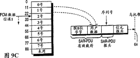
The data of each POTS channel all are constant octet stream usually, and the cycle is 125ms.These eight bit bytes are stored in 50 li in buffer continuously.The buffer of each POTS channel all has 94 eight bit byte positions, this is equivalent to two cells for full packing pattern (Fig. 9 A), for 22 partially filled patterns of eight bit byte (Fig. 9 B), this is equivalent to 4 cells, and for 11 partially filled patterns of eight bit byte (Fig. 9 C), this is equivalent to 8 cells.
The carrier cell (full packing) of 6.5.1 segmentation: 64kbps
When circuit simulation (CE) device 72 was operated in 64kbps carrier element pattern, buffer was configured to two zones, and there are 47 eight bit bytes (Fig. 9 A) in each zone.Cell of each Regional Representative---first zone (eight bit byte 0~46) representative is numbered the cell of even number, and other zone (eight bit byte 47+) representative is numbered the cell of odd number.CPU40 is by setting a dedicated bit and control each channel and start working being provided with in the register.The channel that uses single 64kbps carrier all is independent initialized.As long as the data from pcm interface have been filled up in zone, just produce a cell and send toward up direction.Owing to, therefore, when just ATM core 60 is sent the cell request, just produce cell only at the device of control Utopia interface 64 without any extra cell buffer.ATM core 60 is received a signal, and illustrating has a cell all set, just sends the cell request then at once, and in fact this signal refers to and be about to produce a cell.When a cell produces, just the PCM data of 47 eight bit bytes are inserted the SAR-PDU Payload, simultaneously a sequence number is put into the SAR-PDU header.
6.5.2 segmentation: 64kbps carrier cell (22 eight bit bytes)
When having adopted the 64kbps carrier cell of 22 eight bit bytes partially filled, buffer is configured to each 4 zone (Fig. 9 B) that 22 eight bit bytes are all arranged.As mentioned above, a cell is all represented in each zone (for example zone 1~4): first zone (eight bit byte 0~21) represents sequence number is 0 and 4 cell, second zone (eight bit byte 22~43) expression sequence number is 1 and 5 cell, the 3rd zone (eight bit byte 44~65) expression sequence number is 2 and 6 cell, and the 4th zone (eight bit byte 66~87) expression sequence number is 3 and 7 cell.Even here, CPU allows write buffer.When a cell areas is filled up data (22 eight bit bytes), just provide signal instruction and can produce a cell.The method that face is introduced in front of the production method of cell is the same, but only 22 eight bit bytes is put into the SAR-PDU Payload.25 remaining eight bit bytes are false eight bit bytes.
6.5.3 segmentation: 64kbps carrier cell (11 eight bit bytes)
When adopting the 64kbps carrier cell of partially filled 11 eight bit bytes, buffer has been configured to 8 zones, and each all has 11 eight bit bytes.The same in the pattern of front face, a cell is all represented in each zone.But in this case, each sequence number all has a unique zone.The CPU startup writes buffer, even because the less this point that makes of combinatorial delays is not crucial.Second kind of pattern that face is introduced in front of the generation of cell is the same, and difference only is that the number of false eight bit byte (36) is different.
6.5.4 handle several 64kbps carriers simultaneously
In order to handle two 64kbps channels simultaneously, 94 eight bit byte buffers must double, shown in Fig. 9 D.For the part that writes in buffer, this can not bring any difference.The channel that each channel all is independent of other stores.For the part that produces cell, each buffer all is seen as a different cell flow, and they are exactly cell flow.When channel 1 is about to produce a cell, just special 64 1 signals of business interface of giving.For channel 2, provide signal according to another signal.Business interface 64 sends the cell request respectively to two Channel Elementss.For the situation that 4 channels are arranged, need the buffer of 4 * 94 eight bit bytes, shown in Fig. 9 D.
6.5.5 the packing of non-structure E1/T1 frame
In ATM, the transmission of E1 (2048kbps) and T1 (1544kbps) all is structureless, that is to say, does not handle single 64kbps channel when packing data is produced the full packing cell.Because what use is serial line interface, therefore without any necessary align data.In this pattern, buffer is provided with according to Fig. 9 E.In this pattern, the data of filling in the buffer are more faster than n * 64kbps pattern, and this means does not have so strict requirement to the initialization that writes.
6.6 reorganization
For recombination function has been stipulated with the same buffer of fragmentation feature.Further, these buffers are identical with the configuration of fragmentation feature.
6.6.1 unpack
The same to unpacking of carrying out of different cells with packing process.Receive cell from business interface 64.If used several single 64kbps carriers, just isolate these channels with different enabling signals.When receiving a cell, just manage store user data (determining) with sequence number at the reserved area of buffer.Notify an end of read data simultaneously, like this it just can know be read last time after, whether data have write into this zone.This buffer is to read continuously with a kind of continuous order, and data flow is sent to pcm interface 32---channel of each buffer.Figure 10 explanation is unpacked to two partially filled single 64kbps carrier cells.
6.6.2 handle lose and misplug into cell
When circuit simulation (CE) device 72 is received a cell, just check the sequence number in the SAR-PDU header.If cell C
tThe cell C of front face
T-1Discontinuous, just it is discarded, not store user data.If next cell C
T+1Cell C
T-1Continuously, just think cell C
tMisplug into, regrouping process continues.If cell C
T+1With cell C
T-1Discontinuous, just think at cell C
T-1And C
T+1Between lost many cells.Even in this case, still continue regrouping process, be a correct cell even the result is it, also with cell C
tDiscard.Yet, can not store one may be misplug into cell because when using the full packing cell, two cells can only be put down in the space of buffer.Figure 11 has illustrated an example.
If reading the buffer areas that cell number is an odd number, and at this moment sequence number is that mispluging into cell of odd number arrives C
t, just pay(useful) load can not be deposited in the zone of just being read.Because buffer space is very little, can not insert buffer with the cell that the false data of advising previously replaces losing.But during at every turn with a cell Payload write buffer, all notify that end of read data.If reading last time to show without any sign later on writes a zone with a cell, a side of read data just produces the false data position (1s) of necessary amount.
Postpone to change (CDV) 6.6.3 handle cell
If cells all in the network all have identical delay, they just should occur with the accurate cycle.At this moment, the read data part can begin read buffer when first cell has arrived.In fact, some cell postpones longer (see figure 8), this means the data (overflowing under the data) that will read when a buffer areas is not also filled up data wherein.Therefore, when first cell arrived, the part of read data should postpone at the very start, can read each cell continuously in following period of time like this after cell is written into.In this situation, can buffer underflow not occur a little while and go out because of a cell is suddenly late.Can postpone to programme to extra CDV by CPU.
6.7 synchronously
For synchronous telephone signal stream, multiple business circuit 20 needs the network reference clock of a 8kHz.Utilize phase-locked loop (DPLL) to produce a clock signal, lock reference clock signal, in Figure 12 for the DL synchronization data transfer rate.When interface 32 is a pcm interface, oscillator frequency (f
Osc) must be 32.768MHz, the clock frequency (f of generation
Lck) must be 2.048MHz.The E1 interface too.But if use T
1, f
OscBe exactly 24.704MHz, f
LckBe exactly 1.544MHz.This oscillator is an external oscillator.
6.8 interface and clock signal
Circuit simulation (CE) device 72 links to each other with internal cpu bus 73 with interface 32, business interface 64.Circuit simulation (CE) device 72 is divided into two clock zones.The processing of ATM cell (distribute data between buffer and business interface 64) is to come synchronous with the clock signal (system clock) that business interface 64 distributes.On the other hand, the processing of phone data (distribute data between PCM/E1/T1 interface and buffer) is to come synchronous (seeing Figure 12) with the DPLL clock.
7.0 Utopia's buffer
Utopia's buffer 74 shown in Figure 13 is a buffer between the business interface (Utopia of inner branch interface) of ATM core 60 controls and the external business Utopia interface 34 of following its continuous external device (ED) control basically.Each direction of the internal buffer that Utopia's buffer is 74 li can store 2 cells.Outside Utopia interface 34 can be operated in the second layer or ground floor pattern, and the selection of pattern is being provided with at first by CPU40.In second layer pattern, also physical address must be set.Utopia's buffer 74 has three different clocks.Distribute data is synchronous by system clock between Utopia's buffer 74 and inner branch support interface (business interface 64).Distribute data is next synchronous by two independent clocks that are used to receive and dispatch between Utopia's buffer 74 and outside Utopia interface 34, and these two clock signals are all provided by outside Utopia interface 34.
8.0 ATMF25.6 transceiver
At down direction (shown in the arrow 150 among Fig. 2), ATMF transceiver 70
1, 70
2The cell of receiving is from business interface 64, is stored temporarily in after dark FIFO (first-in first-out) lining of two cells, all uses 25.6 MHz line 30
1, 30
2Transmit.At up direction (shown in the arrow 152 among Fig. 2), cell is from 25.6 Mbps lines 30
1, 30
2On receive that and be stored in the dark FIFO of two cells, ATM core 60 can therefrom read out them.The ATM 25.6 Mbps physical interfaces of atm forum have stipulated to depend on the sublayer of physical medium (PMD) and the function that (TC) sublayer is assembled in transmission.For descender provides the reference signal (with the same signal of DPLL of circuit simulation (CE) device 72) of a 8kHz, like this, just can on ATMF interface 30, send timing information.Descending clock signal branches away from an outside 32MHz oscillator.Extract in the upstream during up clock signal.Come processing between synchronization fifo and the business interface 64 with Utopia's clock signal (clock signal of system).
9.0CPU module
CPU module 71 is at (1) outer CPU bus 42 and (2) ATM core 60 and service apparatus 70
1, 70
2, distribute data between 72 and 74.CPU module 71 is handling interrupt also.The all functions that CPU module 71 is finished comprise the transaction to internal interface (for example bus 73), and are all synchronous with clock signal of system.
9.1 read-write is handled
The read-write that explanation CPU module 71 is carried out in Figure 15 is handled.When CPU40 carried out read-write operation to multiple business circuit 20, CPU module 71 detected a low transaction (low transaction) on chip selection signal (CS).Signal on 71 pairs of address buss of CPU module is decoded then, and selects signal to send to selected module (for example ATM core 60 or service apparatus 70 minimum several and the piece of address bus signal
1, 70
2, in 72 and 74 one).Bus 73 is a kind of BDB Bi-directional Data Bus, when needing read and write, it is become two independently buses.When inner read-write operation finishes, just transmit confirmation signal and illustrate with data.Since it is synchronous that read-write operation is come by system clock, therefore this timing mode depends on frequency.
9.2 Interrupt Process
Each module of multiple business circuit 20 all provides at least one sign to CPU module 71.Sign is stored in the status register of CPU module 71 management.In the status register one changes to high office from low transaction and comprehends and cause sending a terminal request (IREQ) to CPU40.Data in the CPU40 read status register or when receiving interruption acknowledge signal (IACK) are just abandoned this interrupt requests.By with the position, a certain position in the mask register, can refuse interrupt requests.Figure 16 illustrates the structure of Interrupt Process.
1. the following incident of 20 li in multiple business circuit is relevant with corresponding Interrupt Process sign:
Descending CPU read buffer in ATM core 60 stores a complete cell (seeing Fig. 2 A) for 106 li.
2. the buffer 136 in the uplink CP U of ATM core 60 read buffer group 136
1In store a complete cell (seeing Fig. 2 B).
3. the buffer 136 in the uplink CP U of ATM core 60 read buffer group 136
2In store a complete cell (seeing Fig. 2 B).
4. the buffer 136 in the uplink CP U of ATM core 60 read buffer group 136
3In store a complete cell (seeing Fig. 2 B).
5. lose synchronous event in the channel 1 of circuit simulation (CE) device 72, perhaps buffer overflow or under overflow.
6. lose synchronous event in the channel 2 of circuit simulation (CE) device 72, perhaps buffer overflow or under overflow.
7. lose synchronous event in the channel 3 of circuit simulation (CE) device 72, perhaps buffer overflow or under overflow.
8. lose synchronous event in the channel 4 of circuit simulation (CE) device 72, perhaps buffer overflow or under overflow.
10.0ATM the VPI/VCI of core table
As mentioned above, demultiplexer and decoder 102 and downstream multiplexer 104 adopt the VPI/VCI table that CPU40 is provided with.What Figure 17 A illustrated is the VPI/VCI table of demultiplexer and decoder 102; What Figure 17 B illustrated is the VPI/VCI table of downstream multiplexer 104.
10.1 the VPI/VCI of descending demultiplexer and decoder
Shown in Figure 17 A, demultiplexer and decoder 102 have a set VPI/VCI Identification Lists 102-10 and the VPI/VCI of branch to decipher and purpose face of land 102-20.The cell of input demultiplexer and decoder 102 has certain header information, is used for validity comparator 102-30 and a VPI/VCI register 102-40.This certain header information comprises low four (LSB) and the high eight-bit of VCI of the VPI of header.In validity comparator 102-30, header is compared with a filter value that is stored in VPI register 102-32.If header information is effective, just useful signal is mail to controller 102-50.
Demultiplexer and decoder 102 are attempted to find out with the value that is stored in the header information coupling among the VPI/VCI register 102-4 in set VPI/VCI Identification Lists 102-10.Shown in Figure 17 A, in fact VPI/VCI Identification Lists 102-10 comprises four RAMS 102-10 (1)~(4).The readout window of each links to each other with first some in comparator 102-60 (1)~(4) input port in RAMS102-10 (1)~(4).The value that stores among the VPI/VCI register 102-40 to receive is linked up in second input port of each in comparator 102-60 (1)~(4).In RAMS102-10 (1)~(4) each all has 32 positions (32 * 4=128 byte RAM).When demultiplexer and decoder 102 are received a new cell, deposit header information in VPI/VCI register 102-40, check first position of all four RAM this moment simultaneously.That is to say the value of four first positions of RAM is exported to corresponding comparator 102-60, thereby whether the value of judging first position follows the header information unanimity of receiving.If inequality,, go on like this up to finding identical value with regard to checking second position of all four RAM in the same way simultaneously.All four needed maximum durations of RAM of search are 32 clock cycle like this.
When finding the value of coupling, determine an index value, be used to visit the VPI/VCI of branch decoding and purpose face of land 102-20, and leave demultiplexer and new header of decoder 102 preparations for this cell in view of the above.Shown in Figure 17 A, index value has two parts.First is used for an address or a value that obtains identical value from four RAM.Second portion is one the 2 bit wide addresses of changing acquisition when finding identical value from four output signals of four comparator 102-60.The reference address of this 2 bit wide obtains from converter 102-70, and its input links to each other with the output of each among the comparator 102-60.Index value points to the position of the VPI/VCI of branch decoding and purpose face of land 102-20, can utilize it to obtain new header and destination value.The new header of branch's Route Selection has four and eight of VCI of VPI.The destination value is one four place value of explanation branch's Utopia's device or CPU40 or descending loop-back buffer 108.
Therefore, as mentioned above, demultiplexer and decoder 102 have one group of integrated ram table, and these tables are provided with by CPU 40.From the perspective view of CPU40 as can be known, all there is a unique address each position of VPI/VCI table.Find an address of VPI/VCI table to have one during with the identical VPI/VCI of the VPI/VCI of input cell header, just there are new destination (for example one of CPU40, loop-back buffer 108 or service apparatus) and new VPI/VCI in the relevant position in the VPI/VCI table.
If the VCI territory in the loopback table is reset (VCI=0), just think that it is a kind of VPC that this ATM connects, the VCI that this means cell header can be an arbitrary value.At this moment, have only VPI necessary identical, do not decipher VCI.It is very flexible to utilize VCI=0 to define the method for VPC, because the undefined value that ATM connects during VCI=0 that is to say at 20 li cells that VCI=0 can not occur of multiple business circuit.When idle cell and physics OAM have VCI=0, just in modulator-demodulator, these cells are picked out.Except indicate VPC with VCI=0, the state of VPC can also illustrate with other in the loopback table.
10.2 the VPI/VCI of upstream multiplexer table
Shown in Figure 17 B, up demultiplexer and decoder 122 have the VPI/VCI of a branch Identification Lists 122-10, gather VPI/VCI decoding table and purpose face of land 122-20 for one, and an EPD state table 122-25.The cell that enters up demultiplexer and decoder 122 has specific header information and corresponding Utopia's address value (4), is stored in the VPI/VCI register 122-40.This specific header information comprises low four (LSB) and the high eight-bit of VCI of header VPI.
As demultiplexer and decoder 102, up demultiplexer and decoder 122 are attempted seeking the header information and the Utopia address that store in the VPI/VCI register 122-40 and are followed the value of mating in the VPI/VCI of the branch Identification Lists 122-10.Shown in Figure 17 B, VPI/VCI Identification Lists 122-10 comprises four RAMS 122-10 (1)~(4).In RAMS 122-10 (1)~(4) each all has a readout window to link to each other with one first input port corresponding in comparator 122-60 (1)~(4).Second input port of each couples together and is stored in value in the VPI/VCI register 122-40 with reception in comparator 122-60 (1)~(4).When up demultiplexer and decoder 122 are received a new cell, deposit header information and Utopia address in VPI/VCI register 122-40, in this case, the value that in RAMS 122-10, is complementary with the used same procedure search of the RAMS 102-10 of front.
When finding the value of being complementary, determine that an index value is with visiting set VPI/VCI decoding and purpose face of land 122-20 and (when it is used) EPD table 122-125.In the set VPI/VCI decoding and purpose face of land 122-20 of having worked out index, for the cell that will leave up demultiplexer and decoder 122 obtains a new header.The same with decoder 102 with demultiplexer, as shown in figure 17, this index value has two parts.First is used for from four RAMS122-10 one address or value that obtains identical value.Second portion is when obtaining this value of being complementary, from the address of 2 bit wides of the conversion acquisition of four output signals of four comparator 122-60.The address of this 2 bit wide obtains from converter 122-70, and this converter is linked to each other with each the output among the comparator 122-60 by some inputs.This index value points to certain position among set VPI/VCI decoding and the purpose face of land 122-20, from obtaining new header here.The new header of this branch's Route Selection has four VPI and eight VCI.
VPI filter register 102-32 was used for before cell sends to the set interface, a new vpi value (high eight-bit) is inserted the header of cell, in downstream data flow, only accept the set cell of (only broadcasting cell) its VPI corresponding to register 102-32, after their decoding, the high eight-bit of VPI is resetted.In upstream, only accept the null branch of VPI (high eight-bit) cell, after their decoding, the value of register 102-32 is inserted VPI (high eight-bit).
For each position (address) among set VPI/VCI decoding and the purpose face of land 122-20, the position of a correspondence is arranged all in EPD table 122-25.This EPD table 122-25 comprises that each ATM connects the information that need be used for handling EPD.Just use this EPD table 122-25 when only the selection position of an EPD in VPI/VCI Identification Lists 122-10 is set.
11.0 postscript
Therefore the core of ATM core 60 is multiple business circuit 20.ATM core 60 has integrated loop-back buffer, cpu buffer and quality of service buffer.More advantageously, ATM core 60 is very flexible, and its structure and the course of work do not rely on Utopia of branch interface, and for example business interface 64, the type of the service apparatus that is connected.
The a plurality of physics Utopia interfaces that business interface 64 provides can also integrated future business (for example, AAL5 SAR and Ethernet).In addition, though eight channels are arranged in embodiment, ATM core 60 can expand to more channel (for example 16 channels).
Multiple business circuit 20 of the present invention is a kind of integrated circuits that all are based on hardware basically.Therefore, this multiple business circuit 20 is followed based on the circuit of processor and is compared many advantages that other is arranged, for example higher data transfer rate and lower power consumption.
Though introduce when of the present invention, adopted the optimum implementation of thinking the most practical at present, obviously, and the embodiment that the present invention is not limited to announce, on the contrary, it has also covered included various modifications and the equivalence of claims.For example, can add CPU40 for 20 li at the multiple business circuit.
Table 1 is by the example of the ATM connection of NT
| ATM connects | VPI/VCI gathers side | VPI/VCI branch side | The QoS level |
| CE channel 1 (VCC) | VPI 1/43 | CE1_fix | QoS1 |
| CE channel 2 (VCC) | VPI 1/44 | CE2_fix | QoS1 |
| Professional Utopia (VCC) | VPI 1/48 | 0/35 | QoS2 |
| ATM#1(VCC) | VPI 1/55 | 0/35 | QoS3 |
| ATM#1(VPC) | VPI 1/- | 1/- | QoS3 |
| ATM#2(VCC) | VPI 1/58 | 0/35 | QoS3 |
| CPU<- | - | 0/3 | - |
| CPU<- | - | 0/35 | - |
| CPU<-set, the end-to-end CAM of F4 | VPI 1/4 | - | QoS4 |
| CPU<-set, signaling (VCC) | VPI 1/33 | - | QoS4 |
| CPU<-set, signaling (VPC) | VPI 2/- | - | QoS4 |
Table 2 is to Utopia's layer 2 interface of modem/transceiver
| Signal name | Type | Width | | |
| TX_DATA | Output | |||
| 8 | Send data. | |||
| | Output | 1 | The tranmitting data register signal. | |
| | Output | 1 | Start and send eight bit | |
| TX_SOC | Output | |||
| 1 | Send the beginning of | |||
| TX_CLAV | Input | |||
| 1 | Send cell free space signal. | |||
| | Output | 5 | Send the address. | |
| | Input | 8 | Receive data. | |
| | Output | 1 | The receive clock signal. | |
| | Output | 1 | Start and receive eight bit | |
| RX_SOC | Input | |||
| 1 | Receive the beginning of | |||
| RX_CLAV | Input | |||
| 1 | Receive cell. | |||
| | Output | 5 | Receiver address. |
Table 3 PCM and E1/T1 Interface
| Signal name | Type | Width | | |
| TxCLK | Output | |||
| 1 | The tranmitting data register signal, 2048 or 1544kHz. | |||
| | Input | 1 | The receive clock signal, 2048 or 1544kHz.Be E1/T1 only. | |
| | Output | 1 | Send data. | |
| | Input | 1 | Receive data. | |
| | Output | 1 | Beginning PCM frame. | |
| | Output | 4 | The data of each channel are all effective. |
Table 4 ATMF interface
| Signal name | Type | Width | | |
| TxD | Output | |||
| 2 | Difference sends data. | |||
| | Input | 2 | The differential received data. | |
| | Bidir | 2 | The external filter of equalizer. | |
| | Bidir | 2 | The external filter of PLL. | |
| | Bidir | 4 | The analog signal power supply. | |
| | Bidir | 4 | Analog signal ground. |
Table 5 external business Utopia interface
| Signal name | Type | Width | | |
| TX_DATA | Input | |||
| 8 | Send data. | |||
| | Input | 1 | The tranmitting data register signal. | |
| | Input | 1 | Start and send eight bit | |
| TX_SOC | Input | |||
| 1 | Send the beginning of | |||
| TX_CLAV | Output | |||
| 1 | Send cell free space signal. | |||
| | Input | 5 | Send the address. | |
| | Output | 8 | Receive data. | |
| | Input | 1 | The receive clock signal. | |
| | Input | 1 | Start and receive eight bit | |
| RX_SOC | Output | |||
| 1 | Receive the beginning of | |||
| RX_CLAV | Output | |||
| 1 | Receive cell. | |||
| | Input | 5 | Receiver address. |
Table 6 outer CPU interface
| Signal name | Type | Width | | |
| CS | Input | |||
| 1 | The sheet choosing | |||
| R/ | Input | 1 | Start read/write | |
| | Input | 12 | Address | |
| DATA | Bidir | |||
| 16 | Data/address | |||
| IREQ | Output | |||
| 1 | Interrupt requests | |||
| DTACK* | | 1 | Transfer of data is confirmed | |
| IACK* | | 1 | Interruption acknowledge | |
| OE* | | 1 | Start output | |
| BMODE* | | 1 | Mode bus (16/8) | |
| BSEL* | | 1 | Byte is chosen |
Claims (14)
1. one kind of multiple service circuits are used for receiving ATM cell on the external interface from modem/transceiver, control this multiple business circuit with a processor, and this multiple business circuit comprises:
Handle a plurality of service apparatus of different telecommunication businesses;
Be connected a multiplexer/demultiplexer core between a plurality of service apparatus and the external interface, this core has
-one downlink side, be used for transmitting cell from external interface to service apparatus, also have a upstream side to be used for transmitting cell from service apparatus to external interface, this downlink side has a descending demultiplexer and a downstream multiplexer, upstream side has a upstream multiplexer and a up demultiplexer
-one descending loop-back buffer is used to store the cell that goes from downlink side toward upstream side;
-one up loop-back buffer is used to store the cell that goes from upstream side toward downlink side;
-wherein descending demultiplexer is used for the cell from external interface is sent to this three of an input of descending loop-back buffer, processor and downstream multiplexer;
-wherein downstream multiplexer is used to obtain the cell from descending demultiplexer, up loop-back buffer and processor, and is transferred to service apparatus;
-wherein up demultiplexer is used for sending the cell from service apparatus and processor to buffering area between up loop-back buffer, processor and up demultiplexer and the upstream multiplexer one; With
-wherein upstream multiplexer is used for obtaining cell from one of buffering area and descending loop-back buffer, and passes to external interface.
2. the device of claim 1, descending demultiplexer wherein and downstream multiplexer can both be worked simultaneously independently, remove and leave no choice but send the cell of descending demultiplexer to downstream multiplexer.
3. the device of claim 2, wherein having a service apparatus at least is a kind of ATMF transceiver.
4. the device of claim 2, wherein having a service apparatus at least is with a continuous a kind of simulator in (3) T1 interfaces of (2) E1 interfaces of (1) pcm interface.
5. the device of claim 4, simulator wherein has a buffer, and is with the data or the full packing of a channel, perhaps partially filled.
6. the device of claim 4, simulator wherein has a buffer, and is with the data or the full packing of all channels, perhaps partially filled.
7. the device of claim 2, wherein having a service apparatus at least is a kind of Utopia second layer device.
8. the device of claim 2, cell wherein is an ATM cell.
9. the device of claim 2, Utopia's second layer divides support interface that these a plurality of service apparatus are linked to each other with multiplexer/demultiplexer core.
10. the device of claim 2, multiple business circuit wherein is an integrated circuit (IC) chip.
11. the device of claim 2, wherein whole multiple business circuit is made with hardware.
12. one kind of multiple service circuits are used for receiving ATM cell on the external interface from modem/transceiver, control this multiple business circuit with a processor, and this multiple business circuit is made chip piece, comprising:
Handle a plurality of service apparatus of different telecommunication businesses;
Be connected a multiplexer/demultiplexer core between a plurality of service apparatus and the external interface;
This core is followed a continuous internal interface of a plurality of external device (ED)s; With
Wherein at down direction, this core will be sent to one of a plurality of service apparatus by internal interface from the cell of external interface, be sent to processor and external interface;
Wherein at up direction, this core will send one of external interface, processor and internal interface to by internal interface and processor from the cell of a plurality of service apparatus.
13. the device of claim 12, wherein having an external interface and internal interface at least is a kind of Utopia layer 2 interface.
14. the device of claim 12, whole multiple business circuit is wherein made with hardware.
Applications Claiming Priority (3)
| Application Number | Priority Date | Filing Date | Title |
|---|---|---|---|
| US09/009,535 | 1998-01-20 | ||
| US09/009,535 US6256308B1 (en) | 1998-01-20 | 1998-01-20 | Multi-service circuit for telecommunications |
| US09/009535 | 1998-01-20 |
Publications (2)
| Publication Number | Publication Date |
|---|---|
| CN1257635A CN1257635A (en) | 2000-06-21 |
| CN1126424C true CN1126424C (en) | 2003-10-29 |
Family
ID=21738256
Family Applications (1)
| Application Number | Title | Priority Date | Filing Date |
|---|---|---|---|
| CN98805279A Expired - Fee Related CN1126424C (en) | 1998-01-20 | 1998-12-30 | Multi-service circuit for telecommunication |
Country Status (10)
| Country | Link |
|---|---|
| US (2) | US6256308B1 (en) |
| EP (1) | EP0968623A1 (en) |
| JP (1) | JP3342500B2 (en) |
| KR (1) | KR100683990B1 (en) |
| CN (1) | CN1126424C (en) |
| AU (1) | AU2444299A (en) |
| CA (1) | CA2284175C (en) |
| HK (1) | HK1027934A1 (en) |
| TW (1) | TW466854B (en) |
| WO (1) | WO1999037117A1 (en) |
Families Citing this family (24)
| Publication number | Priority date | Publication date | Assignee | Title |
|---|---|---|---|---|
| KR19990059282A (en) * | 1997-12-30 | 1999-07-26 | 서평원 | AT matching device of ATM switch |
| US6256308B1 (en) * | 1998-01-20 | 2001-07-03 | Telefonaktiebolaget Lm Ericsson | Multi-service circuit for telecommunications |
| US7227837B1 (en) | 1998-04-30 | 2007-06-05 | At&T Labs, Inc. | Fault tolerant virtual tandem switch |
| US6169735B1 (en) * | 1998-04-30 | 2001-01-02 | Sbc Technology Resources, Inc. | ATM-based distributed virtual tandem switching system |
| US6700872B1 (en) * | 1998-12-11 | 2004-03-02 | Cisco Technology, Inc. | Method and system for testing a utopia network element |
| CA2290304C (en) * | 1998-12-23 | 2009-03-17 | Nortel Networks Corporation | Direct end-office atm trunking |
| KR20020035650A (en) * | 1999-10-05 | 2002-05-13 | 추후제출 | Components for providing voice and/or data service |
| GB2355883B (en) * | 1999-10-27 | 2003-10-08 | Mitel Corp | Transmission rate control system for ATM cells |
| US6343065B1 (en) * | 2000-01-20 | 2002-01-29 | Sbc Technology Resources, Inc. | System and method of measurement-based adaptive caching of virtual connections |
| AU2001260529A1 (en) * | 2000-05-31 | 2001-12-11 | Adc Telecommunications Israel Ltd. | Non intrusive self test capability in the utopia level two bus |
| KR100336593B1 (en) * | 2000-06-14 | 2002-05-16 | 박종섭 | Interface between UTOPIA level 2 and UTOPIA level 1 in ATM mutiplexing/demultiplexing assembly |
| US20020136220A1 (en) * | 2000-10-02 | 2002-09-26 | Shakuntala Anjanaiah | Apparatus and method for an interface unit for data transfer between data processing units in the asynchronous transfer mode and in the I/O mode |
| US20020181441A1 (en) * | 2001-04-24 | 2002-12-05 | Alcatel, Societe Anonyme | Facilitating inverse multiplexing over asynchronous transfer mode via communication links having disparate data transmission rates |
| US6850526B2 (en) * | 2001-07-06 | 2005-02-01 | Transwitch Corporation | Methods and apparatus for extending the transmission range of UTOPIA interfaces and UTOPIA packet interfaces |
| US7646782B1 (en) | 2001-07-30 | 2010-01-12 | Primrose Donald R | Data link/physical layer packet buffering and flushing |
| US7415031B2 (en) * | 2001-07-30 | 2008-08-19 | Null Networks Llc | Data link/physical layer packet diversion and insertion |
| KR20030019823A (en) * | 2001-08-31 | 2003-03-07 | 주식회사 현대시스콤 | Apparatus and method for interfacing between block in ATM system |
| KR100494556B1 (en) * | 2002-07-13 | 2005-06-10 | 한국전자통신연구원 | Asynchronous transfer mode-passive optical network slave device and method for transferring/receiving thereof |
| DE10324603A1 (en) * | 2003-05-30 | 2004-12-23 | Siemens Ag | Method for forwarding IP packets to an external control component of a network node |
| US7564381B1 (en) * | 2004-02-16 | 2009-07-21 | Cisco Technology, Inc. | System and method for code-based compression in a communications environment |
| CN101626346B (en) * | 2009-08-03 | 2011-12-07 | 中兴通讯股份有限公司 | Method and device for restoring self-adaptive clock |
| US10426424B2 (en) | 2017-11-21 | 2019-10-01 | General Electric Company | System and method for generating and performing imaging protocol simulations |
| KR102375556B1 (en) * | 2019-04-30 | 2022-03-17 | 삼성전자주식회사 | Structure of Hinge and electronic device including the same |
| CN112153178A (en) * | 2019-06-27 | 2020-12-29 | 华为技术有限公司 | Rotating shaft mechanism and foldable mobile terminal |
Family Cites Families (38)
| Publication number | Priority date | Publication date | Assignee | Title |
|---|---|---|---|---|
| DE3742939A1 (en) | 1987-12-18 | 1989-07-06 | Standard Elektrik Lorenz Ag | METHOD FOR HYBRID PACKING AND DEVICES THEREFOR |
| JPH04138739A (en) | 1990-09-28 | 1992-05-13 | Toshiba Corp | Communication control system using asynchronous transmission mode network |
| EP0510290B1 (en) | 1991-04-22 | 1997-02-05 | International Business Machines Corporation | Collision-free insertion and removal of circuit-switched channels in a packet-switched transmission structure |
| JP3051210B2 (en) * | 1991-08-05 | 2000-06-12 | 富士通株式会社 | Test method for ATM multiplex transmission equipment |
| SE470002B (en) | 1992-03-13 | 1993-10-18 | Ellemtel Utvecklings Ab | A method for preventing the transmission of data packets with a higher intensity than a predetermined value for the channel and a device for carrying out the method on one of a number of channels on a common transmission line |
| WO1993020634A1 (en) | 1992-04-06 | 1993-10-14 | Northern Telecom Limited | Method for atm switch core interface |
| JP2829807B2 (en) | 1992-07-10 | 1998-12-02 | 松下電器産業株式会社 | Cell delay addition circuit |
| CA2104753C (en) | 1992-10-29 | 1999-02-16 | Kotikalapudi Sriram | Bandwidth allocation, transmission scheduling, and congestion avoidance in broadband atm networks |
| MX9308193A (en) | 1993-01-29 | 1995-01-31 | Ericsson Telefon Ab L M | CONTROLLED ACCESS ATM SWITCH. |
| US5396492A (en) | 1993-04-28 | 1995-03-07 | At&T Corp. | Method and apparatus for adaptive clock recovery |
| US5370362A (en) * | 1993-10-15 | 1994-12-06 | Abb Vetco Gray Inc. | Gate valve |
| DE4343720C1 (en) | 1993-12-21 | 1995-06-14 | Siemens Ag | Method for transmitting digital signals in an ATM communication network |
| JP3405800B2 (en) | 1994-03-16 | 2003-05-12 | 富士通株式会社 | ATM-based variable-length cell transfer system, ATM-based variable-length cell switch, and ATM-based variable-length cell switch |
| EP0677938A1 (en) | 1994-04-14 | 1995-10-18 | ALCATEL BELL Naamloze Vennootschap | Signal coupler |
| US5526344A (en) * | 1994-04-15 | 1996-06-11 | Dsc Communications Corporation | Multi-service switch for a telecommunications network |
| JPH07297830A (en) * | 1994-04-21 | 1995-11-10 | Mitsubishi Electric Corp | Multiplexer, non-multiplexer, switching device, and network adapter |
| JPH07307738A (en) | 1994-05-13 | 1995-11-21 | Mitsubishi Electric Corp | Protocol processor |
| GB2291562B (en) | 1994-05-21 | 1998-09-23 | Northern Telecom Ltd | Communications system |
| GB9413716D0 (en) * | 1994-07-07 | 1994-08-24 | Plessey Telecomm | Telecommunications network |
| US5619500A (en) * | 1994-09-01 | 1997-04-08 | Digital Link Corporation | ATM network interface |
| JP2571025B2 (en) | 1994-10-13 | 1997-01-16 | 日本電気株式会社 | Optical termination node in the network |
| US5481544A (en) | 1994-10-17 | 1996-01-02 | At&T Corp. | Multi-channel broadband adaptation processing |
| JP2817768B2 (en) | 1994-12-27 | 1998-10-30 | 三菱電機株式会社 | Ring type ATM network system |
| US5533009A (en) | 1995-02-03 | 1996-07-02 | Bell Communications Research, Inc. | Bandwidth management and access control for an ATM network |
| US5608731A (en) | 1995-03-31 | 1997-03-04 | Transwitch Corporation | Closed loop clock recovery for synchronous residual time stamp |
| US5668798A (en) | 1995-04-05 | 1997-09-16 | International Business Machines Corporation | Multiplexed TC sublayer for ATM switch |
| US5563885A (en) | 1995-05-24 | 1996-10-08 | Loral Fairchild Corporation | Method and system for processing multiple channel data |
| US6002667A (en) | 1995-07-19 | 1999-12-14 | Fujitsu Network Communications, Inc. | Minimum guaranteed cell rate method and apparatus |
| US5734652A (en) | 1995-09-27 | 1998-03-31 | Microsoft Corporation | ATM extended autoregistration and VPI/VCI assignment in a hybrid fiber-coax cable network |
| US5982772A (en) * | 1995-11-06 | 1999-11-09 | Sun Microsystems, Inc. | Cell interface block partitioning for segmentation and re-assembly engine |
| US5757771A (en) | 1995-11-14 | 1998-05-26 | Yurie Systems, Inc. | Queue management to serve variable and constant bit rate traffic at multiple quality of service levels in a ATM switch |
| US5805591A (en) * | 1996-02-28 | 1998-09-08 | Ericsson Raynet | Subscriber network interface |
| US5822321A (en) * | 1996-04-10 | 1998-10-13 | Telefonaktiebolaget Lm Ericsson | Minicell segmentation and reassembly |
| JPH10178451A (en) * | 1996-10-17 | 1998-06-30 | Fujitsu Ltd | Hybrid exchange, exchange, and method for re-assignment of stm data in the exchanges. |
| US5889773A (en) * | 1996-11-27 | 1999-03-30 | Alcatel Usa Sourcing, L.P. | Method and apparatus for placing time division multiplexed telephony traffic into an asynchronous transfer mode format |
| JP2001519121A (en) | 1997-04-04 | 2001-10-16 | アセンド コミュニケーションズ インコーポレイテッド | High-speed packet scheduling method and apparatus |
| US6118777A (en) * | 1997-10-27 | 2000-09-12 | Nortel Networks Corporation | System and method for providing competing local exchange carriers unbundled access to subscriber access lines |
| US6256308B1 (en) * | 1998-01-20 | 2001-07-03 | Telefonaktiebolaget Lm Ericsson | Multi-service circuit for telecommunications |
-
1998
- 1998-01-20 US US09/009,535 patent/US6256308B1/en not_active Expired - Lifetime
- 1998-10-12 TW TW087116890A patent/TW466854B/en not_active IP Right Cessation
- 1998-12-30 CA CA002284175A patent/CA2284175C/en not_active Expired - Lifetime
- 1998-12-30 CN CN98805279A patent/CN1126424C/en not_active Expired - Fee Related
- 1998-12-30 EP EP98966721A patent/EP0968623A1/en not_active Withdrawn
- 1998-12-30 KR KR1019997008598A patent/KR100683990B1/en not_active IP Right Cessation
- 1998-12-30 AU AU24442/99A patent/AU2444299A/en not_active Abandoned
- 1998-12-30 WO PCT/SE1998/002466 patent/WO1999037117A1/en active IP Right Grant
- 1998-12-30 JP JP53710299A patent/JP3342500B2/en not_active Expired - Fee Related
-
2000
- 2000-11-03 HK HK00107026A patent/HK1027934A1/en not_active IP Right Cessation
-
2001
- 2001-05-02 US US09/846,368 patent/US20010036188A1/en not_active Abandoned
Also Published As
| Publication number | Publication date |
|---|---|
| CA2284175A1 (en) | 1999-07-22 |
| KR100683990B1 (en) | 2007-02-20 |
| HK1027934A1 (en) | 2001-01-23 |
| WO1999037117A1 (en) | 1999-07-22 |
| JP3342500B2 (en) | 2002-11-11 |
| US6256308B1 (en) | 2001-07-03 |
| US20010036188A1 (en) | 2001-11-01 |
| AU2444299A (en) | 1999-08-02 |
| CN1257635A (en) | 2000-06-21 |
| CA2284175C (en) | 2006-10-10 |
| TW466854B (en) | 2001-12-01 |
| JP2000513546A (en) | 2000-10-10 |
| EP0968623A1 (en) | 2000-01-05 |
| KR20010005539A (en) | 2001-01-15 |
Similar Documents
| Publication | Publication Date | Title |
|---|---|---|
| CN1126424C (en) | Multi-service circuit for telecommunication | |
| CN1166247C (en) | Interconnect network for operation within communication node | |
| US6879590B2 (en) | Methods, apparatuses and systems facilitating aggregation of physical links into logical link | |
| AU688523B2 (en) | Method and switch node for switching STM cells in a circuit emulated ATM switch | |
| EP1078550B1 (en) | ADAPTIVE SCHEDULING METHOD AND APPARATUS TO SERVICE MULTILEVEL QoS IN AAL2 | |
| JPH06268665A (en) | Atm multiplexer | |
| CN1338837A (en) | Device, method and system for transmitting frames | |
| JP2002064587A (en) | Protocol terminating device | |
| EP0874530A1 (en) | Serial data transmission of variable length mini packets using statistical multiplexing | |
| CN1623302A (en) | ATM-port-module with integrated Ethernet switch interface | |
| US20020154629A1 (en) | Integrated PMP-radio and DSL multiplexer and method for using the same | |
| CN1111981C (en) | Mobile communication system having ATM-based connecting scheme | |
| CN1367969A (en) | Artificial line exchanging system and method, and sender-receiver-side transmitters for said system | |
| JPH1065681A (en) | Multiplex device | |
| US8559440B2 (en) | Merging multiple network data flows | |
| CN1677960A (en) | Method for switching ATM, TDM and packet data through a single communications switch | |
| JP2000196646A (en) | Band allocating method and band allocation transmission system | |
| CN1135790C (en) | ATM cell switching system | |
| CN1169326C (en) | ATM switching apparatus and method thereof | |
| JP3679249B2 (en) | ATM cell multiplexer | |
| CN1152529C (en) | Device and method for recovery of abnormal control cell in user unit | |
| US20020126700A1 (en) | Transmission techniques using universal data link protocol | |
| CN1273745A (en) | Distribution system | |
| CN1665216A (en) | Method and apparatus for continuous cell transmitting in ATM communication network | |
| WO2001010087A1 (en) | Scheduling with different time intervals |
Legal Events
| Date | Code | Title | Description |
|---|---|---|---|
| C06 | Publication | ||
| PB01 | Publication | ||
| C10 | Entry into substantive examination | ||
| SE01 | Entry into force of request for substantive examination | ||
| C14 | Grant of patent or utility model | ||
| GR01 | Patent grant | ||
| REG | Reference to a national code |
Ref country code: HK Ref legal event code: GR Ref document number: 1064161 Country of ref document: HK |
|
| CF01 | Termination of patent right due to non-payment of annual fee |
Granted publication date: 20031029 Termination date: 20141230 |
|
| EXPY | Termination of patent right or utility model |