CN112424695A - Metrology apparatus and method for determining a characteristic relating to one or more structures on a substrate - Google Patents
Metrology apparatus and method for determining a characteristic relating to one or more structures on a substrate Download PDFInfo
- Publication number
- CN112424695A CN112424695A CN201980047739.9A CN201980047739A CN112424695A CN 112424695 A CN112424695 A CN 112424695A CN 201980047739 A CN201980047739 A CN 201980047739A CN 112424695 A CN112424695 A CN 112424695A
- Authority
- CN
- China
- Prior art keywords
- substrate
- feature
- modified
- features
- focus
- Prior art date
- Legal status (The legal status is an assumption and is not a legal conclusion. Google has not performed a legal analysis and makes no representation as to the accuracy of the status listed.)
- Pending
Links
- 239000000758 substrate Substances 0.000 title claims abstract description 191
- 238000000034 method Methods 0.000 title claims abstract description 114
- 238000000059 patterning Methods 0.000 claims abstract description 58
- 230000008569 process Effects 0.000 claims abstract description 38
- 230000015572 biosynthetic process Effects 0.000 claims abstract description 23
- 238000005259 measurement Methods 0.000 claims description 50
- 238000001459 lithography Methods 0.000 claims description 13
- 230000001419 dependent effect Effects 0.000 claims description 7
- 238000004590 computer program Methods 0.000 claims description 3
- 230000005855 radiation Effects 0.000 description 39
- 238000005286 illumination Methods 0.000 description 23
- 230000006870 function Effects 0.000 description 20
- 238000007689 inspection Methods 0.000 description 16
- 230000003287 optical effect Effects 0.000 description 16
- 238000004519 manufacturing process Methods 0.000 description 13
- 210000001747 pupil Anatomy 0.000 description 11
- 238000013461 design Methods 0.000 description 8
- 238000012986 modification Methods 0.000 description 8
- 230000004048 modification Effects 0.000 description 8
- 235000012431 wafers Nutrition 0.000 description 8
- 238000012937 correction Methods 0.000 description 7
- 229920002120 photoresistant polymer Polymers 0.000 description 6
- 238000012545 processing Methods 0.000 description 6
- 238000001228 spectrum Methods 0.000 description 6
- 230000007547 defect Effects 0.000 description 5
- 238000005516 engineering process Methods 0.000 description 5
- 238000005530 etching Methods 0.000 description 5
- 238000003491 array Methods 0.000 description 4
- 238000007639 printing Methods 0.000 description 4
- 238000010586 diagram Methods 0.000 description 3
- 238000009826 distribution Methods 0.000 description 3
- 238000007654 immersion Methods 0.000 description 3
- 239000007788 liquid Substances 0.000 description 3
- 238000000691 measurement method Methods 0.000 description 3
- 238000004088 simulation Methods 0.000 description 3
- 102100029469 WD repeat and HMG-box DNA-binding protein 1 Human genes 0.000 description 2
- 101710097421 WD repeat and HMG-box DNA-binding protein 1 Proteins 0.000 description 2
- 238000013459 approach Methods 0.000 description 2
- 238000004140 cleaning Methods 0.000 description 2
- 230000008021 deposition Effects 0.000 description 2
- 230000000694 effects Effects 0.000 description 2
- 230000005670 electromagnetic radiation Effects 0.000 description 2
- 230000003993 interaction Effects 0.000 description 2
- 239000000463 material Substances 0.000 description 2
- 230000015654 memory Effects 0.000 description 2
- 238000012544 monitoring process Methods 0.000 description 2
- 238000005457 optimization Methods 0.000 description 2
- 238000004886 process control Methods 0.000 description 2
- 239000004065 semiconductor Substances 0.000 description 2
- 238000012360 testing method Methods 0.000 description 2
- 229910052721 tungsten Inorganic materials 0.000 description 2
- 238000012795 verification Methods 0.000 description 2
- 238000004458 analytical method Methods 0.000 description 1
- 238000004364 calculation method Methods 0.000 description 1
- 230000001010 compromised effect Effects 0.000 description 1
- 238000001816 cooling Methods 0.000 description 1
- 238000001514 detection method Methods 0.000 description 1
- 238000011161 development Methods 0.000 description 1
- 230000009977 dual effect Effects 0.000 description 1
- 238000001914 filtration Methods 0.000 description 1
- 238000000671 immersion lithography Methods 0.000 description 1
- 238000012417 linear regression Methods 0.000 description 1
- 239000004973 liquid crystal related substance Substances 0.000 description 1
- 230000005381 magnetic domain Effects 0.000 description 1
- 238000013178 mathematical model Methods 0.000 description 1
- 239000011159 matrix material Substances 0.000 description 1
- 150000004767 nitrides Chemical class 0.000 description 1
- 230000000704 physical effect Effects 0.000 description 1
- 238000002360 preparation method Methods 0.000 description 1
- 230000004044 response Effects 0.000 description 1
- 230000035945 sensitivity Effects 0.000 description 1
- 238000007493 shaping process Methods 0.000 description 1
- 239000002904 solvent Substances 0.000 description 1
- 239000010409 thin film Substances 0.000 description 1
- 238000012546 transfer Methods 0.000 description 1
- 238000009966 trimming Methods 0.000 description 1
- WFKWXMTUELFFGS-UHFFFAOYSA-N tungsten Chemical compound [W] WFKWXMTUELFFGS-UHFFFAOYSA-N 0.000 description 1
- 239000010937 tungsten Substances 0.000 description 1
- XLYOFNOQVPJJNP-UHFFFAOYSA-N water Substances O XLYOFNOQVPJJNP-UHFFFAOYSA-N 0.000 description 1
- 229910052724 xenon Inorganic materials 0.000 description 1
- FHNFHKCVQCLJFQ-UHFFFAOYSA-N xenon atom Chemical compound [Xe] FHNFHKCVQCLJFQ-UHFFFAOYSA-N 0.000 description 1
Images


Classifications
-
- G—PHYSICS
- G03—PHOTOGRAPHY; CINEMATOGRAPHY; ANALOGOUS TECHNIQUES USING WAVES OTHER THAN OPTICAL WAVES; ELECTROGRAPHY; HOLOGRAPHY
- G03F—PHOTOMECHANICAL PRODUCTION OF TEXTURED OR PATTERNED SURFACES, e.g. FOR PRINTING, FOR PROCESSING OF SEMICONDUCTOR DEVICES; MATERIALS THEREFOR; ORIGINALS THEREFOR; APPARATUS SPECIALLY ADAPTED THEREFOR
- G03F7/00—Photomechanical, e.g. photolithographic, production of textured or patterned surfaces, e.g. printing surfaces; Materials therefor, e.g. comprising photoresists; Apparatus specially adapted therefor
- G03F7/70—Microphotolithographic exposure; Apparatus therefor
- G03F7/70483—Information management; Active and passive control; Testing; Wafer monitoring, e.g. pattern monitoring
- G03F7/70605—Workpiece metrology
- G03F7/70681—Metrology strategies
- G03F7/70683—Mark designs
-
- G—PHYSICS
- G03—PHOTOGRAPHY; CINEMATOGRAPHY; ANALOGOUS TECHNIQUES USING WAVES OTHER THAN OPTICAL WAVES; ELECTROGRAPHY; HOLOGRAPHY
- G03F—PHOTOMECHANICAL PRODUCTION OF TEXTURED OR PATTERNED SURFACES, e.g. FOR PRINTING, FOR PROCESSING OF SEMICONDUCTOR DEVICES; MATERIALS THEREFOR; ORIGINALS THEREFOR; APPARATUS SPECIALLY ADAPTED THEREFOR
- G03F1/00—Originals for photomechanical production of textured or patterned surfaces, e.g., masks, photo-masks, reticles; Mask blanks or pellicles therefor; Containers specially adapted therefor; Preparation thereof
- G03F1/38—Masks having auxiliary features, e.g. special coatings or marks for alignment or testing; Preparation thereof
- G03F1/44—Testing or measuring features, e.g. grid patterns, focus monitors, sawtooth scales or notched scales
-
- G—PHYSICS
- G03—PHOTOGRAPHY; CINEMATOGRAPHY; ANALOGOUS TECHNIQUES USING WAVES OTHER THAN OPTICAL WAVES; ELECTROGRAPHY; HOLOGRAPHY
- G03F—PHOTOMECHANICAL PRODUCTION OF TEXTURED OR PATTERNED SURFACES, e.g. FOR PRINTING, FOR PROCESSING OF SEMICONDUCTOR DEVICES; MATERIALS THEREFOR; ORIGINALS THEREFOR; APPARATUS SPECIALLY ADAPTED THEREFOR
- G03F1/00—Originals for photomechanical production of textured or patterned surfaces, e.g., masks, photo-masks, reticles; Mask blanks or pellicles therefor; Containers specially adapted therefor; Preparation thereof
- G03F1/68—Preparation processes not covered by groups G03F1/20 - G03F1/50
- G03F1/82—Auxiliary processes, e.g. cleaning or inspecting
- G03F1/84—Inspecting
-
- G—PHYSICS
- G03—PHOTOGRAPHY; CINEMATOGRAPHY; ANALOGOUS TECHNIQUES USING WAVES OTHER THAN OPTICAL WAVES; ELECTROGRAPHY; HOLOGRAPHY
- G03F—PHOTOMECHANICAL PRODUCTION OF TEXTURED OR PATTERNED SURFACES, e.g. FOR PRINTING, FOR PROCESSING OF SEMICONDUCTOR DEVICES; MATERIALS THEREFOR; ORIGINALS THEREFOR; APPARATUS SPECIALLY ADAPTED THEREFOR
- G03F7/00—Photomechanical, e.g. photolithographic, production of textured or patterned surfaces, e.g. printing surfaces; Materials therefor, e.g. comprising photoresists; Apparatus specially adapted therefor
- G03F7/70—Microphotolithographic exposure; Apparatus therefor
- G03F7/70216—Mask projection systems
- G03F7/70283—Mask effects on the imaging process
-
- G—PHYSICS
- G03—PHOTOGRAPHY; CINEMATOGRAPHY; ANALOGOUS TECHNIQUES USING WAVES OTHER THAN OPTICAL WAVES; ELECTROGRAPHY; HOLOGRAPHY
- G03F—PHOTOMECHANICAL PRODUCTION OF TEXTURED OR PATTERNED SURFACES, e.g. FOR PRINTING, FOR PROCESSING OF SEMICONDUCTOR DEVICES; MATERIALS THEREFOR; ORIGINALS THEREFOR; APPARATUS SPECIALLY ADAPTED THEREFOR
- G03F7/00—Photomechanical, e.g. photolithographic, production of textured or patterned surfaces, e.g. printing surfaces; Materials therefor, e.g. comprising photoresists; Apparatus specially adapted therefor
- G03F7/70—Microphotolithographic exposure; Apparatus therefor
- G03F7/70483—Information management; Active and passive control; Testing; Wafer monitoring, e.g. pattern monitoring
- G03F7/70605—Workpiece metrology
- G03F7/70616—Monitoring the printed patterns
- G03F7/70625—Dimensions, e.g. line width, critical dimension [CD], profile, sidewall angle or edge roughness
-
- G—PHYSICS
- G03—PHOTOGRAPHY; CINEMATOGRAPHY; ANALOGOUS TECHNIQUES USING WAVES OTHER THAN OPTICAL WAVES; ELECTROGRAPHY; HOLOGRAPHY
- G03F—PHOTOMECHANICAL PRODUCTION OF TEXTURED OR PATTERNED SURFACES, e.g. FOR PRINTING, FOR PROCESSING OF SEMICONDUCTOR DEVICES; MATERIALS THEREFOR; ORIGINALS THEREFOR; APPARATUS SPECIALLY ADAPTED THEREFOR
- G03F7/00—Photomechanical, e.g. photolithographic, production of textured or patterned surfaces, e.g. printing surfaces; Materials therefor, e.g. comprising photoresists; Apparatus specially adapted therefor
- G03F7/70—Microphotolithographic exposure; Apparatus therefor
- G03F7/70483—Information management; Active and passive control; Testing; Wafer monitoring, e.g. pattern monitoring
- G03F7/70605—Workpiece metrology
- G03F7/70616—Monitoring the printed patterns
- G03F7/70641—Focus
Abstract
A method of determining a property of interest, in particular focus, with respect to a structure formed by a lithographic process on a substrate, and an associated patterning device and lithographic system are disclosed. The method comprises the following steps: modified substrate features are formed on the substrate using corresponding modified reticle features on the patterning device, the modified substrate features being formed for a primary function other than metrology, more particularly for providing support for a vertically integrated structure. The modified reticle features are such that the modified substrate features are formed with a geometry that depends on a characteristic of interest during formation thereof. The modified substrate feature may be measured to determine the characteristic of interest.
Description
Technical Field
The present invention relates to a metrology or inspection apparatus for determining a characteristic relating to the formation of a structure on a substrate. The invention also relates to a method for determining said property.
Background
A lithographic apparatus is a machine that is configured to apply a desired pattern onto a substrate. Lithographic apparatus can be used, for example, in the manufacture of Integrated Circuits (ICs). A lithographic apparatus may project a pattern, also commonly referred to as a "design layout" or "design", onto a layer of radiation-sensitive material (resist) provided on a substrate (e.g., a wafer), e.g., at a patterning device (e.g., a mask).
To project a pattern on a substrate, a lithographic apparatus may use electromagnetic radiation. The wavelength of this radiation determines the minimum size of features that can be formed on the substrate. Typical wavelengths currently used are 365nm (i-line), 248nm, 193nm and 13.5 nm. Lithographic apparatus using Extreme Ultraviolet (EUV) radiation having a wavelength in the range 4nm to 20nm (e.g. 6.7nm or 13.5nm) may be used to form smaller features on a substrate than lithographic apparatus using radiation having a wavelength of, for example, 193 nm.
Low k1 lithography can be used to process features having dimensions smaller than the classical resolution limit of the lithographic apparatus. In this process, the resolution formula may be expressed as CD — k1 × λ/NA, where λ is the wavelength of radiation employed, NA is the numerical aperture of the projection optics in the lithographic apparatus, CD is the "critical dimension" (typically the minimum feature size for printing, but in this case half pitch), and k1 is the empirical resolution factor. Generally, the smaller k1, the more difficult it is to reproduce a pattern on a substrate that is similar in shape and size to that intended by a circuit designer to achieve a particular electrical functionality and performance. To overcome these difficulties, complex trimming steps may be applied to the lithographic projection apparatus and/or the design layout. These fine tuning steps include, for example and without limitation, NA optimization, customized illumination schemes, use of phase shifting patterning devices, various optimizations of the design layout such as optical proximity correction (OPC, also sometimes referred to as "optical and process correction") in the design layout, or other methods commonly defined as "resolution enhancement techniques" (RET). Alternatively, a compact control loop for controlling the stability of the lithographic apparatus may be used to improve the reproduction of the pattern at low k 1.
In a lithographic process, it is desirable to make frequent measurements of structures created, for example, for process control and verification. Various tools for making such measurements are known, including scanning electron microscopes or various forms of metrology devices such as scatterometers. The generic term referring to such tools may be a measurement device or an inspection device.
One important parameter of the lithographic process that needs to be monitored is focus, and more specifically focus when the lithographic apparatus is printing a pattern on a substrate. It is desirable to integrate an ever increasing number of electronic components into an IC. To achieve this, the size of the components must be reduced, thus increasing the resolution of the projection system so that smaller and smaller details or line widths can be projected on the target portion of the substrate. As Critical Dimensions (CDs) in lithography shrink, focus uniformity across and between substrates becomes increasingly important. CD is the dimension of one or more features (such as the gate width of a transistor) whose variation can result in undesirable variations in the physical properties of the feature. Traditionally, the optimal settings are determined by "run-ahead wafers (i.e., substrates that are exposed, developed, and measured prior to a production run)". In the send-ahead wafer, test structures are exposed in a so-called Focused Energy Matrix (FEM), and the optimal focus and energy settings are determined from an inspection of those test structures.
Another method of determining focus and/or dose has been through diffraction-based focusing techniques. Diffraction-based focusing may use target-forming features on a reticle that print a target asymmetry with asymmetry that depends on focus and/or dose setting during printing. This asymmetry can then be measured and focus and/or dose inferred from the asymmetry measurement.
The focus target of such an approach often needs to be far from the location of the actual device structure, e.g. in the scribe line. There are many limitations to using this arrangement.
Disclosure of Invention
It is an object to provide a fast and efficient solution for an inspection device or a metrology device that addresses one or more of the above problems or limitations.
Embodiments of the invention are disclosed in the claims and the detailed description.
In a first aspect of the invention, there is provided a method of determining a characteristic of interest relating to a structure formed by a lithographic process on a substrate, the method comprising: measuring the modified substrate feature to determine the characteristic of interest, wherein a modified substrate feature is formed on a substrate using a corresponding modified reticle feature on a patterning device, the modified substrate feature being formed for a primary function other than metrology, the modified reticle feature causing the modified substrate feature to be formed with a geometry that is dependent on the characteristic of interest during formation thereof.
In a second aspect of the invention, there is provided a patterning device comprising a modified reticle feature for forming a modified substrate feature on a substrate having a geometry that depends on a property of interest during formation, and wherein the modified substrate feature has a primary function other than metrology.
In a third aspect of the invention, there is provided a lithographic system for determining a characteristic of interest relating to at least one structure formed by a lithographic process on a substrate, the lithographic system comprising the patterning device of the second or fifth aspect for forming subsequent modified substrate features on the substrate; and a metrology apparatus for performing the measuring steps of the first aspect.
In a fourth aspect of the invention, there is provided a method of determining a focus setting associated with forming a structure on a substrate by a lithographic process in the manufacture of a vertically integrated structure, the method comprising: forming substrate support features for providing support structures for vertically integrated structures on a substrate using corresponding reticle support features that cause the substrate support features to be formed with a geometry that depends on a characteristic of interest during formation thereof; and measuring the substrate support feature to determine the focus setting.
In a fifth aspect of the invention, there is provided a patterning device for patterning a layer of a vertically integrated structure, comprising a reticle support feature for forming a substrate support feature on a substrate having a geometry dependent on a focus setting during its formation, and wherein the substrate support feature is for providing a support structure for the vertically integrated structure.
A non-transitory computer program product is also disclosed, comprising computer readable instructions for causing a processor to perform the methods of the first, fourth and fifth aspects.
Drawings
Embodiments of the invention will now be described, by way of example only, with reference to the accompanying schematic drawings in which
FIG. 1 depicts a schematic overview of a lithographic apparatus;
FIG. 2 depicts a schematic view of a lithography unit;
FIG. 3 depicts a schematic diagram representing an overall lithography for optimizing the cooperation between three key technologies for semiconductor manufacturing;
figure 4 illustrates an inspection apparatus according to an embodiment of the invention;
FIG. 5 includes (a) a schematic diagram of a dark field scatterometer for measuring an object according to an embodiment of the present invention using a first pair of illumination apertures; (b) details of the diffraction spectrum of the target grating for a given illumination direction; (c) a second pair of illumination apertures providing other illumination modes when diffraction-based overlay measurements are performed using the scatterometer; and (d) a third illumination aperture pair that combines the first aperture pair and the second aperture pair;
FIG. 6 is a schematic view of a vertically integrated memory device and its details;
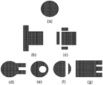
fig. 7 illustrates (a) a conventional reticle feature used to form a support post, according to an embodiment of the invention; and (b) to (g) several alternative proposals for modified reticle features that introduce focus dependency;
FIG. 8 is a schematic view of the vertically integrated memory device of FIG. 6 illustrating another embodiment of the invention.
Detailed Description
In this document, the terms "radiation" and "beam" are used to encompass all types of electromagnetic radiation, including ultraviolet radiation (e.g. having a wavelength of 365nm, 248nm, 193nm, 157nm or 126nm) and EUV (extreme ultraviolet radiation, e.g. having a wavelength in the range of about 5nm to 100 nm).
The terms "reticle", "mask" or "patterning device" used herein should be broadly interpreted as referring to a generic patterning device that can be used to impart an incident radiation beam with a patterned cross-section corresponding to a pattern to be created in a target portion of the substrate. In this case, the term "light valve" may also be used. Examples of other such patterning devices, in addition to classical masks (transmissive or reflective, binary, phase-shifting, hybrid, etc.), include programmable mirror arrays and programmable LCD arrays.
FIG. 1 schematically depicts a lithographic apparatus LA. The lithographic apparatus LA includes an illumination system (also referred to as an illuminator) IL configured to condition a radiation beam B (e.g. UV radiation, DUV radiation or EUV radiation); a mask support (e.g. a mask table) MT constructed to support a patterning device (e.g. a mask) MA and connected to a first positioner PM configured to accurately position the patterning device MA in accordance with certain parameters; a substrate support (e.g. a wafer table) WT constructed to hold a substrate (e.g. a resist-coated wafer) and connected to a second positioner PW configured to accurately position the substrate support in accordance with certain parameters; and a projection system PS (e.g. a refractive projection lens system) configured to project a pattern imparted to the radiation beam B by patterning device MA onto a target portion C (e.g. comprising one or more dies) of the substrate W.
In operation, the illumination system IL receives a radiation beam from a radiation source SO, e.g., via a beam delivery system BD. The illumination system IL may include various types of optical components, such as refractive, reflective, magnetic, electromagnetic, electrostatic and/or other types of optical components, or any combination thereof, for directing, shaping, and/or controlling radiation. The illuminator IL may be used to condition the radiation beam B to have a desired spatial intensity distribution and angular intensity distribution in cross-section at the plane of the patterning device MA.
The term "projection system" PS as used herein should be broadly interpreted as encompassing any type of projection system, including refractive, reflective, catadioptric, anamorphic, magnetic, electromagnetic and/or electrostatic optical systems, or any combination thereof, depending on the exposure radiation being used, and/or other factors such as the use of an immersion liquid or the use of a vacuum. Any use of the term "projection lens" herein may be considered as synonymous with the more general term "projection system" PS.
The lithographic apparatus LA may be of the following type: wherein at least a portion of the substrate may be covered by a liquid having a relatively high refractive index (e.g. water) so as to fill a space between the projection system PS and the substrate W, also referred to as immersion lithography. More information on immersion technology is given in US6952253, which is incorporated herein by reference.
The lithographic apparatus LA may also be of a type having two or more substrate supports WT (also referred to as a "dual stage"). In such "multiple stage" machines the substrate supports WT may be used in parallel, and/or steps in preparation for subsequent exposure of the substrate W may be carried out on a substrate W positioned on one of the substrate supports WT while another substrate W on another substrate support WT is being used to expose a pattern on another substrate W.
In addition to the substrate support WT, the lithographic apparatus LA may include a measurement table. The measuring table is arranged to hold the sensor and/or the cleaning device. The sensor may be arranged to measure a property of the projection system PS or a property of the radiation beam B. The measurement station may hold a plurality of sensors. The cleaning apparatus may be arranged to clean a part of the lithographic apparatus, for example a part of the projection system PS or a part of the system providing the immersion liquid. The measurement table may be moved under the projection system PS while the substrate support WT is away from the projection system PS.
In operation, the radiation beam B is incident on the patterning device, e.g., the mask MA, which is held on the mask support MT and is patterned by the pattern (design layout) present on the patterning device MA. After passing through the mask MA, the radiation beam B passes through the projection system PS, which focuses the beam onto a target portion C of the substrate W. With the aid of the second positioner PW and position measurement system IF, the substrate support WT can be moved accurately, e.g. so as to position different target portions C in the path of the radiation beam B in focus and alignment. Likewise, the first positioner PM and possibly another position sensor (which is not explicitly depicted in fig. 1) can be used to accurately position the patterning device MA with respect to the path of the radiation beam B. Patterning device MA and substrate W may be aligned using mask alignment marks M1, M2 and substrate alignment marks P1, P2. Although the substrate alignment marks P1, P2 as illustrated occupy dedicated target portions, they may be located in spaces between target portions. When substrate alignment marks P1, P2 are located between target portions C, they are referred to as scribe-lane alignment marks.
As shown in fig. 2, the lithographic apparatus LA may form part of a lithographic cell LC, sometimes also referred to as a lithographic cell or (lithographic) cluster, which typically also includes means for performing pre-exposure and post-exposure processes on the substrate W. Traditionally, these include spin coaters SC, which are used to deposit resist layers; a developer DE for developing the exposed resist; a cooling plate CH; and a bake plate BK, for example, for adjusting the temperature of the substrate W, for example, for adjusting a solvent in the resist layer. The substrate handler or robot RO picks up the substrate W from the input/output ports I/O1, I/O2, moves the substrate W between different processing devices, and delivers the substrate W to the feed table LB of the lithographic apparatus LA. The equipment in the lithographic unit, which are also commonly referred to as tracks, are typically controlled by a track control unit TCU, which may itself be controlled by a supervisory control system SCS, which may also control the lithographic device LA, e.g. via a lithographic control unit LACU.
In order for a substrate W exposed by the lithographic apparatus LA to be correctly and consistently exposed, it is desirable to inspect the substrate to measure properties of the patterned structure, such as overlay error between subsequent layers, line width, Critical Dimension (CD), etc. To this end, an inspection tool (not shown) may be included in the lithography unit LC. If an error is detected, adjustments may be made, for example, to the exposure of subsequent substrates or other processing steps to be performed on the substrates W, especially if the inspection is completed before other substrates W of the same lot or stack are still to be exposed or processed.
The inspection device, which may also be referred to as a metrology device, is used to determine properties of the substrate W, in particular how the properties of different substrates W vary or how properties associated with different layers of the same substrate W vary from layer to layer. Alternatively, the inspection device may be configured to identify defects on the substrate W, and may for example be part of the lithography unit LC, or may be integrated into the lithography device LA, or may even be a stand-alone apparatus. The inspection device may measure properties on the latent image (image in the resist layer after exposure), the semi-latent image (image in the resist layer after the post-exposure bake step PEB) or the developed resist image (where either the exposed or unexposed portions of the resist have been removed) or even the etched image (after a pattern transfer step such as etching).
Generally, the patterning process in the lithographic apparatus LA is one of the most critical steps in the process, which requires a high accuracy of the dimensioning and placement of the structures on the substrate W. To ensure such high accuracy, the three systems may be combined into a so-called "global" control environment, as schematically depicted in fig. 3. One of these systems is a lithographic apparatus LA, which is (virtually) connected to a metrology tool MT (second system) and a computer system CL (third system). The key to this "global" environment is to optimize the cooperation between the three systems to enhance the overall process window and to provide a tight control loop to ensure that the patterning performed by the lithographic apparatus LA remains within the process window. The process window defines a range of process parameters (e.g. dose, focus, overlap) within which a particular manufacturing process produces a defined result (e.g. a functional semiconductor device), i.e. typically within which process parameters in a lithographic process or a patterning process are allowed to vary.
The computer system CL may use (a part of) the design layout to be patterned to predict which resolution enhancement techniques to use and perform computational lithography simulations and calculations to determine which mask layouts and lithographic device settings implement the maximum overall process window of the patterning process (depicted in fig. 3 by the double arrow in the first scale SC 1). Typically, resolution enhancement techniques are arranged to match the patterning possibilities of the lithographic apparatus LA. The computer system CL may also be used to detect where within the process window the lithographic device LA is currently operating (e.g. using input from the metrology tool MT) to predict whether a defect (depicted in fig. 3 by the arrow pointing to "0" in the second scale SC 2) may be present due to, for example, sub-optimal processing.
The metrology tool MT may provide input to the computer system CL to enable accurate simulation and prediction, and may provide feedback to the lithographic apparatus LA to identify possible drift, for example, in a calibration state of the lithographic apparatus LA (depicted in fig. 3 by the plurality of arrows in the third scale SC 3).
In a lithographic process, it is desirable to make frequent measurements of the resulting structure, for example, for process control and verification. Various tools for making such measurements are known, including scanning electron microscopes or various forms of metrology devices such as scatterometers. Examples of known scatterometers typically rely on providing a dedicated metrology target, such as an under-filled target (a target in the form of a simple grating or overlapping gratings in different layers of sufficient size that the measurement beam generates a spot smaller than the grating) or an over-filled target (whereby the illumination spot partially or completely encompasses the target). Further, the use of metrology tools (e.g. angle-resolved scatterometers such as gratings illuminating under-filled targets) allows the use of so-called reconstruction methods, where the properties of the gratings can be calculated by simulating the interaction of the scattered radiation with a mathematical model of the target structure and comparing the simulation results with the measurement results. The parameters of the model are adjusted until the simulated interaction produces a diffraction pattern similar to the diffraction pattern observed from the actual target.
Scatterometers are general purpose instruments that allow measuring parameters of the lithographic process by having a sensor in the pupil or in a plane conjugate to the pupil of the objective of the scatterometer, the measurement is usually called pupil based measurement, or by having a sensor in the image plane or in a plane conjugate to the image plane, in which case the measurement is usually called image based or field based measurement. Such scatterometers and associated measurement techniques are further described in U.S. patent applications US20100328655, US2011102753a1, US20120044470A, US20110249244, US20110026032 or ep1,628,164a, the entire contents of which are incorporated herein by reference. The aforementioned scatterometer can measure multiple targets from multiple gratings in one image using light from soft X-rays and the visible to near infrared range.
A metrology device, such as a scatterometer, is depicted in fig. 4. The metrology apparatus comprises a broadband (white light) radiation projector 2 which projects radiation 5 onto a substrate W. The reflected or scattered radiation 10 is passed to a spectrometer detector 4 which measures the spectrum 6 (i.e. the intensity I is measured as a function of the wavelength λ) of the specularly reflected radiation 10. From this data, the structure or profile 8 that produced the detected spectrum can be reconstructed by the processing unit PU, for example by rigorous coupled wave analysis and non-linear regression or by comparison with a library of simulated spectra. In general, for reconstruction, the general form of the structure is known and some parameters are assumed from knowledge of the process of manufacturing the structure, so that only a few parameters of the structure are determined from the scatter data. Such a scatterometer may be configured as a normal incidence scatterometer or an oblique incidence scatterometer.
FIG. 5(a) shows an alternative metrology device suitable for use in embodiments of the present invention. The target T and the diffracted rays of the measuring radiation used to illuminate the target are illustrated in more detail in fig. 5 (b). The illustrated metrology apparatus is of the type known as a dark field metrology apparatus. The metrology device may be a standalone apparatus, or may be incorporated into the lithographic apparatus LA (e.g. at a metrology station), or into the lithographic cell LC. The optical axis with several branches in the whole device is indicated by the dashed line O. In this apparatus, light emitted from a light source 11 (for example, a xenon lamp) is guided onto a substrate W via a beam splitter 15 by an optical system including lenses 12, 14 and an objective lens 16. These lenses are arranged in a double order of 4F arrangement. A different lens arrangement may be used as long as it still provides a substrate image onto the detector while allowing access to intermediate pupil planes for spatial frequency filtering. Thus, the range of angles at which radiation is incident on the substrate can be selected by defining a spatial intensity distribution in a plane (referred to herein as the (conjugate) pupil plane) that exhibits the spatial spectrum of the substrate plane. This may be done, in particular, by inserting an aperture plate 13 of suitable form between the lenses 12 and 14 in a plane which is the inverse of the image projected in the pupil plane of the objective lens. In the illustrated example, the aperture plate 13 has different forms, labeled 13N and 13S, allowing different illumination modes to be selected. The illumination system in this example forms an off-axis illumination mode. In the first illumination mode, the aperture plate 13N provides (for descriptive purposes only) an off-axis offset from the direction designated as 'north'. In the second illumination mode, the aperture plate 13S is used to provide similar illumination, but from the opposite direction, labeled 'south'. Other illumination modes are possible by using different apertures. The rest of the pupil plane is desired to be dark, since any unnecessary light outside the desired illumination mode will interfere with the desired measurement signal.
As shown in fig. 5(b), the target T is placed together with the substrate W so as to be orthogonal to the optical axis O of the objective lens 16. The substrate W may be supported by a support (not shown). The measurement radiation ray I incident on the target T from an angle off the axis O generates a zero-order ray (solid line 0) and two first-order rays (dot chain line +1 and two dot chain line-1). It should be kept in mind that in the case of an overfilled small target, these rays are only one of many parallel rays that cover the area of the substrate including the metrology target T and other features. Since the holes in the plate 13 have a limited width (a useful amount of light must be admitted), in practice the incident radiation I will occupy a range of angles and the diffracted radiation 0 and +1/-1 will be slightly spread out. According to the point spread function of a small target, each order of +1 and-1 is further spread over a range of angles, rather than a single ideal ray as shown. It should be noted that the grating pitch and illumination angle of the target may be designed or adjusted to closely align the first order rays entering the objective lens with the central optical axis. The rays illustrated in fig. 5(a) and 3(b) are shown slightly off-axis, purely to make them easier to distinguish in the figure.
At least the 0 and +1 orders diffracted by the target T on the substrate W are collected by the objective lens 16 and directed back through the beam splitter 15. Returning to fig. 5(a), the first and second illumination modes are illustrated by designating diametrically opposed apertures labeled north (N) and south (S). When the incident ray I of the measurement radiation comes from the north side of the optical axis, that is, when the first irradiation mode is applied using the aperture plate 13N, the +1 diffracted ray labeled +1(N) enters the objective lens. Except that, when the second illumination mode is applied using the aperture plate 13S, the-1 diffracted radiation (labeled 1(S)) is the radiation that enters the lens 16.
The second beam splitter 17 splits the diffracted beam into two measurement branches. In the first measurement branch, the optical system 18 forms a diffraction spectrum (pupil plane image) of the target on a first sensor 19 (e.g., a CCD sensor or a CMOS sensor) using the zero-order diffracted beam and the first-order diffracted beam. Each diffraction order hits a different point on the sensor so that the image processing can compare and contrast the orders. The pupil plane image captured by the sensor 19 may be used to focus the metrology device and/or to normalize the intensity measurements of the first order beam. The pupil plane image may also be used for many measurement purposes, such as reconstruction.
In the second measurement branch, the optical system 20, 22 forms an image of the target T on a sensor 23 (e.g. a CCD sensor or a CMOS sensor). In the second measurement branch, an aperture stop 21 is provided in a plane conjugate to the pupil plane. The aperture stop 21 functions to block the zero order diffracted beam so that the image of the target formed on the sensor 23 is formed of only the-1 order beam or the +1 order beam. The images captured by the sensors 19 and 23 are output to a processor PU which processes the images, the function of which will depend on the particular type of measurement being performed. It should be noted that the term 'image' is used broadly herein. If there is only one of the-1 order and the +1 order, an image of such a raster line will not be formed.
The particular form of the aperture plate 13 and field stop 21 shown in fig. 5 is merely exemplary. In another embodiment of the invention, on-axis illumination of the target is used, and an aperture stop with an off-axis aperture is used to pass substantially only one first order diffracted light to the sensor. In yet other embodiments, a second order beam, a third order beam, and higher order beams (not shown in FIG. 5) may be used in the measurement instead of or in addition to the first order beam.
To adapt the measurement radiation to these different types of measurements, the aperture plate 13 may include a plurality of aperture patterns formed around a disk that rotates to place the desired pattern in place. It should be noted that the aperture plate 13N or 13S can only be used to measure gratings oriented in one direction (X or Y depending on the setting). For measuring orthogonal gratings, target rotation through 90 ° and 270 ° may be achieved. Fig. 3(c) and 3(d) show different orifice plates. The use of these orifice plates, as well as many other variations and applications of the device, are described in the previously disclosed applications mentioned above.
When monitoring a lithographic process, it is desirable to monitor a lithographic process parameter, such as the focus of the lithographic beam on the substrate. One known method of determining focus settings from printed structures is by measuring the Critical Dimension (CD) of the printed structure. CD is a measure of the smallest feature (e.g., line width of a component). The printed structure may be a target formed specifically for focus monitoring, such as a line-space grating. As is well known, CDs will typically exhibit a second order response to focus, forming a so-called "Bossung curve" on a plot of CD (y-axis) versus focus (x-axis). The Bossung curve is a substantially symmetric curve that is substantially symmetric around the peak representing best focus. The shape of the Bossung curve may be substantially parabolic. This approach has several disadvantages. One disadvantage is that this method shows a lower sensitivity (due to the parabolic shape of the curve) near the best focus. Another disadvantage is that the method is insensitive to any sign of defocus (because the curve is substantially symmetric around best focus). Furthermore, the method is particularly sensitive to dose and process variations (cross-talk).
To solve these problems, diffraction-based focusing (DBF) was devised. Diffraction-based focusing can use target-forming features on a reticle that print targets with a degree of asymmetry that depends on the focus setting during printing. This degree of asymmetry can then be measured using a scatter-based inspection method (e.g., by measuring the intensity asymmetry between the intensities of +1 and-1 order radiation diffracted from the target) to obtain a measurement of the focus setting.
To fabricate vertically integrated devices (e.g., memory devices), such as vertical NAND or 3D NAND, very thick (tall) multi-layer stacks are fabricated onto a substrate. A deep etch process is then performed to form contact holes through the stack. The height of these multilayer stacks may for example be larger than 10 μm in a direction perpendicular to the substrate surface. During deposition of these layers, non-uniformities in the deposition rate and tension of the applied layers can create a topological profile on the stack surface that can negatively impact lithography of subsequent layers.
For this reason, focus control in forming some layers is very important for such devices. In particular, the layers defining the contact holes to be etched through the entire multilayer structure are particularly sensitive to focusing. To control focus during the manufacture of these devices, feedback correction methods may be employed based on measurements of structures performed on previously processed substrates. From these measurements, the focus setting used to form the measurement structure can be deduced. For example, currently, one or more of the following methods may be used to determine focus:
direct measurements are made on production wafers using diffraction-based focus (DBF) techniques based on measurements of metrology targets formed in scribe lines. By being designed with focus-based asymmetry, DBF technology uses a focus target with a unique metrology function/purpose. By measuring the asymmetry of the target (e.g., by using a scatterometer), the focus setting used in its formation can be determined. These techniques may also be referred to as micro-DBF (μ DBF), especially if dark field techniques are used to measure smaller objects. Such techniques are described in the following documents: US9182682B2, US9081303B2, US8994944B 2; and similar techniques are described in the following documents: US9594299B2, US20160313656a1, US20160363871a 1. All of these documents are incorporated herein by reference.
Focus is measured via CDSEM (critical dimension scanning electron microscope) technology based on the measurement of a specific mark deposited on top of the device (again with a unique metrology function/purpose).
Indirect focus measurements via computational metrology techniques or other methods that computationally model focus settings.
Measurements based on structures in scribe lines often suffer from variable measurement offsets between scribe line structures and device structures (e.g., different relationships between focus and its effect on the formed structures). This may make the inferred focus value less reliable (e.g., a focus value that does not truly represent a device feature), and thus any correction based on these measurements may be compromised. However, performing measurements directly on structures in the facility area (i.e., using CDSEM) requires the formation of specific target structures that are generally incompatible with the product, and requires reticles that are different from the reticles used to form the product structures. This means that the substrate must then be reworked to remove the layer comprising the focus marks. Additionally, CDSEM examination is very slow.
Therefore, it is proposed to develop a method that enables DBF (or μ DBF) technology to be applied to a device area of a vertical integrated circuit (e.g., 3D NAND). Such a method may enable focus measurements to be performed in the region of the device using a scatterometer (e.g. using a metrology device as shown in figure 4 or figure 5 (a)).
More specifically, it is proposed to form a modified substrate feature of an apparatus, the modified substrate feature being formed for a primary function other than metrology, the modification being such that the modified substrate feature has a secondary metrology function, more specifically still for measurement focus. In one embodiment, the modified substrate feature may have no electrical function within the working device. This particular implementation based on the modification of the support features is described below. However, in alternative embodiments, some features having some electrical functions (such as features defining large contact pads or interconnects) may also be suitable for modification for secondary metrology purposes within the scope of the present disclosure.
The modification may be effected via a modified reticle feature so as to introduce a measurable feature focus correlation. In one embodiment, in a similar manner to DBF, the focus correlation may include a focus-related asymmetry in the feature (e.g., a Side Wall Angle (SWA) asymmetry). After the photoresist layer is developed, the feature may be a hole in the photoresist layer, and at one or more particular sides of the hole, the walls of the photoresist facing the interior of the hole may have a focus-related asymmetry, e.g., a focus-related Side Wall Angle (SWA). This may be achieved by providing the modified reticle features with one or more specific assist features (e.g., sub-resolution sub-features) that impose a focus-related geometry (asymmetry) on the exposed features.
In one principal embodiment, the modified substrate features may be associated with the formation of support structures or support posts for supporting vertical integrated circuit devices. As such, it is proposed to form a focus target on the features used to form the support posts; wherein the focus target comprises a target having a focus correlation, more particularly a focus-related asymmetry, that can be measured to determine or infer a focus value for use during formation of the target.
In order to support the vertically integrated structures so that they remain stable when the nitride layer of the stack is etched away prior to the tungsten fill step, support structures or support posts are typically provided. These support posts are formed in the same way as the array of cells, i.e. by exposing support or aperture features onto the substrate from a corresponding pattern on the reticle. These support features are then filled in subsequent processing steps (e.g., etching) to provide structural support posts. Since these posts do not have any electrical function, there is (limited) freedom to modify their shape without affecting the performance of the device. More specifically, there is (limited) freedom to modify the 3d dimensional shape of the holes in the layer of photoresist material.
FIG. 6 shows (a) oblique projections (the directions shown are the bit line direction BL, word line direction WL, and Z direction perpendicular to these aspects); (b) a top view of a pair of vertically integrated cell arrays 600a, 600b formed on a substrate 610. The cell arrays 600a, 600b are substantially frustum-shaped with each side having a stepped profile (stepped structure). A top-down detail 620 of the top of one cell array 600b is shown. The cell array can be viewed as comprising rows of memory holes 630 (larger circular structures) and rows of features (holes) for support posts 640 (smaller circular structures). What can be modified according to embodiments is a support post feature.
Fig. 7(a) shows a typical pattern (reticle feature) for defining these post features, which comprises simple circles. However, this is a simplified diagram; more practically, the reticle pattern may comprise one or more Optical Proximity Correction (OPC) assist features. In this case, however, it should be appreciated that such OPC features are presently included in order to form circular features on the substrate as symmetrically as possible (regardless of focus).
Fig. 7(b) -7 (f) illustrate several possible modifications (modified reticle features) of the pattern of fig. 7(a) which, after development, introduce the desired focus-related asymmetry, e.g. in the resulting structure in a photoresist layer (modified substrate structure). These modified substrate structures can be measured using a scatterometer (or other metrology device) to produce an asymmetric signal proportional to focus in a manner similar to DBF/μ DBF.
Fig. 7(b) and 7(c) show OPC (assist feature) embodiments that may be applied. The basic idea is that the exposed shape (geometry or profile) of the pillar feature should have a different dimension (e.g., radius) over the first portion of the pillar cross-section, as viewed from above (e.g., about the first half), compared to the diameter of the second portion of the pillar cross-section (e.g., about the second half). The resulting pillars have a substantially elliptical shape (egg shape), with asymmetry depending on focus. Fig. 7(b) and 7(c) show possible alternative reticle features for producing such posts, or although it will be appreciated that these are purely examples and other feature shapes are possible which achieve roughly the same effect.
Fig. 7(d) -7 (g) show other possible reticle features that may also achieve the desired focus-related asymmetry while still etching approximately circular posts suitable for the support structure.
In one embodiment, the pattern for at least some of the support columns on the reticle may be replaced by an arrangement of focus targets (e.g., appropriately divided according to design rules so that each segment is sufficiently similar to the scheme of support columns). After forming them and measuring them, a deep etching step is performed during which the focus targets are etched through the multilayer structure and filled in a similar manner to the support posts. In this way, the focus target acts as a support post and becomes part of the structure after deep etching.
One or more patterns (modified reticle features) according to the patterns of fig. 7(b) -7 (g) may be provided on a patterning device that may be used in a lithographic apparatus to print or form one or more modified substrate features on a substrate (e.g. in a photoresist layer). In the context of the present invention, the terms "reticle", "mask" have the same meaning as the term patterning device.
In an alternative embodiment, it is proposed to incorporate the focus target on a staircase structure of the cell array. Fig. 8 illustrates such an example, and fig. 8 includes a top view of the vertical integrated structure at the top of fig. 6. A stair-step structure is a well-known feature of vertical integrated circuits to enable connection to each layer in a stack. In practice, the stair-step structure 820a on only two sides of each cell array 800a, 800b is actually used for electrical connection. Nonetheless, due to the manufacturing process, the stair-step structure 820b is also formed on two other sides, each side having the same size and profile as the stair-step structure 820a, but not for electrical connection. It is proposed to place focus related targets on these unused stair structures 820 b.
A typical μ DBF target may comprise four segments, each segment forming a quadrant of the complete target. The four segments may include two focus sensitive segments (one segment for each direction) and two corresponding dose sensitive segments. The dose value inferred from the dose sensitive segment can be used to calibrate the focus measurement from the focus sensitive segment. Such objects are for example described in WO2013/189724, which is incorporated herein by reference. However, due to the size of the stepped structure (which may be only 5 μm in the narrower dimension), such targets cannot be accommodated thereon. Thus, for this embodiment, a modified focus (μ DBF) target 830 is proposed, which may be integrated on the unused (sacrificial) step area 820b of the cell array. The modified μ DBF target 830 comprises two focus sensitive segments 830a, 830b (one focus sensitive segment in each direction) and two dose sensitive segments 830c, 830D (one dose sensitive segment in each direction), all arranged in the same line (row), i.e. in a 1D array. Thus, the narrowest dimension of such a target may be set to 10 μm or less, or even 5 μm or less. Several of these targets 830 may be accommodated in one or both of the unused step areas 820 b.
The above method is described only in terms of determining the focus setting (actual focus) of the lithographic apparatus used. However, it will be appreciated that the method may also be used to determine one or more other characteristics relating to one or more structures on the substrate, for example, the dose setting (actual dose) used.
The method described above describes a modification of the features (more specifically, the support features) formed without electrical function. However, the concepts herein are also applicable to features that do have some electrical function, such as large contact pads or interconnects. As such, modifications to these features for secondary metrology purposes are also within the scope of the present disclosure.
This proposal described herein provides accurate focus measurements directly on the device area, improving any other measurement method that uses targets in other field positions. This means that the target pattern may be included on the product reticle and printed on the product substrate as part of the actual manufacturing process. In this way, the focus from the actual product substrate can be measured from the printed structure formed by the same illumination and during the same exposure as the product structure. The proposal also provides a measurement method that requires a CDSEM and rework of the wafer because it is faster than current methods for measuring focus on the device area.
Other embodiments are disclosed in the subsequent numbered clauses:
1. a method of determining a characteristic of interest relating to a structure on a substrate, the structure being formed by a lithographic process, the method comprising:
measuring a modified substrate feature to determine the characteristic of interest, wherein the modified substrate feature is formed on a substrate using a corresponding modified reticle feature on a patterning device, the modified substrate feature being formed for a primary function other than metrology, the modified reticle feature being such that the modified substrate feature is formed with a geometry that depends on the characteristic of interest during formation.
2. The method of clause 1, further comprising the step of forming the modified substrate feature on a substrate using the corresponding modified reticle feature on the patterning device.
3. The method of clause 1 or 2, wherein the modified substrate feature has no electrical function.
4. The method of any of the preceding clauses wherein the characteristic of interest is focus of a lithographic device during formation of the modified substrate feature.
5. The method of clause 4, wherein the geometry that depends on the characteristic of interest includes a focus-related asymmetry, which can be measured in the measuring step.
6. The method of clause 4 or 5, wherein the lithographic process is related to the formation of a vertically integrated structure, and the modified substrate feature has a primary function related to the support of the vertically integrated structure.
7. The method of clause 6, wherein the modified substrate features comprise support features for forming support structures for the vertically integrated structures.
8. The method of clause 7, wherein the support feature comprises a hole feature.
9. The method of clause 7 or 8, comprising: after the forming and measuring steps, filling the support features when aligned with corresponding support features in other layers to form the support structure.
10. The method of any of clauses 6-9, wherein the vertically integrated structure comprises a stair-step structure at its periphery and the modified substrate feature is formed on a region of the substrate corresponding to the stair-step structure.
11. The method of clause 10, wherein the modified substrate feature is formed on a region of the substrate region corresponding to the stair-step structure on a side of the vertically integrated structure where no electrical connection to the stair-step structure is formed.
12. The method of any of clauses 3-11, wherein the modified reticle feature is such that a dimension of a first portion of the corresponding modified substrate feature differs from a dimension of a second portion of the corresponding modified substrate feature in a focus-related manner.
13. The method of any of clauses 3-12, wherein the modified reticle features are such that they induce a focus-related elliptical geometry in the corresponding modified substrate features.
14. The method of any preceding clause, wherein the modified reticle feature has been designed using an optical proximity correction technique.
15. The method of any preceding clause, wherein the measuring step is performed using a scatterometer.
16. The method of any of the preceding clauses wherein the measuring step comprises: measuring an asymmetry in the modified substrate feature; and determining the characteristic of interest from the modified substrate feature.
17. The method of any of the preceding clauses wherein the step of forming the modified substrate feature is performed concurrently with the formation of the contact hole layer.
18. The method of any of the preceding clauses wherein the modified substrate features are formed on a device region of the substrate that includes a product structure.
19. The method of any of the preceding clauses wherein the characteristic of interest comprises a dose of a lithographic device during formation of the modified substrate feature.
20. A patterning device comprising a modified reticle feature for forming a modified substrate feature on a substrate, the geometry of the modified substrate feature being dependent on a property of interest during its formation, and wherein the modified substrate feature has a primary function other than metrology.
21. The patterning device of clause 20, wherein the modified substrate feature is electrically non-functional.
22. The patterning device of clause 20 or 21, wherein the characteristic of interest is focus during formation of the modified substrate feature.
23. The patterning device of clause 22, wherein the geometry that depends on the property of interest comprises a focus-related asymmetry.
24. The patterning device of clause 22 or 23, wherein the patterning device is used to pattern a layer of a vertically integrated structure and the modified substrate features have a primary function related to the support of the vertically integrated structure.
25. The patterning device of clause 24, wherein the modified substrate features comprise features for forming support structures for the vertically integrated structures.
26. The patterning device of clause 25, wherein the support features comprise hole features.
27. The patterning device of clause 24, 25 or 26, wherein the vertically integrated structure comprises a stair step structure at its periphery and the modified reticle feature is located on a region of the patterning device corresponding to the stair step structure.
28. The patterning device of clause 27, wherein the modified reticle feature is located on a region of the patterning device corresponding to the stair step structure on a side of the vertically integrated structure that does not form an electrical connection to a stair step structure.
29. The patterning device of any of clauses 22 to 28, wherein the modified reticle feature is such that a dimension of a first portion of the corresponding modified substrate feature differs from a dimension of a second portion of the corresponding modified substrate feature in a focus-related manner.
30. The patterning device of any of clauses 22 to 29, wherein the modified reticle features are such that they cause focus-related elliptical geometries in the corresponding modified substrate features.
31. The patterning device of any of clauses 20 to 30, wherein the modified reticle feature has been designed using an optical proximity correction technique.
32. The patterning device of any of clauses 20 to 31, wherein the measuring step is performed using a scatterometer.
33. The patterning device of any of clauses 20 to 32, wherein the measuring step comprises: measuring an asymmetry in the modified substrate feature; and determining the characteristic of interest from the modified substrate feature.
34. The patterning device of any of clauses 20 to 33, wherein the patterning device further comprises features for forming contact holes.
35. The patterning device of any of clauses 20 to 34, wherein the modified reticle feature is located on a tool area of the patterning device.
36. A lithography system for determining a characteristic of interest relating to at least one structure on a substrate, the at least one structure being formed by a lithographic process, the lithography system comprising:
patterning means as defined in any of clauses 20 to 35 for forming subsequent modified substrate features on the substrate; and
metrology apparatus for performing the measurement steps according to any of clauses 1 to 19.
37. A non-transitory computer program product comprising machine readable instructions for causing a processor to cause performance of the method according to any one of clauses 1 to 19.
38. A method of determining a focus setting associated with forming a structure on a substrate by a lithographic process during fabrication of a vertical integrated structure, the method comprising:
forming substrate support features on the substrate using corresponding reticle support features for providing a support structure for the vertically integrated structure, the reticle support members being such that the substrate support features are formed with a geometry that depends on a property of interest during formation thereof; and
measuring the substrate support feature to determine the focus setting.
39. A patterning device for patterning a layer of a vertically integrated structure, comprising a reticle support feature for forming a substrate support feature on a substrate, the geometry of the substrate support feature being dependent on a focus setting during its formation, and wherein the substrate support feature is for providing a support structure for the vertically integrated structure.
Although specific reference may be made in this text to the use of lithographic apparatus in the manufacture of ICs, it should be understood that the lithographic apparatus described herein may have other applications. Other possible applications include the manufacture of integrated optical systems, guidance and detection patterns for magnetic domain memories, flat panel displays, Liquid Crystal Displays (LCDs), thin film magnetic heads, etc.
Although embodiments of the present invention may be specifically referenced herein in the context of an inspection device or a metrology device, embodiments of the present invention may be used with other devices. Embodiments of the invention may form part of a mask inspection device, a lithographic apparatus, or any device that measures or processes an object such as a wafer (or other substrate) or a mask (or other patterning device). It should also be noted that the term measurement device or measurement system encompasses the term inspection device or inspection system or may be used instead. The metrology or inspection apparatus disclosed herein may be used to detect defects on or within a substrate and/or defects of structures on a substrate. In such embodiments, for example, the characteristic of a structure on the substrate may be related to a defect in the structure, the absence of a particular portion of the structure, or the presence of an unwanted structure on the substrate.
While specific embodiments of the invention have been described above, it will be appreciated that the invention may be practiced otherwise than as described. The above description is intended to be illustrative, and not restrictive. Thus, it will be apparent to one skilled in the art that modifications may be made to the invention as described without departing from the scope of the claims set out below.
Claims (15)
1. A method of determining a characteristic of interest relating to a structure on a substrate, the structure being formed by a lithographic process, the method comprising:
measuring a modified substrate feature to determine the characteristic of interest, wherein the modified substrate feature is formed on the substrate using a corresponding modified reticle feature on a patterning device, the modified substrate feature being formed for a primary function other than metrology, the modified reticle feature being such that the modified substrate feature is formed with a geometry that depends on the characteristic of interest during formation thereof.
2. The method of claim 1, further comprising the stage of forming the modified substrate features on the substrate using the corresponding modified reticle features on the patterning device.
3. The method of claim 1 or 2, wherein the modified substrate feature has no electrical function.
4. The method of any preceding claim, wherein the characteristic of interest is focus of a lithographic apparatus during formation of the modified substrate feature, and optionally the geometry dependent on the characteristic of interest comprises a focus-dependent asymmetry, which can be measured in the measuring step.
5. The method of claim 3 or 4, wherein the lithographic process is associated with the forming of a vertically integrated structure and the modified substrate feature has a primary function associated with support of the vertically integrated structure.
6. The method of claim 5, wherein the modified substrate features comprise support features for forming support structures for the vertically integrated structures.
7. The method of claim 6, wherein the support features comprise hole features.
8. The method of any of claims 5 to 7, wherein the vertically integrated structure comprises a stair-step structure at its periphery and the modified substrate feature is formed on a region of the substrate corresponding to the stair-step structure, and wherein optionally the modified substrate feature is formed on a region of the substrate region corresponding to the stair-step structure on a side of the vertically integrated structure not forming an electrical connection with the stair-step structure.
9. The method of claim 8, wherein the modified substrate features are formed on regions of the substrate region corresponding to the stair-step structures on a side of a vertically integrated structure that does not form an electrical connection with the stair-step structures.
10. The method of any of claims 2 to 9, wherein the modified reticle feature is such that a dimension of a first portion of the corresponding modified substrate feature differs from a dimension of a second portion of the corresponding modified substrate feature in a focus-related manner.
11. The method of any of claims 3 to 10, wherein the modified reticle features are such that they induce focus-related elliptical geometries in the corresponding modified substrate features.
12. The method of any of the preceding claims, wherein the step of forming modified substrate features is performed simultaneously with the formation of a contact hole layer.
13. A patterning device comprising a modified reticle feature for forming a modified substrate feature on a substrate, the geometry of the modified substrate feature being dependent on the characteristic of interest during its formation, and wherein the modified substrate feature has a primary function other than metrology.
14. A lithography system for determining a characteristic of interest relating to at least one structure on a substrate, the at least one structure being formed by a lithographic process, the lithography system comprising:
the patterning device of claim 13, for forming subsequent modified substrate features on a substrate; and
metrology apparatus for performing the measurement steps according to any one of claims 1 to 12.
15. A non-transitory computer program product comprising machine readable instructions for causing a processor to perform the method of any of claims 1 to 12.
Priority Applications (1)
| Application Number | Priority Date | Filing Date | Title |
|---|---|---|---|
| CN202311521912.9A CN117518733A (en) | 2018-07-18 | 2019-06-19 | Metrology apparatus and method for determining characteristics related to one or more structures on a substrate |
Applications Claiming Priority (3)
| Application Number | Priority Date | Filing Date | Title |
|---|---|---|---|
| EP18184163.6A EP3598235A1 (en) | 2018-07-18 | 2018-07-18 | Metrology apparatus and method for determining a characteristic relating to one or more structures on a substrate |
| EP18184163.6 | 2018-07-18 | ||
| PCT/EP2019/066147 WO2020015947A1 (en) | 2018-07-18 | 2019-06-19 | Metrology apparatus and method for determining a characteristic relating to one or more structures on a substrate |
Related Child Applications (1)
| Application Number | Title | Priority Date | Filing Date |
|---|---|---|---|
| CN202311521912.9A Division CN117518733A (en) | 2018-07-18 | 2019-06-19 | Metrology apparatus and method for determining characteristics related to one or more structures on a substrate |
Publications (1)
| Publication Number | Publication Date |
|---|---|
| CN112424695A true CN112424695A (en) | 2021-02-26 |
Family
ID=62985944
Family Applications (2)
| Application Number | Title | Priority Date | Filing Date |
|---|---|---|---|
| CN202311521912.9A Pending CN117518733A (en) | 2018-07-18 | 2019-06-19 | Metrology apparatus and method for determining characteristics related to one or more structures on a substrate |
| CN201980047739.9A Pending CN112424695A (en) | 2018-07-18 | 2019-06-19 | Metrology apparatus and method for determining a characteristic relating to one or more structures on a substrate |
Family Applications Before (1)
| Application Number | Title | Priority Date | Filing Date |
|---|---|---|---|
| CN202311521912.9A Pending CN117518733A (en) | 2018-07-18 | 2019-06-19 | Metrology apparatus and method for determining characteristics related to one or more structures on a substrate |
Country Status (5)
| Country | Link |
|---|---|
| US (1) | US11385554B2 (en) |
| EP (1) | EP3598235A1 (en) |
| CN (2) | CN117518733A (en) |
| TW (1) | TWI706233B (en) |
| WO (1) | WO2020015947A1 (en) |
Citations (2)
| Publication number | Priority date | Publication date | Assignee | Title |
|---|---|---|---|---|
| US20150340376A1 (en) * | 2014-05-20 | 2015-11-26 | Jintaek Park | Semiconductor device and method of fabricating the same |
| US20150338749A1 (en) * | 2012-06-22 | 2015-11-26 | Asml Netherlands B.V. | Method of Determining Focus, Inspection Apparatus, Patterning Device, Substrate and Device Manufacturing Method |
Family Cites Families (17)
| Publication number | Priority date | Publication date | Assignee | Title |
|---|---|---|---|---|
| US6440616B1 (en) * | 1999-09-28 | 2002-08-27 | Kabushiki Kaisha Toshiba | Mask and method for focus monitoring |
| SG135052A1 (en) | 2002-11-12 | 2007-09-28 | Asml Netherlands Bv | Lithographic apparatus and device manufacturing method |
| US7791727B2 (en) | 2004-08-16 | 2010-09-07 | Asml Netherlands B.V. | Method and apparatus for angular-resolved spectroscopic lithography characterization |
| NL1036245A1 (en) | 2007-12-17 | 2009-06-18 | Asml Netherlands Bv | Diffraction based overlay metrology tool and method or diffraction based overlay metrology. |
| NL1036734A1 (en) | 2008-04-09 | 2009-10-12 | Asml Netherlands Bv | A method of assessing a model, an inspection apparatus and a lithographic apparatus. |
| NL1036857A1 (en) | 2008-04-21 | 2009-10-22 | Asml Netherlands Bv | Inspection method and apparatus, lithographic apparatus, lithographic processing cell and device manufacturing method. |
| US8891061B2 (en) | 2008-10-06 | 2014-11-18 | Asml Netherlands B.V. | Lithographic focus and dose measurement using a 2-D target |
| US9182682B2 (en) | 2008-12-30 | 2015-11-10 | Asml Netherlands B.V. | Inspection method and apparatus, lithographic apparatus, lithographic processing cell and device manufacturing method |
| JP5545782B2 (en) | 2009-07-31 | 2014-07-09 | エーエスエムエル ネザーランズ ビー.ブイ. | Lithographic apparatus focus measurement method, scatterometer, lithography system, and lithography cell |
| NL2007176A (en) | 2010-08-18 | 2012-02-21 | Asml Netherlands Bv | Substrate for use in metrology, metrology method and device manufacturing method. |
| US10131534B2 (en) * | 2011-10-20 | 2018-11-20 | Snaptrack, Inc. | Stacked vias for vertical integration |
| US9411223B2 (en) * | 2012-09-10 | 2016-08-09 | Globalfoundries Inc. | On-product focus offset metrology for use in semiconductor chip manufacturing |
| NL2011816A (en) * | 2012-11-30 | 2014-06-04 | Asml Netherlands Bv | Method of determining dose and focus, inspection apparatus, patterning device, substrate and device manufacturing method. |
| WO2015090839A1 (en) | 2013-12-17 | 2015-06-25 | Asml Netherlands B.V. | Inspection method, lithographic apparatus, mask and substrate |
| NL2014647A (en) * | 2014-05-13 | 2016-03-31 | Asml Netherlands Bv | Substrate and Patterning Device for use in Metrology, Metrology Method and Device Manufacturing Method. |
| IL256114B2 (en) | 2015-06-12 | 2023-10-01 | Asml Netherlands Bv | Inspection apparatus, inspection method, lithographic apparatus, patterning device and manufacturing method |
| WO2017202665A1 (en) * | 2016-05-25 | 2017-11-30 | Asml Netherlands B.V. | Focus and overlay improvement by modifying a patterning device |
-
2018
- 2018-07-18 EP EP18184163.6A patent/EP3598235A1/en not_active Withdrawn
-
2019
- 2019-06-19 CN CN202311521912.9A patent/CN117518733A/en active Pending
- 2019-06-19 WO PCT/EP2019/066147 patent/WO2020015947A1/en active Application Filing
- 2019-06-19 CN CN201980047739.9A patent/CN112424695A/en active Pending
- 2019-06-28 US US16/456,878 patent/US11385554B2/en active Active
- 2019-07-10 TW TW108124272A patent/TWI706233B/en not_active IP Right Cessation
Patent Citations (2)
| Publication number | Priority date | Publication date | Assignee | Title |
|---|---|---|---|---|
| US20150338749A1 (en) * | 2012-06-22 | 2015-11-26 | Asml Netherlands B.V. | Method of Determining Focus, Inspection Apparatus, Patterning Device, Substrate and Device Manufacturing Method |
| US20150340376A1 (en) * | 2014-05-20 | 2015-11-26 | Jintaek Park | Semiconductor device and method of fabricating the same |
Also Published As
| Publication number | Publication date |
|---|---|
| CN117518733A (en) | 2024-02-06 |
| US20200026182A1 (en) | 2020-01-23 |
| WO2020015947A1 (en) | 2020-01-23 |
| US11385554B2 (en) | 2022-07-12 |
| TW202006477A (en) | 2020-02-01 |
| EP3598235A1 (en) | 2020-01-22 |
| TWI706233B (en) | 2020-10-01 |
Similar Documents
| Publication | Publication Date | Title |
|---|---|---|
| TWI645257B (en) | Inspection method, lithographic apparatus, mask and substrate | |
| CN110553602A (en) | Metric method, computer product and system | |
| US10691030B2 (en) | Measurement method, inspection apparatus, patterning device, lithographic system and device manufacturing method | |
| TWI643030B (en) | Metrology robustness based on through-wavelength similarity | |
| EP3518040A1 (en) | A measurement apparatus and a method for determining a substrate grid | |
| TWI623822B (en) | Method and computer program for inspecting a substrate | |
| US20230305407A1 (en) | Methods and patterning devices and apparatuses for measuring focus performance of a lithographic apparatus, device manufacturing method | |
| TWI752647B (en) | Method for inferring a processing parameter such as focus and associated apparatuses and manufacturing method | |
| CN110945436A (en) | Method for parameter determination and apparatus therefor | |
| TWI706233B (en) | Method, patterning device, lithographic system and non-transitory computer program product of determining a characteristic of interest relating to a structure on a substrate formed by a lithographic process | |
| US11733615B2 (en) | Methods and patterning devices and apparatuses for measuring focus performance of a lithographic apparatus, device manufacturing method | |
| US20230035073A1 (en) | Method for determining a measurement recipe and associated apparatuses | |
| EP4155821A1 (en) | Method for focus metrology and associated apparatuses | |
| TWI836599B (en) | Method of determining a metrology contribution from statistically independent sources, method of determining a parameter of interest of a lithographic process, and related computer program and non-transient computer program carrier | |
| US11372343B2 (en) | Alignment method and associated metrology device | |
| EP4160314A1 (en) | Method for measuring at least one target on a substrate | |
| EP3796088A1 (en) | Method and apparatus for lithographic process performance determination | |
| CN117940852A (en) | Method for focus metrology and associated apparatus | |
| EP3786711A1 (en) | Non-correctable error in metrology | |
| EP3650941A1 (en) | Method of determining the contribution of a processing apparatus to a substrate parameter | |
| KR20230136136A (en) | Method for determining measurement recipe and associated metrology methods and devices | |
| CN117897661A (en) | Metrology target optimization | |
| CN117836720A (en) | Method for determining a measurement option and associated device | |
| NL2022659A (en) | Alignment method and associated metrology device |
Legal Events
| Date | Code | Title | Description |
|---|---|---|---|
| PB01 | Publication | ||
| PB01 | Publication | ||
| SE01 | Entry into force of request for substantive examination | ||
| SE01 | Entry into force of request for substantive examination |