CN1120540C - Dielectric resonator, dielectric filter, duplexer, and communication device - Google Patents
Dielectric resonator, dielectric filter, duplexer, and communication device Download PDFInfo
- Publication number
- CN1120540C CN1120540C CN98109277A CN98109277A CN1120540C CN 1120540 C CN1120540 C CN 1120540C CN 98109277 A CN98109277 A CN 98109277A CN 98109277 A CN98109277 A CN 98109277A CN 1120540 C CN1120540 C CN 1120540C
- Authority
- CN
- China
- Prior art keywords
- dielectric
- cavity
- electrode
- filter
- resonance
- Prior art date
- Legal status (The legal status is an assumption and is not a legal conclusion. Google has not performed a legal analysis and makes no representation as to the accuracy of the status listed.)
- Expired - Fee Related
Links
Images


Classifications
-
- H—ELECTRICITY
- H01—ELECTRIC ELEMENTS
- H01P—WAVEGUIDES; RESONATORS, LINES, OR OTHER DEVICES OF THE WAVEGUIDE TYPE
- H01P7/00—Resonators of the waveguide type
- H01P7/10—Dielectric resonators
-
- H—ELECTRICITY
- H01—ELECTRIC ELEMENTS
- H01P—WAVEGUIDES; RESONATORS, LINES, OR OTHER DEVICES OF THE WAVEGUIDE TYPE
- H01P1/00—Auxiliary devices
- H01P1/20—Frequency-selective devices, e.g. filters
- H01P1/207—Hollow waveguide filters
- H01P1/208—Cascaded cavities; Cascaded resonators inside a hollow waveguide structure
- H01P1/2084—Cascaded cavities; Cascaded resonators inside a hollow waveguide structure with dielectric resonators
-
- H—ELECTRICITY
- H01—ELECTRIC ELEMENTS
- H01P—WAVEGUIDES; RESONATORS, LINES, OR OTHER DEVICES OF THE WAVEGUIDE TYPE
- H01P1/00—Auxiliary devices
- H01P1/20—Frequency-selective devices, e.g. filters
- H01P1/207—Hollow waveguide filters
Landscapes
- Control Of Motors That Do Not Use Commutators (AREA)
- Transceivers (AREA)
Abstract
The invention provides a dielectric resonator for example in the TE010 mode characterized in that electrodes are formed on both principal surfaces of a dielectric plate in such a manner that influence of spurious waves propagating in a space between the electrodes and a conductive plate is prevented thus preventing the reduction in Qo and degradation in the attenuation characteristic in the frequency ranges outside the passband. The inner diameter of the cavity is selected such that when the cavity is regarded as a waveguide the cutoff frequency of the waveguide becomes higher than the resonant frequency of a resonance region and such that the inner diameter of the cavity is greater than a non-electrode part.
Description
The present invention relates to the dielectric resonator, dielectric filter, the duplexer that use in microwave band, the millimere-wave band, also relate to the communicator that uses this part.
In recent years, along with mobile communication system and multimedia universal day by day, high-speed and high Capacity Communication System demand are being increased.Along with the growth of the amount of information by these communication system transmits, the frequency range of using in the communication is just from the microwave band expansion with increase to millimere-wave band.Although also can use widely used TE01 δ mould dielectric resonator in microwave band in millimere-wave band, but when forming resonator, need high precision, because the size of the resonator cylinder shape medium material of decision resonator resonance frequency becomes very little in millimere-wave band.Under the situation of the filter that in TE01 δ mould dielectric resonator structure millimere-wave band, uses, when in waveguide, placing TE01 δ mould dielectric resonator, need high positioning accuracy with the suitable interval position.In addition, should do accurately to regulate to the resonance frequency of each resonator.Also need accurately to regulate the coupling between the dielectric resonator.Yet, need a very complicated structure to realize accurate adjusting.
Applicant of the present invention has proposed a kind of dielectric resonator and band pass filter that does not have the problems referred to above in Japanese patent application 7-62625 number.
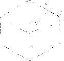
Figure 10 A and 10B show the structure of the dielectric resonator that discloses in the above-mentioned patent application, but only show essential part among the figure.In Figure 10 A and 10B, label 3 expressions one have the dielectric substrate of specific relative dielectric constant.Electrode 1 and 2 is formed on two first type surfaces of dielectric substrate, and each electrode all has the diameter of a circle by the non-electrode part of suitably determining 4 or 5.Conductive plate 17 and 18 is positioned at the both sides of dielectric substrate 3, with the dielectric substrate 3 one section suitable distance of being separated by.In this structure, in dielectric substrate 3, form columniform resonator area 60, it plays TE010 mould dielectric resonator.
In above-mentioned dielectric resonator structure, electrode is positioned on two opposed major surfaces of dielectric-slab, they have the essentially identical non-electrode part of shape, dielectric-slab is then between two conductive plates that separate each other, between its corresponding conductive plate of electrode on each dielectric-slab first type surface, produce TE mould extraneous wave (spuriouswave), and propagate in the space of this extraneous wave between dielectric-slab first type surface and conductive plate.Extraneous wave is reflected by the chamber wall, and produces standing wave thus.This means the resonance relevant with these standing waves can take place.
Propagate if produced in this TE mould extraneous wave and the extraneous wave space between each first type surface of dielectric-slab and conductive plate, so, the energy of TE010 mould resonator (this is most important in this dielectric resonator) can partly be converted to the energy of extraneous wave, thereby nonloaded Q (Qo) step-down and make deterioration in characteristics in the outer frequency range of band pass filter passband.
As disclosing in Japanese patent application 8-54452 number, applicant of the present invention has proposed a kind of technology, and this technology can be constructed dielectric resonator and the band pass filter that does not have the problems referred to above.
The communicator that an object of the present invention is to provide dielectric resonator, dielectric filter, duplexer and use this device has prevented the problems referred to above with the mode that is different from Japanese patent application 8-54452 number in these devices.
According to one aspect of the present invention, a kind of dielectric resonator is provided, it comprises electrode, they are formed on two first type surfaces of dielectric-slab; Non-electrode part, they have essentially identical shape and are formed in each electrode, cause non-electrode partly to be positioned on the corresponding mutually position of dielectric-slab corresponding main surfaces; Zone between non-electrode part is divided, play the resonance region, and non-electrode part is surrounded by the cavity that forms in the conductor box, dielectric resonator is characterised in that: the size of determining cavity, make the cut-off frequency of cavity be higher than the resonance frequency of resonance region, and the size that makes cavity is greater than the outside dimension of non-electrode part, thereby guarantees to produce extraneous wave in electrode on the first type surface of dielectric-slab and the space between the cavity inner wall.
In above-mentioned dielectric resonator, preferably cavity is made cylindrical, its interior diameter 2a a<c/ (3.412fo) that satisfies condition, wherein fo is the resonance frequency of resonance region, and c is the light velocity.
When cavity being used as radius and being the circular waveguide of a, the lowest order mode of circular waveguide is TE11, and its cut-off wavelength λ c is λ c=3.412a.Therefore, if select radius a, make it satisfy a<c/ (3.412fo), wherein fo is the resonance frequency of resonance region, and c is the light velocity, and the TE11 ripple ends so, thereby has suppressed the propagation of TE11 ripple in cavity.
Cavity can also be made rectangle, the width of the rectangle a<c/ (2fo) that satisfies condition, wherein fo is the resonance frequency of resonance region, and c is the light velocity.
When cavity was used as rectangular waveguide, the lowest order mode formula was TE10, and cut-off wavelength λ c is λ c=2a.Therefore, if select width a, make it satisfy a<c/ (2fo), wherein fo is the resonance frequency of resonance region, and c is the light velocity, and the TE10 ripple ends so, thereby has suppressed the propagation of TE10 ripple in cavity.
According to another aspect of the present invention, a kind of dielectric filter is provided, it comprises electrode, they are formed on two first type surfaces of dielectric-slab; A plurality of non-electrode parts, they have essentially identical shape, and are formed in each electrode, cause non-electrode on first type surface of dielectric-slab partly to be positioned on the corresponding position of each non-electrode part on another first type surface with opposite side; Each zone between non-electrode part is divided, play the resonance region, the cavity that described non-electrode part is formed in conductive box surrounds, dielectric filter also comprises a signal input part and a signal output element, these two parts all with a plurality of resonance regions near any zone electromagnetic field couples, dielectric filter is characterised in that, determine the cavity width of the boundary portion office between the adjacent non-electrode part branch like this, make the resonance frequency that is higher than the resonance region with the cut-off frequency of boundary-related, thereby guarantee to produce extraneous wave in electrode on the first type surface of dielectric-slab and the space between the cavity inner wall.Therefore, the dielectric filter of gained is very outstanding, and it can obtain bigger decay in the passband frequency range outward, and can suppress extraneous wave.
Can be adjusted in coupling between the adjacent resonators that forms in the corresponding resonance region by the width of suitably selecting cavity boundary part.
In this dielectric filter, preferably will be enclosed in cavity around the non-electrode part and make cylindrically, and determine like this width e of described cavity boundary part to make it satisfy e<c/ (2fo), wherein fo is the resonance frequency of resonance region, and c is the light velocity.
Cavity plays waveguide, and the cut-off frequency of its boundary portion office is c/ (2fo).Therefore,, make it satisfy e<c (2fo), so just can suppress extraneous wave and propagate by boundary member if select width e like this.
According to another aspect of the present invention, a kind of duplexer is provided, it is characterized in that, dielectric filter comprises one according to any one dielectric resonator of the present invention, and comprise signal input part and a signal output element, perhaps the dielectric filter according to the above-mentioned aspect of the present invention is used as emission filter or receiving filter, perhaps as receiving and emission filter, emission filter is placed on and transmits between input port and the input/output end port, and receiving filter is placed between received signal output port and the input/output end port.
Provide a kind of communicator more on the one hand according to of the present invention, it is characterized in that, it comprises a radio circuit, this radio circuit has the dielectric resonator according to any aspect of the present invention, according to the dielectric filter of any aspect of the present invention, or according to duplexer of the present invention.
Figure 1A and 1B are the schematic diagrames according to the dielectric resonator of first embodiment of the invention;
Fig. 2 A and 2B are the schematic diagrames according to the dielectric resonator of second embodiment of the invention;
Fig. 3 A and 3B are the schematic diagrames according to the dielectric filter of third embodiment of the invention;
Fig. 4 A and 4B show the characteristic curve of dielectric filter shown in Fig. 3 A, 3B, 9A and the 9B;
Fig. 5 A and 5B are the schematic diagrames according to the dielectric filter of fourth embodiment of the invention;
Fig. 6 A and 6B are the schematic diagrames according to the dielectric filter of fifth embodiment of the invention;
Fig. 7 A and 7B are the schematic diagrames according to the dielectric filter of sixth embodiment of the invention;
Fig. 8 A and 8B are the schematic diagrames according to the dielectric filter of seventh embodiment of the invention;
Fig. 9 A and 9B are the schematic diagrames according to the dielectric filter of conventional art;
Figure 10 A and 10B are the schematic diagram of illustration according to the dielectric resonator structure of conventional art, also show electromagnetic field distribution among the figure;
Figure 11 is the schematic diagram according to duplexer of the present invention;
Figure 12 shows the block diagram according to communicator of the present invention.
Hereinafter with reference to Figure 1A and 1B dielectric resonator according to first embodiment of the invention is described.Figure 1A is an outward appearance perspective view, and Figure 1B is its profile.In Figure 1A and 1B, label 3 expressions one dielectric-slab.On two first type surfaces of dielectric-slab 3, form electrode 1 and 2, and in electrode 1 and 2, form circular non-electrode part 4 and 5 respectively, non-electrode part 4 and 5 is laid respectively on the similar position of dielectric-slab 3 both sides.Resonance region 60 is played in the zone of dielectric-slab 3 between non-electrode part 4 and 5.Total is as a dielectric resonator of doing with the TE010 die worker.Dielectric substrate 3 is placed in the conductor 6, so that between conductor 6 and dielectric-slab 3, form cavity 8 and 9. Cavity 8 and 9 is made and non-electrode part 4 and 5 coaxial cylindrical.
When cavity 8 and 9 being used as interior diameter being the circular waveguide of 2a, the lowest order mode of these circular waveguides is TE11, and their cut-off wavelength λ c is:
λc=3.412a (1)
When the resonance frequency of representing resonance region 60 with fo, and when representing the light velocity, select the interior diameter 2a of cavity 8 and 9, it satisfied with c:
A<c/ (3.412fo) (2) thus guarantee that the cut-off frequency of TE11 mould is higher than the resonance frequency of resonance region 60.In addition, select interior diameter 2a, make its diameter d greater than non-electrode part 4 and 5.When the resonance frequency of resonator for example was 20GHz, inequality (2) became 2a<8.8mm.That is to say that cavity 8 and 9 interior diameter should be less than 8.8mm.In practice, elect cut-off frequency as above-mentioned theory value 1.5 to 2 times,, thereby guarantee not allow the main electromagnetic field of TE010 mould expand to (in other words, being about to electromagnetic field is limited in the dielectric-slab) in the cavity so that have enough big surplus.If elect cut-off frequency as theoretical value 1.5 times, cavity 8 and 9 interior diameter 2a are 5.8mm so.
Fig. 2 A and 2B show the structure according to the dielectric resonator of second embodiment of the invention.The difference of resonator is shown in this dielectric resonator and Figure 1A and the 1B, and the cavity 8 and 9 that forms between conductor 6 and the dielectric-slab 3 is a rectangle.When cavity 8 and 9 was used as rectangular waveguide, their lowest order mode was TE10, and cut-off wavelength λ c is:
λc=2a
When the resonance frequency of representing resonance region 60 with fo, and when representing the light velocity, select the inside dimension of cavity 8 and 9, it satisfied with c:
A<c/ (2fo) (3) thus guarantee that the cut-off frequency of TE10 mould is higher than the resonance frequency of resonance region 60.In addition, select the inside dimension a of cavity, make its diameter d greater than non-electrode part 4 and 5.When the resonance frequency of resonator for example was 20GHz, inequality (2) became a<7.5mm.That is to say that cavity 8 and 9 inside dimension should be less than 7.5mm.In practice, elect cut-off frequency as above-mentioned theory value 1.5 to 2 times, so that have enough big surplus.If elect cut-off frequency as theoretical value 1.5 times, cavity 8 and 9 inside dimension a are 5mm so.
Use aforesaid way, can suppress TE10 or TE11 mould extraneous wave by the size of selecting cavity, thereby the power conversion that prevents TE010 master's mould becomes spurious mode, prevents the deterioration of Qo thus.
Referring now to Fig. 3 A, 3B, 4A, 4B, 9A and 9B, the dielectric filter according to third embodiment of the invention is described.
Fig. 3 A and 3B are the profiles of expression dielectric filter internal structure, and wherein Fig. 3 A is the profile along B-B line intercepting among Fig. 3 B, and Fig. 3 B is the profile along A-A line intercepting among Fig. 3 A.In Fig. 3 A and 3B, label 3 expressions one dielectric-slab.Form electrode 1 and 2 on two first type surfaces of dielectric-slab 3, wherein each electrode all has non-electrode part 4a, 4b and the 4c that some circular diameters are d, or 5a, 5b and 5c.Non-electrode part 4a, 4b and 4c are positioned on the first type surface of dielectric-slab 3, but not electrode part 5a, 5b and 5c then lay respectively on the position corresponding with 4a, 4b and 4c on the corresponding main surfaces, thereby form three resonance region 60a, 60b and 60c.In Fig. 3 A and 3B, box of label 7 expressions, and label 16 expressions one substrate.Dielectric-slab 3 is placed in the box 7, and covers the opening of box with substrate 16.Between box and dielectric-slab 3, form cavity 8a, 8b and 8c, between dielectric-slab 3 and substrate 16, form cavity 9a, 9b and 9c, its cavity 8a, 8b and 8c are coaxial with non-electrode part 4a, 4b and 4c respectively, and cavity 9a, 9b and 9c are coaxial with non-electrode part 5a, 5b and 5c respectively.Cavity 8a, 8b and 8c are continuous at boundary, have width smaller e between the adjacent cavities.Equally, cavity 9a, 9b and 9c also are continuous at its boundary separately.
When the resonance frequency of representing resonance region 60a, 60b and 60c with fo, and when representing the light velocity, select the interior diameter 2a of cavity 8a, 8b, 8c, 9a, 9b and 9c, make it satisfy inequality (2), thereby the cut-off frequency of guaranteeing cavity is higher than resonance frequency fo with c.In addition, interior diameter 2a is chosen to greater than non-electrode diameter d partly.
When above-mentioned cavity was used as waveguide, width was that the cut-off wavelength λ c of the boundary of e is between adjacent cavities:
λc=2e (4)
Therefore, when the resonance frequency of resonance region is fo, if border width is arranged to less than c/ (2fo), just suppressed the TE10 mould extraneous wave propagated by cavity boundary so.For example, when fo=20GHz, e is chosen to less than 7.5mm.
Owing to can suppress extraneous wave by the width e of suitably selecting border between cavity as mentioned above, so, just needn't satisfy inequality (2) if satisfied equation (4).
In the structure shown in Fig. 3 A and the 3B, probe 10 and 11 respectively with resonance region 60a and 60c magnetic coupling. Adjacent resonance region 60a and 60b are magnetically coupling to one another by the space between the adjacent resonance region. Adjacent resonance region 60b and 60c also are magnetically coupling to one another in an identical manner.
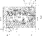
For comparing with the dielectric filter shown in Fig. 3 A and the 3B, a profile is provided in Fig. 9 A and 9B, they show the structure according to the dielectric filter of conventional art.Different with the dielectric filter shown in Fig. 3 A and the 3B, the upper and lower at dielectric-slab 3 forms cavity 8 and 9 in such a way, causes the shape of cavity wall similar to the outer wall of box 7.In Fig. 9 A and 9B, label 19 expressions one extraneous wave suppresses plate, its appropriate position between substrate 16 and electrode 2, wherein electrode 2 is formed at the lower surface of dielectric-slab 3, thus at electrode 2 and be provided with between the ground electrode of position that extraneous wave suppresses plate 19 and form a lc circuit (LC resonator).The technology of using this extraneous wave to suppress plate drops in the scope of above-mentioned Japanese patent application 8-54452 number.
Below list the size of the dielectric filter each several part shown in Fig. 3 A, 3B, 9A and the 9B, wherein also shown relative dielectric constant ε r.
Table 1
| Fig. 3 A, 3B | Fig. 9 A, 9B | |
| Interior diameter 2a | 5.5 | - |
| Width a | - | 8.0 |
| h1 | 1.0 | 1.5 |
| h2 | 1.0 | 2.0 |
| t | 1.0 | 1.0 |
| g | 0.5 | 0.7 |
| εr | 30 | 30 |
| d | 4.4 | 4.0 |
| e | 2.5 | - |
| b | 15.3 | 18.0 |
Fig. 4 A and 4B show the decay-frequency characteristic of the two media filter shown in Fig. 3 A and 3B, 9A and the 9B, and wherein Fig. 4 A shows the characteristic of Fig. 3 A and 3B medium filter, and Fig. 4 B shows the characteristic of Fig. 9 A and 9B medium filter.
In the dielectric filter shown in Fig. 9 A and the 9B, when the length b along the length limit of box 7 is used as the width of waveguide, can produce the low order resonance of TE10 mould along this direction of waveguide.In this concrete example, b=18.0 is so the cut-off frequency of TE10 mould is 8.3GHz.In fact, shown in Fig. 4 B, the resonance peak corresponding with this cut-off frequency appears in the scope of 9-9GHz.When the length a along the minor face of box 7 is used as the width of waveguide, because a=8.0 is fc=18.8GHz so can calculate the cut-off frequency of TE10 mould.But in Fig. 4 B, at this frequency place decay has appearred.This is because the lc circuit that suppresses plate 19 formation with extraneous wave shown in Fig. 9 A plays a part trapper, it signal trap in the scope of 18-20GHz.If do not provide extraneous wave to suppress plate, the resonance of TE10 pattern can appear near the 18.8GHz so, and near the frequency range the 18.8GHz then becomes a passband, the effect of TE010 mode filter thereby filter does not recur.
Under the situation of dielectric filter shown in Fig. 3 A and the 3B, as a whole if hypothesis is that the cavity of 15.3mm is done to total length b, role is the waveguide of 15.3mm as width, and the resonance of TE10 pattern can occur near the 9.8GHz so.Yet the interior shape of box forms in such a way, and it is similar to the shape of TE010 mould resonator part, so width e is little of 2.5mm.As a result, the fc of TE10 mould is higher than 30GHz, and shown in Fig. 4 A, can obtain the decay greater than 70 decibels in the frequency range of 9-11GHz.On the other hand, the cut-off frequency fc relevant with TE11 mould resonance that can be calculated corresponding to Fig. 3 A and the 2a of diameter shown in the 3B by inequality (2) and 2a=5.5mm is about 32GHz.Therefore, as seen, the resonance of this mould is unaffected from Fig. 4 A.
Therefore, in the structure shown in Fig. 3 A and the 3B, in the wide frequency range of DC to 25GHz, except resonance peak, can obtain decay greater than 40 decibels corresponding to the spurious resonance of HE110, HE210, HE310 and TE110 mould (they appear in the resonance region).
As seen from the above description, if shown in Fig. 3 A and 3B, determine the internal structure and the size of box, cut-off frequency can drop in the frequency range of being considered so, needn't use the extraneous wave shown in Fig. 9 A and 9B to suppress plate, and be easy to realize having the filter of desirable characteristics thus.This makes can make filter with the less parts of number.The minimizing of part count can reduce production costs, and improves reliability.
Referring now to Fig. 5 A and 5B, the dielectric filter according to fourth embodiment of the invention is described.In this embodiment, different with the structure shown in Fig. 3 A and the 3B, respectively at the upper and lower sides formation cavity 8 and 9 of dielectric-slab 3, cause cavity 8 and 9 on the whole length of the cavity that is provided with three resonance region 60a, 60b and 60c, to have fixing width a in such a way.So select width a, make it satisfy above-mentioned inequality (3).In addition, select the width a of cavity, make its diameter d greater than non-electrode part.Remaining parts is similar to the part shown in Fig. 3 A and the 3B.
Fig. 6 A and 6B show the structure according to the dielectric filter of fifth embodiment of the invention.With the difference of filter shown in Fig. 5 A and the 5B in, cavity 8a, 8b and 8c are formed at the top of resonance region 60a, 60b and 60c respectively, and cavity 9a, 9b and 9c are formed at the below of resonance region 60a, 60b and 60c respectively, wherein make the boundary member between the adjacent cavities narrow to width b.Remaining parts is similar to the part shown in Fig. 5 A and the 5B.By making the boundary member between the adjacent cavities narrow to width b, further suppressed extraneous wave by the propagation of boundary member in cavity.By changing the width b of narrowed portion, can regulate the coupling between the adjacent resonance region.That is to say that if reduce width b and keep the spacing between the adjacent non-electrode part branch constant, the coupling between the so adjacent resonance region can reduce.On the contrary, if increase width b, the coupling between the so adjacent resonance region can increase.
Fig. 7 A and 7B are the profiles according to the structure of the dielectric filter of sixth embodiment of the invention.Be that with the difference of Fig. 5 A and Fig. 5 B non-electrode part 4a, 4b, 4c, 5a, 5b and 5c are made into rectangle, and probe 10 and 11 is formed in the shape that extends to its end on the whole length as the crow flies.Similar shown in remaining parts and Fig. 5 A and the 5B.If non-electrode is partly made rectangle, each resonance region 60a, 60b and 60c play TE100 mould dielectric resonator so.Probe 10 and 11 respectively in resonance region 60a and 60c with the resonator magnetic coupling.Adjacent resonators among resonance region 60a and the 60c is magnetically coupling to one another.Equally, the adjacent resonators among resonance region 60b and the 60c also is magnetically coupling to one another.
Fig. 8 A and 8B are the profiles according to the structure of the dielectric filter of seventh embodiment of the invention.Be with the difference of Fig. 7 A and Fig. 7 B, cavity 8a, 8b and 8c are formed at the top of resonance region 60a, 60b and 60c respectively, and cavity 9a, 9b and 9c are formed at the below of resonance region 60a, 60b and 60c respectively, and wherein the boundary member between the adjacent cavities narrows down.Similar shown in remaining parts and Fig. 7 A and the 7B.By the boundary member between adjacent cavities is narrowed down, further suppressed extraneous wave by the propagation of boundary member in cavity.By changing the width of narrowed portion, can regulate the coupling between the adjacent resonators.
Referring now to Figure 11, the duplexer according to eighth embodiment of the invention is described.
Cross section shown in Figure 11 is to get along the planar interception that passes box 7 extensions with being similar to the mode shown in Fig. 3 A and the 3B.Its general structure is identical with the dual-port dielectric filter shown in Fig. 3 A and the 3B basically.On the upper surface of dielectric-slab, form an electrode, make this electrode have six non-electrode part 4a, 4b, 4c, 4d, 4e and 4f.On the lower surface of dielectric-slab, form a similar electrode, the non-electrode of bottom electrode partly is positioned on the position corresponding with the non-electrode part of top electrode.In this structure, six dielectric resonators are formed on the single dielectric-slab.
Form a receiving filter with three resonance region 60a, 60b being positioned at a side and 60c, and with its excess-three that is positioned at opposite side resonance region 60d, 60e and emission filter of 60f formation.The part of box 7 is at the resonance region 60c that plays the effect of the receiving filter first order and play between the resonance region 60d of emission filter final stage effect and extend, and isolates well each other so that guarantee receiving filter and emission filter.
Selection to the electrical length of the breakout of probe 11 and 20, is the odd-multiple of 1/4 wavelength of the tranmitting frequency that records from the equivalent short circuit plane of resonance region 60c on transmission line.Selection to the electrical length of the breakout of probe 11 and 20, is the odd-multiple of 1/4 wavelength of the receive frequency that records from the equivalent short circuit plane of resonance region 60d on transmission line.
This structure can make to transmit separates with received signal, and suppresses extraneous wave propagation in the space about dielectric-slab simultaneously in receiving filter and emission filter.
Figure 12 shows the block diagram according to the communicator of ninth embodiment of the invention.
In this communicator shown in Figure 12, the duplexer according to above-mentioned the 8th embodiment is used as antenna diplexer.In Figure 12, label 46a and 46b represent receiving filter and emission filter respectively, and they form an antenna diplexer 46.As shown in figure 12, receiving circuit 47 links to each other with the received signal output port 46c of antenna diplexer 46, and radiating circuit 48 links to each other with the port 46d that transmits.In addition, antenna 49 links to each other with input/output end port 46e, causes total to play communicator 50.
By using, can realize high performance miniaturization communicator at the antenna diplexer that has good characteristic aspect parasitism inhibition and emission, the received signal separation.
Although in the embodiment shown in fig. 12, in communicator, used according to duplexer of the present invention, in the radio circuit of communicator, can use any according to dielectric resonator of the present invention or dielectric filter.This makes it possible to achieve such communicator, and the radio circuit of this communicator has lower ghost effect.
As seen from the above description, the present invention has the following advantages. In according to resonator of the present invention, suppressed between the first type surface of cavity inner wall and electrode and dielectric-slab, to produce extraneous wave in the space. As a result, suppress the transfer of energy to spurious mode, thereby stoped the reduction of the nonloaded Q of dielectric resonator.
In addition, select the shape of cavity, thereby suppressed the generation of extraneous wave in more effective mode.
In according to wave filter of the present invention, suppressed extraneous wave, and prevented the deteriorated of attenuation characteristic in the outer frequency range of passband.
In according to duplexer of the present invention, obtained good attenuation characteristic in the frequency range outside passband.
In according to communicator of the present invention, in the radio circuit of communicator, obtained the superperformance that not affected by ghost effect. The communicator size of gained is little, and efficient is high.
Claims (3)
1. dielectric resonator, it comprises: electrode, they are formed on two first type surfaces of a dielectric-slab; Non-electrode part, they are of similar shape and are formed in each described electrode, cause described non-electrode partly to be positioned on the corresponding mutually position of dielectric-slab corresponding main surfaces; One zone, it plays the resonance region between described non-electrode part is divided, and described non-electrode part is surrounded by the cavity that forms in a conductor box, and described dielectric resonator is characterised in that:
So determine the size of described cavity, make the cut-off frequency of described cavity be higher than the resonance frequency of described resonance region, and make the outside dimension of the size of described cavity greater than described non-electrode part.
2. dielectric resonator as claimed in claim 1 is characterized in that, described cavity is made cylindrical, the described columniform interior diameter 2a a<c/ (3.412fo) that satisfies condition, wherein fo is the resonance frequency of described resonance region, and c is the light velocity.
3. dielectric resonator as claimed in claim 1 is characterized in that, described cavity is made rectangle, the width a of the described rectangle a<c/ (2fo) that satisfies condition, and wherein fo is the resonance frequency of described resonance region, and c is the light velocity.
Applications Claiming Priority (6)
| Application Number | Priority Date | Filing Date | Title |
|---|---|---|---|
| JP129614/1997 | 1997-05-20 | ||
| JP12961497 | 1997-05-20 | ||
| JP129614/97 | 1997-05-20 | ||
| JP113296/1998 | 1998-04-23 | ||
| JP113296/98 | 1998-04-23 | ||
| JP10113296A JPH1141002A (en) | 1997-05-20 | 1998-04-23 | Dielectric resonator, dielectric filter, and transmission/ reception common unit and communication device |
Related Child Applications (1)
| Application Number | Title | Priority Date | Filing Date |
|---|---|---|---|
| CN03120239A Division CN1445881A (en) | 1997-05-20 | 2003-03-04 | Dielectric resonator, dielectric filter, duplexer and communication device |
Publications (2)
| Publication Number | Publication Date |
|---|---|
| CN1199937A CN1199937A (en) | 1998-11-25 |
| CN1120540C true CN1120540C (en) | 2003-09-03 |
Family
ID=26452292
Family Applications (2)
| Application Number | Title | Priority Date | Filing Date |
|---|---|---|---|
| CN98109277A Expired - Fee Related CN1120540C (en) | 1997-05-20 | 1998-05-20 | Dielectric resonator, dielectric filter, duplexer, and communication device |
| CN03120239A Pending CN1445881A (en) | 1997-05-20 | 2003-03-04 | Dielectric resonator, dielectric filter, duplexer and communication device |
Family Applications After (1)
| Application Number | Title | Priority Date | Filing Date |
|---|---|---|---|
| CN03120239A Pending CN1445881A (en) | 1997-05-20 | 2003-03-04 | Dielectric resonator, dielectric filter, duplexer and communication device |
Country Status (7)
| Country | Link |
|---|---|
| US (2) | US6104261A (en) |
| EP (1) | EP0880191B1 (en) |
| JP (1) | JPH1141002A (en) |
| KR (1) | KR100287258B1 (en) |
| CN (2) | CN1120540C (en) |
| CA (1) | CA2238126C (en) |
| DE (1) | DE69829708D1 (en) |
Families Citing this family (17)
| Publication number | Priority date | Publication date | Assignee | Title |
|---|---|---|---|---|
| JPH1141002A (en) * | 1997-05-20 | 1999-02-12 | Murata Mfg Co Ltd | Dielectric resonator, dielectric filter, and transmission/ reception common unit and communication device |
| JP3353717B2 (en) * | 1998-09-07 | 2002-12-03 | 株式会社村田製作所 | Dielectric filter, dielectric duplexer and communication device |
| JP3506077B2 (en) * | 1999-11-24 | 2004-03-15 | 株式会社村田製作所 | Multi-mode dielectric resonator device, filter, duplexer, and communication device |
| JP3506076B2 (en) * | 1999-11-24 | 2004-03-15 | 株式会社村田製作所 | Multi-mode dielectric resonator device, filter, duplexer, and communication device |
| JP2002330001A (en) | 2001-05-02 | 2002-11-15 | Murata Mfg Co Ltd | Band-pass filter and communication equipment |
| FR2850792A1 (en) * | 2003-02-03 | 2004-08-06 | Thomson Licensing Sa | COMPACT WAVEGUIDE FILTER |
| CN1322629C (en) * | 2003-11-13 | 2007-06-20 | 京瓷株式会社 | Dielectric medium resonator, dielectric medium filter and radio communication device |
| US7280010B2 (en) * | 2005-03-31 | 2007-10-09 | U.S. Monolithics, L.L.C. | Dielectric resonator RF interconnect |
| US20100209929A1 (en) * | 2009-01-14 | 2010-08-19 | Nodality, Inc., A Delaware Corporation | Multiple mechanisms for modulation of jak/stat activity |
| CN101572335B (en) * | 2009-06-05 | 2013-10-09 | 北京航空航天大学 | K-waveband dielectric disk-loaded circular waveguide feed filter |
| US9077062B2 (en) * | 2012-03-02 | 2015-07-07 | Lockheed Martin Corporation | System and method for providing an interchangeable dielectric filter within a waveguide |
| US10324314B2 (en) * | 2017-05-24 | 2019-06-18 | Uchicago Argonne, Llc | Ultra-flat optical device with high transmission efficiency |
| US10613254B2 (en) | 2017-05-24 | 2020-04-07 | Uchicago Argonne, Llc | Ultrathin, polarization-independent, achromatic metalens for focusing visible light |
| CN111384495A (en) * | 2018-12-29 | 2020-07-07 | 深圳市大富科技股份有限公司 | Dielectric filter and communication equipment |
| CN111384550A (en) * | 2018-12-29 | 2020-07-07 | 深圳市大富科技股份有限公司 | Filter and communication device |
| US11437691B2 (en) | 2019-06-26 | 2022-09-06 | Cts Corporation | Dielectric waveguide filter with trap resonator |
| CN112821021B (en) * | 2021-01-22 | 2022-05-17 | 华沣通信科技有限公司 | Sheet welding type small filter and manufacturing method thereof |
Family Cites Families (10)
| Publication number | Priority date | Publication date | Assignee | Title |
|---|---|---|---|---|
| US4675631A (en) * | 1985-01-17 | 1987-06-23 | M/A-Com, Inc. | Waveguide bandpass filter |
| JPS61245606A (en) * | 1985-04-23 | 1986-10-31 | Alps Electric Co Ltd | Microwave oscillator |
| JPH0652841B2 (en) * | 1988-02-15 | 1994-07-06 | 株式会社村田製作所 | Resonator device |
| US5220300A (en) * | 1992-04-15 | 1993-06-15 | Rs Microwave Company, Inc. | Resonator filters with wide stopbands |
| JP2897678B2 (en) * | 1995-03-22 | 1999-05-31 | 株式会社村田製作所 | Dielectric resonator and high-frequency band-pass filter device |
| JP2897117B2 (en) * | 1995-09-19 | 1999-05-31 | 株式会社村田製作所 | Variable frequency dielectric resonator |
| JP3603453B2 (en) * | 1996-03-12 | 2004-12-22 | 株式会社村田製作所 | Dielectric resonator and bandpass filter |
| JP3087664B2 (en) * | 1996-11-06 | 2000-09-11 | 株式会社村田製作所 | Dielectric resonator device and high frequency module |
| JP3589008B2 (en) * | 1997-04-18 | 2004-11-17 | 株式会社村田製作所 | Dielectric resonator, filter using the same, duplexer, and communication device |
| JPH1141002A (en) * | 1997-05-20 | 1999-02-12 | Murata Mfg Co Ltd | Dielectric resonator, dielectric filter, and transmission/ reception common unit and communication device |
-
1998
- 1998-04-23 JP JP10113296A patent/JPH1141002A/en active Pending
- 1998-05-19 DE DE69829708T patent/DE69829708D1/en not_active Expired - Fee Related
- 1998-05-19 EP EP98109125A patent/EP0880191B1/en not_active Expired - Lifetime
- 1998-05-20 US US09/081,806 patent/US6104261A/en not_active Expired - Fee Related
- 1998-05-20 CA CA002238126A patent/CA2238126C/en not_active Expired - Fee Related
- 1998-05-20 KR KR1019980018181A patent/KR100287258B1/en not_active IP Right Cessation
- 1998-05-20 CN CN98109277A patent/CN1120540C/en not_active Expired - Fee Related
-
2000
- 2000-05-08 US US09/567,291 patent/US6445263B1/en not_active Expired - Fee Related
-
2003
- 2003-03-04 CN CN03120239A patent/CN1445881A/en active Pending
Also Published As
| Publication number | Publication date |
|---|---|
| JPH1141002A (en) | 1999-02-12 |
| KR19980087229A (en) | 1998-12-05 |
| DE69829708D1 (en) | 2005-05-19 |
| EP0880191B1 (en) | 2005-04-13 |
| US6445263B1 (en) | 2002-09-03 |
| CA2238126C (en) | 2001-03-20 |
| CN1445881A (en) | 2003-10-01 |
| KR100287258B1 (en) | 2001-04-16 |
| CA2238126A1 (en) | 1998-11-20 |
| US6104261A (en) | 2000-08-15 |
| CN1199937A (en) | 1998-11-25 |
| EP0880191A1 (en) | 1998-11-25 |
Similar Documents
| Publication | Publication Date | Title |
|---|---|---|
| CN1120540C (en) | Dielectric resonator, dielectric filter, duplexer, and communication device | |
| CN1172405C (en) | High-frequency transmission line, dielectric resonator, filter, duplexer, and communication device | |
| CN102696145B (en) | Microwave transition device between a microstrip line and a rectangular waveguide | |
| US7154441B2 (en) | Device for transmitting or emitting high-frequency waves | |
| US7299534B2 (en) | Method of fabrication of low-loss filter and frequency multiplexer | |
| CN102013537A (en) | Substrate integrated waveguide split ring resonator-based microwave band pass filter | |
| CN1134085C (en) | Dielectric resonator device | |
| CN1169256C (en) | Filter device, duplexer and communication device | |
| CN1140007C (en) | Medium filter, antenna shared device and communication equipment | |
| CN1120542C (en) | Planar dielectric line and integrated circuit using the same | |
| CN1768445A (en) | Ultra-thin type ceramic RF filter | |
| KR100611485B1 (en) | Line converter, high-frequency module, and communication device | |
| CN1221995A (en) | Dielectric filter, dielectrie duplexer, and communication device | |
| TWI741840B (en) | Dielectric waveguide filter | |
| CN1147961C (en) | Dielectric filter, dielectric duplexer and communication equipment using the same | |
| CN1135647C (en) | Dielectric filter and communication apparatus using same | |
| CN1160825C (en) | Dielectric filter, dielectric duplexer and communication equipment containing them | |
| CN1144315C (en) | Medium wave filber, receiving-sending shared device and communication apparatus | |
| US6483405B1 (en) | Dielectric filter, duplexer and communication apparatus | |
| CN1326270A (en) | Coaxial resonator, filter, duplexer and communication device | |
| CN113794061B (en) | Ultra-wideband single-layer slot array antenna based on slot gap waveguide | |
| CN1180511C (en) | Dielectric filter, dielectric diplexer and communication device | |
| CN214706200U (en) | Band-pass filter for high-power circuit reading | |
| CN1438732A (en) | Electric Medium resonator, electric medium wave filter, electric medium diplexer and communication device | |
| Li et al. | Design of Crossover Based on Printed Gap Waveguide for Millimeter-wave Application |
Legal Events
| Date | Code | Title | Description |
|---|---|---|---|
| C10 | Entry into substantive examination | ||
| SE01 | Entry into force of request for substantive examination | ||
| C06 | Publication | ||
| PB01 | Publication | ||
| C14 | Grant of patent or utility model | ||
| GR01 | Patent grant | ||
| C17 | Cessation of patent right | ||
| CF01 | Termination of patent right due to non-payment of annual fee |
Granted publication date: 20030903 |