CN111697119A - LED using luminescent sapphire as down-converter - Google Patents
LED using luminescent sapphire as down-converter Download PDFInfo
- Publication number
- CN111697119A CN111697119A CN202010564496.0A CN202010564496A CN111697119A CN 111697119 A CN111697119 A CN 111697119A CN 202010564496 A CN202010564496 A CN 202010564496A CN 111697119 A CN111697119 A CN 111697119A
- Authority
- CN
- China
- Prior art keywords
- sapphire
- led
- light
- luminescent
- luminescent sapphire
- Prior art date
- Legal status (The legal status is an assumption and is not a legal conclusion. Google has not performed a legal analysis and makes no representation as to the accuracy of the status listed.)
- Pending
Links
- 239000010980 sapphire Substances 0.000 title claims abstract description 147
- 229910052594 sapphire Inorganic materials 0.000 title claims abstract description 142
- OAICVXFJPJFONN-UHFFFAOYSA-N Phosphorus Chemical compound [P] OAICVXFJPJFONN-UHFFFAOYSA-N 0.000 claims abstract description 51
- 239000000758 substrate Substances 0.000 claims abstract description 36
- 230000003287 optical effect Effects 0.000 claims abstract description 27
- 239000000203 mixture Substances 0.000 claims abstract description 21
- 239000004065 semiconductor Substances 0.000 claims abstract description 18
- 238000000137 annealing Methods 0.000 claims abstract description 17
- 239000002245 particle Substances 0.000 claims abstract description 10
- 239000011230 binding agent Substances 0.000 claims abstract description 8
- 239000010410 layer Substances 0.000 claims description 88
- 238000010521 absorption reaction Methods 0.000 claims description 24
- 239000013078 crystal Substances 0.000 claims description 17
- 238000000034 method Methods 0.000 claims description 12
- QVGXLLKOCUKJST-UHFFFAOYSA-N atomic oxygen Chemical compound [O] QVGXLLKOCUKJST-UHFFFAOYSA-N 0.000 claims description 8
- 229910052760 oxygen Inorganic materials 0.000 claims description 8
- 239000001301 oxygen Substances 0.000 claims description 8
- 229910052731 fluorine Inorganic materials 0.000 claims description 6
- 238000004020 luminiscence type Methods 0.000 claims description 5
- 239000012790 adhesive layer Substances 0.000 claims description 4
- 230000003213 activating effect Effects 0.000 claims 1
- 239000011777 magnesium Substances 0.000 description 16
- 238000006243 chemical reaction Methods 0.000 description 14
- 230000004913 activation Effects 0.000 description 10
- PNEYBMLMFCGWSK-UHFFFAOYSA-N aluminium oxide Inorganic materials [O-2].[O-2].[O-2].[Al+3].[Al+3] PNEYBMLMFCGWSK-UHFFFAOYSA-N 0.000 description 9
- 229910052593 corundum Inorganic materials 0.000 description 9
- 239000000843 powder Substances 0.000 description 9
- 238000013500 data storage Methods 0.000 description 8
- 229920001296 polysiloxane Polymers 0.000 description 8
- 230000008569 process Effects 0.000 description 8
- 229910001845 yogo sapphire Inorganic materials 0.000 description 8
- 238000004519 manufacturing process Methods 0.000 description 7
- 230000003750 conditioning effect Effects 0.000 description 6
- 238000000151 deposition Methods 0.000 description 6
- 230000001965 increasing effect Effects 0.000 description 6
- 229910052751 metal Inorganic materials 0.000 description 6
- 239000002184 metal Substances 0.000 description 6
- 150000001768 cations Chemical class 0.000 description 5
- 230000010354 integration Effects 0.000 description 5
- 239000000463 material Substances 0.000 description 5
- 238000012360 testing method Methods 0.000 description 5
- 238000004220 aggregation Methods 0.000 description 4
- 230000007423 decrease Effects 0.000 description 4
- 238000009826 distribution Methods 0.000 description 4
- 230000005284 excitation Effects 0.000 description 4
- 230000002776 aggregation Effects 0.000 description 3
- 239000012298 atmosphere Substances 0.000 description 3
- 230000007547 defect Effects 0.000 description 3
- 230000008021 deposition Effects 0.000 description 3
- 238000000605 extraction Methods 0.000 description 3
- 238000011049 filling Methods 0.000 description 3
- TWNQGVIAIRXVLR-UHFFFAOYSA-N oxo(oxoalumanyloxy)alumane Chemical compound O=[Al]O[Al]=O TWNQGVIAIRXVLR-UHFFFAOYSA-N 0.000 description 3
- 238000012545 processing Methods 0.000 description 3
- 239000000654 additive Substances 0.000 description 2
- 239000000853 adhesive Substances 0.000 description 2
- 230000001070 adhesive effect Effects 0.000 description 2
- 230000008901 benefit Effects 0.000 description 2
- 239000011248 coating agent Substances 0.000 description 2
- 238000000576 coating method Methods 0.000 description 2
- 239000003086 colorant Substances 0.000 description 2
- 230000006378 damage Effects 0.000 description 2
- 239000002019 doping agent Substances 0.000 description 2
- 238000004980 dosimetry Methods 0.000 description 2
- 230000004907 flux Effects 0.000 description 2
- 239000011521 glass Substances 0.000 description 2
- 238000003384 imaging method Methods 0.000 description 2
- 239000011159 matrix material Substances 0.000 description 2
- 239000002096 quantum dot Substances 0.000 description 2
- 239000007787 solid Substances 0.000 description 2
- 229910052712 strontium Inorganic materials 0.000 description 2
- 239000000126 substance Substances 0.000 description 2
- 238000002231 Czochralski process Methods 0.000 description 1
- 239000004593 Epoxy Substances 0.000 description 1
- YCKRFDGAMUMZLT-UHFFFAOYSA-N Fluorine atom Chemical compound [F] YCKRFDGAMUMZLT-UHFFFAOYSA-N 0.000 description 1
- 241001530119 Vaccaria Species 0.000 description 1
- 239000012190 activator Substances 0.000 description 1
- 229910052788 barium Inorganic materials 0.000 description 1
- 239000007767 bonding agent Substances 0.000 description 1
- 229910052791 calcium Inorganic materials 0.000 description 1
- 150000001875 compounds Chemical class 0.000 description 1
- 238000007796 conventional method Methods 0.000 description 1
- 239000010431 corundum Substances 0.000 description 1
- 230000001186 cumulative effect Effects 0.000 description 1
- 238000005520 cutting process Methods 0.000 description 1
- 238000005137 deposition process Methods 0.000 description 1
- 239000002270 dispersing agent Substances 0.000 description 1
- 239000006185 dispersion Substances 0.000 description 1
- 230000000694 effects Effects 0.000 description 1
- 238000001962 electrophoresis Methods 0.000 description 1
- 238000000295 emission spectrum Methods 0.000 description 1
- 238000005538 encapsulation Methods 0.000 description 1
- 238000005516 engineering process Methods 0.000 description 1
- 230000001747 exhibiting effect Effects 0.000 description 1
- 239000011737 fluorine Substances 0.000 description 1
- 238000000227 grinding Methods 0.000 description 1
- 238000010438 heat treatment Methods 0.000 description 1
- 239000012535 impurity Substances 0.000 description 1
- 238000010030 laminating Methods 0.000 description 1
- 230000031700 light absorption Effects 0.000 description 1
- 229910052749 magnesium Inorganic materials 0.000 description 1
- 238000002156 mixing Methods 0.000 description 1
- 238000012634 optical imaging Methods 0.000 description 1
- 230000001590 oxidative effect Effects 0.000 description 1
- 238000005498 polishing Methods 0.000 description 1
- 230000005855 radiation Effects 0.000 description 1
- 230000000191 radiation effect Effects 0.000 description 1
- 230000009467 reduction Effects 0.000 description 1
- 238000005245 sintering Methods 0.000 description 1
- 238000001228 spectrum Methods 0.000 description 1
- 238000005507 spraying Methods 0.000 description 1
- 230000000638 stimulation Effects 0.000 description 1
- 239000010409 thin film Substances 0.000 description 1
- 238000001429 visible spectrum Methods 0.000 description 1
Images


Classifications
-
- H—ELECTRICITY
- H01—ELECTRIC ELEMENTS
- H01L—SEMICONDUCTOR DEVICES NOT COVERED BY CLASS H10
- H01L33/00—Semiconductor devices with at least one potential-jump barrier or surface barrier specially adapted for light emission; Processes or apparatus specially adapted for the manufacture or treatment thereof or of parts thereof; Details thereof
- H01L33/48—Semiconductor devices with at least one potential-jump barrier or surface barrier specially adapted for light emission; Processes or apparatus specially adapted for the manufacture or treatment thereof or of parts thereof; Details thereof characterised by the semiconductor body packages
- H01L33/50—Wavelength conversion elements
- H01L33/501—Wavelength conversion elements characterised by the materials, e.g. binder
- H01L33/502—Wavelength conversion materials
- H01L33/504—Elements with two or more wavelength conversion materials
-
- H—ELECTRICITY
- H01—ELECTRIC ELEMENTS
- H01L—SEMICONDUCTOR DEVICES NOT COVERED BY CLASS H10
- H01L33/00—Semiconductor devices with at least one potential-jump barrier or surface barrier specially adapted for light emission; Processes or apparatus specially adapted for the manufacture or treatment thereof or of parts thereof; Details thereof
- H01L33/005—Processes
- H01L33/0095—Post-treatment of devices, e.g. annealing, recrystallisation or short-circuit elimination
-
- H—ELECTRICITY
- H01—ELECTRIC ELEMENTS
- H01L—SEMICONDUCTOR DEVICES NOT COVERED BY CLASS H10
- H01L33/00—Semiconductor devices with at least one potential-jump barrier or surface barrier specially adapted for light emission; Processes or apparatus specially adapted for the manufacture or treatment thereof or of parts thereof; Details thereof
- H01L33/005—Processes
- H01L33/0062—Processes for devices with an active region comprising only III-V compounds
- H01L33/0075—Processes for devices with an active region comprising only III-V compounds comprising nitride compounds
-
- H—ELECTRICITY
- H01—ELECTRIC ELEMENTS
- H01L—SEMICONDUCTOR DEVICES NOT COVERED BY CLASS H10
- H01L33/00—Semiconductor devices with at least one potential-jump barrier or surface barrier specially adapted for light emission; Processes or apparatus specially adapted for the manufacture or treatment thereof or of parts thereof; Details thereof
- H01L33/02—Semiconductor devices with at least one potential-jump barrier or surface barrier specially adapted for light emission; Processes or apparatus specially adapted for the manufacture or treatment thereof or of parts thereof; Details thereof characterised by the semiconductor bodies
- H01L33/025—Physical imperfections, e.g. particular concentration or distribution of impurities
-
- H—ELECTRICITY
- H01—ELECTRIC ELEMENTS
- H01L—SEMICONDUCTOR DEVICES NOT COVERED BY CLASS H10
- H01L33/00—Semiconductor devices with at least one potential-jump barrier or surface barrier specially adapted for light emission; Processes or apparatus specially adapted for the manufacture or treatment thereof or of parts thereof; Details thereof
- H01L33/02—Semiconductor devices with at least one potential-jump barrier or surface barrier specially adapted for light emission; Processes or apparatus specially adapted for the manufacture or treatment thereof or of parts thereof; Details thereof characterised by the semiconductor bodies
- H01L33/26—Materials of the light emitting region
- H01L33/30—Materials of the light emitting region containing only elements of group III and group V of the periodic system
- H01L33/32—Materials of the light emitting region containing only elements of group III and group V of the periodic system containing nitrogen
-
- H—ELECTRICITY
- H01—ELECTRIC ELEMENTS
- H01L—SEMICONDUCTOR DEVICES NOT COVERED BY CLASS H10
- H01L33/00—Semiconductor devices with at least one potential-jump barrier or surface barrier specially adapted for light emission; Processes or apparatus specially adapted for the manufacture or treatment thereof or of parts thereof; Details thereof
- H01L33/48—Semiconductor devices with at least one potential-jump barrier or surface barrier specially adapted for light emission; Processes or apparatus specially adapted for the manufacture or treatment thereof or of parts thereof; Details thereof characterised by the semiconductor body packages
- H01L33/50—Wavelength conversion elements
- H01L33/501—Wavelength conversion elements characterised by the materials, e.g. binder
- H01L33/502—Wavelength conversion materials
-
- H—ELECTRICITY
- H01—ELECTRIC ELEMENTS
- H01L—SEMICONDUCTOR DEVICES NOT COVERED BY CLASS H10
- H01L33/00—Semiconductor devices with at least one potential-jump barrier or surface barrier specially adapted for light emission; Processes or apparatus specially adapted for the manufacture or treatment thereof or of parts thereof; Details thereof
- H01L33/48—Semiconductor devices with at least one potential-jump barrier or surface barrier specially adapted for light emission; Processes or apparatus specially adapted for the manufacture or treatment thereof or of parts thereof; Details thereof characterised by the semiconductor body packages
- H01L33/50—Wavelength conversion elements
- H01L33/507—Wavelength conversion elements the elements being in intimate contact with parts other than the semiconductor body or integrated with parts other than the semiconductor body
-
- H—ELECTRICITY
- H01—ELECTRIC ELEMENTS
- H01L—SEMICONDUCTOR DEVICES NOT COVERED BY CLASS H10
- H01L33/00—Semiconductor devices with at least one potential-jump barrier or surface barrier specially adapted for light emission; Processes or apparatus specially adapted for the manufacture or treatment thereof or of parts thereof; Details thereof
- H01L33/48—Semiconductor devices with at least one potential-jump barrier or surface barrier specially adapted for light emission; Processes or apparatus specially adapted for the manufacture or treatment thereof or of parts thereof; Details thereof characterised by the semiconductor body packages
- H01L33/52—Encapsulations
- H01L33/54—Encapsulations having a particular shape
-
- H—ELECTRICITY
- H01—ELECTRIC ELEMENTS
- H01L—SEMICONDUCTOR DEVICES NOT COVERED BY CLASS H10
- H01L2933/00—Details relating to devices covered by the group H01L33/00 but not provided for in its subgroups
- H01L2933/0008—Processes
- H01L2933/0033—Processes relating to semiconductor body packages
- H01L2933/0041—Processes relating to semiconductor body packages relating to wavelength conversion elements
-
- H—ELECTRICITY
- H01—ELECTRIC ELEMENTS
- H01L—SEMICONDUCTOR DEVICES NOT COVERED BY CLASS H10
- H01L2933/00—Details relating to devices covered by the group H01L33/00 but not provided for in its subgroups
- H01L2933/0008—Processes
- H01L2933/0033—Processes relating to semiconductor body packages
- H01L2933/005—Processes relating to semiconductor body packages relating to encapsulations
-
- H—ELECTRICITY
- H01—ELECTRIC ELEMENTS
- H01L—SEMICONDUCTOR DEVICES NOT COVERED BY CLASS H10
- H01L2933/00—Details relating to devices covered by the group H01L33/00 but not provided for in its subgroups
- H01L2933/0083—Periodic patterns for optical field-shaping in or on the semiconductor body or semiconductor body package, e.g. photonic bandgap structures
-
- H—ELECTRICITY
- H01—ELECTRIC ELEMENTS
- H01L—SEMICONDUCTOR DEVICES NOT COVERED BY CLASS H10
- H01L33/00—Semiconductor devices with at least one potential-jump barrier or surface barrier specially adapted for light emission; Processes or apparatus specially adapted for the manufacture or treatment thereof or of parts thereof; Details thereof
- H01L33/005—Processes
- H01L33/0062—Processes for devices with an active region comprising only III-V compounds
- H01L33/0066—Processes for devices with an active region comprising only III-V compounds with a substrate not being a III-V compound
- H01L33/007—Processes for devices with an active region comprising only III-V compounds with a substrate not being a III-V compound comprising nitride compounds
-
- H—ELECTRICITY
- H01—ELECTRIC ELEMENTS
- H01L—SEMICONDUCTOR DEVICES NOT COVERED BY CLASS H10
- H01L33/00—Semiconductor devices with at least one potential-jump barrier or surface barrier specially adapted for light emission; Processes or apparatus specially adapted for the manufacture or treatment thereof or of parts thereof; Details thereof
- H01L33/48—Semiconductor devices with at least one potential-jump barrier or surface barrier specially adapted for light emission; Processes or apparatus specially adapted for the manufacture or treatment thereof or of parts thereof; Details thereof characterised by the semiconductor body packages
- H01L33/50—Wavelength conversion elements
- H01L33/505—Wavelength conversion elements characterised by the shape, e.g. plate or foil
Abstract
The LED die includes a luminescent sapphire layer attached to LED semiconductor layers. The luminescent sapphire absorbs a portion of the primary light and down-converts the primary light to emit secondary light. A phosphor layer may be added. The luminescent sapphire can include luminescent sapphire particles in a binder that forms a mixture deposited over the LED semiconductor layers. Alternatively, the luminescent sapphire comprises a pre-formed tile attached over the LED semiconductor layers. Alternatively, the luminescent sapphire comprises a luminescent sapphire growth substrate on which the LED semiconductor layers are epitaxially grown. After the LED die is formed, optical adjustment and/or annealing can be used to adjust the light emission characteristics of the sapphire to tune the overall emission of the die.
Description
Cross Reference to Related Applications
This application is related to and claims priority from U.S. provisional application serial No. 61/753,175, filed by the present inventors on 16.1.2013 and assigned to the present assignee and incorporated herein by reference.
Technical Field
The present invention relates to wavelength conversion of Light Emitting Diodes (LEDs), and in particular to the use of luminescent sapphire as a wavelength conversion material integrated into an LED die.
Background
Phosphor converted LEDs (pcleds) are currently used in a wide range of applications, such as for white LEDs, amber LEDs, etc. Phosphor converted LEDs comprise an active primary LED light source, typically a III-nitride p-n junction emitting blue light, and a passive secondary light source (phosphor) that absorbs part of the primary light and down-converts it to lower energy secondary light. The combination of blue light and secondary light leaking through the phosphor layer can produce a wide range of colors. Multiple phosphors may be used to contribute different wavelengths. The secondary light source need not be a phosphor but may for example be a quantum dot layer, so we may more generally describe such an LED as a down-conversion LED (dcled).
The first white LED includes a phosphor coating having a green emission (Y)3Al5O12Ce (yag)) blue primary light source (InGaN/GaN junction LED die). The Ce activator of YAG phosphor absorbs part of the blue primary light and emits a broad emission centered on green. The resulting emission spectrum of the LED is thus a combination of blue and green light, which appears white. Prior art LEDs now employ a combination of multiple phosphors with a wide range of emission possibilities. A typical warm white LED comprises at least one green and one red emitting phosphor.
The phosphor layer may be formed in a variety of ways, such as mixing phosphor powders in a transparent binder (e.g., silicone, glass, epoxy) and depositing the mixture on top of the blue LED die, or attaching a pre-formed phosphor tile to the LED die with a transparent adhesive (e.g., silicone), or depositing the phosphor over the LED die using electrophoresis. Preformed phosphor tiles are typically made by sintering phosphor powder under pressure.
It is also known to embed the phosphor in a solid transparent matrix (e.g., glass) to create a luminescent substrate, then deposit a seed layer over the substrate, and then epitaxially grow the LED layers over the seed layer.
Some of the drawbacks of pcleds mentioned above include the following.
The phosphor layer covering the blue LED die induces scattering of the primary light and thereby reduces the conversion efficiency.
The transparent binder used to create the phosphor mixture and the binder used to attach the phosphor tiles to the LED die have major drawbacks, such as having a lower index of refraction than III-nitride and phosphor, which reduces conversion efficiency, and its thermal conductivity is low, which reduces LED efficacy and reliability.
The phosphor-implanted substrate is an inadequate substrate for epitaxial growth of III-nitride junctions due to lattice mismatch and different Coefficients of Thermal Expansion (CTE). Growth on these substrates requires deposition of a seed layer, which can degrade junction quality and performance and is expensive. The CTE mismatch still exists.
Once integrated into the LED, the intensity and wavelength of the above mentioned secondary light source cannot be tuned. This may cause a large spread in the color within the LED produced. LEDs that do not meet the target color criteria result in lower production yields and an increase in overall LED costs.
Disclosure of Invention
According to the present invention, luminescent sapphire material is used as the only down-converter for the LED primary light or in combination with other down-converting materials such as phosphors or quantum dots. The light emitting sapphire can be in powder form and deposited over the LED die, or can form a growth substrate for the LED epitaxial layers.
Luminescent sapphire is purely transparent and does not scatter light passing through. Partial or total replacement of the phosphor with luminescent sapphire can thus improve LED performance.
Sapphire is also a common growth substrate material for ill-nitride blue LEDs. Highly efficient p-n junctions can thus be grown using luminescent sapphire growth substrates without large changes in the epitaxial growth process. In one embodiment, a subsequent annealing step at a lower temperature is used to reactivate the luminescence centers in the sapphire, since the high temperature of the epitaxial growth destroys the desired luminescence properties of the sapphire.
Growing the p-n junction directly on the luminescent sapphire eliminates the need for any bonding agent or adhesive conventionally used to provide a phosphor layer over the top of the LED die. This may lead to reduced cost, higher conversion efficiency and higher reliability of the LED.
In one embodiment, the LED is a flip chip that generates primary blue light, and the light emitting sapphire growth substrate generates green secondary light. The blue light, which is not converted into green light by the substrate, passes through the transparent substrate.
The overall color of the LED containing the luminescent sapphire can be tuned even after the luminescent sapphire is integrated into the LED die. This can be done by modifying the optical properties of the sapphire using a laser and/or heat so that the final LED meets the required color criteria.
Drawings
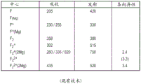
Fig. 1 is a table showing some of the various possible F-centers in luminescent sapphire, along with their absorption wavelengths (in nm) and their emission wavelengths.
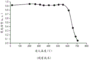
Fig. 2 is a graph showing how the fluorescence of a certain F-center in luminescent sapphire decreases during annealing above 600 ℃.
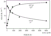
Fig. 3 is a graph showing how the absorption (and creation) of certain F-centers in luminescent sapphire increases over time during annealing at 500 ℃.
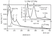
FIG. 4 is a graph showing the absorption of various F-centers in luminescent sapphire over a range of wavelengths, with the graph being magnified for wavelengths between 300 and 700 nm.
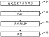
Fig. 5 is a flow chart of various steps for forming a dcLED with luminescent sapphire in accordance with a first embodiment of the present invention.
Fig. 6 is a cross-sectional view of a flip chip LED die having a coating of a luminescent sapphire mixture over the top of the LED die in accordance with a first embodiment of the invention.
Fig. 7 illustrates how the optical properties of the luminescent sapphire of fig. 6, after integration with an LED, can be changed to color shift the emission of the LED into a target color zone.
Fig. 8 is a cross-sectional view of a flip chip LED die with a pre-formed luminescent sapphire tile attached over the top of the LED die in accordance with a second embodiment of the present invention.
Fig. 9 is a flow chart of various steps for forming a dcLED with luminescent sapphire in accordance with a second embodiment of the present invention.
Fig. 10 is a cross-sectional view of a flip-chip LED die having its epitaxial layers grown over a light-emitting sapphire growth substrate in accordance with a third embodiment of the present invention.
Fig. 11 is a flow chart of various steps for forming a dcLED with luminescent sapphire in accordance with a third embodiment of the present invention.
Identical or similar elements are marked with the same reference numerals.
Detailed Description
Description of luminescent sapphire
Sapphire refers herein to alumina corundum in single crystal form. The main chemical composition being Al2O3. Sapphire may contain other elements as dopants and impurities, but is still considered sapphire. Single crystals of sapphire are typically grown using a variation of the Czochralski process.
As used herein, the term luminescent sapphire refers to a luminescent sapphire exhibiting an optical property corresponding to at least F thereof as described below2-luminescent sapphire with a shaped centre.
The F-shaped center is the color center of the luminescent sapphire. F-like centers are defined herein as the different chemical variants of a single vacancy of oxygen inside the sapphire lattice. Such oxygen vacancies are typically created by using a highly reducing atmosphere during sapphire crystal growth or subsequent annealing. Sapphire containing a high concentration of F-shaped centers is commonly referred to as Al2O3C or TCR sapphire (thermochemically reduced).
The most common variations of the F-shaped center are the following:
the F center is an oxygen vacancy trapping two electrons.
·F+The center is an oxygen vacancy that traps one electron.
The F (Mg) centre is the F centre around which one or several Mg cations are present.
·F+(Mg) centre is F with one or several Mg cations present around it+A center.
The presence of Mg cations around the F-like center results in shifts in absorption and emission.
The above identified centers are mainly identified by their optical absorption and luminescence emission as reported in the table of fig. 1. FIG. 1 identifies the known F-shapes and F in luminescent sapphire2-optical signature (signature) of the shape centre.
We will F2The shape center is defined as the different combination of two aggregated F-shaped centers. F2Well-reported variations of the centroid are the following:
·F2the center is a cluster of two F centers.
·F2 +The centre being an F+A cluster of centers and one F-center.
·F2 +(2Mg) center is one F around which there are two Mg cations2 +A cluster in the center.
·F2 2+The centre being two F+A cluster in the center.
·F2 2+(2Mg) center is the presence of two Mg cations surrounding itOne F of ion2 +A cluster in the center.
Some F2The shape center emits light (emission) in the visible spectrum (including green) and is therefore most relevant for the present invention.
The positioning of the oxygen vacancies with respect to each other is identified by the anisotropy of the optical absorption bands shown in fig. 1. Around F2The presence of Mg cations in the formal center leads to shifts in absorption and emission. In addition, each F2Different combinations of the shape centers may be present in the sapphire and will create slightly different optical characteristics of the sapphire.
Thermal processing of sapphire is used to create luminescent sapphire. This heat treatment is called sapphire activation. The process creates an aggregation of F-shaped centers to form F2-a centroid to thereby create a luminescent sapphire for use in the present invention.
Optical processing is used to tune the emission of the luminescent sapphire. This is called sapphire conditioning (conditioning). The process modifies the difference F2-concentration of the tabular center.
Thus, the various embodiments of dcleds using light emitting sapphire described below can be tuned to emit a wide variety of colors with suitable sapphire activation and adjustment.
Thermally activated F in sapphire2Creation and destruction of the shape center. Fig. 2 is a graph of the temperature stability of 750nm emission (secondary light) of luminescent sapphire under 650nm laser stimulation (primary light). FIG. 2 shows F emitted at 750nm2-shaped centre (see fig. 1, wherein F2 +(2Mg) emission with 750nm centers) rapidly decreases after annealing above about 600 ℃. Although the particular fluorescence and stimulus wavelengths in fig. 2 are not generally used in LED embodiments, fig. 2 shows how high temperatures generally affect the optical properties of the luminescent sapphire.
FIG. 3 is a graph of absorption coefficients for the 2.87eV and 4.8eV bands versus isothermal annealing time at 773K (500 ℃). Both the 2.87eV and 4.8eV bands are shorter wavelengths than typically used in LEDs. FIG. 3 shows F2-shaped centreOf the concentration of (A) is increased during annealing at 500 ℃ with F2 2+The illustrated increase in absorption coefficient correlates. FIG. 3 also shows F+The absorption coefficient decreases with annealing time.
As shown in fig. 2 and 3, F2The destruction of the shaped centers starts at approximately 600 ℃ and its filling (deposition) can be increased by an extended annealing of the sapphire at 500 ℃. During annealing at 500 ℃, F+Center aggregation to form F2 2+A center. With increasing annealing time, F2 2+The absorption coefficient of the center increases, and F+The absorption coefficient of the center decreases. The absorption coefficient is related to the filling in of the associated center. Such a concentration step (using heat) is referred to herein as sapphire activation.
Fig. 2 and 3 are obtained from the following papers: photomhrism of vacancy-related defects in thermochemical reduced alpha-Al of Ramirez, R2O3Mg single crystals, Applied Physics Letters, AIP, 2005, 86, 081914; and optical properties of vaccariaes in thermochemical reduced Mg-jointed sapphire single crystals, Journal of Applied Physics, AIP, 2007, 101, 123520, both of which are incorporated herein by reference.
The effect of Mg is reported to help F2-aggregation of the shaped centers. Such sapphire is also known as Al2O3C and Mg. Sapphire can be grown using known methods to have Al2O3C and Mg.
F in sapphire2One of the reported properties of the-shaped centers is the photochromic conversion under sufficient photon radiation flux. It has been reported that blue absorption/green emission F can be reduced by excitation of luminescent sapphire by a high peak power laser at a wavelength of 440nm2 2+Concentration of (2Mg) centers and increase F2 +(2Mg) center (equation 1 below). This is an optical treatment of the sapphire, which further tunes its fluorescence properties. The concentration of the other centers is simultaneously changed so that the charge balance remains free from interference. It is also reported that,F2 2+The concentration of (2Mg) centers can be increased by exciting the luminescent sapphire with a high peak power laser at a wavelength of 330nm (equation 2).
F2Such tuning of the concentration of the centroid by optical processing is defined herein as sapphire adjustment.


The photochromic properties of sapphire are not limited to 440nm and 330nm excitation. May be employed preferably at F2-other wavelengths at the absorption band of the shape center. The underlying "2-photon absorption process" that controls photochromic properties is well described in the literature and need not be described herein.
In one embodiment, the sapphire is subjected to activation (thermal) and conditioning (optical) to absorb some of the blue primary light generated by the pn junction of the LED and emit green secondary light. The precise activation and adjustment depends on the peak wavelength of the primary light, the thickness/density of the sapphire, the target color point, and other factors. The activation and adjustment required to achieve the target color may be determined empirically for a particular application. A red phosphor may then be added on top of the LED to create white light.
FIG. 4 is for Al2O3C, Mg and Al2O3C for F, F+And F2 +Graph of absorption at the (2Mg) center versus wavelength. The inset is an enlarged view for the wavelength 300-700 nm. Curve 20 is for sapphire "bleached" with a 435nm laser (sapphire tuning), and curve 22 is for sapphire "as grown" or annealed. Fig. 4 is taken from the following paper: new aluminum oxide single crystals for volumetric Data Storage, Optical Data Storage 2003, Optical Data Storage, S.A. Akselrod, M.S. et alPIE,2003, 5069, 244-; and the fluorine oxidative systems for volumetric optical data storage and imaging applications of Akselrod, M.S. et al, both of which are incorporated herein by reference.
Of particular interest are the wavelength ranges of about 450-650nm, which generally include the blue to red range.
Although the properties, creation, and adjustment of luminescent sapphire are well known, the inventors are not aware of any integration of luminescent sapphire in an LED die for down-conversion.
The Conversion Efficiency (CE) is the luminous flux (lm) emitted by the LED per amount of primary source light (including down-converted light). CE is a good scale for the efficiency of secondary sources (luminescent materials) and their integration in LEDs. In the following embodiments, using luminescent sapphire as the down-converter, the CE of the resulting LED is improved compared to the CE of pcleds.
Example 1
In the first embodiment, the luminescent sapphire is used in the form of powder instead of or in addition to the phosphor powder. An example of this first embodiment is represented by fig. 5 and 6.
As a preliminary matter, bulk luminescent sapphire (Al) was grown using conventional techniques2O3C, Mg or Al2O3C depending on the wavelength of interest) and activates and adjusts the sapphire, as described above and in accordance with known techniques, to have the desired light absorption and emission properties for a particular application (e.g., LED die and target color). Empirical testing may be performed to achieve the target absorption and emission properties. The target absorption wavelength will be the peak wavelength emission of the actual LED pn junction (active layer) used and will typically be in the visible blue range of wavelengths. In one embodiment, the emission of luminescent sapphire is green when excited with blue LED light (energize). Thus, adding a red phosphor layer will create warm white light.
In step 24 of fig. 5, the luminescent sapphire crystals are subjected to a grinding process and screened to a desired range of particle sizes. An acceptable range for the particle size distribution D50 is 10 to 50 μm. The particle size distribution D50 is also known as the median diameter of the particle size distribution and is the value of the particle diameter at 50% in the cumulative distribution.
In step 26, luminescent sapphire powder is injected into a transparent matrix (such as silicone) with appropriate and conventional additives and uniformly mixed. The additives selected depend on the application and may include phosphor powders, dispersants, and the like.
In step 28, the mixture is integrated into the LED so that it can absorb the primary light and down-convert it to the desired secondary light. For example, the mixture may be integrated by laminating (e.g., forming a pre-formed sheet or tile and attaching it over the LED wafer or die), overmolding (e.g., placing the LED die mounted on the wafer into a separate mold recess filled with the mixture and then curing the mixture), or spraying the mixture over at least the top surface of the LED die. The result is a dcLED characterized by a certain color point. The dcLED may or may not include phosphor in a mixture or as a separate layer.
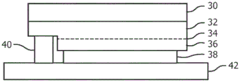
Fig. 6 is a cross-sectional view of one type of LED (flip chip) having a luminescent sapphire compound deposited as a luminescent sapphire layer 30 over the semiconductor surface of the LED and cured. Other types of LEDs may be used, such as vertical LEDs, lateral LEDs, and the like. In an example, an N-type layer 32 is epitaxially grown over a sapphire growth substrate (which is removed by laser lift-off), an active layer 34 is epitaxially grown over the N-type layer 32, and a P-type layer 36 is epitaxially grown over the active layer 34. Layers 34 and 36 are etched to expose N-type layer 32, and metal contacts 38 and 40 are deposited to electrically contact P-type layer 36 and N-type layer 32, respectively. The LED die is then mounted on a submount 42 or other substrate. The substrate 42 has metal pads that are directly bonded to the metal contacts 38 and 40, and the pads are ultimately electrically connected to a power source.
The exposed surface of the N-type layer 32 may be roughened to improve light extraction prior to deposition of the luminescent sapphire layer 30.
In prior art LEDs that only use phosphor for down conversion, if the target color point is not achieved, the LED is rejected or degraded to a lower quality LED. This increases the overall cost of LED production.
However, by using a layer of sapphire covering the N-type layer 32, the color point of the dcLED can be adjusted after the dcLED is activated and tested while bonded to the substrate 42 or while in wafer form and probed. The test may also be performed using an external excitation light source. The color point adjustment may be by sapphire adjustment (step 46), where the photochromic properties of the luminescent sapphire layer 30 are adjusted using a high peak power laser to create a color shift. Additional details are provided below. This post-integration adjustment increases the production yield (and thus reduces the production cost) of the dcLED and improves the color point control.
Finally, other additional optics such as a transparent dome lens (not shown) may be placed or molded over the dcLED to improve light extraction of the dcLED.
If the above process is performed on a wafer level, the LED die/substrate is then singulated.
One or more other layers between the LED semiconductor layers and the luminescent sapphire layer 30 may be present.
Practical example of embodiment 1
Having rich blue absorption/green emission F2 2+The (2Mg) centered luminescent sapphire was ground and sieved to a particle size in the range of 20 to 40 μm. The powder is mixed with silicone and red phosphor in such a ratio that the resulting dcLED color point is a warm white 3000K color temperature. The silicone employed is transparent and preferably has a refractive index greater than 1.50. The red phosphor used is, for example, the phosphor family (Ca, Sr) AlSiN3Eu or the phosphor group (Ba, Sr) Si5N8Eu. The paste silicone + luminescent sapphire powder + red phosphor are uniformly mixed to form the down-converter mixture (layer 30 in fig. 6). To create the desired warm white pcLED, the mixture is integrated with a primary blue source: for example, a blue emitting GaN-based LED die that emits a peak wavelength between 440 and 460 nm. These dies may be based on thin film flip chip technology and have InGaN/GaN p-N junction. Other types of LEDs may be used.
A well controlled volume of the mixture is dispensed over the die using any conventional deposition process normally used to dispense phosphor mixtures. The mixture is then cured by heat or UV. At this stage, some of the LED's color points may be outside the target zone for the 3000K LEDs.
In the example of fig. 7, the circle 50 represents the acceptable range of color points (target zone) that the final dcLED should exhibit. The u 'and v' axes represent coordinates in the CIE 1976 color system. Point 52 represents the color point of the LED(s) measured after the test following step 28 in fig. 5. The color point is then shifted to a point 54 within the circle 50 using a high power pulsed laser during the adjustment step 46 in fig. 5. The appropriate adjustment may be determined empirically. The testing and adjustment may be performed automatically by using a look-up table that cross-references the measured color points to the required adjustment for shifting the color emission into the target area circle 50. The required laser power and/or duration is then determined (again via a look-up table) and an adjustment is performed. The adjustment may be performed in an incremental manner, with a test being performed after each incremental step to ensure that there is no overcompensation.
If there is too much secondary light generated by the luminescent sapphire, the required adjustment can be obtained by reducing the down-conversion power of the luminescent sapphire. This may be achieved by reducing F in the luminescent sapphire during the conditioning step2 2+Concentration of (2Mg) centers. To this end, the luminescent sapphire may be exposed to a high peak power laser at a wavelength of 440nm for an empirically determined period of time. See equations 1 and 2 above.
Other adjustments may be used to create accurate color emission so that the LEDs do not need to be "thrown away".
Example 2
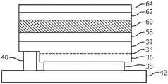
In a second embodiment shown in fig. 8 and 9, the luminescent sapphire is integrated as a pre-formed single crystal tile attached to the top surface of the primary light source.
In fig. 8, the primary light source LED is similar to that of fig. 6, with an N-type layer 32 epitaxially grown over the sapphire growth substrate, an active layer 34 epitaxially grown over the N-type layer 32, and a P-type layer 36 epitaxially grown over the active layer 34. Layers 34 and 36 are etched to expose N-type layer 32, and metal contacts 38 and 40 are deposited to electrically contact P-type layer 36 and N-type layer 32, respectively. The sapphire growth substrate is removed by laser lift-off and the exposed surface of the N-type layer 32 may then be roughened. The LED die is then mounted on a submount 42 or other substrate. The substrate 42 has metal pads that are directly bonded to the metal contacts 38 and 40, and the pads are ultimately electrically connected to a power source.
An adhesive layer 58, such as silicone, is deposited over the exposed N-type layer 32. The light emitting sapphire tiles 60 are then positioned and pressed onto the adhesive layer 58. An optional optical feature layer 62 may then be positioned or molded over tile 60, such as a filter layer or a textured layer for improved light extraction. An optional phosphor layer 64 (e.g., red phosphor in silicone binder) may then be deposited for additional color point adjustment. The laser exposure step for conditioning tile 60 may be performed before depositing layers 62 and 64. The laser exposure step may be performed on the tile 60 before or after attaching the tile 60 to the LED. All steps may be performed on a wafer level on a substrate wafer filled with an array of LED dies.
In another embodiment, the luminescent sapphire tile 60 comprises luminescent sapphire particles in a cured binder.
Fig. 9 identifies various steps for fabricating the device of fig. 8.
A flat luminescent sapphire crystal wafer is first formed (step 68) and then cut to have a size generally corresponding to the primary source LEDs (e.g., 1 mm)2) Of the tile (step 70). The tile 60 is then adjusted (step 72), using a laser, typically prior to singulation, so that it exhibits the desired F2Target concentration of the colour centre (see equations 1 and 2 above).
Tile 60 is then attached to the LED die using an adhesive layer (step 74).
At this stage, different options may be implemented:
a. no other phosphor is added to the device, whereby all down-conversion emission is performed by the luminescent sapphire tiles 60. The adjustment step may further be used to correct the color points, if necessary. In one example, by increasing F2 2+Filling in the (2Mg) center to increase green emission.
b. An optical signature layer 62, such as a dichroic filter, may be deposited (step 76) over the tiles 60 in order to control the emission (angle and spectrum).
c. One or more phosphors may be dispensed over tiles 60 (step 78) to form phosphor layer 64 in fig. 8. An optical feature layer 62, such as a dichroic filter, may optionally be deposited between the phosphor layer 64 and the tile 60. The adjustment step 80 may optionally be used to correct the LED color point while taking into account the phosphor contribution. For example, a warm white LED with a color temperature of 3000K may be manufactured by integrating a red-emitting phosphor layer 64 over the tile 60.
d. The same as version c, but with the phosphor layer integrated over the LED die first and then the light emitting sapphire tile 60 bonded over the phosphor layer. Optical feature layers and/or conditioning steps may also be applied prior to encapsulation of the device.
Example 3
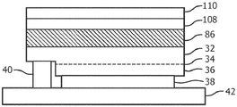
In the third embodiment, luminescent sapphire is used as a growth substrate on which LED semiconductor layers are epitaxially grown, as illustrated in fig. 10 and 11.
First, as shown in fig. 11, a sapphire single crystal is selected such that it contains a desired F-shaped center (step 84). The sapphire single crystal is prepared as a growth substrate 86 (fig. 10) by cutting and polishing to allow epitaxial growth thereon.
In step 88, a ill-nitride p-n junction (layers 32,34, 36) is grown on one side of the sapphire substrate 86. During this step, the temperature inside the growth reactor is maintained between 700 and 1100 ℃ under a reduced atmosphere for several hours. At such temperature and time, luminescence F of sapphire2The center of the shape is broken (see fig. 2). Due to the fact thatHere, it is meaningless to use luminescent sapphire as the growth substrate unless the center can be reactivated.
After epitaxial growth, the wafer is removed from the reactor. An anneal in the range of 500 to 600 c is then performed for several minutes to activate the P dopants in the P-type layer 36 of the ill-nitride junction (step 90). The annealing is performed in an atmosphere containing oxygen.
Additionally, at this stage of the process, the sapphire substrate 86 containing the F-shaped centers is activated (step 92) to create a luminescent sapphire. Physically, sapphire activation creates an aggregation of F-shaped centers to form F2-a shaped centre. The sapphire substrate 86 may be activated by annealing at a temperature in the range of 300-700 c (below the epitaxial growth temperature) or several anneals. For example, the sapphire substrate 86 may be activated by annealing the wafer at a temperature of 500 ℃ over several hours, as published in the literature. F2The concentration of the shape centers can be controlled by adjusting the annealing time and temperature. In addition, sapphire substrate 86 activation causes many types of F2-creation of a shape center. If only one particular class of F2Shape center is of interest for down-conversion, then F is expected2The concentration of the centroid can be obtained by applying a tuning (laser) step 94 to the sapphire substrate 86. For example, blue absorption/green emission F2 2+The concentration of (2Mg) centers can be increased by exciting the sapphire substrate 86 with a high peak power laser at a wavelength of 330 nm. The quality of such an adjustment can be determined, for example, by measuring the F of the luminescent sapphire2 2+The intensity of the fluorescence generated under excitation of the (2Mg) centre at 450nm (e.g. by an external source or by exciting an LED) is controlled.
Once the desired F is obtained2Target concentration of the centroid, the wafer can be returned to the normal manufacturing process for the LED, proceeding from the conventional wafer manufacturing step (ganged into step 96) to the die manufacturing step (ganged into step 98) to phosphor integration (step 100). During these subsequent steps, the temperature is kept below 600 ℃ and thus the activation of the sapphire substrate 86 is preservedAnd (4) remaining.
Optionally, more adjustment steps 102 and 104 may be added during the process to take advantage of the photochromic properties of luminescent sapphire. The adjusting step 102 may be performed after attaching the singulated dies to the substrate wafer in order to adjust the desired F for the actual primary light source efficiency and wavelength2Concentration of the centroid and reduction of the resulting v' dispersion of the LED fill-in. A further adjustment step 104 may be performed after the phosphor integration step 100 in order to tune the color point, as described in embodiment 1.
Optional features (step 106) may also be added to the LED die.
Fig. 10 shows an optical feature layer 108 and a phosphor layer 110, such as a dichroic filter layer and a red phosphor layer, for creating white light. The filter layer may reflect red light from the phosphor layer 110, but allow shorter wavelengths of light to pass through to avoid absorption of red light by the LED.
In addition to the various benefits described above, by performing all down-conversion from luminescent sapphire and not using phosphors, LEDs can be used in harsh environments for many years, such as in automotive headlamps. Phosphors are very sensitive to moisture and may eventually degrade in the headlamp environment.
The following references identify the state of the art in luminescent sapphire and illustrate what those skilled in the art will note. Such references demonstrate that one skilled in the art, after reading this disclosure, can make luminescent sapphire and perform the required activation and adjustments to achieve a target color point for a dcLED. Such references are incorporated herein by reference.
1. New aluminum oxide single crystals for volumetric optical data storage by Akselrod, M.S. et al,Optical Data Storage 2003, Optical data storage, SPIE,2003, 5069, 244-251
2. akselrod, M.S. et al, Fluorescent aluminum oxide crystals for volumetric optical data storage and imaging applications,J. Fluoresc.,2003, 13, 503-511
3.new Al from Akselrod, M, S, and Akselrod, A, E2O3:C,Mg crystals forradiophotoluminescent dosimetry and optical imaging,Radiat. Prot. Dosimetry,2006, 119, 218-221
4. Electrostemmescence in magnesium-doped Al, Ramirez, R. et Al2O3crystals,Radiation Effects and Defects in Solids,2001, 154, 295-299
5. Photom of vaccum-related defects reduced alpha-Al of Ramirez, R2O3:Mg single crystals,Applied Physics Letters, AIP,2005, 86, 081914
6. Ramirez, R. et al, Optical properties of vacarines in thermochemical reduced Mg-jointed sapphire single crystals,Journal of Applied Physics, AIP,2007, 101, 123520
7. sykora, G.et Al Novel Al2O3: C, Mg fluorescent nuclear track detector for passive neutron determination,Radiation Protection Dosimetry,2007, 126, 1-4
8. spectroscopic properties of novel fluorescent nuclear detectors for high and low LET charged particles by Sykora, G, et al,Radiation Measurements,2008, 43, 422 - 426
9. properties of novel fluorescent nuclear detectors for use in passive neutron determination by Sykora, G, et al,Radiation Measurements,2008, 43, 1017 - 1023
10. photocurable of photochromism and radiochromism transformed Al of Sykora, G.J. and Akselod, M.S2O3:C,Mg crystals used forfluorescent nuclear track detectors,Radiation Measurements,2010, 45, 631 -634
11. Tardio, M. et Al, High temperature separation characteristics of magnetic-doped alpha-Al2O3single crystals,Applied Physics Letters, AIP,2001, 79, 206-208
12. Tardio, M. et Al Electrical conductivity in magnesium-doped Al2O3crystals at modified temperatures,Radiation Effects and Defects in Solids,2001, 155, 409-413
13. photochromic effect in magnesium-doped alpha-Al of Tardio, M.et Al2O3single crystals,Applied Physics Letters, AIP,2003, 83, 881-883
14. Enhancing of electrical conductivity in alpha-Al sub 2 of Tardio, M. et Al]O[sub 3]crystals doped with magnesium,Journal of Applied Physics, AIP,2001, 90, 3942-3951
15. Tardio, M. et Al Electrical conductivity in unbound alpha-Al2O3crystals implanted with Mg ions,Nuclear Instruments and Methods in Physics Research Section B: Beam Interactions with Materials and Atoms,2008, 266,2932 – 2935。
while particular embodiments of the present invention have been shown and described, it will be obvious to those skilled in the art that changes and modifications may be made without departing from this invention in its broader aspects and, therefore, the appended claims are to encompass within their scope all such changes and modifications as fall within the true spirit and scope of this invention.
Claims (14)
1. A light emitting device comprising:
a Light Emitting Diode (LED) semiconductor layer including an N-type layer, an active layer emitting blue primary light, and a P-type layer; and
a luminescent sapphire affixed to the LED semiconductor layers, the LED semiconductor layers and the luminescent sapphire being part of an LED die, the luminescent sapphire comprising F resulting in a light emission band having a defined optical absorption and luminescence emission band2 2+(2Mg) central oxygen vacancy, said luminescent sapphire via F2 2+(2Mg) center absorbs a portion of the primary light and down-converts the primary light to emit green secondary light such that light from the LThe emission of the ED die includes a combination of at least the blue primary light and the green secondary light.
2. The device of claim 1, wherein the luminescent sapphire comprises luminescent sapphire particles combined with a binder to form a mixture, wherein the mixture is positioned to cover a light emission surface of the LED semiconductor layers.
3. The device of claim 2 wherein the mixture is laminated over the LED semiconductor layers.
4. The device of claim 2 wherein the mixture is molded over the LED semiconductor layers.
5. The device of claim 2, wherein the mixture is directly on one LED semiconductor layer.
6. The device of claim 1 wherein the luminescent sapphire comprises a preformed tile attached over the light emitting surface of the LED semiconductor layers.
7. The device of claim 6, wherein the tiles comprise a single crystal of luminescent sapphire.
8. The device of claim 6, wherein the tiles comprise luminescent sapphire particles in a binder.
9. The device of claim 6 wherein the tiles are directly attached to one LED semiconductor layer with an adhesive layer.
10. The device of claim 1, wherein the luminescent sapphire comprises a luminescent sapphire growth substrate on which the N-type layer, the active layer, and the P-type layer are epitaxially grown.
11. The device of claim 1 further comprising a phosphor layer overlying the LED semiconductor layers as part of the LED die such that light emission of the LED die comprises the blue primary light, the green secondary light from the luminescent sapphire, and light from the phosphor layer.
12. The device of claim 11, wherein the light from the phosphor layer comprises a red component.
13. A method, comprising:
providing a Light Emitting Diode (LED) die comprising LED semiconductor layers that generate blue primary light, and a luminescent sapphire layer that down-converts some of the blue primary light to green secondary light, such that light emitted by the LED die comprises a combination of at least the blue primary light and the green secondary light, the luminescent sapphire comprising F resulting in a defined optical absorption and luminescent emission band2 2+(2Mg) central oxygen vacancies; and
adjusting the luminescent sapphire layer in the LED die using a laser to adjust a characteristic of the green secondary light.
14. The method of claim 13, further comprising: activating the luminescent sapphire in the LED die by annealing the luminescent sapphire to increase its luminescent properties after the LED die is formed.
Applications Claiming Priority (5)
| Application Number | Priority Date | Filing Date | Title |
|---|---|---|---|
| US201361753175P | 2013-01-16 | 2013-01-16 | |
| US61/753175 | 2013-01-16 | ||
| US201361831244P | 2013-06-05 | 2013-06-05 | |
| US61/831244 | 2013-06-05 | ||
| CN201480005094.XA CN104904024A (en) | 2013-01-16 | 2014-01-02 | Led using luminescent sapphire as down-converter |
Related Parent Applications (1)
| Application Number | Title | Priority Date | Filing Date |
|---|---|---|---|
| CN201480005094.XA Division CN104904024A (en) | 2013-01-16 | 2014-01-02 | Led using luminescent sapphire as down-converter |
Publications (1)
| Publication Number | Publication Date |
|---|---|
| CN111697119A true CN111697119A (en) | 2020-09-22 |
Family
ID=49955454
Family Applications (2)
| Application Number | Title | Priority Date | Filing Date |
|---|---|---|---|
| CN201480005094.XA Pending CN104904024A (en) | 2013-01-16 | 2014-01-02 | Led using luminescent sapphire as down-converter |
| CN202010564496.0A Pending CN111697119A (en) | 2013-01-16 | 2014-01-02 | LED using luminescent sapphire as down-converter |
Family Applications Before (1)
| Application Number | Title | Priority Date | Filing Date |
|---|---|---|---|
| CN201480005094.XA Pending CN104904024A (en) | 2013-01-16 | 2014-01-02 | Led using luminescent sapphire as down-converter |
Country Status (7)
| Country | Link |
|---|---|
| US (2) | US20160027969A1 (en) |
| EP (1) | EP2946409B1 (en) |
| JP (1) | JP6622090B2 (en) |
| KR (1) | KR102145647B1 (en) |
| CN (2) | CN104904024A (en) |
| RU (1) | RU2686862C2 (en) |
| WO (1) | WO2014111822A1 (en) |
Families Citing this family (8)
| Publication number | Priority date | Publication date | Assignee | Title |
|---|---|---|---|---|
| US9528876B2 (en) * | 2014-09-29 | 2016-12-27 | Innovative Science Tools, Inc. | Solid state broad band near-infrared light source |
| US10217914B2 (en) * | 2015-05-27 | 2019-02-26 | Samsung Electronics Co., Ltd. | Semiconductor light emitting device |
| TWI644454B (en) | 2015-08-19 | 2018-12-11 | 佰鴻工業股份有限公司 | Light-emitting diode structure |
| JP2018022844A (en) | 2016-08-05 | 2018-02-08 | 日亜化学工業株式会社 | Light emitting apparatus and method of manufacturing the same |
| EP3309446A1 (en) * | 2016-10-17 | 2018-04-18 | Lumileds Holding B.V. | Light converting device with clamped light converter |
| EP3559996B1 (en) * | 2016-12-22 | 2021-03-24 | Lumileds LLC | Light emitting diodes with sensor segment for operational feedback |
| US10957825B2 (en) | 2017-09-25 | 2021-03-23 | Lg Innotek Co., Ltd. | Lighting module and lighting apparatus having thereof |
| JP7105884B2 (en) * | 2017-11-21 | 2022-07-25 | ルミレッズ リミテッド ライアビリティ カンパニー | Color error corrected segmented LED array |
Citations (5)
| Publication number | Priority date | Publication date | Assignee | Title |
|---|---|---|---|---|
| WO2001037351A1 (en) * | 1999-11-19 | 2001-05-25 | Cree Lighting Company | Multi color solid state led/laser |
| US20030218151A1 (en) * | 2001-12-04 | 2003-11-27 | Mark Akselrod | Aluminum oxide material for optical data storage |
| US20100045163A1 (en) * | 2006-11-17 | 2010-02-25 | Holger Winkler | Phosphor body containing ruby for white or colour-on-demand leds |
| WO2010079779A1 (en) * | 2009-01-07 | 2010-07-15 | 財団法人新産業創造研究機構 | Tunable laser oscillation oxide crystal preparation method |
| US20130234185A1 (en) * | 2012-03-06 | 2013-09-12 | Landauer, Inc. | Doped sapphire as substrate and light converter for light emitting diode |
Family Cites Families (16)
| Publication number | Priority date | Publication date | Assignee | Title |
|---|---|---|---|---|
| JPH11307813A (en) * | 1998-04-03 | 1999-11-05 | Hewlett Packard Co <Hp> | Light emitting device, its manufacture, and display |
| JP4151284B2 (en) * | 2001-03-05 | 2008-09-17 | 日亜化学工業株式会社 | Nitride semiconductor light-emitting element, light-emitting device, and manufacturing method thereof |
| RU2202843C2 (en) * | 2001-04-27 | 2003-04-20 | Институт проблем химической физики РАН | Semiconductor adjustable-color electroluminescent light source |
| JP2002344021A (en) * | 2001-05-16 | 2002-11-29 | Nichia Chem Ind Ltd | Light-emitting device |
| JP2004253743A (en) * | 2003-02-21 | 2004-09-09 | Nichia Chem Ind Ltd | Light emitting device using substrate containing activator |
| JP2004363149A (en) * | 2003-06-02 | 2004-12-24 | Matsushita Electric Ind Co Ltd | Light emitting element and its manufacturing method, and phosphor substrate and its manufacturing method |
| WO2006001316A1 (en) * | 2004-06-24 | 2006-01-05 | Ube Industries, Ltd. | White light emitting diode device |
| US8080828B2 (en) * | 2006-06-09 | 2011-12-20 | Philips Lumileds Lighting Company, Llc | Low profile side emitting LED with window layer and phosphor layer |
| CN100490196C (en) * | 2006-06-12 | 2009-05-20 | 武东星 | Solid luminous element of high light emission |
| EP2415847B1 (en) * | 2009-04-01 | 2014-12-31 | Hiroshima University | Method for producing aluminium oxide phosphor |
| TWI487141B (en) * | 2009-07-15 | 2015-06-01 | Advanced Optoelectronic Tech | Semiconductor optoelectronic structure of increased light extraction efficiency and fabricated thereof |
| DE102010005169A1 (en) | 2009-12-21 | 2011-06-22 | OSRAM Opto Semiconductors GmbH, 93055 | Radiation-emitting semiconductor component |
| KR102109668B1 (en) | 2010-04-08 | 2020-05-12 | 니치아 카가쿠 고교 가부시키가이샤 | Light-emitting device and process for production thereof |
| CN101834253A (en) * | 2010-05-06 | 2010-09-15 | 上海大学 | Zinc oxide laminate electrode gallium nitride-based high-power light-emitting diode and preparation method thereof |
| CN102157655B (en) * | 2011-02-28 | 2013-01-02 | 浙江大学 | Strontium titanate/P-type silicon heterojunction-based electroluminescent device and preparation method thereof |
| JP5739203B2 (en) * | 2011-03-24 | 2015-06-24 | 国立大学法人宇都宮大学 | Method for producing aluminum oxide phosphor |
-
2014
- 2014-01-02 EP EP14700314.9A patent/EP2946409B1/en active Active
- 2014-01-02 WO PCT/IB2014/058016 patent/WO2014111822A1/en active Application Filing
- 2014-01-02 KR KR1020157021999A patent/KR102145647B1/en active IP Right Grant
- 2014-01-02 JP JP2015552166A patent/JP6622090B2/en active Active
- 2014-01-02 US US14/761,115 patent/US20160027969A1/en not_active Abandoned
- 2014-01-02 RU RU2015134352A patent/RU2686862C2/en active
- 2014-01-02 CN CN201480005094.XA patent/CN104904024A/en active Pending
- 2014-01-02 CN CN202010564496.0A patent/CN111697119A/en active Pending
-
2016
- 2016-05-09 US US15/150,020 patent/US10181551B2/en active Active
Patent Citations (6)
| Publication number | Priority date | Publication date | Assignee | Title |
|---|---|---|---|---|
| WO2001037351A1 (en) * | 1999-11-19 | 2001-05-25 | Cree Lighting Company | Multi color solid state led/laser |
| US20040183088A1 (en) * | 1999-11-19 | 2004-09-23 | Nitres, Inc. | Multi element, multi color solid state LED/laser |
| US20030218151A1 (en) * | 2001-12-04 | 2003-11-27 | Mark Akselrod | Aluminum oxide material for optical data storage |
| US20100045163A1 (en) * | 2006-11-17 | 2010-02-25 | Holger Winkler | Phosphor body containing ruby for white or colour-on-demand leds |
| WO2010079779A1 (en) * | 2009-01-07 | 2010-07-15 | 財団法人新産業創造研究機構 | Tunable laser oscillation oxide crystal preparation method |
| US20130234185A1 (en) * | 2012-03-06 | 2013-09-12 | Landauer, Inc. | Doped sapphire as substrate and light converter for light emitting diode |
Non-Patent Citations (1)
| Title |
|---|
| SUBRATA SANYAL ET AL: "Anisotropy of optical absorption and fluorescence in Al2O3:C,Mg crystals" * |
Also Published As
| Publication number | Publication date |
|---|---|
| KR102145647B1 (en) | 2020-08-19 |
| RU2686862C2 (en) | 2019-05-06 |
| EP2946409B1 (en) | 2019-12-18 |
| US10181551B2 (en) | 2019-01-15 |
| KR20150110611A (en) | 2015-10-02 |
| US20160027969A1 (en) | 2016-01-28 |
| EP2946409A1 (en) | 2015-11-25 |
| JP2016508294A (en) | 2016-03-17 |
| WO2014111822A1 (en) | 2014-07-24 |
| JP6622090B2 (en) | 2019-12-18 |
| CN104904024A (en) | 2015-09-09 |
| RU2015134352A (en) | 2017-02-21 |
| US20160254420A1 (en) | 2016-09-01 |
Similar Documents
| Publication | Publication Date | Title |
|---|---|---|
| US10181551B2 (en) | LED using luminescent sapphire as down-converter | |
| US7446343B2 (en) | Phosphor converted light emitting device | |
| US7521862B2 (en) | Light emitting device including luminescent ceramic and light-scattering material | |
| JP5389029B2 (en) | Light source including a reflective wavelength conversion layer | |
| JP5951180B2 (en) | Emitter package with saturation conversion material | |
| JP2010514189A (en) | Multi-particle luminescent ceramics for light emitting devices | |
| WO2007080555A1 (en) | Phosphor converted light emitting device | |
| US11742463B2 (en) | Wavelength converted light emitting device | |
| JP5286639B2 (en) | Phosphor mixture, light emitting device, image display device, and illumination device | |
| US10312417B2 (en) | Wavelength converted light emitting device | |
| JP5652426B2 (en) | Phosphor mixture, light emitting device, image display device, and illumination device |
Legal Events
| Date | Code | Title | Description |
|---|---|---|---|
| PB01 | Publication | ||
| PB01 | Publication | ||
| SE01 | Entry into force of request for substantive examination | ||
| SE01 | Entry into force of request for substantive examination | ||
| WD01 | Invention patent application deemed withdrawn after publication |
Application publication date: 20200922 |
|
| WD01 | Invention patent application deemed withdrawn after publication |