CN111640528B - Anisotropic conductive film and connection structure - Google Patents
Anisotropic conductive film and connection structure Download PDFInfo
- Publication number
- CN111640528B CN111640528B CN202010304367.8A CN202010304367A CN111640528B CN 111640528 B CN111640528 B CN 111640528B CN 202010304367 A CN202010304367 A CN 202010304367A CN 111640528 B CN111640528 B CN 111640528B
- Authority
- CN
- China
- Prior art keywords
- axis
- conductive
- conductive particles
- particle
- anisotropic conductive
- Prior art date
- Legal status (The legal status is an assumption and is not a legal conclusion. Google has not performed a legal analysis and makes no representation as to the accuracy of the status listed.)
- Active
Links
Images


Classifications
-
- H—ELECTRICITY
- H01—ELECTRIC ELEMENTS
- H01L—SEMICONDUCTOR DEVICES NOT COVERED BY CLASS H10
- H01L24/00—Arrangements for connecting or disconnecting semiconductor or solid-state bodies; Methods or apparatus related thereto
- H01L24/01—Means for bonding being attached to, or being formed on, the surface to be connected, e.g. chip-to-package, die-attach, "first-level" interconnects; Manufacturing methods related thereto
- H01L24/26—Layer connectors, e.g. plate connectors, solder or adhesive layers; Manufacturing methods related thereto
- H01L24/28—Structure, shape, material or disposition of the layer connectors prior to the connecting process
- H01L24/29—Structure, shape, material or disposition of the layer connectors prior to the connecting process of an individual layer connector
-
- H—ELECTRICITY
- H01—ELECTRIC ELEMENTS
- H01B—CABLES; CONDUCTORS; INSULATORS; SELECTION OF MATERIALS FOR THEIR CONDUCTIVE, INSULATING OR DIELECTRIC PROPERTIES
- H01B5/00—Non-insulated conductors or conductive bodies characterised by their form
- H01B5/16—Non-insulated conductors or conductive bodies characterised by their form comprising conductive material in insulating or poorly conductive material, e.g. conductive rubber
-
- C—CHEMISTRY; METALLURGY
- C09—DYES; PAINTS; POLISHES; NATURAL RESINS; ADHESIVES; COMPOSITIONS NOT OTHERWISE PROVIDED FOR; APPLICATIONS OF MATERIALS NOT OTHERWISE PROVIDED FOR
- C09J—ADHESIVES; NON-MECHANICAL ASPECTS OF ADHESIVE PROCESSES IN GENERAL; ADHESIVE PROCESSES NOT PROVIDED FOR ELSEWHERE; USE OF MATERIALS AS ADHESIVES
- C09J163/00—Adhesives based on epoxy resins; Adhesives based on derivatives of epoxy resins
-
- C—CHEMISTRY; METALLURGY
- C09—DYES; PAINTS; POLISHES; NATURAL RESINS; ADHESIVES; COMPOSITIONS NOT OTHERWISE PROVIDED FOR; APPLICATIONS OF MATERIALS NOT OTHERWISE PROVIDED FOR
- C09J—ADHESIVES; NON-MECHANICAL ASPECTS OF ADHESIVE PROCESSES IN GENERAL; ADHESIVE PROCESSES NOT PROVIDED FOR ELSEWHERE; USE OF MATERIALS AS ADHESIVES
- C09J7/00—Adhesives in the form of films or foils
- C09J7/10—Adhesives in the form of films or foils without carriers
-
- C—CHEMISTRY; METALLURGY
- C09—DYES; PAINTS; POLISHES; NATURAL RESINS; ADHESIVES; COMPOSITIONS NOT OTHERWISE PROVIDED FOR; APPLICATIONS OF MATERIALS NOT OTHERWISE PROVIDED FOR
- C09J—ADHESIVES; NON-MECHANICAL ASPECTS OF ADHESIVE PROCESSES IN GENERAL; ADHESIVE PROCESSES NOT PROVIDED FOR ELSEWHERE; USE OF MATERIALS AS ADHESIVES
- C09J7/00—Adhesives in the form of films or foils
- C09J7/30—Adhesives in the form of films or foils characterised by the adhesive composition
-
- C—CHEMISTRY; METALLURGY
- C09—DYES; PAINTS; POLISHES; NATURAL RESINS; ADHESIVES; COMPOSITIONS NOT OTHERWISE PROVIDED FOR; APPLICATIONS OF MATERIALS NOT OTHERWISE PROVIDED FOR
- C09J—ADHESIVES; NON-MECHANICAL ASPECTS OF ADHESIVE PROCESSES IN GENERAL; ADHESIVE PROCESSES NOT PROVIDED FOR ELSEWHERE; USE OF MATERIALS AS ADHESIVES
- C09J9/00—Adhesives characterised by their physical nature or the effects produced, e.g. glue sticks
- C09J9/02—Electrically-conducting adhesives
-
- H—ELECTRICITY
- H01—ELECTRIC ELEMENTS
- H01B—CABLES; CONDUCTORS; INSULATORS; SELECTION OF MATERIALS FOR THEIR CONDUCTIVE, INSULATING OR DIELECTRIC PROPERTIES
- H01B13/00—Apparatus or processes specially adapted for manufacturing conductors or cables
- H01B13/0026—Apparatus for manufacturing conducting or semi-conducting layers, e.g. deposition of metal
-
- H—ELECTRICITY
- H01—ELECTRIC ELEMENTS
- H01L—SEMICONDUCTOR DEVICES NOT COVERED BY CLASS H10
- H01L24/00—Arrangements for connecting or disconnecting semiconductor or solid-state bodies; Methods or apparatus related thereto
- H01L24/01—Means for bonding being attached to, or being formed on, the surface to be connected, e.g. chip-to-package, die-attach, "first-level" interconnects; Manufacturing methods related thereto
- H01L24/26—Layer connectors, e.g. plate connectors, solder or adhesive layers; Manufacturing methods related thereto
- H01L24/27—Manufacturing methods
-
- H—ELECTRICITY
- H01—ELECTRIC ELEMENTS
- H01L—SEMICONDUCTOR DEVICES NOT COVERED BY CLASS H10
- H01L24/00—Arrangements for connecting or disconnecting semiconductor or solid-state bodies; Methods or apparatus related thereto
- H01L24/80—Methods for connecting semiconductor or other solid state bodies using means for bonding being attached to, or being formed on, the surface to be connected
- H01L24/83—Methods for connecting semiconductor or other solid state bodies using means for bonding being attached to, or being formed on, the surface to be connected using a layer connector
-
- H—ELECTRICITY
- H01—ELECTRIC ELEMENTS
- H01R—ELECTRICALLY-CONDUCTIVE CONNECTIONS; STRUCTURAL ASSOCIATIONS OF A PLURALITY OF MUTUALLY-INSULATED ELECTRICAL CONNECTING ELEMENTS; COUPLING DEVICES; CURRENT COLLECTORS
- H01R11/00—Individual connecting elements providing two or more spaced connecting locations for conductive members which are, or may be, thereby interconnected, e.g. end pieces for wires or cables supported by the wire or cable and having means for facilitating electrical connection to some other wire, terminal, or conductive member, blocks of binding posts
- H01R11/01—Individual connecting elements providing two or more spaced connecting locations for conductive members which are, or may be, thereby interconnected, e.g. end pieces for wires or cables supported by the wire or cable and having means for facilitating electrical connection to some other wire, terminal, or conductive member, blocks of binding posts characterised by the form or arrangement of the conductive interconnection between the connecting locations
-
- H—ELECTRICITY
- H05—ELECTRIC TECHNIQUES NOT OTHERWISE PROVIDED FOR
- H05K—PRINTED CIRCUITS; CASINGS OR CONSTRUCTIONAL DETAILS OF ELECTRIC APPARATUS; MANUFACTURE OF ASSEMBLAGES OF ELECTRICAL COMPONENTS
- H05K3/00—Apparatus or processes for manufacturing printed circuits
- H05K3/30—Assembling printed circuits with electric components, e.g. with resistor
- H05K3/32—Assembling printed circuits with electric components, e.g. with resistor electrically connecting electric components or wires to printed circuits
- H05K3/321—Assembling printed circuits with electric components, e.g. with resistor electrically connecting electric components or wires to printed circuits by conductive adhesives
- H05K3/323—Assembling printed circuits with electric components, e.g. with resistor electrically connecting electric components or wires to printed circuits by conductive adhesives by applying an anisotropic conductive adhesive layer over an array of pads
-
- C—CHEMISTRY; METALLURGY
- C08—ORGANIC MACROMOLECULAR COMPOUNDS; THEIR PREPARATION OR CHEMICAL WORKING-UP; COMPOSITIONS BASED THEREON
- C08K—Use of inorganic or non-macromolecular organic substances as compounding ingredients
- C08K3/00—Use of inorganic substances as compounding ingredients
- C08K3/02—Elements
- C08K3/08—Metals
- C08K2003/0862—Nickel
-
- H—ELECTRICITY
- H01—ELECTRIC ELEMENTS
- H01L—SEMICONDUCTOR DEVICES NOT COVERED BY CLASS H10
- H01L2224/00—Indexing scheme for arrangements for connecting or disconnecting semiconductor or solid-state bodies and methods related thereto as covered by H01L24/00
- H01L2224/01—Means for bonding being attached to, or being formed on, the surface to be connected, e.g. chip-to-package, die-attach, "first-level" interconnects; Manufacturing methods related thereto
- H01L2224/26—Layer connectors, e.g. plate connectors, solder or adhesive layers; Manufacturing methods related thereto
- H01L2224/27—Manufacturing methods
- H01L2224/271—Manufacture and pre-treatment of the layer connector preform
- H01L2224/2712—Applying permanent coating
-
- H—ELECTRICITY
- H01—ELECTRIC ELEMENTS
- H01L—SEMICONDUCTOR DEVICES NOT COVERED BY CLASS H10
- H01L2224/00—Indexing scheme for arrangements for connecting or disconnecting semiconductor or solid-state bodies and methods related thereto as covered by H01L24/00
- H01L2224/01—Means for bonding being attached to, or being formed on, the surface to be connected, e.g. chip-to-package, die-attach, "first-level" interconnects; Manufacturing methods related thereto
- H01L2224/26—Layer connectors, e.g. plate connectors, solder or adhesive layers; Manufacturing methods related thereto
- H01L2224/27—Manufacturing methods
- H01L2224/274—Manufacturing methods by blanket deposition of the material of the layer connector
- H01L2224/2746—Plating
- H01L2224/27464—Electroless plating
-
- H—ELECTRICITY
- H01—ELECTRIC ELEMENTS
- H01L—SEMICONDUCTOR DEVICES NOT COVERED BY CLASS H10
- H01L2224/00—Indexing scheme for arrangements for connecting or disconnecting semiconductor or solid-state bodies and methods related thereto as covered by H01L24/00
- H01L2224/01—Means for bonding being attached to, or being formed on, the surface to be connected, e.g. chip-to-package, die-attach, "first-level" interconnects; Manufacturing methods related thereto
- H01L2224/26—Layer connectors, e.g. plate connectors, solder or adhesive layers; Manufacturing methods related thereto
- H01L2224/28—Structure, shape, material or disposition of the layer connectors prior to the connecting process
- H01L2224/29—Structure, shape, material or disposition of the layer connectors prior to the connecting process of an individual layer connector
- H01L2224/29001—Core members of the layer connector
- H01L2224/29099—Material
- H01L2224/29198—Material with a principal constituent of the material being a combination of two or more materials in the form of a matrix with a filler, i.e. being a hybrid material, e.g. segmented structures, foams
- H01L2224/29199—Material of the matrix
- H01L2224/2929—Material of the matrix with a principal constituent of the material being a polymer, e.g. polyester, phenolic based polymer, epoxy
-
- H—ELECTRICITY
- H01—ELECTRIC ELEMENTS
- H01L—SEMICONDUCTOR DEVICES NOT COVERED BY CLASS H10
- H01L2224/00—Indexing scheme for arrangements for connecting or disconnecting semiconductor or solid-state bodies and methods related thereto as covered by H01L24/00
- H01L2224/01—Means for bonding being attached to, or being formed on, the surface to be connected, e.g. chip-to-package, die-attach, "first-level" interconnects; Manufacturing methods related thereto
- H01L2224/26—Layer connectors, e.g. plate connectors, solder or adhesive layers; Manufacturing methods related thereto
- H01L2224/28—Structure, shape, material or disposition of the layer connectors prior to the connecting process
- H01L2224/29—Structure, shape, material or disposition of the layer connectors prior to the connecting process of an individual layer connector
- H01L2224/29001—Core members of the layer connector
- H01L2224/29099—Material
- H01L2224/29198—Material with a principal constituent of the material being a combination of two or more materials in the form of a matrix with a filler, i.e. being a hybrid material, e.g. segmented structures, foams
- H01L2224/29298—Fillers
- H01L2224/29299—Base material
- H01L2224/293—Base material with a principal constituent of the material being a metal or a metalloid, e.g. boron [B], silicon [Si], germanium [Ge], arsenic [As], antimony [Sb], tellurium [Te] and polonium [Po], and alloys thereof
- H01L2224/29338—Base material with a principal constituent of the material being a metal or a metalloid, e.g. boron [B], silicon [Si], germanium [Ge], arsenic [As], antimony [Sb], tellurium [Te] and polonium [Po], and alloys thereof the principal constituent melting at a temperature of greater than or equal to 950°C and less than 1550°C
- H01L2224/29339—Silver [Ag] as principal constituent
-
- H—ELECTRICITY
- H01—ELECTRIC ELEMENTS
- H01L—SEMICONDUCTOR DEVICES NOT COVERED BY CLASS H10
- H01L2224/00—Indexing scheme for arrangements for connecting or disconnecting semiconductor or solid-state bodies and methods related thereto as covered by H01L24/00
- H01L2224/01—Means for bonding being attached to, or being formed on, the surface to be connected, e.g. chip-to-package, die-attach, "first-level" interconnects; Manufacturing methods related thereto
- H01L2224/26—Layer connectors, e.g. plate connectors, solder or adhesive layers; Manufacturing methods related thereto
- H01L2224/28—Structure, shape, material or disposition of the layer connectors prior to the connecting process
- H01L2224/29—Structure, shape, material or disposition of the layer connectors prior to the connecting process of an individual layer connector
- H01L2224/29001—Core members of the layer connector
- H01L2224/29099—Material
- H01L2224/29198—Material with a principal constituent of the material being a combination of two or more materials in the form of a matrix with a filler, i.e. being a hybrid material, e.g. segmented structures, foams
- H01L2224/29298—Fillers
- H01L2224/29299—Base material
- H01L2224/293—Base material with a principal constituent of the material being a metal or a metalloid, e.g. boron [B], silicon [Si], germanium [Ge], arsenic [As], antimony [Sb], tellurium [Te] and polonium [Po], and alloys thereof
- H01L2224/29338—Base material with a principal constituent of the material being a metal or a metalloid, e.g. boron [B], silicon [Si], germanium [Ge], arsenic [As], antimony [Sb], tellurium [Te] and polonium [Po], and alloys thereof the principal constituent melting at a temperature of greater than or equal to 950°C and less than 1550°C
- H01L2224/29344—Gold [Au] as principal constituent
-
- H—ELECTRICITY
- H01—ELECTRIC ELEMENTS
- H01L—SEMICONDUCTOR DEVICES NOT COVERED BY CLASS H10
- H01L2224/00—Indexing scheme for arrangements for connecting or disconnecting semiconductor or solid-state bodies and methods related thereto as covered by H01L24/00
- H01L2224/01—Means for bonding being attached to, or being formed on, the surface to be connected, e.g. chip-to-package, die-attach, "first-level" interconnects; Manufacturing methods related thereto
- H01L2224/26—Layer connectors, e.g. plate connectors, solder or adhesive layers; Manufacturing methods related thereto
- H01L2224/28—Structure, shape, material or disposition of the layer connectors prior to the connecting process
- H01L2224/29—Structure, shape, material or disposition of the layer connectors prior to the connecting process of an individual layer connector
- H01L2224/29001—Core members of the layer connector
- H01L2224/29099—Material
- H01L2224/29198—Material with a principal constituent of the material being a combination of two or more materials in the form of a matrix with a filler, i.e. being a hybrid material, e.g. segmented structures, foams
- H01L2224/29298—Fillers
- H01L2224/29299—Base material
- H01L2224/293—Base material with a principal constituent of the material being a metal or a metalloid, e.g. boron [B], silicon [Si], germanium [Ge], arsenic [As], antimony [Sb], tellurium [Te] and polonium [Po], and alloys thereof
- H01L2224/29338—Base material with a principal constituent of the material being a metal or a metalloid, e.g. boron [B], silicon [Si], germanium [Ge], arsenic [As], antimony [Sb], tellurium [Te] and polonium [Po], and alloys thereof the principal constituent melting at a temperature of greater than or equal to 950°C and less than 1550°C
- H01L2224/29347—Copper [Cu] as principal constituent
-
- H—ELECTRICITY
- H01—ELECTRIC ELEMENTS
- H01L—SEMICONDUCTOR DEVICES NOT COVERED BY CLASS H10
- H01L2224/00—Indexing scheme for arrangements for connecting or disconnecting semiconductor or solid-state bodies and methods related thereto as covered by H01L24/00
- H01L2224/01—Means for bonding being attached to, or being formed on, the surface to be connected, e.g. chip-to-package, die-attach, "first-level" interconnects; Manufacturing methods related thereto
- H01L2224/26—Layer connectors, e.g. plate connectors, solder or adhesive layers; Manufacturing methods related thereto
- H01L2224/28—Structure, shape, material or disposition of the layer connectors prior to the connecting process
- H01L2224/29—Structure, shape, material or disposition of the layer connectors prior to the connecting process of an individual layer connector
- H01L2224/29001—Core members of the layer connector
- H01L2224/29099—Material
- H01L2224/29198—Material with a principal constituent of the material being a combination of two or more materials in the form of a matrix with a filler, i.e. being a hybrid material, e.g. segmented structures, foams
- H01L2224/29298—Fillers
- H01L2224/29299—Base material
- H01L2224/293—Base material with a principal constituent of the material being a metal or a metalloid, e.g. boron [B], silicon [Si], germanium [Ge], arsenic [As], antimony [Sb], tellurium [Te] and polonium [Po], and alloys thereof
- H01L2224/29338—Base material with a principal constituent of the material being a metal or a metalloid, e.g. boron [B], silicon [Si], germanium [Ge], arsenic [As], antimony [Sb], tellurium [Te] and polonium [Po], and alloys thereof the principal constituent melting at a temperature of greater than or equal to 950°C and less than 1550°C
- H01L2224/29355—Nickel [Ni] as principal constituent
-
- H—ELECTRICITY
- H01—ELECTRIC ELEMENTS
- H01L—SEMICONDUCTOR DEVICES NOT COVERED BY CLASS H10
- H01L2224/00—Indexing scheme for arrangements for connecting or disconnecting semiconductor or solid-state bodies and methods related thereto as covered by H01L24/00
- H01L2224/01—Means for bonding being attached to, or being formed on, the surface to be connected, e.g. chip-to-package, die-attach, "first-level" interconnects; Manufacturing methods related thereto
- H01L2224/26—Layer connectors, e.g. plate connectors, solder or adhesive layers; Manufacturing methods related thereto
- H01L2224/28—Structure, shape, material or disposition of the layer connectors prior to the connecting process
- H01L2224/29—Structure, shape, material or disposition of the layer connectors prior to the connecting process of an individual layer connector
- H01L2224/29001—Core members of the layer connector
- H01L2224/29099—Material
- H01L2224/29198—Material with a principal constituent of the material being a combination of two or more materials in the form of a matrix with a filler, i.e. being a hybrid material, e.g. segmented structures, foams
- H01L2224/29298—Fillers
- H01L2224/29299—Base material
- H01L2224/293—Base material with a principal constituent of the material being a metal or a metalloid, e.g. boron [B], silicon [Si], germanium [Ge], arsenic [As], antimony [Sb], tellurium [Te] and polonium [Po], and alloys thereof
- H01L2224/29338—Base material with a principal constituent of the material being a metal or a metalloid, e.g. boron [B], silicon [Si], germanium [Ge], arsenic [As], antimony [Sb], tellurium [Te] and polonium [Po], and alloys thereof the principal constituent melting at a temperature of greater than or equal to 950°C and less than 1550°C
- H01L2224/29357—Cobalt [Co] as principal constituent
-
- H—ELECTRICITY
- H01—ELECTRIC ELEMENTS
- H01L—SEMICONDUCTOR DEVICES NOT COVERED BY CLASS H10
- H01L2224/00—Indexing scheme for arrangements for connecting or disconnecting semiconductor or solid-state bodies and methods related thereto as covered by H01L24/00
- H01L2224/01—Means for bonding being attached to, or being formed on, the surface to be connected, e.g. chip-to-package, die-attach, "first-level" interconnects; Manufacturing methods related thereto
- H01L2224/26—Layer connectors, e.g. plate connectors, solder or adhesive layers; Manufacturing methods related thereto
- H01L2224/28—Structure, shape, material or disposition of the layer connectors prior to the connecting process
- H01L2224/29—Structure, shape, material or disposition of the layer connectors prior to the connecting process of an individual layer connector
- H01L2224/29001—Core members of the layer connector
- H01L2224/29099—Material
- H01L2224/29198—Material with a principal constituent of the material being a combination of two or more materials in the form of a matrix with a filler, i.e. being a hybrid material, e.g. segmented structures, foams
- H01L2224/29298—Fillers
- H01L2224/29299—Base material
- H01L2224/293—Base material with a principal constituent of the material being a metal or a metalloid, e.g. boron [B], silicon [Si], germanium [Ge], arsenic [As], antimony [Sb], tellurium [Te] and polonium [Po], and alloys thereof
- H01L2224/29363—Base material with a principal constituent of the material being a metal or a metalloid, e.g. boron [B], silicon [Si], germanium [Ge], arsenic [As], antimony [Sb], tellurium [Te] and polonium [Po], and alloys thereof the principal constituent melting at a temperature of greater than 1550°C
- H01L2224/29364—Palladium [Pd] as principal constituent
-
- H—ELECTRICITY
- H01—ELECTRIC ELEMENTS
- H01L—SEMICONDUCTOR DEVICES NOT COVERED BY CLASS H10
- H01L2224/00—Indexing scheme for arrangements for connecting or disconnecting semiconductor or solid-state bodies and methods related thereto as covered by H01L24/00
- H01L2224/01—Means for bonding being attached to, or being formed on, the surface to be connected, e.g. chip-to-package, die-attach, "first-level" interconnects; Manufacturing methods related thereto
- H01L2224/26—Layer connectors, e.g. plate connectors, solder or adhesive layers; Manufacturing methods related thereto
- H01L2224/28—Structure, shape, material or disposition of the layer connectors prior to the connecting process
- H01L2224/29—Structure, shape, material or disposition of the layer connectors prior to the connecting process of an individual layer connector
- H01L2224/29001—Core members of the layer connector
- H01L2224/29099—Material
- H01L2224/29198—Material with a principal constituent of the material being a combination of two or more materials in the form of a matrix with a filler, i.e. being a hybrid material, e.g. segmented structures, foams
- H01L2224/29298—Fillers
- H01L2224/29299—Base material
- H01L2224/29386—Base material with a principal constituent of the material being a non metallic, non metalloid inorganic material
- H01L2224/29387—Ceramics, e.g. crystalline carbides, nitrides or oxides
-
- H—ELECTRICITY
- H01—ELECTRIC ELEMENTS
- H01L—SEMICONDUCTOR DEVICES NOT COVERED BY CLASS H10
- H01L2224/00—Indexing scheme for arrangements for connecting or disconnecting semiconductor or solid-state bodies and methods related thereto as covered by H01L24/00
- H01L2224/01—Means for bonding being attached to, or being formed on, the surface to be connected, e.g. chip-to-package, die-attach, "first-level" interconnects; Manufacturing methods related thereto
- H01L2224/26—Layer connectors, e.g. plate connectors, solder or adhesive layers; Manufacturing methods related thereto
- H01L2224/28—Structure, shape, material or disposition of the layer connectors prior to the connecting process
- H01L2224/29—Structure, shape, material or disposition of the layer connectors prior to the connecting process of an individual layer connector
- H01L2224/29001—Core members of the layer connector
- H01L2224/29099—Material
- H01L2224/29198—Material with a principal constituent of the material being a combination of two or more materials in the form of a matrix with a filler, i.e. being a hybrid material, e.g. segmented structures, foams
- H01L2224/29298—Fillers
- H01L2224/29299—Base material
- H01L2224/2939—Base material with a principal constituent of the material being a polymer, e.g. polyester, phenolic based polymer, epoxy
-
- H—ELECTRICITY
- H01—ELECTRIC ELEMENTS
- H01L—SEMICONDUCTOR DEVICES NOT COVERED BY CLASS H10
- H01L2224/00—Indexing scheme for arrangements for connecting or disconnecting semiconductor or solid-state bodies and methods related thereto as covered by H01L24/00
- H01L2224/01—Means for bonding being attached to, or being formed on, the surface to be connected, e.g. chip-to-package, die-attach, "first-level" interconnects; Manufacturing methods related thereto
- H01L2224/26—Layer connectors, e.g. plate connectors, solder or adhesive layers; Manufacturing methods related thereto
- H01L2224/28—Structure, shape, material or disposition of the layer connectors prior to the connecting process
- H01L2224/29—Structure, shape, material or disposition of the layer connectors prior to the connecting process of an individual layer connector
- H01L2224/29001—Core members of the layer connector
- H01L2224/29099—Material
- H01L2224/29198—Material with a principal constituent of the material being a combination of two or more materials in the form of a matrix with a filler, i.e. being a hybrid material, e.g. segmented structures, foams
- H01L2224/29298—Fillers
- H01L2224/29399—Coating material
- H01L2224/294—Coating material with a principal constituent of the material being a metal or a metalloid, e.g. boron [B], silicon [Si], germanium [Ge], arsenic [As], antimony [Sb], tellurium [Te] and polonium [Po], and alloys thereof
- H01L2224/29438—Coating material with a principal constituent of the material being a metal or a metalloid, e.g. boron [B], silicon [Si], germanium [Ge], arsenic [As], antimony [Sb], tellurium [Te] and polonium [Po], and alloys thereof the principal constituent melting at a temperature of greater than or equal to 950°C and less than 1550°C
- H01L2224/29439—Silver [Ag] as principal constituent
-
- H—ELECTRICITY
- H01—ELECTRIC ELEMENTS
- H01L—SEMICONDUCTOR DEVICES NOT COVERED BY CLASS H10
- H01L2224/00—Indexing scheme for arrangements for connecting or disconnecting semiconductor or solid-state bodies and methods related thereto as covered by H01L24/00
- H01L2224/01—Means for bonding being attached to, or being formed on, the surface to be connected, e.g. chip-to-package, die-attach, "first-level" interconnects; Manufacturing methods related thereto
- H01L2224/26—Layer connectors, e.g. plate connectors, solder or adhesive layers; Manufacturing methods related thereto
- H01L2224/28—Structure, shape, material or disposition of the layer connectors prior to the connecting process
- H01L2224/29—Structure, shape, material or disposition of the layer connectors prior to the connecting process of an individual layer connector
- H01L2224/29001—Core members of the layer connector
- H01L2224/29099—Material
- H01L2224/29198—Material with a principal constituent of the material being a combination of two or more materials in the form of a matrix with a filler, i.e. being a hybrid material, e.g. segmented structures, foams
- H01L2224/29298—Fillers
- H01L2224/29399—Coating material
- H01L2224/294—Coating material with a principal constituent of the material being a metal or a metalloid, e.g. boron [B], silicon [Si], germanium [Ge], arsenic [As], antimony [Sb], tellurium [Te] and polonium [Po], and alloys thereof
- H01L2224/29438—Coating material with a principal constituent of the material being a metal or a metalloid, e.g. boron [B], silicon [Si], germanium [Ge], arsenic [As], antimony [Sb], tellurium [Te] and polonium [Po], and alloys thereof the principal constituent melting at a temperature of greater than or equal to 950°C and less than 1550°C
- H01L2224/29444—Gold [Au] as principal constituent
-
- H—ELECTRICITY
- H01—ELECTRIC ELEMENTS
- H01L—SEMICONDUCTOR DEVICES NOT COVERED BY CLASS H10
- H01L2224/00—Indexing scheme for arrangements for connecting or disconnecting semiconductor or solid-state bodies and methods related thereto as covered by H01L24/00
- H01L2224/01—Means for bonding being attached to, or being formed on, the surface to be connected, e.g. chip-to-package, die-attach, "first-level" interconnects; Manufacturing methods related thereto
- H01L2224/26—Layer connectors, e.g. plate connectors, solder or adhesive layers; Manufacturing methods related thereto
- H01L2224/28—Structure, shape, material or disposition of the layer connectors prior to the connecting process
- H01L2224/29—Structure, shape, material or disposition of the layer connectors prior to the connecting process of an individual layer connector
- H01L2224/29001—Core members of the layer connector
- H01L2224/29099—Material
- H01L2224/29198—Material with a principal constituent of the material being a combination of two or more materials in the form of a matrix with a filler, i.e. being a hybrid material, e.g. segmented structures, foams
- H01L2224/29298—Fillers
- H01L2224/29399—Coating material
- H01L2224/294—Coating material with a principal constituent of the material being a metal or a metalloid, e.g. boron [B], silicon [Si], germanium [Ge], arsenic [As], antimony [Sb], tellurium [Te] and polonium [Po], and alloys thereof
- H01L2224/29438—Coating material with a principal constituent of the material being a metal or a metalloid, e.g. boron [B], silicon [Si], germanium [Ge], arsenic [As], antimony [Sb], tellurium [Te] and polonium [Po], and alloys thereof the principal constituent melting at a temperature of greater than or equal to 950°C and less than 1550°C
- H01L2224/29447—Copper [Cu] as principal constituent
-
- H—ELECTRICITY
- H01—ELECTRIC ELEMENTS
- H01L—SEMICONDUCTOR DEVICES NOT COVERED BY CLASS H10
- H01L2224/00—Indexing scheme for arrangements for connecting or disconnecting semiconductor or solid-state bodies and methods related thereto as covered by H01L24/00
- H01L2224/01—Means for bonding being attached to, or being formed on, the surface to be connected, e.g. chip-to-package, die-attach, "first-level" interconnects; Manufacturing methods related thereto
- H01L2224/26—Layer connectors, e.g. plate connectors, solder or adhesive layers; Manufacturing methods related thereto
- H01L2224/28—Structure, shape, material or disposition of the layer connectors prior to the connecting process
- H01L2224/29—Structure, shape, material or disposition of the layer connectors prior to the connecting process of an individual layer connector
- H01L2224/29001—Core members of the layer connector
- H01L2224/29099—Material
- H01L2224/29198—Material with a principal constituent of the material being a combination of two or more materials in the form of a matrix with a filler, i.e. being a hybrid material, e.g. segmented structures, foams
- H01L2224/29298—Fillers
- H01L2224/29399—Coating material
- H01L2224/294—Coating material with a principal constituent of the material being a metal or a metalloid, e.g. boron [B], silicon [Si], germanium [Ge], arsenic [As], antimony [Sb], tellurium [Te] and polonium [Po], and alloys thereof
- H01L2224/29438—Coating material with a principal constituent of the material being a metal or a metalloid, e.g. boron [B], silicon [Si], germanium [Ge], arsenic [As], antimony [Sb], tellurium [Te] and polonium [Po], and alloys thereof the principal constituent melting at a temperature of greater than or equal to 950°C and less than 1550°C
- H01L2224/29455—Nickel [Ni] as principal constituent
-
- H—ELECTRICITY
- H01—ELECTRIC ELEMENTS
- H01L—SEMICONDUCTOR DEVICES NOT COVERED BY CLASS H10
- H01L2224/00—Indexing scheme for arrangements for connecting or disconnecting semiconductor or solid-state bodies and methods related thereto as covered by H01L24/00
- H01L2224/01—Means for bonding being attached to, or being formed on, the surface to be connected, e.g. chip-to-package, die-attach, "first-level" interconnects; Manufacturing methods related thereto
- H01L2224/26—Layer connectors, e.g. plate connectors, solder or adhesive layers; Manufacturing methods related thereto
- H01L2224/28—Structure, shape, material or disposition of the layer connectors prior to the connecting process
- H01L2224/29—Structure, shape, material or disposition of the layer connectors prior to the connecting process of an individual layer connector
- H01L2224/29001—Core members of the layer connector
- H01L2224/29099—Material
- H01L2224/29198—Material with a principal constituent of the material being a combination of two or more materials in the form of a matrix with a filler, i.e. being a hybrid material, e.g. segmented structures, foams
- H01L2224/29298—Fillers
- H01L2224/29399—Coating material
- H01L2224/294—Coating material with a principal constituent of the material being a metal or a metalloid, e.g. boron [B], silicon [Si], germanium [Ge], arsenic [As], antimony [Sb], tellurium [Te] and polonium [Po], and alloys thereof
- H01L2224/29438—Coating material with a principal constituent of the material being a metal or a metalloid, e.g. boron [B], silicon [Si], germanium [Ge], arsenic [As], antimony [Sb], tellurium [Te] and polonium [Po], and alloys thereof the principal constituent melting at a temperature of greater than or equal to 950°C and less than 1550°C
- H01L2224/29457—Cobalt [Co] as principal constituent
-
- H—ELECTRICITY
- H01—ELECTRIC ELEMENTS
- H01L—SEMICONDUCTOR DEVICES NOT COVERED BY CLASS H10
- H01L2224/00—Indexing scheme for arrangements for connecting or disconnecting semiconductor or solid-state bodies and methods related thereto as covered by H01L24/00
- H01L2224/01—Means for bonding being attached to, or being formed on, the surface to be connected, e.g. chip-to-package, die-attach, "first-level" interconnects; Manufacturing methods related thereto
- H01L2224/26—Layer connectors, e.g. plate connectors, solder or adhesive layers; Manufacturing methods related thereto
- H01L2224/28—Structure, shape, material or disposition of the layer connectors prior to the connecting process
- H01L2224/29—Structure, shape, material or disposition of the layer connectors prior to the connecting process of an individual layer connector
- H01L2224/29001—Core members of the layer connector
- H01L2224/29099—Material
- H01L2224/29198—Material with a principal constituent of the material being a combination of two or more materials in the form of a matrix with a filler, i.e. being a hybrid material, e.g. segmented structures, foams
- H01L2224/29298—Fillers
- H01L2224/29399—Coating material
- H01L2224/294—Coating material with a principal constituent of the material being a metal or a metalloid, e.g. boron [B], silicon [Si], germanium [Ge], arsenic [As], antimony [Sb], tellurium [Te] and polonium [Po], and alloys thereof
- H01L2224/29463—Coating material with a principal constituent of the material being a metal or a metalloid, e.g. boron [B], silicon [Si], germanium [Ge], arsenic [As], antimony [Sb], tellurium [Te] and polonium [Po], and alloys thereof the principal constituent melting at a temperature of greater than 1550°C
- H01L2224/29464—Palladium [Pd] as principal constituent
-
- H—ELECTRICITY
- H01—ELECTRIC ELEMENTS
- H01L—SEMICONDUCTOR DEVICES NOT COVERED BY CLASS H10
- H01L2224/00—Indexing scheme for arrangements for connecting or disconnecting semiconductor or solid-state bodies and methods related thereto as covered by H01L24/00
- H01L2224/01—Means for bonding being attached to, or being formed on, the surface to be connected, e.g. chip-to-package, die-attach, "first-level" interconnects; Manufacturing methods related thereto
- H01L2224/26—Layer connectors, e.g. plate connectors, solder or adhesive layers; Manufacturing methods related thereto
- H01L2224/28—Structure, shape, material or disposition of the layer connectors prior to the connecting process
- H01L2224/29—Structure, shape, material or disposition of the layer connectors prior to the connecting process of an individual layer connector
- H01L2224/29001—Core members of the layer connector
- H01L2224/29099—Material
- H01L2224/29198—Material with a principal constituent of the material being a combination of two or more materials in the form of a matrix with a filler, i.e. being a hybrid material, e.g. segmented structures, foams
- H01L2224/29298—Fillers
- H01L2224/29499—Shape or distribution of the fillers
-
- H—ELECTRICITY
- H01—ELECTRIC ELEMENTS
- H01L—SEMICONDUCTOR DEVICES NOT COVERED BY CLASS H10
- H01L2224/00—Indexing scheme for arrangements for connecting or disconnecting semiconductor or solid-state bodies and methods related thereto as covered by H01L24/00
- H01L2224/01—Means for bonding being attached to, or being formed on, the surface to be connected, e.g. chip-to-package, die-attach, "first-level" interconnects; Manufacturing methods related thereto
- H01L2224/26—Layer connectors, e.g. plate connectors, solder or adhesive layers; Manufacturing methods related thereto
- H01L2224/31—Structure, shape, material or disposition of the layer connectors after the connecting process
- H01L2224/32—Structure, shape, material or disposition of the layer connectors after the connecting process of an individual layer connector
- H01L2224/321—Disposition
- H01L2224/32135—Disposition the layer connector connecting between different semiconductor or solid-state bodies, i.e. chip-to-chip
- H01L2224/32145—Disposition the layer connector connecting between different semiconductor or solid-state bodies, i.e. chip-to-chip the bodies being stacked
-
- H—ELECTRICITY
- H01—ELECTRIC ELEMENTS
- H01L—SEMICONDUCTOR DEVICES NOT COVERED BY CLASS H10
- H01L2224/00—Indexing scheme for arrangements for connecting or disconnecting semiconductor or solid-state bodies and methods related thereto as covered by H01L24/00
- H01L2224/01—Means for bonding being attached to, or being formed on, the surface to be connected, e.g. chip-to-package, die-attach, "first-level" interconnects; Manufacturing methods related thereto
- H01L2224/26—Layer connectors, e.g. plate connectors, solder or adhesive layers; Manufacturing methods related thereto
- H01L2224/31—Structure, shape, material or disposition of the layer connectors after the connecting process
- H01L2224/32—Structure, shape, material or disposition of the layer connectors after the connecting process of an individual layer connector
- H01L2224/321—Disposition
- H01L2224/32151—Disposition the layer connector connecting between a semiconductor or solid-state body and an item not being a semiconductor or solid-state body, e.g. chip-to-substrate, chip-to-passive
- H01L2224/32221—Disposition the layer connector connecting between a semiconductor or solid-state body and an item not being a semiconductor or solid-state body, e.g. chip-to-substrate, chip-to-passive the body and the item being stacked
- H01L2224/32225—Disposition the layer connector connecting between a semiconductor or solid-state body and an item not being a semiconductor or solid-state body, e.g. chip-to-substrate, chip-to-passive the body and the item being stacked the item being non-metallic, e.g. insulating substrate with or without metallisation
-
- H—ELECTRICITY
- H01—ELECTRIC ELEMENTS
- H01L—SEMICONDUCTOR DEVICES NOT COVERED BY CLASS H10
- H01L2224/00—Indexing scheme for arrangements for connecting or disconnecting semiconductor or solid-state bodies and methods related thereto as covered by H01L24/00
- H01L2224/80—Methods for connecting semiconductor or other solid state bodies using means for bonding being attached to, or being formed on, the surface to be connected
- H01L2224/81—Methods for connecting semiconductor or other solid state bodies using means for bonding being attached to, or being formed on, the surface to be connected using a bump connector
- H01L2224/819—Methods for connecting semiconductor or other solid state bodies using means for bonding being attached to, or being formed on, the surface to be connected using a bump connector with the bump connector not providing any mechanical bonding
- H01L2224/81901—Pressing the bump connector against the bonding areas by means of another connector
- H01L2224/81903—Pressing the bump connector against the bonding areas by means of another connector by means of a layer connector
-
- H—ELECTRICITY
- H01—ELECTRIC ELEMENTS
- H01L—SEMICONDUCTOR DEVICES NOT COVERED BY CLASS H10
- H01L2224/00—Indexing scheme for arrangements for connecting or disconnecting semiconductor or solid-state bodies and methods related thereto as covered by H01L24/00
- H01L2224/80—Methods for connecting semiconductor or other solid state bodies using means for bonding being attached to, or being formed on, the surface to be connected
- H01L2224/83—Methods for connecting semiconductor or other solid state bodies using means for bonding being attached to, or being formed on, the surface to be connected using a layer connector
- H01L2224/838—Bonding techniques
- H01L2224/8385—Bonding techniques using a polymer adhesive, e.g. an adhesive based on silicone, epoxy, polyimide, polyester
- H01L2224/83851—Bonding techniques using a polymer adhesive, e.g. an adhesive based on silicone, epoxy, polyimide, polyester being an anisotropic conductive adhesive
-
- H—ELECTRICITY
- H01—ELECTRIC ELEMENTS
- H01L—SEMICONDUCTOR DEVICES NOT COVERED BY CLASS H10
- H01L2224/00—Indexing scheme for arrangements for connecting or disconnecting semiconductor or solid-state bodies and methods related thereto as covered by H01L24/00
- H01L2224/91—Methods for connecting semiconductor or solid state bodies including different methods provided for in two or more of groups H01L2224/80 - H01L2224/90
- H01L2224/92—Specific sequence of method steps
- H01L2224/921—Connecting a surface with connectors of different types
- H01L2224/9211—Parallel connecting processes
-
- H—ELECTRICITY
- H01—ELECTRIC ELEMENTS
- H01L—SEMICONDUCTOR DEVICES NOT COVERED BY CLASS H10
- H01L24/00—Arrangements for connecting or disconnecting semiconductor or solid-state bodies; Methods or apparatus related thereto
- H01L24/01—Means for bonding being attached to, or being formed on, the surface to be connected, e.g. chip-to-package, die-attach, "first-level" interconnects; Manufacturing methods related thereto
- H01L24/26—Layer connectors, e.g. plate connectors, solder or adhesive layers; Manufacturing methods related thereto
- H01L24/31—Structure, shape, material or disposition of the layer connectors after the connecting process
- H01L24/32—Structure, shape, material or disposition of the layer connectors after the connecting process of an individual layer connector
-
- H—ELECTRICITY
- H05—ELECTRIC TECHNIQUES NOT OTHERWISE PROVIDED FOR
- H05K—PRINTED CIRCUITS; CASINGS OR CONSTRUCTIONAL DETAILS OF ELECTRIC APPARATUS; MANUFACTURE OF ASSEMBLAGES OF ELECTRICAL COMPONENTS
- H05K2201/00—Indexing scheme relating to printed circuits covered by H05K1/00
- H05K2201/09—Shape and layout
- H05K2201/09818—Shape or layout details not covered by a single group of H05K2201/09009 - H05K2201/09809
- H05K2201/09945—Universal aspects, e.g. universal inner layers or via grid, or anisotropic interposer
Abstract
The anisotropic conductive film includes an insulating adhesive layer and conductive particles disposed on the insulating adhesive layer. The conductive particles have an arrangement in which 1 st axes arranged at a predetermined particle pitch are aligned at a predetermined axial pitch. The conductive particles are substantially spherical, and when the average particle diameter of the conductive particles is D, the conductive particle pitch in the 1 st axis is 1.5D or more, and the shaft pitch in the 1 st axis is 1.5D or more. The direction (lattice axis) of each side of a 3-angle formed by any conductive particle in the 1 st axis, the conductive particle adjacent to the conductive particle in the 1 st axis, and the conductive particle closest to the conductive particle in the 1 st axis adjacent to the 1 st axis is oblique to the film width direction of the anisotropic conductive film. According to the anisotropic conductive film, stable connection reliability can be obtained, and an increase in manufacturing cost associated with an increase in density of conductive particles can be suppressed.
Description
The application is a divisional application of the following invention patent applications:
the invention name is as follows: an anisotropic conductive film and a connection structure; application No.: 201680027723.8, respectively; application date: 2016, 5 months and 27 days.
Technical Field
The present invention relates to an anisotropic conductive film and a connection structure connected by the anisotropic conductive film.
Background
Anisotropic conductive films are widely used when electronic components such as IC chips are mounted on a substrate. In recent years, a higher density of wiring has been required in small electronic devices such as mobile phones and notebook computers, and as a method for making an anisotropic conductive film correspond to this higher density, a technique is known in which conductive particles are uniformly arranged in a lattice shape in an insulating adhesive layer of the anisotropic conductive film.
However, even if the conductive particles are uniformly arranged, there is a problem that the connection resistance varies. This is because the conductive particles located on the edges of the terminals flow out into the gaps between the terminals due to the melting of the insulating adhesive, and are less likely to be sandwiched between the upper and lower terminals. In order to solve this problem, it has been proposed to use the 1 st alignment direction of the conductive particles as the longitudinal direction of the anisotropic conductive film and to incline the 2 nd alignment direction intersecting the 1 st alignment direction by 5 ° to 15 ° with respect to the direction orthogonal to the longitudinal direction of the anisotropic conductive film (patent document 1).
Documents of the prior art
Patent document
Patent document 1: japanese patent No. 4887700.
Disclosure of Invention
Problems to be solved by the invention
However, if the size of the terminals of the electronic components connected by the anisotropic conductive film is further reduced, the number of conductive particles that can be captured by the terminals is further reduced, and there are cases where sufficient conduction reliability cannot be obtained in the anisotropic conductive film described in patent document 1. In particular, in the so-called cog (chip on glass) connection for connecting a control IC such as a liquid crystal screen to a transparent electrode on a glass substrate, there is a problem that the terminal size becomes smaller with the increase in the number of terminals of the liquid crystal screen and the miniaturization of an IC chip, and further, when the glass substrate for a display of a television is connected to the fog (film on glass) of a Flexible Printed circuit board (FPC), the connection terminals have a fine pitch, and the number of conductive particles that can be captured by the connection terminals increases, thereby improving the conduction reliability.
In order to increase the number of conductive particles that can be captured by the connection terminal, it is conceivable to further increase the density of the conductive particles in the anisotropic conductive film. However, if the density of the conductive particles in the anisotropic conductive film is increased, there is a problem that the production cost of the anisotropic conductive film becomes high.
Therefore, the present invention aims to obtain stable conduction reliability by using an anisotropic conductive film even in a fine-pitch FOG connection or COG connection and to suppress an increase in manufacturing cost associated with an increase in density of conductive particles.
Means for solving the problems
The inventors found the following points: when the anisotropic conductive film is provided with an array of conductive particles in which axes of conductive particles arranged at a predetermined pitch are aligned at a predetermined axial pitch, if the direction of each side of a 3-corner formed by three adjacent conductive particles is made to be oblique to the film width direction of the anisotropic conductive film, even if the alignment between the opposite terminals of the anisotropic conductive connection is shifted to narrow the effective mounting area, the conductive particles can be sufficiently captured by the terminals to improve conduction reliability, and if substantially spherical particles are used as the conductive particles, the anisotropic conductive film in which the conductive particles are accurately arranged in a desired lattice-like array can be easily manufactured, and the connection state after the anisotropic conductive connection can be accurately determined by the indentations of the conductive particles on the terminals; and changing the pitch of the conductive particles in the lattice axis and the pitch of the lattice axis according to the width of the terminal to be connected by anisotropic conductivity, thereby reducing the density of the conductive particles required for securing conduction reliability.
That is, the present invention provides an anisotropic conductive film comprising an insulating adhesive layer and conductive particles disposed on the insulating adhesive layer, having an arrangement of the conductive particles in which the 1 st axis in which the conductive particles are arranged at a predetermined inter-axis distance is aligned at a predetermined inter-axis distance,
the conductive particles are substantially spherical and have a shape of a sphere,
when the average particle diameter of the conductive particles is D, the conductive particle pitch L1 on the 1 st axis is 1.5D or more, the axial pitch L3 on the 1 st axis is 1.5D or more,
the directions of the sides of the 3-angle formed by the arbitrary conductive particle P0 on the 1 st axis, the conductive particle P1 adjacent to the conductive particle P0 in the 1 st axis, and the conductive particle P2 closest to the conductive particle P0 on the 1 st axis adjacent to the 1 st axis are oblique to the film width direction of the anisotropic conductive film.
In addition, the present invention provides a connection structure in which a 1 st electronic component and a 2 nd electronic component are anisotropically electrically connected by the anisotropic conductive film.
Effects of the invention
According to the anisotropic conductive film of the present invention, when the conductive particles are regularly aligned in the insulating adhesive layer, the direction of each side of the 3-sided polygon formed by the adjacent three conductive particles is oblique to the film width of the anisotropic conductive film, and therefore, even if misalignment occurs between the opposite terminals connected in the anisotropic conductive film and the effective mounting area becomes narrow, the conductive particles can be sufficiently captured by each terminal. In addition, even if the terminal and the anisotropic conductive film are bonded to each other, the conductive particles can be sufficiently captured by each terminal even if the terminal and the anisotropic conductive film are displaced in any direction. Further, when each of the terminals for anisotropic conductive connection is rectangular and the terminals are arranged at a constant interval in a constant direction, the number of the conductive particles existing in the rectangle is reduced in dispersion, and therefore the number of the conductive particles captured by the terminals can be stabilized.
Further, the 1 st axis axial pitch L3 can be adjusted to correspond to the width of the terminal pitch, and the 1 st axis axial pitch L3 and the 1 st axis conductive particle pitch L1 can be adjusted to ensure a required distance even for the 1 st axis closest conductive particle distance L2, so that the number density of the conductive particles can be adjusted to a number density required for ensuring the conduction reliability without excessively increasing the number density of the conductive particles.
Further, by making the conductive particles substantially spherical, the conductive particles can be arranged accurately in the lattice arrangement. Further, if the particle diameters are substantially uniform, the connection state after anisotropic conductive connection can be accurately determined by the state of indentation or compression of the conductive particles on the terminal, and it is possible to prevent an excessive pressing force from being locally applied to the IC chip or the like to be connected.
Therefore, according to the anisotropic conductive film of the present invention, the conduction reliability of a connection structure using the anisotropic conductive film can be improved, and the increase in the production cost of the anisotropic conductive film accompanying the increase in the density of the conductive particles can be suppressed.
Drawings
Fig. 1 is a view showing the arrangement of conductive particles in an anisotropic conductive film 1 of an example.
Fig. 2A is an explanatory view of a connection state in a case where substantially spherical conductive particles are connected.
Fig. 2B is an explanatory view of a connection state in a case where substantially spherical conductive particles are connected.
Fig. 2C is an explanatory view of a connection state in the case where columnar conductive particles are connected to each other in fig. 2C.
Fig. 2D is an explanatory view of a connection state in the case where conductive particles having uneven particle diameters are connected.
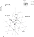
Fig. 3A is a modified example of the arrangement diagram of conductive particles in the anisotropic conductive film.
Fig. 3B is a modified example of the arrangement diagram of the conductive particles in the anisotropic conductive film.
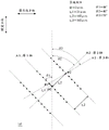
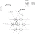
Fig. 4 is a view showing the arrangement of conductive particles in the anisotropic conductive film 1A of the embodiment.
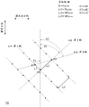
Fig. 5 is a view showing the arrangement of conductive particles in the anisotropic conductive film 1B of the example.
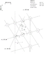
Fig. 6 is a layout view of conductive particles in the anisotropic conductive film 1C of the example.
Fig. 7 is a layout view of conductive particles in the anisotropic conductive film 1D of the example.
FIG. 8 is a view showing the arrangement of conductive particles in the anisotropic conductive film of the example.
FIG. 9 is a view showing the arrangement of conductive particles in the anisotropic conductive film of the example.
Fig. 10 is a layout view of conductive particles in the anisotropic conductive film of the example.
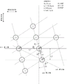
Fig. 11 is a layout view of conductive particles in the anisotropic conductive film 1E of the example.
Fig. 12 is a layout view of conductive particles in the anisotropic conductive film 1F of the example.
Fig. 13 is a layout view of conductive particles in an anisotropic conductive film 1G of a comparative example.
Fig. 14 is a layout view of conductive particles in an anisotropic conductive film of a comparative example.
Fig. 15 is a layout view of conductive particles in an anisotropic conductive film of a comparative example.
Fig. 16 is a view showing the arrangement of conductive particles in an anisotropic conductive film of a comparative example.
Fig. 17 is a layout view of conductive particles in an anisotropic conductive film of a comparative example.
Detailed Description
The present invention will be described in detail below with reference to the accompanying drawings. In the drawings, the same reference numerals denote the same or equivalent components.
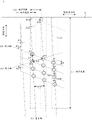
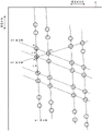
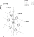
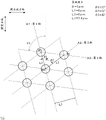
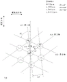
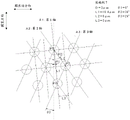
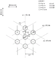
Fig. 1 is a diagram showing the arrangement of conductive particles P in an anisotropic conductive film 1 according to an embodiment of the present invention. The anisotropic conductive film 1 includes an insulating adhesive layer 2 and conductive particles P aligned and fixed in a lattice shape in the insulating adhesive layer 2. In the present invention, the ratio of the film length to the film width is usually 5000 or more. In fig. 1, the dotted line indicates the arrangement of the terminals 3 connected by the anisotropic conductive film 1.
The film length is preferably 5m or more, more preferably 10m or more, and further more preferably 30m or more in practical use. Although there is no particular upper limit, the cost of anisotropic connection is preferably 5000m or less, more preferably 1000m or less, and still more preferably 500m or less, in order to suppress the cost of anisotropic connection without excessively modifying the conventional connection device. The film width is not particularly limited, but is preferably 0.3mm or more so as to correspond not only to the terminal row region of a general electronic component but also to the terminal row region of a narrow frame, more preferably 0.5mm or more in terms of production of the anisotropic conductive film, and even more preferably 0.6mm or more in terms of production stability. Although there is no particular upper limit, it is generally 5mm or less. In applications such as stacking (stack) of ICs, a width larger than a wafer may be required, and therefore, about 30cm may be used.
The anisotropic conductive film may be connected by a connecting tape to be formed in a long shape as described above, or may be a wound body wound around a winding core.
< sphericity and particle size of conductive particle >)
The present invention has the main feature that the conductive particles P are substantially spherical. The term "substantially spherical" as used herein means that the sphericity is 70 to 100 as calculated by the following equation.
Sphericity { 1- (So-Si)/So } × 100
(wherein So is the area of a circumscribed circle of the conductive particle in a planar image of the conductive particle;
si is the area of an inscribed circle of the conductive particle in a planar image of the conductive particle)
In the calculation method, it is preferable that planar images of the conductive particles are captured at an in-plane view angle and a cross section of the anisotropic conductive film, an area of a circumscribed circle and an area of an inscribed circle of 100 or more (preferably 200 or more) arbitrary conductive particles in each planar image are measured, and an average value of the areas of the circumscribed circle and the inscribed circle is obtained as So and Si. In addition, the sphericity is preferably within the above range in both the surface view angle and the cross section. The difference between the sphericity of the cross-sectional view and the sphericity of the cross-sectional view is preferably within 20, more preferably within 10. The inspection in producing the anisotropic conductive film is mainly performed in a plane view, and the detailed quality determination after anisotropic connection is performed in both a plane view and a cross section, and therefore, the difference in sphericity is preferably small.
When the conductive particles P are spherical, for example, as described in japanese patent application laid-open No. 2014-60150, when an anisotropic conductive film in which conductive particles are arranged is manufactured by using a stamper, the conductive particles smoothly roll over the stamper, and thus the conductive particles can be filled in a predetermined position on the transfer mold with high accuracy. Therefore, the conductive particles can be accurately arranged so as to have a predetermined lattice axis arrangement. On the other hand, if the conductive particles are columnar, they are deviated in the rolling direction of the conductive particles, so that it is impossible to fill the transfer mold with the conductive particles with high accuracy, and even if they are spherical and flat, it is necessary to make the diameter of the concave portion of the transfer mold filled with the conductive particles considerably larger than the particle diameter of the conductive particles, so that it is difficult to accurately control the arrangement of the conductive particles.
In addition, in the connection structure in which the terminals of the 1 st electronic component and the terminals of the 2 nd electronic component are connected by the anisotropic conductive film by making the conductive particles P spherical and suppressing variation in particle diameter, the connection state can be accurately evaluated by the indentations of the conductive particles formed in the terminals. In particular, by suppressing the variation in the particle diameter of the conductive particles to 20% or less of the CV value (standard deviation/average), the evaluation of the connection state by indentation can be accurately performed. In addition, the entire conductive particles between the terminals are uniformly pressurized at the time of anisotropic conductive connection, and the pressing force can be prevented from being locally concentrated. On the other hand, if the particle size is excessively uniform, the terminal size will be a severe requirement, which may increase the cost of the anisotropic conductive film. On the other hand, if the CV value is within 20%, the connection state by indentation can be accurately confirmed not only for a large terminal size (FOG, etc.) but also for a small terminal size (COG, etc.).
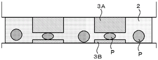
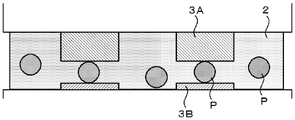
In any anisotropic connection, it is required that the connection state can be accurately evaluated by indentation of conductive particles, and the COG with a fine pitch is particularly preferable. That is, when the sphericity of the conductive particles before connection is high and the particle diameters are uniform, it is known that if the conductive particles P are flat circles between the terminals 3A and 3B facing each other in the cross section after connection as shown in fig. 2A, the facing terminals 3A and 3B are sufficiently crimped via the conductive particles P, and conduction can be reliably obtained, but if the press-in at the time of connection is insufficient and the conductive particles P are not crushed as shown in fig. 2B, the crimping is insufficient and conduction failure is caused. In such a case, the COG can determine whether or not the anisotropic connection is good by observing the COG from the glass side (transparent substrate side). That is, if the sheet is flat as shown in fig. 2A, the indentation is sufficiently developed, but if the press-fitting is insufficient as shown in fig. 2B, it is difficult to develop the sufficient indentation. Therefore, if the conductive particles are substantially spherical, the shape of the indentation is easily uniform, and thus it is easy to determine whether or not the pressure bonding by the indentation is good. In particular, in the case of the present invention in which the conductive particles are independently and separately arranged, this becomes remarkable. For this reason, it is also desirable that the conductive particles are substantially spherical.
Here, the variation in particle size can be calculated by an image-type particle size analyzer or the like. The particle size of the conductive particles, which are the raw material particles of the anisotropic conductive film, not disposed on the anisotropic conductive film can be determined using a wet flow particle size/shape analyzer FPIA-3000 (MALVERN corporation), as an example. When the conductive particles are disposed in the anisotropic conductive film, they can be obtained from a plane image or a cross-sectional image, as in the above-described sphericity.
In addition, the evaluation of the connection state by the crushing method of the conductive particles P can be particularly favorably performed when the metal-coated resin particles of the conductive layer are provided as the conductive particles P in the resin core.
In particular, in the case where a plurality of terminals are arranged, the connection state evaluation based on the collapse mode of the conductive particles P can be easily performed for each terminal because the collapse mode can be compared for each terminal. If the connection state between the adjacent terminals can be easily grasped, the productivity in the anisotropic connection process is also improved. This is because the conductive particles are preferably substantially spherical because they tend to be more conspicuously reflected.
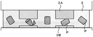
In contrast, when the conductive particles are not substantially spherical, the conductive particles have different crushing modes and different indentation modes depending on the contact direction with the terminal, and therefore, the connection state cannot be accurately evaluated based on the indentation. Further, in the case of the columnar shape, as shown in fig. 2C, the conductive particles P are easily crushed, and particles are generated which are crushed by concentrating the pressing force locally, and the connection state cannot be determined according to the degree of deformation. In addition, as shown in fig. 2D, even when there is an excessive variation in the particle size, the connection state cannot be determined according to the degree of deformation. Further, if there is a large variation in particle diameter, there is a fear that the sandwiching of the conductive particles between the opposing terminals is insufficient, and therefore, it is not preferable in terms of stabilizing the conduction reliability.
The conductive particles having a sphericity of 70 to 100 are preferably provided with a conductive layer on the resin core, from the viewpoint of ease of availability. The resin core can be produced by a known method such as suspension polymerization, emulsion polymerization, or seed polymerization, and has a certain degree of sphericity. By further performing an operation such as sieve classification or pulverization as appropriate, a resin core having a sphericity of at least a certain level can be obtained.
The resin core is preferably formed of particles made of a plastic material having excellent compression set, and can be formed of, for example, (meth) acrylate resin, polystyrene resin, styrene- (meth) propylene copolymer resin, urethane resin, epoxy resin, phenol resin, Acrylonitrile Styrene (AS) resin, benzoguanamine resin, divinylbenzene resin, styrene resin, polyester resin, or the like.
For example, when the resin core is formed of a (meth) acrylic resin, the (meth) acrylic resin is preferably a copolymer of a (meth) acrylic ester, a compound having a reactive double bond which can be copolymerized with the (meth) acrylic ester if necessary, and a bifunctional or polyfunctional monomer.
The resin core is preferably capable of being compressed to a hardness of about 70 to 80% after anisotropic bonding. Therefore, the resin core can be easily compressed and deformed according to the requirementsThe combination of the electronic components to be connected is variously selected. It is generally preferred that the compression hardness (K value) at 20% strain is 1500 to 4000N/mm2The relatively soft particles of (2) preferably have a compression hardness (K value) of 1500 to 4000/mm at 20% deformation even when the FPC and the FPC are anisotropically conductively connected (FOF) 2The relatively soft particles of (2). When the IC chip and the glass substrate are anisotropically and electrically connected to each other, the compression hardness (K value) at 20% deformation is preferably 3000 to 8000N/mm2Relatively hard particles. In the case of an electronic component in which an oxide film is formed on the surface of a wiring independently of the material, it may be preferable that the compression hardness (K value) at 20% strain be 8000N/mm2The above further hard particles. The upper limit of the hardness is limited because the material is a resin, and therefore, it is not particularly necessary to provide it.
Here, the compression hardness (K value) at 20% deformation means a load when the conductive particles are compressed by applying a load in one direction, and from the load when the conductive particles have a particle diameter 20% smaller than the original particle diameter, the particles become softer as the K value becomes smaller, as calculated by the following equation.

(wherein F represents a load at 20% compression deformation of the conductive particles
S: compressive displacement (mm)
R: radius (mm) of conductive particles).
Further, according to the above method for producing a resin core, the resin core may be produced as an aggregate (secondary particle). In this case, the resin core aggregated is pulverized. In the pulverization, it is preferable to disentangle aggregates of the resin cores aggregated in the drying of the solvent without deforming the particle shape. Such an operation can be performed by using an air-flow type micro-pulverization device. Examples of such a device include a bench-top laboratory JET MILL (Toho model ラボジェットミル) A-O JET MILL, a mini JET system (コジェットシステム) (both manufactured by SEISHIN corporation), and the like. Centrifugal recovery mechanisms may also be combined.
In 70 to 100 degrees of sphericity, as a method for obtaining a resin core having a relatively low degree of sphericity, an aggregate of resin particles having a wide particle size distribution (soot) is prepared, and the classification/pulverization operation is appropriately adjusted, whereby a resin core composed of an aggregate of a plurality of resin particles can be obtained. The height of the protrusions can be, for example, 10 to 500nm or 10% or less of the particle size.
Further, protrusions may be formed on the surface of the conductive particles. For example, the conductive particles described in japanese patent application laid-open No. 2015-8129 and the like can be used. By forming such a protrusion, the protective film provided on the terminal can be pierced at the time of anisotropic connection. The protrusions are preferably formed uniformly on the surfaces of the conductive particles, but in the step of filling the mold with the conductive particles in order to align the conductive particles in the step of producing the anisotropic conductive film, defects may be generated in a part of the protrusions.
The material of the conductive particles P may be, for example, metal particles such as nickel, cobalt, silver, copper, gold, palladium, or solder, in addition to the metal-coated resin particles. More than 2 kinds may be used in combination. Further, the conductive particles to be supplied to the production of the anisotropic conductive film may be formed as 2-order particles.
In the present invention, the particle diameter D of the conductive particle P means an average particle diameter. The particle diameter D of the conductive particles P is preferably 1 to 30 μm, more preferably 2.5 to 15 μm, from the viewpoint of stability in preventing short-circuiting and bonding between terminals to be connected. In the anisotropic conductive connection, although a protective film may be provided on a terminal sandwiching a conductive particle or a terminal surface may be uneven, when the conductive particle size is preferably 2.5 μm or more, and more preferably 3 μm or more, the conductive particle can be stably sandwiched by the terminal even in such a case.
< number density of conductive particles >)
The number density of the conductive particles P in the present invention can be adjusted to a suitable range for securing conduction reliability by changing the arrangement of the conductive particles P according to the terminal width or the terminal pitch of the connection target. Generally, in both the FOG connection and the COG connection, if 3 or more, preferably 10 or more, conductive particles can be trapped in a pair of opposing terminals, good conduction characteristics can be obtained.
For example, in the case of FOG connection in which the width of a terminal to be connected is 30 times or more the conductive particle diameter, the area of a portion where the opposing terminals overlap each other (effective connection area) is sufficient, and therefore, the number density of conductive particles is set to 7 to 25 particles/mm 2And connection can be performed. More specifically, the width of the terminal of the connection part is 0.2mm, the length of the terminal is 2mm or more, the gap between the terminals is 0.2mm (L/S is 1), the film width of the anisotropic conductive film is 2mm, and when the connection is performed with the film width, the density of the conductive particles can be reduced to 7 to 8 particles/mm2Degree of the disease. In this case, even if the film widths are not all connected, the film may be pressed with a tool having a length equal to or less than the film width. Since the pressed portion has an effective connection area, the length of the terminal to be connected is 2mm or less.
In the case where the terminal to be connected is long as described above but narrow (for example, FPC having a terminal width of 10 to 40 μm), in order to improve productivity of the anisotropic connection step, and when quick workability including an alignment step which is a step before connection is required, it is preferable that the number density of the conductive particles is 38 to 500 particles/mm2To allow for a reduction in the effective connection area caused by a shift in the alignment of the opposing terminals. The alignment deviation is preferably 150-500 pieces/mm in the state that the effective width of the terminal is narrowed to about 10 μm2。
On the other hand, in the FOG connection of a touch panel or the like, the length of the terminal may be shortened in order to narrow the frame, and for example, it is necessary to connect an FPC having a terminal width of 20 to 40 μm and a length of 0.7mm or less, preferably 0.5mm or less. In this case, the number density of the conductive particles is preferably 108 to 2000 particles/mm 2More preferably 500 to 2000 pieces/mm2。
Summarizing the above, the present invention relates to conductive particlesThe lower limit of the number density is determined by the terminal width or the terminal length, or the length of the connection (tool width), but if 7/mm2The above is preferable, if 38/mm2The above is more preferred, and 108/mm2It is still more preferable if the number of the above is 500/mm2In the above, the effective connection area can be reduced to some extent.
The number density of the conductive particles may be reduced as much as possible for each connection object, but since mass production does not tend to occur when the number of manufactured products is increased, the maximum number of the conductive particles per mm of the lower limit may be 500/mm which is the maximum number2The above anisotropic conductive film covers a variety having a lower limit less than that. Furthermore, if the manufacturing margin (margin) in mass production is added, about 20% can be added to 600 pieces/mm2As a lower limit value. This is because the effect of reducing the number of conductive particles described later may be effective in a mode of reducing the variety to be manufactured. Particularly, if the number density is 3000 pieces/mm2Preferably 2500 pieces/mm or less2Hereinafter, more preferably 2000 pieces/mm2Hereinafter, it is assumed that each terminal has a thickness of 5000 μm 2The terminal layout of the effective connection area described above has a sufficient inter-terminal distance (for example, if the conductive particle diameter is 5 μm or less, a distance of 20 μm or more, preferably 30 μm or more, and more preferably greater than 30 μm, or a distance of 4 times or more, preferably 6 times or more, and more preferably greater than 6 times the conductive particle diameter). In this case, since the conductive particles are independently arranged in the present invention, occurrence of short circuit can be greatly avoided, and the effect of reducing the total cost becomes more remarkable. As will be described later, the fine pitch and the normal pitch are distinguished at a boundary of 30 μm for convenience in the present invention, but with the diversification of portable image display devices in recent years, electronic components are also diversified. By setting the number density of the conductive particles in the present invention to a value that can cover a wide variety of types as described above, the present invention is in a form that has been further developed from anisotropic conductive films that have been widely used.
In the anisotropic conductive connection, it is preferable that the film width direction of the anisotropic conductive film 1 and the longitudinal direction of the terminal 3 are matched in order to facilitate the continuous film adhesion process to the electronic component before connection and to stably hold the conductive particles between the opposing terminals in both of the FOG connection and the COG connection. On the other hand, in both of the FOG connection and the COG connection, if the number density of the conductive particles is excessively increased, the production cost of the anisotropic conductive film increases, and the pressing force increases in the anisotropic conductive connection. When the number of terminals increases due to fine pitches, if the number of conductive particles captured by each terminal is too large, the pressing force of a conventional connection pressing device used for anisotropic conductive connection cannot be applied. On the other hand, there is a concern that cost increases when the apparatus is modified.
Therefore, in order to suppress application of excessive pressing force in FOG connection or COG connection, it is preferable that 50 or less, more preferably 40 or less, and still more preferably 20 or less conductive particles are trapped in 1 set of opposing terminals.
Although there are various terminal sizes in COG connection, if a terminal width of 10 μm and a terminal length of 50 μm are assumed as an example, the number density of the conductive particles is preferably 100000 particles/mm in order to suppress application of excessive pressing force2The number of particles is preferably 80000/mm2The following.
In the above manner, it is preferable that 1 set of opposing terminals trap preferably 3 to 50, more preferably 10 to 40 conductive particles, regardless of the size or area of the terminals. When the number density of the conductive particles is set so as to have such a trapping number, the FOG connection is preferably 40 to 3000 particles/mm when the terminal width is 20 to 40 μm and the terminal length is 500 to 2000 μm2Particularly preferably 50 to 2500 pieces/mm2. The above-described terminal length may also be considered as a length (i.e., a tool width) as an area of connection. Further, as an example of COG connection, it is preferable that the number of terminals is 4000 to 100000 pieces/mm when the terminal width is 5 to 50 μm and the terminal length is 30 to 300 μm 2Particularly preferably 5000 to 80000 pieces/mm2. By setting the number density of the conductive particles within this range, a pattern in which the conductive particles are arranged in accordance with the necessary minimum limit of the terminal width or the terminal length can be prepared. FOG and COG are used as descriptions of general anisotropic connection, and electronic components are not necessarily limited to FPC, IC chip, and glass substrate, and may be replaced by similar ones.
< arrangement of conductive particles >
In the present invention, the arrangement of the conductive particles P is such that the 1 st axis a1 in which the conductive particles P are arranged at the predetermined conductive particle pitch L1 is aligned at the predetermined axial pitch L3, and in the anisotropic conductive film 1 shown in fig. 1, the conductive particle pitch L1 and the axial pitch L3 of the 1 st axis a1 and the closest inter-particle distance L2 of the adjacent 1 st axis a1 are arranged in a lattice shape having a specific size with respect to the conductive particle diameter D as described below, and further, the lattice axes a1, a2, and A3 forming the main 3 directions of the lattice shape arrangement of the conductive particles P are obliquely crossed with the film width direction of the anisotropic conductive film.
By such skew, an effect of stabilizing the number of the conductive particles P captured by the terminal 3 can be expected. When the lattice axis (also referred to as an alignment axis) of the conductive particles P is parallel to the outer shape of the rectangular terminal 3, that is, parallel to the longitudinal direction or the short-side direction of the film, an extreme phenomenon occurs in which all or none of the conductive particles P are captured when the alignment of the conductive particles P is present at the end of the terminal 3. In order to avoid this, if the position adjustment is performed during the adhesion of the film, the manufacturing cost of the interconnector increases, such as the position determination of each of the terminals and the conductive particles in the film, as needed. To avoid this, it is critical that the number of terminal captures do not vary extremely at any location within the film. Therefore, it is desirable that the alignment axes a1, a2, and A3 of the conductive particles P are oblique to the film width direction (the longitudinal direction of the rectangular terminal in general anisotropic connection).
< conductive particle spacing L1>
When the average particle diameter of the conductive particles P is D, the conductive particle pitch L1 on the 1 st axis a1 is set to be 1.5D or more in terms of preventing short-circuiting between terminals arranged in the same component and stability of bonding between opposing terminals of the 1 st and 2 nd electronic components when the terminals of the 1 st electronic component and the terminals of the 2 nd electronic component are anisotropically conductively connected by the anisotropic conductive film 1.
The conductive particles P on the 1 st axis a1 may not be exactly aligned, but may be dispersed in a stripe-like line having a width sufficiently smaller than the inter-axis distance L3. The discrete tape widths are preferably less than 0.5 times the conductive particle diameter D in terms of the center-to-center distance of the conductive particles. This has the effect of stabilizing the trapping number of the conductive particles with respect to the terminal end portion as described above.
As described above, it is preferable that the film width direction of the anisotropic conductive film 1 is matched with the longitudinal direction of the terminal 3, and therefore, in the case of FOG connection, the length of the conductive particle pitch L1 in the 1 st axis a1 direction in the anisotropic conductive film 1 can be made substantially equal to the length Lr of the terminal 3 in the longitudinal direction (hereinafter, referred to as terminal length) at maximum. The terminal length Lr is usually 2000 μm or less. When 3 conductive particles are arranged so as to have a terminal length Lr2000 μm, the conductive particle pitch L1 is preferably set to less than 1000D, and is preferably 221D or less in particular from the viewpoint of stable conduction performance.
On the other hand, in the case of COG connection, the terminal length Lr is usually 200 μm or less, and the assumed terminal width Lq is set to 3 μm at minimum on the assumption of a shift in alignment between the opposing terminals. In this case, the length of the 1 st axis a1 on the terminal 3 may be set to be substantially equal to the terminal length Lr at maximum and 200 μm or less. In the case where 3 or more conductive particles are present, the conductive particle pitch L1 is preferably set to less than 100D, more preferably 22D or less in particular from the viewpoint of stable conduction performance, and still more preferably 10D or less from the viewpoint of visibility of the 1 st axis a 1.
Further, by setting the arrangement axis having the smallest pitch among the arrangement axes of the conductive particles as the 1 st axis a1, it is possible to define and design the arrangement pattern shown in fig. 12, 13, and the like described later so as to facilitate understanding of the characteristics of the particle arrangement.
The conductive particle pitch L1 of the 1 st axis a1 does not need to be strictly at equal intervals when the pitch is small. In this case, for example, as shown in fig. 3A, the 1 st axial pitch preferably includes regular repetitions of wide and narrow pitches L1a and L1 b. If the pitch is regularly narrowed in the same lattice axis, the number density of the conductive particles can be relatively increased in the portion where the terminal is present, and the number density of the conductive particles can be relatively decreased in the portion where the terminal is not present (such as the inter-bump gap). By doing so, the number of traps to the terminal is increased, and the risk of short-circuiting is easily avoided. The same applies to the pitch of the conductive particles in the 2 nd axis a2 and the 3 rd axis A3. In other words, the interval of the inter-axis distance of at least one lattice axis may be made regular.
< axle spacing L3>
If the discrete width of the conductive particles within 1 of the 1 st axes a1 is considered to be 0.5D, the inter-axial distance L3 of the 1 st axis a1 is more preferably greater than 2D. In the case of COG connection, it is preferable that 1 terminal intersects 3 or more alignment lines of the 1 st axis a1 in terms of stabilizing the number of captured conductive particles.
The upper limit of the axial distance L3 can be appropriately selected depending on the conductive particle distance L1 or the connection target. In the case of FOG connection, since the terminal length is sufficiently longer than the conductive particle diameter, it is possible to capture conductive particles sufficient to ensure conduction in a part of the arrangement line of one 1 st axis a1, and therefore the terminal width may be further reduced, preferably less than 200D, more preferably less than 80D.
On the other hand, if it is assumed that IC chips are stacked by TSVs or the like, the terminals correspond to solder joints of at least about 30 μm, and therefore 3 or more lines of arrangement of the 1 st axis a1 intersect there, and therefore the inter-axis distance L3 is preferably less than 10D, more preferably less than 4D.
< relationship between L1 and L3>
The arrangement of the conductive particles is designed such that the number of conductive particles sufficient for conduction stability is present at least at the terminal position. Specifically, the anisotropic connecting body to be obtained is preferably designed such that the number of conductive particles arranged in the width direction of the terminal is about several to 20, respectively, in the direction of the length of the terminal, 1 to 5 rows, preferably 1 to 3 rows of conductive particles. In addition, the captured columns of conductive particles are preferably not parallel to the direction of the terminal length. Since the captured rows of conductive particles are not parallel to the direction of the terminal length, the number of captured particles in the end portion extending in the longitudinal direction of the terminal does not become extremely uneven in either the terminal row of one electronic component or the terminal row of a different electronic component. If the captured rows of conductive particles are parallel to the end portions extending in the longitudinal direction of the terminals, an extreme phenomenon may occur in which all conductive particles in a captured row are captured and all conductive particles in an uncaptured row are not captured. That is, when the anisotropic conductive body is intended to be produced with a constant mass or more, it is preferably designed as described above.
If the terminal width of the connection is smaller than 30 μm and the normal pitch is 30 μm or more, 1 row of the conductive particles may be aligned in one terminal width at the fine pitch, and 3 rows or less may be present when the terminal width is sufficient.
In addition, if the pitch is normal, the angle θ 1 between the 1 st axis a1 and the film width direction and the particle pitch L1 of the conductive particles on the 1 st axis a1 are set so that sufficient conductive particles can be captured from one 1 st axis a1 for each terminal, and therefore L1 < L3 is preferable. On the other hand, in the case of a fine pitch, L3 is determined by the size (ratio of length to width) of the terminals, the distance between the terminals, the height of the terminals, the degree of smoothness of the terminal surface, and the like.
< distance L2 between nearest particles in adjacent 1 st axes A1 each other >
The distance L2 between the closest particles in the adjacent 1 st axes a1 is equal to or greater than the inter-axial distance L3 of the 1 st axes a 1. As described above, if L3 is 1.5D or more to secure the inter-particle distance, L2 is 1.5D or more, and the risk of short circuit can be avoided. The optimal distance for L2 can be derived from the relationship of L1 and L3.
< skew of three lattice axes with respect to film width >
In the anisotropic conductive film 1 of the present embodiment, the extension of each side of the 3-angle shape formed by any conductive particle P0 in the 1 st axis a1, the conductive particle P1 adjacent to the conductive particle P0 in the 1 st axis a1, and the conductive particle P2 on the 1 st axis adjacent to the 1 st axis a1 and located closest to the inter-particle distance L2 from the conductive particle P0 becomes a lattice axis, and these lattice axes are oblique to the film width direction of the anisotropic conductive film 1, respectively, through the 1 st axis a1 of the conductive particles P0 and P1, through the 2 nd axis a2 of the conductive particles P0 and P2, and through the 3 rd axis A3 of the conductive particles P1 and P2. Thus, even if the anisotropic conductive film 1 and the terminal 3 are misaligned in any direction during the anisotropic conductive connection, the conductive particles P are aligned in a line at the edge of the terminal 3, and the problem that the conductive particles P are detached from the terminal 3 at once and do not contribute to the connection can be solved. This effect is large when the terminals 3 connected by the anisotropic conductive film have a fine pitch.
In addition, when the terminals 3 have a normal pitch, the axial pitch L3 can be sufficiently increased with respect to the conductive particle pitch L1, and accordingly, the arrangement of the conductive particles P can be represented by the angle θ 1 between the 1 st axis a1 and the film width direction, the conductive particle pitch L1, and the axial pitch L3. By representing the arrangement of the conductive particles P by the angle θ 1 of the 1 st axis a1, the conductive particle pitch L1, and the axial pitch L3 in this way, the design for minimizing the number density of the conductive particles can be easily performed.
Further, since the three lattice axes a1, a2, and A3 are oblique to the film width direction, any of the lattice axes a1, a2, and A3 need not be parallel to the longitudinal direction of the anisotropic conductive film, and the performance and productivity of anisotropic connection can be achieved at the same time.
Preferred sizes of the angle θ 1 formed by the 1 st axis a1 and the film width direction, the angle θ 2 formed by the 2 nd axis a2 and the film width direction, and the angle θ 3 formed by the 3 rd axis A3 and the film width direction are different depending on the pitch Lp, the width Lq, and the length Lr of the terminals 3 to be connected.
As for the upper limit angle θ 1a of the angle θ 1 formed between the 1 st axis a1 and the film width direction, for example, the maximum terminal pitch Lp assumed in the FOG connection is about 400 μm, and the preferable particle diameter D of the conductive particles P is 2.5 μm or more, so that if L/S is set to 1 and the lattice axis is inclined with respect to the film longitudinal direction by the conductive particle diameter (2.5 μm) in the 1-terminal width (200 μm), the upper limit angle θ 1a formed between the 1 st axis a1 and the film width direction becomes ATAN (200/2.5) < 1.558rad > 89.29 ° as indicated by a two-dot chain line in fig. 1.
In COG connection, 1 chip contains terminals of multiple sizes. In this case, the setting is performed with reference to the smallest terminal. For example, when the terminal width of the connected chip is 4.5 μm and the terminal length is 111 μm, the lower limit angle of the angle θ 1 formed by the 1 st axis a1 and the film width direction is 0.405rad 2.3 ° ATAN (4.5/111).
In the case of COG connection, the 1 st axis a1 is designed to be oblique to the longitudinal direction of the terminal so that the minimum 3 pieces of the 1 st axis a1 are placed on the minimum terminal, and the center-to-center distance between the conductive particles in L1 and L2 satisfies the condition that the conductive particle diameter is 1.5 times or more. With this design, the conductive particles P at a1 on the 1 st axis are not aligned in the width direction of the film, and variations in the number of captured conductive particles at the terminal can be reduced. Particularly in the case of a fine pitch, as shown in fig. 1, regarding the conductive particles Pa, Pb, and Pc adjacent to each other in the film width direction, it is preferable that the tangents Lb1 and Lb2 in the film width direction overlap with the conductive particles Pa and Pb, that is, the tangents Lb1 and Lb2 penetrate the conductive particles Pa and Pb.
The angle θ 1 formed by the 1 st axis a1 and the film width direction is preferably equal to or smaller than the angle determined as described above in accordance with the terminal pitch Lp, the terminal length, and the like connected by the anisotropic conductive film, and is preferably equal to or larger than 22 ° when the conductive particle size is 3 μm or larger, particularly from the viewpoint of connection reliability.
Further, the angle θ 2 formed between the film width direction and the 2 nd axis a2 of the conductive particle P0 and the conductive particle P2 closest to the inter-particle distance L2 to the conductive particle P0 is set to be less than 90 °, preferably 3 ° to 87 ° in view of sufficient capturing of the conductive particle even when the alignment between the anisotropic conductive film and the terminal is deviated and ease of manufacturing the anisotropic conductive film.
The angles θ 1, θ 2, and θ 3 are angles in the anisotropic conductive film before connection, and are not necessarily maintained in the conductive particles trapped in the terminals after anisotropic connection. For example, even if the angle formed by the arrangement of the 1 st axes a1 and the longitudinal direction of the terminals before connection is θ 1, the arrangement of the conductive particles captured by the terminals after connection is deviated from θ 1, and the 1 st axes a1 arranged in parallel before connection are not necessarily arranged in parallel with each other on the terminals after connection.
< specific example of arrangement >
As long as the 1 st axis a1, the 2 nd axis a2, and the 3 rd axis A3 are oblique to the film width direction as described above, the anisotropic conductive film of the present invention can take various arrangements as described below. In the following examples, the sphericity of the conductive particles P is 90% or more, and the average particle diameter D is 3 μm.
For example, in the anisotropic conductive film 1A shown in fig. 4, the conductive particle pitch L1 is 6 μm, the closest inter-particle distance L2 is 6 μm, the axial pitch L3 is 5.2 μm, the angle θ 1 between the 1 st axis a1 and the film width direction is 15 °, the angle θ 2 between the 2 nd axis a2 and the film width direction is 45 °, and the angle θ 3 between the 3 rd axis A3 and the film width direction is 75 °. In the anisotropic conductive film 1A, the conductive particles P are arranged in a 6-square lattice, and all three lattice axes a1, a2, and A3 are oblique to the film width direction of the anisotropic conductive film. This anisotropic conductive film 1A can be preferably used for anisotropic conductive connection of COG.
The anisotropic conductive film 1B shown in fig. 5 is formed by extending the alignment of conductive particles along the 1 st axis a1 with respect to the anisotropic conductive film 1A shown in fig. 4. In this arrangement, the conductive particle pitch L1 was 9 μm, the closest inter-particle distance L2 was 6.9 μm, the axial pitch L3 was 5.2 μm, the angle θ 1 between the 1 st axis A1 and the film width direction was 15 °, the angle θ 2 between the 2 nd axis A2 and the film width direction was 34 °, and the angle θ 3 between the 3 rd axis A3 and the film width direction was 64 °.
This anisotropic conductive film 1B can be preferably used for anisotropic conductive connection of COG.
The anisotropic conductive film 1C shown in fig. 6 is formed by extending the alignment of conductive particles in a direction perpendicular to the 1 st axis a1 with respect to the anisotropic conductive film 1A shown in fig. 4. In this arrangement, the conductive particle pitch L1 was 6 μm, the closest inter-particle distance L2 was 8 μm, the axial pitch L3 was 7.4 μm, the angle θ 1 between the 1 st axis A1 and the film width direction was 15 °, the angle θ 2 between the 2 nd axis A2 and the film width direction was 53 °, and the angle θ 3 between the 3 rd axis A3 and the film width direction was 83 °.
This anisotropic conductive film 1C can be preferably used for anisotropic conductive connection of COG.
In the anisotropic conductive film 1D shown in fig. 7, an angle θ 1 formed between the 1 st axis a1 and the film width direction is set to 6 ° with respect to the anisotropic conductive film 1A shown in fig. 4. In this arrangement, the conductive particle pitch L1 was 6 μm, the closest inter-particle distance L2 was 6 μm, the axial pitch L3 was 5.2 μm, the angle θ 1 between the 1 st axis A1 and the film width direction was 6 °, the angle θ 2 between the 2 nd axis A2 and the film width direction was 54 °, and the angle θ 3 between the 3 rd axis A3 and the film width direction was 66 °.
This anisotropic conductive film 1D can be preferably used for anisotropic conductive connection of COG.
The anisotropic conductive film 1E shown in fig. 11 has an enlarged conductive particle pitch L1 and the like by about 20 times with respect to the anisotropic conductive films 1A to 1D, specifically, a conductive particle pitch L1 of 140 μm, a closest inter-particle distance L2 of 140 μm, an axial pitch L3 of 121 μm, an angle θ 1 between the 1 st axis a1 and the film width direction of 16 °, an angle θ 2 between the 2 nd axis a2 and the film width direction of 44 °, and an angle θ 3 between the 3 rd axis A3 and the film width direction of 76 °.
This anisotropic conductive film 1E can be preferably used for anisotropic conductive connection of FOG.
The anisotropic conductive film 1F shown in fig. 12 is such that the conductive particle pitch L1 is reduced to about 1/5 with respect to the anisotropic conductive film 1E, specifically, the conductive particle pitch L1 is 31 μm, the closest inter-particle distance L2 is 140 μm, the axial pitch L3 is 140 μm, the angle θ 1 formed by the 1 st axis a1 and the film width direction is 44 °, the angle θ 2 formed by the 2 nd axis a2 and the film width direction is 46 °, and the angle θ 3 formed by the 3 rd axis A3 and the film width direction is 59 °. When the axial distance L3 is sufficiently large relative to the particle distance L1, the arrangement of the conductive particles may be designed so that the arrangement of the particles on the 1 st axis and the 3 rd axis is defined, considering that the angle θ 2 between the 2 nd axis and the film width direction and the angle θ 3 between the 3 rd axis and the film width direction are equal. In this case, it is preferable that the axis having a small angle with the film width direction be the 1 st axis in view of particle trapping property at the terminal.
The anisotropic conductive film 1F can be preferably used for anisotropic conductive connection of FOG.
The anisotropic conductive film 1G shown in fig. 13 is enlarged in the conductive particle pitch L1 with respect to the anisotropic conductive film 1F, specifically, the conductive particle pitch L1 is 70 μm, the closest inter-particle distance L2 is 140 μm, the axial pitch L3 is 140 μm, the angle θ 1 between the 1 st axis a1 and the film width direction is 44 °, the angle θ 2 between the 2 nd axis a2 and the film width direction is 46 °, and the angle θ 3 between the 3 rd axis A3 and the film width direction is 75 °.
The anisotropic conductive film 1G can be preferably used for anisotropic conductive connection of FOG.
As described above, the arrangement shape of the conductive particles may be a 6-square lattice or a shape obtained by stretching or shrinking the lattice in a predetermined direction (fig. 1, fig. 4, and the like), or the pitch of the conductive particles may be changed regularly within one axis (fig. 3A). Further, for example, as shown in fig. 3B, in addition to the 1 st axis a1, the 2 nd axis a2, and the 3 rd axis A3, the 4 th axis a4 in which the conductive particle pitch L4 is added as a new alignment axis may be used. In the version of FIG. 3B, the 4 th axis A4 is parallel to the 1 st axis A1. The arrangement of the conductive particles in the same drawing can be regarded as an arrangement in which the conductive particles are regularly drawn out from the arrangement of the conductive particles at predetermined intervals in the 1 st axis a1 among the axes (the 4 th axis a 4) at predetermined intervals among the 1 st axes a1 arranged at predetermined axial intervals. That is, in the anisotropic conductive film of the present invention, the 4 th axis is a lattice axis in the same direction as the 1 st axis, the 2 nd axis or the 3 rd axis, and the 4 th axis may be a particle arrangement in which the arrangement of the conductive particles is regularly drawn from the arrangement of the conductive particles in the 1 st axis, the 2 nd axis or the 3 rd axis in the same direction as the 4 th axis. The 4 th axis and the 1 st axis, the 2 nd axis or the 3 rd axis having different particle pitches in the same direction have a predetermined axial pitch. The conductive particles are only densely packed, and the conductive particles are also present at positions not contributing to the connection, which leads to an increase in cost, and the conductive particles are only densely packed, which also becomes a factor of the occurrence of a short circuit due to the distance between the terminals, but the conductive particles may be appropriately extracted from the arrangement of the conductive particles including the 1 st axis a1, the 2 nd axis a2, and the 3 rd axis A3, which suppresses the increase in cost, and also reduces the occurrence of a short circuit.
In addition, as the arrangement form of the conductive particles, conductive particles in one arrangement axis direction in a 3-angle lattice-like arrangement may be arranged in a zigzag shape (ジグサグ). For example, when the terminals are arranged in a staggered grid pattern, the number of conductive particles present between the terminals can be reduced.
< method for fixing conductive particles >
As a method for arranging and fixing the conductive particles P in the above-described lattice arrangement to the insulating adhesive layer 2, a mold having recesses corresponding to the arrangement of the conductive particles P is prepared by a known method such as machining, laser processing, or photolithography, the conductive particles are charged into the mold, the insulating adhesive layer-forming composition is filled thereon, and the conductive particles are removed from the mold and transferred to the insulating adhesive layer. According to such a mold, the mold may be made of a material having lower rigidity.
In order to arrange the conductive particles P in the insulating adhesive layer 2 in the lattice shape, a member having through holes formed in a predetermined arrangement may be provided on the insulating adhesive layer-forming composition layer, and the conductive particles P may be supplied from the member and passed through the through holes.
Alternatively, a sheet body in which protrusions having a size of the conductive particles are arranged may be prepared, a micro adhesive layer may be formed on the top surfaces of the protrusions, the conductive particles may be adhered thereto, and the conductive particles may be transferred to the insulating adhesive layer. As described above, the method for producing the anisotropic conductive film of the present invention is not particularly limited.
< layer Structure >
The layer structure can take various forms. For example, the conductive particles may be arranged on a single layer of the insulating adhesive layer, and the conductive particles may be pressed into the insulating adhesive layer so as to be present at a constant depth from the interface of the insulating adhesive layer.
In addition, after the conductive particles are arranged on the single-layer insulating adhesive layer, the insulating resin layer may be formed into a 2-layer structure by separately laminating an insulating adhesive layer or the like, or may be formed into a 3-layer or more structure by repeating this. The insulating adhesive layer of the 2 nd and subsequent layers is formed for the purpose of improving adhesiveness (tack) or controlling the flow of resin and conductive particles at the time of anisotropic connection.
In order to fix the conductive particles, the composition for forming an insulating adhesive layer may contain a photopolymerizable resin and a photopolymerization initiator, and the conductive particles may be fixed by light irradiation. The fixing of the conductive particles or the above-mentioned transfer may be performed by using a reactive resin which does not contribute to the anisotropic connection.
< insulating adhesive layer >
As the insulating adhesive layer 2, an insulating resin layer used for a known anisotropic conductive film can be suitably used. For example, a photo radical polymerization type resin layer containing an acrylate compound and a photo radical polymerization initiator, a thermal radical polymerization type resin layer containing an acrylate compound and a thermal radical polymerization initiator, a thermal cation polymerization type resin layer containing an epoxy compound and a thermal cation polymerization initiator, a thermal anion polymerization type resin layer containing an epoxy compound and a thermal anion polymerization initiator, and the like can be used. These resin layers can be formed as resin layers that are polymerized separately, since the conductive particles P are fixed to the insulating adhesive layer 2 as needed. As described in the layer structure, the insulating adhesive layer 10 may be formed of a plurality of resin layers.
Since the conductive particles P are fixed to the insulating adhesive layer 2, an insulating filler such as silica may be disposed on the insulating adhesive layer 2 as needed.
The size of the insulating filler is preferably 10 to 2000nm, and the amount of the insulating filler is preferably 1 to 60 parts by mass with respect to 100 parts by mass of the resin forming the insulating adhesive layer 2.
The minimum melt viscosity of the insulating adhesive layer 2 is preferably 10 to 10000 pas for both the single layer and the laminate. Within this range, the conductive particles can be fixed precisely at any position, and the anisotropic connection is not affected. The present invention can cope with a variety of connection methods and electronic components to be connected. As an example, the minimum melt viscosity can be determined by using a measuring plate having a constant measuring pressure of 5g and a diameter of 8mm at a temperature rise rate of 10 ℃ per minute by using a rotary rheometer (TA instruments).
< connection Structure >
The anisotropic conductive film of the present invention can be preferably used when the 1 st electronic component such as an FPC, an IC chip, and an IC module and the 2 nd electronic component such as an FPC, a rigid substrate, a ceramic substrate, and a glass substrate are connected to each other by heat or light in an anisotropic conductive manner. Alternatively, the 1 st electronic component may be anisotropically conductively connected to each other by stacking IC chips or IC modules. The electronic component connected by the anisotropic conductive film of the present invention is not limited to these. The connection structure thus obtained is also part of the present invention.
As a method for connecting an electronic component using an anisotropic conductive film, for example, from the viewpoint of improving connection reliability, it is preferable that an interface on a side near which conductive particles are present in a film thickness direction of the anisotropic conductive film is temporarily bonded to a 2 nd electronic component such as a wiring substrate, and a 1 st electronic component such as an IC chip is mounted on the temporarily bonded anisotropic conductive film and thermocompression bonded from the 1 st electronic component side. Further, the connection may be performed by photo-hardening.
Examples
The present invention will be specifically described below based on examples.
Example 1 and comparative example 1
1. Production of anisotropic conductive film
In order to examine the influence of the sphericity of the conductive particles on the conduction characteristics of the anisotropic conductive film, anisotropic conductive films for COG were produced in which the conductive particles shown in the table were arranged in the insulating adhesive layer having the composition shown in table 1 in the arrangement shown in fig. 4.
That is, in example 1, conductive particles (average particle size 3 μm) having a sphericity of 90% or more were used. The conductive particles used were particles obtained by preparing a resin core and plating it in the following manner.
(preparation of resin core)
To the aqueous dispersion in which the mixing ratio of divinylbenzene, styrene and butyl methacrylate was adjusted, benzoyl peroxide was added as a polymerization initiator, and the mixture was heated while uniformly stirring at a high speed to carry out a polymerization reaction, thereby obtaining a fine particle dispersion. The fine particle dispersion liquid was filtered and dried under reduced pressure to obtain a block of aggregates of fine particles. Further, the block was pulverized and classified to obtain divinylbenzene-based resin particles having an average particle diameter of 3 μm as a resin core. The hardness of the particles was adjusted by adjusting the mixing ratio of divinylbenzene, styrene and butyl methacrylate.
(formation of plating layer)
The obtained divinylbenzene-based resin particles (5 g) were allowed to hold a palladium catalyst by an impregnation method. Then, this resin particle was subjected to electroless nickel plating using an electroless nickel plating solution (pH 12, plating solution temperature 50 ℃) prepared from nickel sulfate hexahydrate, sodium hypophosphite, sodium citrate, triethanolamine, and thallium nitrate, to prepare a nickel-coated resin particle having a nickel plating layer as a surface metal layer.
Subsequently, the nickel-coated resin particles (12 g) were mixed with 1000mL of ion-exchanged water in which 10g of sodium chloroaurate was dissolved to prepare an aqueous suspension. To the resulting aqueous suspension were added 15g of ammonium thiosulfate, 80g of ammonium sulfite and 40g of ammonium hydrogen phosphate to prepare a gold plating bath. After adding 4g of hydroxylamine to the obtained gold plating bath, the pH of the gold plating bath was adjusted to 9 with ammonia, and the bath temperature was maintained at 60 ℃ for about 15 to 20 minutes, thereby producing conductive particles in which a gold plating layer was formed on the surface of the nickel plating layer.
In comparative example 1, a cylindrical conductive glass rod (average long axis length of 4 μm, average short axis length of 3.9 μm, sphericity of less than 0.8) was used. The cylindrical conductive glass rod was obtained by cutting conductive cylindrical glass particles (PF-39 SSSCA, Nippon Denshoku Kogyo Co., Ltd., average short axis length of 3.9 μm, average long axis length of 14 μm) under pressure and classifying them. The sphericity is less than 70%.
On the other hand, resin compositions having the compositions shown in Table 1 were prepared, respectively, and applied to a PET film having a film thickness of 50 μm, and dried in an oven at 80 ℃ for 5 minutes to form a 1 st insulating resin layer having a thickness of 15 μm and a 2 nd insulating resin layer having a thickness of 5 μm on the PET film.
Further, a mold having an array pattern of convex portions corresponding to the particle array shown in fig. 4 was prepared, and pellets of a known transparent resin were poured into the mold in a molten state, and cooled and fixed, thereby forming a resin mold having concave portions in the array pattern shown in fig. 4.
The concave portion of the resin mold was filled with conductive particles, and the 2 nd insulating resin layer was covered with the conductive particles, and the conductive particles were pressed at 60 ℃ and 0.5MPa to adhere the resin mold. Then, the insulating resin was peeled from the mold, and the 1 st insulating resin layer was laminated at 60 ℃ and 0.5MPa on the interface of the 2 nd insulating resin layer on the side where the conductive particles were present, thereby producing the anisotropic conductive films of example 1 and comparative example 1.
2. Evaluation of
The initial on-resistance (a), indentation (b), and conductive particle trapping (c) of the COG connection using the anisotropic conductive films produced in example 1 and comparative example 1 were evaluated as follows. The results are shown in table 1.
(a) Initial on-resistance
As an electronic component for COG connection, the following IC for evaluation and glass substrate were used.
IC for evaluation
IC shape: 1.8mm by 20mm by 0.2mm
Gold bump: 15 μm (height) × 15 μm (width) × 100 μm (length)
(gap (clearance) between bumps 15 μm)
Glass substrate
Manufactured by glass Corning Corp Ltd
The external form is 30 mm multiplied by 50mm
Thickness of 0.5mm
Terminal ITO wiring
Each of the evaluation connectors was obtained by sandwiching the anisotropic conductive films of example 1 and comparative example 1 between an IC for evaluation and a glass substrate, and heating and pressing the films (180 ℃, 80MPa, 5 seconds). In this case, the long side direction of the anisotropic conductive film and the short side direction of the terminal are matched.
The on-resistance of the evaluation connection was measured by a 4-terminal method (JIS K7194) using a digital multimeter (34401A, product of AGILENT TECHNOLOGIES). If the value is 2 Ω or less, there is no problem in practical use.
(b) Indentation
The evaluation connection obtained in (a) was observed from the glass substrate side with a metal microscope, and the state of crushing or breaking was examined for 200 conductive particles captured by the terminal, and the ratio of the number of conductive particles having a crushing rate of 120% or more (the area of the conductive particles was 120% or more before connection) to the total number of conductive particles was calculated. As a result, the content was 90% or more in example 1. The crushing ratio of comparative example 1 was determined using the average minor axis length of the cylinder as the average particle diameter, but even the classified particles were difficult to confirm because they were broken pieces, and were estimated to be less than 40%.
In addition, with respect to the conductive particles crushed between the terminals, the compression ratio calculated by the following equation is in the range of 70% to 80% of 90% or more of the number of the conductive particles in example 1, but the compression ratio was not particularly found because the crushed state was not uniform in comparative example 1.
Compressibility { (height of conductive particles sandwiched in cross section)/(average particle diameter of conductive particles between terminals) } × 100
In example 1, the indentation of each conductive particle can be easily recognized, and the connected state can be evaluated more easily than in comparative example 1 by the indentation after connection and the cross-sectional shape of the particle. From this, it is understood that if the conductive particles are spherical, the quality of the connection state can be easily confirmed.
(c) Particle trapping property
As an IC for evaluation, an IC having a bump width of 15 μm, an inter-bump gap of 15 μm, and a bump length of 100 μm used in (a) was prepared, and the IC was mounted on the IC by a flip chip bonder FC1000 (strain engine) while aligning the IC so that the bump width of 15 μm becomes a connection region, thereby obtaining a connection object for evaluation (effective bump width of 15 μm). Similarly, an IC was mounted with the bump width 5 μm intentionally shifted so as to be a connection region (effective bump width 5 μm), and a connection for evaluation was obtained. The number of trapped conductive particles in each glass surface was examined by observing indentations on the glass surface, and evaluated according to the following criteria. If C is larger than C, there is no problem in practical use.
A: more than 10
B: more than 5 and less than 10
C: more than 3 and less than 5
D: less than 3
[ Table 1]

(. 1) Xinri Titan gold (strain), YP-50 (thermoplastic resin)
(. 2) Mitsubishi chemical Co., Ltd., JeR828 (thermosetting resin)
(. 3) three new chemical industries, SI-60L (latent hardener)
(. 4) AEROSIL RX300 (manufactured by AEROSIL corporation of Japan)
In addition, when the conductive particles are filled into the mold in the manufacturing process of the anisotropic conductive films of comparative example 1 and example 1, the operation time of example 1 is much faster than that of comparative example 1. In addition, in example 1, the filling of the mold with the conductive particles was performed more smoothly than in comparative example 1, and the film area that can be used as the anisotropic conductive film was particularly large. That is, example 1 is particularly good as the yield of the anisotropic conductive film.
Examples 2 to 7 and comparative examples 2 to 5
In order to examine the influence of the arrangement of the conductive particles on the on-state characteristics, anisotropic conductive films for COG of examples 2 to 7 and comparative examples 2 to 5 were produced in the same manner as in example 1, except that the arrangement of the conductive particles was changed as shown in table 2. In addition, the arrangement pattern of the conductive particles of each example and comparative example is as shown in the figure.
Using the obtained anisotropic conductive film, a connector for evaluation was produced, and the initial on-resistance (a), indentation (b), and particle trapping (c) were evaluated in the same manner as in example 1. Further, (d) conduction reliability and (e) short-circuit occurrence rate were evaluated as follows.
These results are shown in table 2 together with the results of example 1 and comparative example 1.
(d) Conduction reliability
The on-resistance of the connector for evaluation prepared in the same manner as in 2 (a) of example 1, which was placed in a thermostatic bath at a temperature of 85 ℃ and a humidity of 85% RH for 500 hours, was measured in the same manner as in 2 (a). If the on-resistance is 5 Ω or more, it is not preferable from the viewpoint of practical on-stability of the electronic component to be connected.
(e) Incidence of short circuits
As an IC for evaluation of the short-circuit occurrence rate, the following IC (comb teeth teg (test element group) with 7.5 μm gaps) was prepared.
The external form is 1.5 multiplied by 13mm
Thickness of 0.5mm
Bump specification gold plating, height of 15 μm, size of 25X 140 μm, and inter-bump distance of 7.5 μm
The anisotropic conductive film was sandwiched between an evaluation IC for short-circuit occurrence rate and a glass substrate having a pattern corresponding to the evaluation IC, and heated and pressed under the same connection conditions as in (a) to obtain a connection object, and the short-circuit occurrence rate of the connection object was determined. The short-circuit occurrence rate was calculated as "the number of short-circuits occurring/7.5 μm total number of voids". The calculated short-circuit rate is less than 50ppm, and more than 50ppm is NG.
[ Table 2]

Table 2 shows that the conductive particles in comparative example 2 in which the 1 st axis of the alignment of the conductive particles was parallel to the film width direction were inferior in trapping property, but all of the anisotropic conductive films of the examples were good evaluations. In the evaluation of the number of captures with an effective bump width of 5 μm in comparative examples 2 and 3, the above table shows the C evaluation which is not problematic in practical use, but the D evaluation tends to be performed as the N number increases (there is no particular tendency change in other results). Therefore, although it is judged that there is no problem in actual use, these are described as comparative examples. The tendency to change to the D evaluation as the N number increases in comparative examples 2 and 3 is considered to be a tendency due to a slight shift in adhesion of the film. That is, it is assumed that all the alignment of the conductive particles is inclined in the longitudinal direction or the short side (width) direction of the film, and an anisotropic connecting body having stable performance is easily obtained. In addition, although the number density of the conductive particles is 16000 particles/mm in the embodiment2However, in the comparative example, the trapping property was NG when the effective bump width was as narrow as 5 μm at the same number density, although the conductive property and the particle trapping property were both good.
Examples 8 to 10
In order to examine the influence of the arrangement of the conductive particles on the on-state characteristics, anisotropic conductive films for FOG of examples 8 to 10 were produced in the same manner as in example 1, except that the arrangement of the conductive particles was changed as shown in table 3.
In this case, as the evaluation material for connection, an object obtained by connecting the following flexible wiring board for evaluation and a glass substrate at an effective mounting area ratio of 100% or 80% (180 ℃, 80MPa, 5 seconds) was used.
Here, as an evaluation product for connection, the effective mounting area ratio of 100% means that the alignment between the flexible wiring board and the glass substrate is not shifted by a width or within 2%, and 80% means that the shift width is 20%.
Flexible wiring board for evaluation (FPC)
S/R PI type, PI 38 mu mt-S' perflex substrate material
Wiring length 2mm (using tool 1mm width)
Wiring width 200 μm
Mounting area of 1 terminal is 0.2mm2
Wiring space 200 μm
Bump height 8 μm (Cu 8 μmt-Sn plating)
Manufactured by glass substrate Corning Corp
The external form is 30 multiplied by 50mm
Thickness of 0.5mm
Terminal ITO wiring
The obtained evaluation-purpose connectors were evaluated for (a) initial on-resistance, (b) indentation in the same manner as in example 1, and for (d) conduction reliability, and (e) short-circuit occurrence rate in the same manner as in example 2. Further, the number of conductive particles captured in 100 bumps was measured for a connection evaluation object having an effective mounting area of 100%, and the average number of particles captured (conductive particle capture number Ave) in 1 bump was determined.
These results are shown in table 3.
[ Table 3]

The FPC and the tool width were changed as follows, and connection and evaluation were performed using the anisotropic conductive films of examples 8, 9, and 10. The results are shown in Table 4.
Flexible wiring board for evaluation (FPC)
S/R PI type, PI 38 mu mt-S' perflex substrate material
Wiring length 2mm (using tool 2mm width)
Wiring width 36 μm
Mounting area of 1 terminal is 0.072mm2
Wiring space 200 μm
Bump height 8 μm (Cu 8 μmt-Sn plating)
[ Table 4]

As is clear from tables 3 and 4, in the case of FOG, if the number of the conductive particles trapped per terminal is 3 or more, there is no problem in the on-state characteristics.
Description of the reference symbols
1. 1A, 1B, 1C, 1D, 1E, 1F, 1G anisotropic conductive films; 2 an insulating adhesive layer; 3 a terminal; axis 1 of a 1; a2 shaft 2; a3 shaft 3; d, conductive particle size; l1 conductive particle spacing; the closest inter-particle distance among 1 st axes adjacent to L2; l3 interaxial distance; lp terminal pitch; lq terminal width; lr terminal length; p conductive particles.
Claims (67)
1. An anisotropic conductive film comprising an insulating adhesive layer and conductive particles directly disposed on the insulating adhesive layer,
The anisotropic conductive film has an arrangement of conductive particles in which 1 st axes of conductive particles arranged at a predetermined inter-particle distance are aligned at a predetermined inter-axial distance,
the conductive particles are conductive particles having protrusions formed on the surface thereof,
when the average particle diameter of the conductive particles is D, the conductive particle pitch L1 on the 1 st axis is 1.5D or more, the axial pitch L3 on the 1 st axis is 1.5D or more,
the directions of the sides of the 3-angle formed by the arbitrary conductive particle P0 on the 1 st axis, the conductive particle P1 adjacent to the conductive particle P0 in the 1 st axis, and the conductive particle P2 closest to the conductive particle P0 on the 1 st axis adjacent to the 1 st axis are oblique to the film width direction of the anisotropic conductive film.
2. The anisotropic conductive film according to claim 1, wherein the insulating adhesive layer is formed of a plurality of resin layers.
3. The anisotropic conductive film according to claim 1 or 2, wherein the conductive particles have a sphericity of 70 to 100 as calculated by the following formula,
sphericity { 1- (So-Si)/So } × 100
Wherein So is an area of a circumscribed circle of the conductive particle in a planar image of the conductive particle,
si is the area of the inscribed circle of the conductive particle in the planar image of the conductive particle.
4. The anisotropic conductive film according to claim 1 or 2, wherein the average particle diameter of the conductive particles is smaller than the thickness of the insulating adhesive layer.
5. The anisotropic conductive film according to claim 1 or 2, wherein a ratio of a film length to a film width of the anisotropic conductive film is 5000 or more.
6. The anisotropic conductive film according to claim 1 or 2, wherein the conductive particles are aligned in the direction of each side of the 3-cornered shape.
7. The anisotropic conductive film according to claim 1 or 2, wherein an alignment axis in which the distance between particles is the smallest is the 1 st axis.
8. The anisotropic conductive film according to claim 1 or 2, wherein the conductive particles are aligned in the direction of each side of a 3-square shape, and when the lattice axes formed by the extension of each side are defined as the 1 st axis, the 2 nd axis, and the 3 rd axis, the particle pitch in at least one lattice axis is defined by a pitch in which the narrow and wide pitches regularly repeat.
9. The anisotropic conductive film according to claim 1 or 2, wherein the conductive particles are aligned in the direction of each side of a 3-sided polygon, and when lattice axes formed by extension of each side are defined as a 1 st axis, a 2 nd axis, and a 3 rd axis, an inter-axis distance of at least one lattice axis is regularly wide and narrow.
10. The anisotropic conductive film according to claim 1 or 2, wherein the conductive particles are aligned in the direction of each side of a 3-sided polygon, and when the lattice axes formed by the extension of each side are defined as 1 st, 2 nd, and 3 rd axes, the lattice axis having the same direction as the 1 st, 2 nd, or 3 rd axis has a 4 th axis, and the 4 th axis has an arrangement in which the conductive particles are regularly drawn from the alignment of the conductive particles on the 1 st, 2 nd, or 3 rd axis having the same direction as the 4 th axis.
11. A connection structure comprising the anisotropic conductive film according to any one of claims 1 to 10 and an anisotropic conductive connection structure for connecting a 1 st electronic component and a 2 nd electronic component.
12. A method for manufacturing a connection structure, wherein a 1 st electronic component and a 2 nd electronic component are anisotropically conductively connected by the anisotropic conductive film according to any one of claims 1 to 10.
13. A method for producing an anisotropic conductive film according to any one of claims 1 to 10,
the conductive particles are added to a mold having recesses corresponding to the arrangement of the conductive particles, and the composition for forming an insulating adhesive layer is filled thereon, thereby disposing the conductive particles on the insulating adhesive layer.
14. The method for producing an anisotropic conductive film according to claim 13, wherein the insulating adhesive layer is formed of a plurality of resin layers.
15. A method for producing an anisotropic conductive film according to any one of claims 1 to 10,
the composition for forming an insulating adhesive layer is provided with a member having through holes formed in a predetermined arrangement, and conductive particles are arranged in the insulating adhesive layer through the through holes.
16. The method for producing an anisotropic conductive film according to claim 15, wherein the insulating adhesive layer is formed of a plurality of resin layers.
17. An anisotropic conductive film comprising an insulating adhesive layer and conductive particles directly disposed on the insulating adhesive layer,
the anisotropic conductive film has an arrangement of conductive particles in which 1 st axes of conductive particles arranged at a predetermined inter-particle distance are aligned at a predetermined inter-axial distance,
the conductive particles are substantially spherical and are,
when the average particle diameter of the conductive particles is D, the conductive particle pitch L1 on the 1 st axis is 1.5D or more, the axial pitch L3 on the 1 st axis is 1.5D or more,
the directions of the sides of the 3-angle formed by the arbitrary conductive particle P0 on the 1 st axis, the conductive particle P1 adjacent to the conductive particle P0 on the 1 st axis, and the conductive particle P2 closest to the conductive particle P0 on the 1 st axis adjacent to the 1 st axis are oblique to the film width direction of the anisotropic conductive film,
The insulating adhesive layer is formed of a plurality of resin layers.
18. The anisotropic conductive film according to claim 17, wherein the sphericity of the conductive particles is 70 to 100 as calculated by the following formula,
sphericity { 1- (So-Si)/So }. times.100
Wherein So is an area of a circumscribed circle of the conductive particle in the plane image of the conductive particle,
si is the area of the inscribed circle of the conductive particle in the planar image of the conductive particle.
19. The anisotropic conductive film according to claim 17, wherein the average particle size of the conductive particles is smaller than the thickness of the insulating adhesive layer.
20. The anisotropic conductive film of claim 17, wherein a ratio of the film length to the film width of the anisotropic conductive film is 5000 or more.
21. The anisotropic conductive film of claim 17, wherein the conductive particles are aligned in the direction of each side of the 3-angle shape.
22. The anisotropic conductive film according to claim 17, wherein an alignment axis with a smallest particle pitch is set as a 1 st axis.
23. The anisotropic conductive film according to claim 17, wherein the conductive particles are arranged in the direction of each side of a 3-sided polygon, and when the lattice axes formed by the extension of each side are defined as the 1 st axis, the 2 nd axis, and the 3 rd axis, the particle pitch in at least one lattice axis is formed by a pitch in which the wide and narrow pitches are regularly repeated.
24. The anisotropic conductive film according to claim 17, wherein the conductive particles are aligned in the direction of each side of a 3-square shape, and when lattice axes formed by extension of each side are defined as a 1 st axis, a 2 nd axis, and a 3 rd axis, an inter-axis distance of at least one lattice axis is regularly wide and narrow.
25. The anisotropic conductive film according to claim 17, wherein the conductive particles are aligned in the direction of each side of a 3-sided polygon, and when the lattice axes formed by the extension of each side are defined as 1 st, 2 nd, and 3 rd axes, the lattice axis having the same direction as the 1 st, 2 nd, or 3 rd axis has a 4 th axis, and the 4 th axis has an arrangement in which the conductive particles are regularly drawn from the arrangement of the conductive particles on the 1 st, 2 nd, or 3 rd axis having the same direction as the 4 th axis.
26. A connection structure comprising the anisotropic conductive film according to any one of claims 17 to 25 and an anisotropic conductive connection structure for connecting a 1 st electronic component and a 2 nd electronic component.
27. A method for manufacturing a connection structure, wherein the 1 st electronic component and the 2 nd electronic component are anisotropically conductively connected by the anisotropic conductive film of any one of claims 17 to 25.
28. A method for producing an anisotropic conductive film according to any one of claims 17 to 25,
The conductive particles are added to a mold having recesses corresponding to the arrangement of the conductive particles, and the composition for forming an insulating adhesive layer is filled thereon, thereby disposing the conductive particles on the insulating adhesive layer.
29. A method for producing an anisotropic conductive film according to any one of claims 17 to 25,
the composition for forming an insulating adhesive layer is provided with a member having through holes formed in a predetermined arrangement, and conductive particles are arranged in the insulating adhesive layer through the through holes.
30. A method for manufacturing a connection structure, wherein a 1 st electronic component and a 2 nd electronic component are connected by anisotropic conductivity through an anisotropic conductive film,
the anisotropic conductive film comprises an insulating adhesive layer and conductive particles directly disposed on the insulating adhesive layer,
and has an arrangement of conductive particles arranged in a predetermined axial pitch with a 1 st axis in which the conductive particles are arranged in a predetermined axial pitch,
the conductive particles are substantially spherical and have a shape of a sphere,
when the average particle diameter of the conductive particles is D, the distance L1 between the conductive particles on the 1 st axis is 1.5D or more, the distance L3 between the axes of the 1 st axis is 1.5D or more,
the directions of the sides of the 3-cornered shape formed by the arbitrary conductive particle P0 on the 1 st axis, the conductive particle P1 adjacent to the conductive particle P0 in the 1 st axis, and the conductive particle P2 closest to the conductive particle P0 on the 1 st axis adjacent to the 1 st axis are oblique to the film width direction of the anisotropic conductive film.
31. The method of manufacturing a connection structure of claim 30, wherein the insulating adhesive layer is formed of a plurality of resin layers.
32. The method of manufacturing a connection structure as defined in claim 30 or 31, wherein the conductive particles have a sphericity of 70 to 100 as calculated by the following formula,
sphericity { 1- (So-Si)/So }. times.100
Wherein So is an area of a circumscribed circle of the conductive particle in the plane image of the conductive particle,
si is the area of the inscribed circle of the conductive particle in the planar image of the conductive particle.
33. The method of manufacturing a connection structure as defined in claim 30 or 31, wherein the average particle diameter of the conductive particles is smaller than the thickness of the insulating adhesive layer.
34. The method for producing a connection structure according to claim 30 or 31, wherein a ratio of a film length to a film width of the anisotropic conductive film is 5000 or more.
35. The method of producing a connection structure according to claim 30 or 31, wherein the conductive particles are aligned in the direction of each side of the 3-corner shape.
36. The method of manufacturing a connection structure according to claim 30 or 31, wherein an alignment axis having a smallest inter-particle distance is defined as a 1 st axis.
37. The method of manufacturing a connection structure according to claim 30 or 31, wherein the conductive particles are arranged in the direction of each side of a 3-sided polygon, and when the lattice axes formed by the extension of each side are defined as a 1 st axis, a 2 nd axis, and a 3 rd axis, the particle pitch in at least one lattice axis is constituted by a pitch in which the wide and narrow pitches are regularly repeated.
38. The method of manufacturing a connection structure as defined in claim 30 or 31, wherein the conductive particles are aligned in the direction of each side of the 3-sided polygon, and the lattice axes formed by the extension of each side are defined as 1 st, 2 nd and 3 rd axes, and the axial pitch of at least one lattice axis is regularly narrowed.
39. The method of manufacturing a connection structure according to claim 30 or 31, wherein the conductive particles are aligned in the direction of each side of the 3-angle shape, and when the lattice axes formed by the extension of each side are defined as 1 st, 2 nd, and 3 rd axes, the lattice axis having the same direction as the 1 st, 2 nd, or 3 rd axis has a 4 th axis, and the 4 th axis has an arrangement in which the conductive particles are regularly drawn from the alignment of the conductive particles on the 1 st, 2 nd, or 3 rd axis having the same direction as the 4 th axis.
40. A method for producing an anisotropic conductive film,
the anisotropic conductive film comprises an insulating adhesive layer and conductive particles directly disposed on the insulating adhesive layer,
and has an arrangement of conductive particles arranged in a predetermined axial pitch with a 1 st axis in which the conductive particles are arranged in a predetermined axial pitch,
the conductive particles are substantially spherical and have a shape of a sphere,
when the average particle diameter of the conductive particles is D, the conductive particle pitch L1 on the 1 st axis is 1.5D or more, the axial pitch L3 on the 1 st axis is 1.5D or more,
The directions of the sides of the 3-angle formed by the arbitrary conductive particle P0 on the 1 st axis, the conductive particle P1 adjacent to the conductive particle P0 on the 1 st axis, and the conductive particle P2 closest to the conductive particle P0 on the 1 st axis adjacent to the 1 st axis are oblique to the film width direction of the anisotropic conductive film,
the conductive particles are added to a mold having recesses corresponding to the arrangement of the conductive particles, and the composition for forming an insulating adhesive layer is filled thereon, thereby disposing the conductive particles on the insulating adhesive layer.
41. The method for producing an anisotropic conductive film according to claim 40, wherein the insulating adhesive layer is formed of a plurality of resin layers.
42. The method for producing an anisotropic conductive film according to claim 40 or 41, wherein the sphericity of the conductive particles is 70 to 100 as calculated by the following formula,
sphericity { 1- (So-Si)/So } × 100
Wherein So is an area of a circumscribed circle of the conductive particle in a planar image of the conductive particle,
si is the area of the inscribed circle of the conductive particle in the planar image of the conductive particle.
43. The method for producing an anisotropic conductive film according to claim 40 or 41, wherein the average particle diameter of the conductive particles is smaller than the thickness of the insulating adhesive layer.
44. The method for producing an anisotropic conductive film according to claim 40 or 41, wherein a ratio of the film length to the film width of the anisotropic conductive film is 5000 or more.
45. The method for producing an anisotropic conductive film according to claim 40 or 41, wherein the conductive particles are aligned in the direction of each side of the 3-cornered shape.
46. The method for producing an anisotropic conductive film according to claim 40 or 41, wherein an alignment axis with a minimum particle pitch is defined as a 1 st axis.
47. The method for producing an anisotropic conductive film according to claim 40 or 41, wherein the conductive particles are aligned in the direction of each side of a 3-square shape, and when lattice axes formed by extension of each side are defined as the 1 st axis, the 2 nd axis, and the 3 rd axis, the particle pitch in at least one lattice axis is defined by a pitch in which a narrow pitch is regularly repeated.
48. The method for producing an anisotropic conductive film according to claim 40 or 41, wherein the conductive particles are aligned in the direction of each side of a 3-square shape, and when lattice axes formed by extension of each side are defined as a 1 st axis, a 2 nd axis, and a 3 rd axis, an inter-axis distance of at least one lattice axis is regularly narrow.
49. The method for producing an anisotropic conductive film according to claim 40 or 41, wherein the conductive particles are aligned in the direction of each side of a 3-square shape, and when the lattice axes formed by the extension of each side are defined as the 1 st axis, the 2 nd axis, and the 3 rd axis, the lattice axis in the same direction as the 1 st axis, the 2 nd axis, or the 3 rd axis has the 4 th axis, and the 4 th axis has an arrangement in which the conductive particles are regularly drawn from the arrangement of the conductive particles on the 1 st axis, the 2 nd axis, or the 3 rd axis in the same direction as the 4 th axis.
50. A method for producing an anisotropic conductive film,
the anisotropic conductive film comprises an insulating adhesive layer and conductive particles directly disposed on the insulating adhesive layer,
and has an arrangement of conductive particles arranged in a predetermined axial pitch with a 1 st axis in which the conductive particles are arranged in a predetermined axial pitch,
the conductive particles are substantially spherical and have a shape of a sphere,
when the average particle diameter of the conductive particles is D, the conductive particle pitch L1 on the 1 st axis is 1.5D or more, the axial pitch L3 on the 1 st axis is 1.5D or more,
the directions of the sides of the 3-angle formed by the arbitrary conductive particle P0 on the 1 st axis, the conductive particle P1 adjacent to the conductive particle P0 on the 1 st axis, and the conductive particle P2 closest to the conductive particle P0 on the 1 st axis adjacent to the 1 st axis are oblique to the film width direction of the anisotropic conductive film,
The composition for forming an insulating adhesive layer is provided with a member having through holes formed in a predetermined arrangement, and conductive particles are arranged in the insulating adhesive layer through the through holes.
51. The method for producing an anisotropic conductive film according to claim 50, wherein the insulating adhesive layer is formed of a plurality of resin layers.
52. The method for producing an anisotropic conductive film according to claim 50 or 51, wherein the sphericity of the conductive particles is 70 to 100 as calculated by the following formula,
sphericity { 1- (So-Si)/So } × 100
Wherein So is an area of a circumscribed circle of the conductive particle in a planar image of the conductive particle,
si is the area of the inscribed circle of the conductive particle in the planar image of the conductive particle.
53. The method for producing an anisotropic conductive film according to claim 50 or 51, wherein the average particle diameter of the conductive particles is smaller than the thickness of the insulating adhesive layer.
54. The method for producing an anisotropic conductive film according to claim 50 or 51, wherein a ratio of a film length to a film width of the anisotropic conductive film is 5000 or more.
55. The method of manufacturing an anisotropic conductive film according to claim 50 or 51, wherein the conductive particles are aligned in the direction of each side of the 3-sided angle.
56. The method for producing an anisotropic conductive film according to claim 50 or 51, wherein an alignment axis with a minimum particle pitch is defined as a 1 st axis.
57. The method for producing an anisotropic conductive film according to claim 50 or 51, wherein the conductive particles are aligned in the direction of each side of a 3-square shape, and when lattice axes formed by extension of each side are defined as the 1 st axis, the 2 nd axis, and the 3 rd axis, the particle pitch in at least one lattice axis is defined by a pitch in which a narrow pitch is regularly repeated.
58. The method for producing an anisotropic conductive film according to claim 50 or 51, wherein the conductive particles are aligned in the direction of each side of a 3-square shape, and when lattice axes formed by extension of each side are defined as a 1 st axis, a 2 nd axis, and a 3 rd axis, an inter-axis distance of at least one lattice axis is regularly narrow.
59. The method for producing an anisotropic conductive film according to claim 50 or 51, wherein the conductive particles are aligned in the direction of each side of a 3-square shape, and when the lattice axes formed by the extension of each side are defined as the 1 st axis, the 2 nd axis, and the 3 rd axis, the lattice axis in the same direction as the 1 st axis, the 2 nd axis, or the 3 rd axis has the 4 th axis, and the 4 th axis has an arrangement in which the conductive particles are regularly drawn from the arrangement of the conductive particles on the 1 st axis, the 2 nd axis, or the 3 rd axis in the same direction as the 4 th axis.
60. A method for manufacturing a connection structure, wherein a 1 st electronic component and a 2 nd electronic component are connected by anisotropic conductivity through an anisotropic conductive film,
the anisotropic conductive film comprises an insulating adhesive layer and conductive particles disposed on the insulating adhesive layer,
the average particle diameter of the conductive particles is smaller than the thickness of the insulating adhesive layer,
an arrangement of conductive particles having a 1 st axis in which conductive particles are arranged at a predetermined particle pitch and arranged at a predetermined axial pitch,
the conductive particles are substantially spherical and have a shape of a sphere,
when the average particle diameter of the conductive particles is D, the conductive particle pitch L1 on the 1 st axis is 1.5D or more, the axial pitch L3 on the 1 st axis is 1.5D or more,
the directions of the sides of the 3-angle formed by the arbitrary conductive particle P0 on the 1 st axis, the conductive particle P1 adjacent to the conductive particle P0 in the 1 st axis, and the conductive particle P2 closest to the conductive particle P0 on the 1 st axis adjacent to the 1 st axis are oblique to the film width direction of the anisotropic conductive film.
61. The method of manufacturing a connection structure as defined in claim 60, wherein the conductive particles have a sphericity of 70 to 100 as calculated by the following formula,
sphericity { 1- (So-Si)/So } × 100
Wherein So is an area of a circumscribed circle of the conductive particle in the plane image of the conductive particle,
si is the area of the inscribed circle of the conductive particle in the planar image of the conductive particle.
62. The method for producing a connection structure as defined in claim 60 or 61, wherein the ratio of the film length to the film width of the anisotropic conductive film is 5000 or more.
63. The method of manufacturing a connection structure as defined in claim 60 or 61, wherein the conductive particles are aligned in the direction of each side of the 3-cornered shape.
64. The method of manufacturing a connection structure as defined in claim 60 or 61, wherein an alignment axis having a smallest inter-particle distance is defined as a 1 st axis.
65. The method of manufacturing a connection structure as defined in claim 60 or 61, wherein the conductive particles are arranged in the direction of each side of the 3-square shape, and the extension of each side is defined as lattice axes 1 st, 2 nd and 3 rd, and wherein the particle pitch in at least one lattice axis is defined by a pitch in which the width and width pitches regularly repeat.
66. The method of manufacturing a connection structure as defined in claim 60 or 61, wherein the conductive particles are aligned in the direction of each side of the 3-square shape, and wherein the distance between the axes of at least one of the lattice axes is regularly increased when the lattice axes formed by the extension of each side are defined as the 1 st axis, the 2 nd axis and the 3 rd axis.
67. The method of manufacturing a connection structure as defined in claim 60 or 61, wherein the conductive particles are aligned in the direction of each side of the 3-sided polygon, and when the lattice axes formed by the extension of each side are defined as 1 st, 2 nd and 3 rd axes, the lattice axis in the same direction as the 1 st, 2 nd or 3 rd axis has a 4 th axis, and the 4 th axis has an arrangement in which the conductive particles are regularly drawn from the arrangement of the conductive particles in the 1 st, 2 nd or 3 rd axis in the same direction as the 4 th axis.
Applications Claiming Priority (6)
| Application Number | Priority Date | Filing Date | Title |
|---|---|---|---|
| JP2015120627 | 2015-05-27 | ||
| JP2015-120627 | 2015-05-27 | ||
| JP2015-108662 | 2015-05-28 | ||
| JP2015108662 | 2015-05-28 | ||
| PCT/JP2016/065802 WO2016190432A1 (en) | 2015-05-27 | 2016-05-27 | Anisotropic conductive film and connection structure |
| CN201680027723.8A CN107534231B (en) | 2015-05-27 | 2016-05-27 | Anisotropic conductive film and connection structure |
Related Parent Applications (1)
| Application Number | Title | Priority Date | Filing Date |
|---|---|---|---|
| CN201680027723.8A Division CN107534231B (en) | 2015-05-27 | 2016-05-27 | Anisotropic conductive film and connection structure |
Publications (2)
| Publication Number | Publication Date |
|---|---|
| CN111640528A CN111640528A (en) | 2020-09-08 |
| CN111640528B true CN111640528B (en) | 2022-06-28 |
Family
ID=57392975
Family Applications (2)
| Application Number | Title | Priority Date | Filing Date |
|---|---|---|---|
| CN201680027723.8A Active CN107534231B (en) | 2015-05-27 | 2016-05-27 | Anisotropic conductive film and connection structure |
| CN202010304367.8A Active CN111640528B (en) | 2015-05-27 | 2016-05-27 | Anisotropic conductive film and connection structure |
Family Applications Before (1)
| Application Number | Title | Priority Date | Filing Date |
|---|---|---|---|
| CN201680027723.8A Active CN107534231B (en) | 2015-05-27 | 2016-05-27 | Anisotropic conductive film and connection structure |
Country Status (7)
| Country | Link |
|---|---|
| US (2) | US10546831B2 (en) |
| JP (2) | JP7233156B2 (en) |
| KR (2) | KR102449287B1 (en) |
| CN (2) | CN107534231B (en) |
| HK (1) | HK1246509A1 (en) |
| TW (1) | TWI711222B (en) |
| WO (1) | WO2016190432A1 (en) |
Families Citing this family (14)
| Publication number | Priority date | Publication date | Assignee | Title |
|---|---|---|---|---|
| CN107534231B (en) * | 2015-05-27 | 2020-04-14 | 迪睿合株式会社 | Anisotropic conductive film and connection structure |
| US20170338204A1 (en) * | 2016-05-17 | 2017-11-23 | Taiwan Semiconductor Manufacturing Company, Ltd. | Device and Method for UBM/RDL Routing |
| CN111095093A (en) * | 2018-01-17 | 2020-05-01 | 积水化学工业株式会社 | Light control laminate and resin spacer for light control laminate |
| JP7185252B2 (en) | 2018-01-31 | 2022-12-07 | 三国電子有限会社 | Method for producing connection structure |
| JP7160302B2 (en) * | 2018-01-31 | 2022-10-25 | 三国電子有限会社 | CONNECTED STRUCTURE AND METHOD OF MAKING CONNECTED STRUCTURE |
| KR102519126B1 (en) * | 2018-03-30 | 2023-04-06 | 삼성디스플레이 주식회사 | Display device |
| TW202019022A (en) * | 2018-06-06 | 2020-05-16 | 日商迪睿合股份有限公司 | Connector, method for manufacturing connector, and connection method |
| WO2019235596A1 (en) * | 2018-06-06 | 2019-12-12 | デクセリアルズ株式会社 | Connector, method for manufacturing connector, and connection method |
| CN112534650B (en) | 2018-08-08 | 2023-05-23 | 迪睿合株式会社 | Anisotropic conductive film |
| JP2020095922A (en) * | 2018-12-14 | 2020-06-18 | デクセリアルズ株式会社 | Anisotropic conductive film |
| US11488841B2 (en) * | 2019-02-20 | 2022-11-01 | Electronics And Telecommunications Research Institute | Method for manufacturing semiconductor package |
| CN115023632A (en) * | 2020-02-12 | 2022-09-06 | 迪睿合株式会社 | Pseudo-random dot pattern and method for forming the same |
| KR20210114596A (en) | 2020-03-10 | 2021-09-24 | 삼성디스플레이 주식회사 | Display device |
| KR20210152066A (en) * | 2020-06-05 | 2021-12-15 | 삼성디스플레이 주식회사 | Display device and method for manufacturing thereof |
Citations (6)
| Publication number | Priority date | Publication date | Assignee | Title |
|---|---|---|---|---|
| JPH0574512A (en) * | 1991-09-12 | 1993-03-26 | Japan Aviation Electron Ind Ltd | Connector for electric connection |
| JPH09320345A (en) * | 1996-05-31 | 1997-12-12 | Whitaker Corp:The | Anisotropic conductive film |
| JP2003208931A (en) * | 2002-10-04 | 2003-07-25 | Hitachi Chem Co Ltd | Connecting member |
| CN101556838A (en) * | 2008-04-09 | 2009-10-14 | 北京京东方光电科技有限公司 | Anisotropic conductive film |
| CN102668251A (en) * | 2010-12-24 | 2012-09-12 | 索尼化学&信息部件株式会社 | Anisotropic conductive adhesive film, connection structure and method for manufacturing same |
| CN104541417A (en) * | 2012-08-29 | 2015-04-22 | 迪睿合电子材料有限公司 | Anisotropic conductive film and production method therefor |
Family Cites Families (16)
| Publication number | Priority date | Publication date | Assignee | Title |
|---|---|---|---|---|
| BE794600A (en) | 1972-01-28 | 1973-05-16 | Usel Hubert | CARTRIDGE WITHOUT CASE FOR ELECTRIC FIRE |
| JP3624818B2 (en) | 1999-10-12 | 2005-03-02 | ソニーケミカル株式会社 | Anisotropic conductive connection material, connection body, and manufacturing method thereof |
| JP2005327509A (en) | 2004-05-12 | 2005-11-24 | Sekisui Chem Co Ltd | Conductive fine particle and anisotropic conductive material |
| JP4887700B2 (en) | 2005-09-09 | 2012-02-29 | 住友ベークライト株式会社 | Anisotropic conductive film and electronic / electrical equipment |
| JP2009076431A (en) * | 2007-01-31 | 2009-04-09 | Tokai Rubber Ind Ltd | Anisotropic conductive film and its manufacturing method |
| JP5185839B2 (en) | 2009-01-07 | 2013-04-17 | 積水化学工業株式会社 | Conductive particles, anisotropic conductive materials, and connection structures |
| JP5583647B2 (en) | 2011-05-02 | 2014-09-03 | 株式会社日本触媒 | Conductive fine particles and anisotropic conductive material using the same |
| JP2013018833A (en) | 2011-07-08 | 2013-01-31 | Hitachi Chemical Co Ltd | Connection member for connecting circuit member, method for manufacturing circuit member connection structure, and circuit member connection structure |
| JP2013077557A (en) | 2011-09-13 | 2013-04-25 | Sekisui Chem Co Ltd | Anisotropic conductive material and connection structure |
| JP5737278B2 (en) | 2011-12-21 | 2015-06-17 | 日立化成株式会社 | Circuit connection material, connection body, and method of manufacturing connection body |
| KR20170044766A (en) * | 2012-08-01 | 2017-04-25 | 데쿠세리아루즈 가부시키가이샤 | Method for manufacturing anisotropically conductive film, anisotropically conductive film, and connective structure |
| US9719407B2 (en) * | 2012-08-03 | 2017-08-01 | Ford Global Technologies, Llc | Method for regulating engine temperature |
| KR101716945B1 (en) | 2012-08-24 | 2017-03-15 | 데쿠세리아루즈 가부시키가이샤 | Anisotropic conductive film and manufacturing method therefor |
| JP6044254B2 (en) * | 2012-10-15 | 2016-12-14 | 日立化成株式会社 | Crosslinked polymer particle, conductive particle, anisotropic conductive material, and connection structure of circuit member |
| JP6333626B2 (en) | 2013-05-29 | 2018-05-30 | 積水化学工業株式会社 | Projection particle, conductive particle, conductive material, and connection structure |
| CN107534231B (en) * | 2015-05-27 | 2020-04-14 | 迪睿合株式会社 | Anisotropic conductive film and connection structure |
-
2016
- 2016-05-27 CN CN201680027723.8A patent/CN107534231B/en active Active
- 2016-05-27 KR KR1020197032484A patent/KR102449287B1/en active IP Right Grant
- 2016-05-27 JP JP2016106500A patent/JP7233156B2/en active Active
- 2016-05-27 TW TW105116843A patent/TWI711222B/en active
- 2016-05-27 WO PCT/JP2016/065802 patent/WO2016190432A1/en active Application Filing
- 2016-05-27 US US15/576,759 patent/US10546831B2/en active Active
- 2016-05-27 CN CN202010304367.8A patent/CN111640528B/en active Active
- 2016-05-27 KR KR1020177032131A patent/KR102042400B1/en active IP Right Grant
-
2018
- 2018-05-08 HK HK18105906.2A patent/HK1246509A1/en unknown
-
2019
- 2019-12-23 US US16/724,652 patent/US10892243B2/en active Active
-
2021
- 2021-12-21 JP JP2021207342A patent/JP7356046B2/en active Active
Patent Citations (6)
| Publication number | Priority date | Publication date | Assignee | Title |
|---|---|---|---|---|
| JPH0574512A (en) * | 1991-09-12 | 1993-03-26 | Japan Aviation Electron Ind Ltd | Connector for electric connection |
| JPH09320345A (en) * | 1996-05-31 | 1997-12-12 | Whitaker Corp:The | Anisotropic conductive film |
| JP2003208931A (en) * | 2002-10-04 | 2003-07-25 | Hitachi Chem Co Ltd | Connecting member |
| CN101556838A (en) * | 2008-04-09 | 2009-10-14 | 北京京东方光电科技有限公司 | Anisotropic conductive film |
| CN102668251A (en) * | 2010-12-24 | 2012-09-12 | 索尼化学&信息部件株式会社 | Anisotropic conductive adhesive film, connection structure and method for manufacturing same |
| CN104541417A (en) * | 2012-08-29 | 2015-04-22 | 迪睿合电子材料有限公司 | Anisotropic conductive film and production method therefor |
Also Published As
| Publication number | Publication date |
|---|---|
| CN107534231B (en) | 2020-04-14 |
| JP7356046B2 (en) | 2023-10-04 |
| JP2022043193A (en) | 2022-03-15 |
| TWI711222B (en) | 2020-11-21 |
| KR102449287B1 (en) | 2022-09-29 |
| JP2016225296A (en) | 2016-12-28 |
| TW201717489A (en) | 2017-05-16 |
| KR20170134679A (en) | 2017-12-06 |
| CN107534231A (en) | 2018-01-02 |
| US10546831B2 (en) | 2020-01-28 |
| KR20190126456A (en) | 2019-11-11 |
| HK1246509A1 (en) | 2018-09-07 |
| KR102042400B1 (en) | 2019-11-08 |
| WO2016190432A1 (en) | 2016-12-01 |
| JP7233156B2 (en) | 2023-03-06 |
| US20200161268A1 (en) | 2020-05-21 |
| US20180301432A1 (en) | 2018-10-18 |
| US10892243B2 (en) | 2021-01-12 |
| CN111640528A (en) | 2020-09-08 |
Similar Documents
| Publication | Publication Date | Title |
|---|---|---|
| CN111640528B (en) | Anisotropic conductive film and connection structure | |
| JP7176550B2 (en) | Anisotropic conductive film and connection structure | |
| CN109074894B (en) | Anisotropic conductive film | |
| JP2022046718A (en) | Anisotropic conductive film and connection structure | |
| CN114582545A (en) | Anisotropic conductive film and connection structure | |
| JP2023025009A (en) | connection structure | |
| CN112534650B (en) | Anisotropic conductive film | |
| CN115746361A (en) | Filled membranes | |
| CN109964371B (en) | Anisotropic conductive film | |
| TWI814953B (en) | Anisotropic conductive film, connection structure, and method for manufacturing connection structure | |
| CN113707361A (en) | Anisotropic conductive film | |
| CN113078486B (en) | Method for manufacturing anisotropic conductive film | |
| TWI671954B (en) | Anisotropic conductive film and connecting structure |
Legal Events
| Date | Code | Title | Description |
|---|---|---|---|
| PB01 | Publication | ||
| PB01 | Publication | ||
| SE01 | Entry into force of request for substantive examination | ||
| SE01 | Entry into force of request for substantive examination | ||
| REG | Reference to a national code |
Ref country code: HK Ref legal event code: DE Ref document number: 40037297 Country of ref document: HK |
|
| GR01 | Patent grant | ||
| GR01 | Patent grant |