CN111446292A - Semiconductor device, method for manufacturing the same, and electronic equipment including the same - Google Patents
Semiconductor device, method for manufacturing the same, and electronic equipment including the same Download PDFInfo
- Publication number
- CN111446292A CN111446292A CN202010282958.XA CN202010282958A CN111446292A CN 111446292 A CN111446292 A CN 111446292A CN 202010282958 A CN202010282958 A CN 202010282958A CN 111446292 A CN111446292 A CN 111446292A
- Authority
- CN
- China
- Prior art keywords
- substrate
- semiconductor device
- stack
- gate
- layer
- Prior art date
- Legal status (The legal status is an assumption and is not a legal conclusion. Google has not performed a legal analysis and makes no representation as to the accuracy of the status listed.)
- Granted
Links
Images


Classifications
-
- H—ELECTRICITY
- H10—SEMICONDUCTOR DEVICES; ELECTRIC SOLID-STATE DEVICES NOT OTHERWISE PROVIDED FOR
- H10D—INORGANIC ELECTRIC SEMICONDUCTOR DEVICES
- H10D62/00—Semiconductor bodies, or regions thereof, of devices having potential barriers
- H10D62/10—Shapes, relative sizes or dispositions of the regions of the semiconductor bodies; Shapes of the semiconductor bodies
- H10D62/17—Semiconductor regions connected to electrodes not carrying current to be rectified, amplified or switched, e.g. channel regions
- H10D62/213—Channel regions of field-effect devices
- H10D62/221—Channel regions of field-effect devices of FETs
- H10D62/235—Channel regions of field-effect devices of FETs of IGFETs
- H10D62/292—Non-planar channels of IGFETs
-
- B—PERFORMING OPERATIONS; TRANSPORTING
- B82—NANOTECHNOLOGY
- B82Y—SPECIFIC USES OR APPLICATIONS OF NANOSTRUCTURES; MEASUREMENT OR ANALYSIS OF NANOSTRUCTURES; MANUFACTURE OR TREATMENT OF NANOSTRUCTURES
- B82Y30/00—Nanotechnology for materials or surface science, e.g. nanocomposites
-
- B—PERFORMING OPERATIONS; TRANSPORTING
- B82—NANOTECHNOLOGY
- B82Y—SPECIFIC USES OR APPLICATIONS OF NANOSTRUCTURES; MEASUREMENT OR ANALYSIS OF NANOSTRUCTURES; MANUFACTURE OR TREATMENT OF NANOSTRUCTURES
- B82Y40/00—Manufacture or treatment of nanostructures
-
- H—ELECTRICITY
- H10—SEMICONDUCTOR DEVICES; ELECTRIC SOLID-STATE DEVICES NOT OTHERWISE PROVIDED FOR
- H10D—INORGANIC ELECTRIC SEMICONDUCTOR DEVICES
- H10D30/00—Field-effect transistors [FET]
- H10D30/01—Manufacture or treatment
- H10D30/014—Manufacture or treatment of FETs having zero-dimensional [0D] or one-dimensional [1D] channels, e.g. quantum wire FETs, single-electron transistors [SET] or Coulomb blockade transistors
-
- H—ELECTRICITY
- H10—SEMICONDUCTOR DEVICES; ELECTRIC SOLID-STATE DEVICES NOT OTHERWISE PROVIDED FOR
- H10D—INORGANIC ELECTRIC SEMICONDUCTOR DEVICES
- H10D30/00—Field-effect transistors [FET]
- H10D30/40—FETs having zero-dimensional [0D], one-dimensional [1D] or two-dimensional [2D] charge carrier gas channels
- H10D30/43—FETs having zero-dimensional [0D], one-dimensional [1D] or two-dimensional [2D] charge carrier gas channels having one-dimensional [1D] charge carrier gas channels, e.g. quantum wire FETs or transistors having 1D quantum-confined channels
-
- H—ELECTRICITY
- H10—SEMICONDUCTOR DEVICES; ELECTRIC SOLID-STATE DEVICES NOT OTHERWISE PROVIDED FOR
- H10D—INORGANIC ELECTRIC SEMICONDUCTOR DEVICES
- H10D30/00—Field-effect transistors [FET]
- H10D30/60—Insulated-gate field-effect transistors [IGFET]
-
- H—ELECTRICITY
- H10—SEMICONDUCTOR DEVICES; ELECTRIC SOLID-STATE DEVICES NOT OTHERWISE PROVIDED FOR
- H10D—INORGANIC ELECTRIC SEMICONDUCTOR DEVICES
- H10D30/00—Field-effect transistors [FET]
- H10D30/60—Insulated-gate field-effect transistors [IGFET]
- H10D30/67—Thin-film transistors [TFT]
- H10D30/6729—Thin-film transistors [TFT] characterised by the electrodes
- H10D30/673—Thin-film transistors [TFT] characterised by the electrodes characterised by the shapes, relative sizes or dispositions of the gate electrodes
- H10D30/6735—Thin-film transistors [TFT] characterised by the electrodes characterised by the shapes, relative sizes or dispositions of the gate electrodes having gates fully surrounding the channels, e.g. gate-all-around
-
- H—ELECTRICITY
- H10—SEMICONDUCTOR DEVICES; ELECTRIC SOLID-STATE DEVICES NOT OTHERWISE PROVIDED FOR
- H10D—INORGANIC ELECTRIC SEMICONDUCTOR DEVICES
- H10D30/00—Field-effect transistors [FET]
- H10D30/60—Insulated-gate field-effect transistors [IGFET]
- H10D30/67—Thin-film transistors [TFT]
- H10D30/6757—Thin-film transistors [TFT] characterised by the structure of the channel, e.g. transverse or longitudinal shape or doping profile
-
- H—ELECTRICITY
- H10—SEMICONDUCTOR DEVICES; ELECTRIC SOLID-STATE DEVICES NOT OTHERWISE PROVIDED FOR
- H10D—INORGANIC ELECTRIC SEMICONDUCTOR DEVICES
- H10D62/00—Semiconductor bodies, or regions thereof, of devices having potential barriers
- H10D62/10—Shapes, relative sizes or dispositions of the regions of the semiconductor bodies; Shapes of the semiconductor bodies
- H10D62/117—Shapes of semiconductor bodies
- H10D62/118—Nanostructure semiconductor bodies
- H10D62/119—Nanowire, nanosheet or nanotube semiconductor bodies
- H10D62/121—Nanowire, nanosheet or nanotube semiconductor bodies oriented parallel to substrates
-
- H—ELECTRICITY
- H10—SEMICONDUCTOR DEVICES; ELECTRIC SOLID-STATE DEVICES NOT OTHERWISE PROVIDED FOR
- H10D—INORGANIC ELECTRIC SEMICONDUCTOR DEVICES
- H10D62/00—Semiconductor bodies, or regions thereof, of devices having potential barriers
- H10D62/10—Shapes, relative sizes or dispositions of the regions of the semiconductor bodies; Shapes of the semiconductor bodies
- H10D62/13—Semiconductor regions connected to electrodes carrying current to be rectified, amplified or switched, e.g. source or drain regions
- H10D62/149—Source or drain regions of field-effect devices
- H10D62/151—Source or drain regions of field-effect devices of IGFETs
-
- H—ELECTRICITY
- H10—SEMICONDUCTOR DEVICES; ELECTRIC SOLID-STATE DEVICES NOT OTHERWISE PROVIDED FOR
- H10D—INORGANIC ELECTRIC SEMICONDUCTOR DEVICES
- H10D62/00—Semiconductor bodies, or regions thereof, of devices having potential barriers
- H10D62/10—Shapes, relative sizes or dispositions of the regions of the semiconductor bodies; Shapes of the semiconductor bodies
- H10D62/17—Semiconductor regions connected to electrodes not carrying current to be rectified, amplified or switched, e.g. channel regions
- H10D62/351—Substrate regions of field-effect devices
- H10D62/357—Substrate regions of field-effect devices of FETs
- H10D62/364—Substrate regions of field-effect devices of FETs of IGFETs
-
- H—ELECTRICITY
- H10—SEMICONDUCTOR DEVICES; ELECTRIC SOLID-STATE DEVICES NOT OTHERWISE PROVIDED FOR
- H10D—INORGANIC ELECTRIC SEMICONDUCTOR DEVICES
- H10D64/00—Electrodes of devices having potential barriers
- H10D64/01—Manufacture or treatment
- H10D64/017—Manufacture or treatment using dummy gates in processes wherein at least parts of the final gates are self-aligned to the dummy gates, i.e. replacement gate processes
-
- H—ELECTRICITY
- H10—SEMICONDUCTOR DEVICES; ELECTRIC SOLID-STATE DEVICES NOT OTHERWISE PROVIDED FOR
- H10D—INORGANIC ELECTRIC SEMICONDUCTOR DEVICES
- H10D64/00—Electrodes of devices having potential barriers
- H10D64/01—Manufacture or treatment
- H10D64/021—Manufacture or treatment using multiple gate spacer layers, e.g. bilayered sidewall spacers
-
- H—ELECTRICITY
- H10—SEMICONDUCTOR DEVICES; ELECTRIC SOLID-STATE DEVICES NOT OTHERWISE PROVIDED FOR
- H10D—INORGANIC ELECTRIC SEMICONDUCTOR DEVICES
- H10D84/00—Integrated devices formed in or on semiconductor substrates that comprise only semiconducting layers, e.g. on Si wafers or on GaAs-on-Si wafers
- H10D84/01—Manufacture or treatment
- H10D84/0123—Integrating together multiple components covered by H10D12/00 or H10D30/00, e.g. integrating multiple IGBTs
- H10D84/0126—Integrating together multiple components covered by H10D12/00 or H10D30/00, e.g. integrating multiple IGBTs the components including insulated gates, e.g. IGFETs
- H10D84/0165—Integrating together multiple components covered by H10D12/00 or H10D30/00, e.g. integrating multiple IGBTs the components including insulated gates, e.g. IGFETs the components including complementary IGFETs, e.g. CMOS devices
- H10D84/0167—Manufacturing their channels
-
- H—ELECTRICITY
- H10—SEMICONDUCTOR DEVICES; ELECTRIC SOLID-STATE DEVICES NOT OTHERWISE PROVIDED FOR
- H10D—INORGANIC ELECTRIC SEMICONDUCTOR DEVICES
- H10D84/00—Integrated devices formed in or on semiconductor substrates that comprise only semiconducting layers, e.g. on Si wafers or on GaAs-on-Si wafers
- H10D84/01—Manufacture or treatment
- H10D84/0123—Integrating together multiple components covered by H10D12/00 or H10D30/00, e.g. integrating multiple IGBTs
- H10D84/0126—Integrating together multiple components covered by H10D12/00 or H10D30/00, e.g. integrating multiple IGBTs the components including insulated gates, e.g. IGFETs
- H10D84/0165—Integrating together multiple components covered by H10D12/00 or H10D30/00, e.g. integrating multiple IGBTs the components including insulated gates, e.g. IGFETs the components including complementary IGFETs, e.g. CMOS devices
- H10D84/017—Manufacturing their source or drain regions, e.g. silicided source or drain regions
-
- H—ELECTRICITY
- H10—SEMICONDUCTOR DEVICES; ELECTRIC SOLID-STATE DEVICES NOT OTHERWISE PROVIDED FOR
- H10D—INORGANIC ELECTRIC SEMICONDUCTOR DEVICES
- H10D84/00—Integrated devices formed in or on semiconductor substrates that comprise only semiconducting layers, e.g. on Si wafers or on GaAs-on-Si wafers
- H10D84/01—Manufacture or treatment
- H10D84/0123—Integrating together multiple components covered by H10D12/00 or H10D30/00, e.g. integrating multiple IGBTs
- H10D84/0126—Integrating together multiple components covered by H10D12/00 or H10D30/00, e.g. integrating multiple IGBTs the components including insulated gates, e.g. IGFETs
- H10D84/0165—Integrating together multiple components covered by H10D12/00 or H10D30/00, e.g. integrating multiple IGBTs the components including insulated gates, e.g. IGFETs the components including complementary IGFETs, e.g. CMOS devices
- H10D84/0184—Manufacturing their gate sidewall spacers
-
- H—ELECTRICITY
- H10—SEMICONDUCTOR DEVICES; ELECTRIC SOLID-STATE DEVICES NOT OTHERWISE PROVIDED FOR
- H10D—INORGANIC ELECTRIC SEMICONDUCTOR DEVICES
- H10D84/00—Integrated devices formed in or on semiconductor substrates that comprise only semiconducting layers, e.g. on Si wafers or on GaAs-on-Si wafers
- H10D84/01—Manufacture or treatment
- H10D84/02—Manufacture or treatment characterised by using material-based technologies
- H10D84/03—Manufacture or treatment characterised by using material-based technologies using Group IV technology, e.g. silicon technology or silicon-carbide [SiC] technology
- H10D84/038—Manufacture or treatment characterised by using material-based technologies using Group IV technology, e.g. silicon technology or silicon-carbide [SiC] technology using silicon technology, e.g. SiGe
-
- H—ELECTRICITY
- H10—SEMICONDUCTOR DEVICES; ELECTRIC SOLID-STATE DEVICES NOT OTHERWISE PROVIDED FOR
- H10D—INORGANIC ELECTRIC SEMICONDUCTOR DEVICES
- H10D84/00—Integrated devices formed in or on semiconductor substrates that comprise only semiconducting layers, e.g. on Si wafers or on GaAs-on-Si wafers
- H10D84/80—Integrated devices formed in or on semiconductor substrates that comprise only semiconducting layers, e.g. on Si wafers or on GaAs-on-Si wafers characterised by the integration of at least one component covered by groups H10D12/00 or H10D30/00, e.g. integration of IGFETs
- H10D84/82—Integrated devices formed in or on semiconductor substrates that comprise only semiconducting layers, e.g. on Si wafers or on GaAs-on-Si wafers characterised by the integration of at least one component covered by groups H10D12/00 or H10D30/00, e.g. integration of IGFETs of only field-effect components
- H10D84/83—Integrated devices formed in or on semiconductor substrates that comprise only semiconducting layers, e.g. on Si wafers or on GaAs-on-Si wafers characterised by the integration of at least one component covered by groups H10D12/00 or H10D30/00, e.g. integration of IGFETs of only field-effect components of only insulated-gate FETs [IGFET]
- H10D84/8311—Integrated devices formed in or on semiconductor substrates that comprise only semiconducting layers, e.g. on Si wafers or on GaAs-on-Si wafers characterised by the integration of at least one component covered by groups H10D12/00 or H10D30/00, e.g. integration of IGFETs of only field-effect components of only insulated-gate FETs [IGFET] the IGFETs characterised by having different channel structures
-
- H—ELECTRICITY
- H10—SEMICONDUCTOR DEVICES; ELECTRIC SOLID-STATE DEVICES NOT OTHERWISE PROVIDED FOR
- H10D—INORGANIC ELECTRIC SEMICONDUCTOR DEVICES
- H10D84/00—Integrated devices formed in or on semiconductor substrates that comprise only semiconducting layers, e.g. on Si wafers or on GaAs-on-Si wafers
- H10D84/80—Integrated devices formed in or on semiconductor substrates that comprise only semiconducting layers, e.g. on Si wafers or on GaAs-on-Si wafers characterised by the integration of at least one component covered by groups H10D12/00 or H10D30/00, e.g. integration of IGFETs
- H10D84/82—Integrated devices formed in or on semiconductor substrates that comprise only semiconducting layers, e.g. on Si wafers or on GaAs-on-Si wafers characterised by the integration of at least one component covered by groups H10D12/00 or H10D30/00, e.g. integration of IGFETs of only field-effect components
- H10D84/83—Integrated devices formed in or on semiconductor substrates that comprise only semiconducting layers, e.g. on Si wafers or on GaAs-on-Si wafers characterised by the integration of at least one component covered by groups H10D12/00 or H10D30/00, e.g. integration of IGFETs of only field-effect components of only insulated-gate FETs [IGFET]
- H10D84/85—Complementary IGFETs, e.g. CMOS
- H10D84/853—Complementary IGFETs, e.g. CMOS comprising FinFETs
-
- B—PERFORMING OPERATIONS; TRANSPORTING
- B82—NANOTECHNOLOGY
- B82Y—SPECIFIC USES OR APPLICATIONS OF NANOSTRUCTURES; MEASUREMENT OR ANALYSIS OF NANOSTRUCTURES; MANUFACTURE OR TREATMENT OF NANOSTRUCTURES
- B82Y10/00—Nanotechnology for information processing, storage or transmission, e.g. quantum computing or single electron logic
-
- H—ELECTRICITY
- H10—SEMICONDUCTOR DEVICES; ELECTRIC SOLID-STATE DEVICES NOT OTHERWISE PROVIDED FOR
- H10D—INORGANIC ELECTRIC SEMICONDUCTOR DEVICES
- H10D30/00—Field-effect transistors [FET]
- H10D30/60—Insulated-gate field-effect transistors [IGFET]
- H10D30/791—Arrangements for exerting mechanical stress on the crystal lattice of the channel regions
- H10D30/797—Arrangements for exerting mechanical stress on the crystal lattice of the channel regions being in source or drain regions, e.g. SiGe source or drain
-
- H—ELECTRICITY
- H10—SEMICONDUCTOR DEVICES; ELECTRIC SOLID-STATE DEVICES NOT OTHERWISE PROVIDED FOR
- H10D—INORGANIC ELECTRIC SEMICONDUCTOR DEVICES
- H10D62/00—Semiconductor bodies, or regions thereof, of devices having potential barriers
- H10D62/40—Crystalline structures
- H10D62/405—Orientations of crystalline planes
-
- H—ELECTRICITY
- H10—SEMICONDUCTOR DEVICES; ELECTRIC SOLID-STATE DEVICES NOT OTHERWISE PROVIDED FOR
- H10D—INORGANIC ELECTRIC SEMICONDUCTOR DEVICES
- H10D62/00—Semiconductor bodies, or regions thereof, of devices having potential barriers
- H10D62/80—Semiconductor bodies, or regions thereof, of devices having potential barriers characterised by the materials
- H10D62/82—Heterojunctions
- H10D62/822—Heterojunctions comprising only Group IV materials heterojunctions, e.g. Si/Ge heterojunctions
Landscapes
- Engineering & Computer Science (AREA)
- Chemical & Material Sciences (AREA)
- Nanotechnology (AREA)
- Crystallography & Structural Chemistry (AREA)
- Condensed Matter Physics & Semiconductors (AREA)
- General Physics & Mathematics (AREA)
- Physics & Mathematics (AREA)
- Materials Engineering (AREA)
- Composite Materials (AREA)
- Manufacturing & Machinery (AREA)
- Insulated Gate Type Field-Effect Transistor (AREA)
- Thin Film Transistor (AREA)
- Metal-Oxide And Bipolar Metal-Oxide Semiconductor Integrated Circuits (AREA)
Abstract
Description
技术领域technical field
本公开涉及半导体领域,更具体地,涉及半导体器件及其制造方法以及包括这种半导体器件的电子设备。The present disclosure relates to the field of semiconductors, and more particularly, to semiconductor devices, methods of making the same, and electronic devices including such semiconductor devices.
背景技术Background technique
提出了各种不同的结构来应对半导体器件进一步小型化的挑战,例如鳍式场效应晶体管(FinFET)以及多桥沟道场效应晶体管(MBCFET)。对于FinFET,其进一步缩小受限。MBCFET具有前景,但是其性能和集成度需要进一步增强。Various different structures have been proposed to meet the challenge of further miniaturization of semiconductor devices, such as fin field effect transistors (FinFETs) and multi-bridge channel field effect transistors (MBCFETs). For FinFETs, further scaling is limited. MBCFETs are promising, but their performance and integration need to be further enhanced.
发明内容SUMMARY OF THE INVENTION
有鉴于此,本公开的目的至少部分地在于提供一种半导体器件及其制造方法以及包括这种半导体器件的电子设备,以便通过改变半导体表面的取向来优化器件性能。With this in mind, it is an object of the present disclosure, at least in part, to provide a semiconductor device, a method of fabricating the same, and an electronic device including such a semiconductor device to optimize device performance by changing the orientation of the semiconductor surface.
根据本公开的一个方面,提供了一种半导体器件,包括:衬底上的纳米片叠层,包括在相对于衬底的竖直方向上彼此间隔开的多个纳米片,所述多个纳米片中至少一个纳米片具有沿第一取向的第一部分,第一部分的上表面和下表面中至少之一与衬底的水平表面不平行。According to one aspect of the present disclosure, there is provided a semiconductor device comprising: a stack of nanosheets on a substrate, comprising a plurality of nanosheets spaced apart from each other in a vertical direction relative to the substrate, the plurality of nanosheets At least one of the nanosheets in the sheet has a first portion in a first orientation, at least one of the upper and lower surfaces of the first portion being non-parallel to the horizontal surface of the substrate.
根据本公开的另一方面,提供了一种半导体器件,包括衬底上的第一器件和第二器件。第一器件包括在相对于衬底的竖直方向上彼此间隔开叠置的多个第一纳米片。第二器件包括在相对于衬底的竖直方向上彼此间隔开叠置的多个第二纳米片。至少一个第一纳米片具有沿第一取向的第一部分,至少一个第二纳米片具有沿不同于第一取向的第二取向的第二部分。According to another aspect of the present disclosure, there is provided a semiconductor device including a first device and a second device on a substrate. The first device includes a plurality of first nanosheets stacked and spaced apart from each other in a vertical direction relative to the substrate. The second device includes a plurality of second nanosheets stacked and spaced apart from each other in a vertical direction relative to the substrate. At least one first nanosheet has a first portion in a first orientation and at least one second nanosheet has a second portion in a second orientation different from the first orientation.
根据本公开的另一方面,提供了一种制造半导体器件的方法,包括:在衬底上形成图案,所述图案至少具有沿第一取向的第一表面,其中第一表面与衬底的水平表面不平行;在形成有所述图案的衬底上形成牺牲层和沟道层交替设置的叠层,其中,至少一个沟道层的上表面和下表面中至少之一的至少一部分沿着所述第一取向。According to another aspect of the present disclosure, there is provided a method of fabricating a semiconductor device, comprising: forming a pattern on a substrate, the pattern having at least a first surface along a first orientation, wherein the first surface is level with the substrate The surfaces are not parallel; a stack in which sacrificial layers and channel layers are alternately arranged is formed on the substrate formed with the pattern, wherein at least a part of at least one of the upper surface and the lower surface of at least one channel layer is along the the first orientation.
根据本公开的另一方面,提供了一种电子设备,包括上述半导体器件。According to another aspect of the present disclosure, there is provided an electronic apparatus including the above-described semiconductor device.
根据本公开的实施例,半导体器件可以具有不平行于衬底水平表面的结构。通过不同取向的表面,可以实现性能调整和优化。例如,这种结构可以用于沟道,以优化载流子迁移率。在这种结构用作沟道的情况下,该半导体器件可以是多桥沟道场效应晶体管(MBCFET)。另外,沟道可以呈曲折或波浪形状,从而可以得到多波浪桥沟道场效应晶体管(MWCFET)。According to embodiments of the present disclosure, the semiconductor device may have a structure that is not parallel to the horizontal surface of the substrate. With surfaces in different orientations, performance tuning and optimization can be achieved. For example, such structures can be used in channels to optimize carrier mobility. In the case where this structure is used as a channel, the semiconductor device may be a multi-bridge channel field effect transistor (MBCFET). In addition, the channel can be zigzag or wavy, so that a multi-wave bridge channel field effect transistor (MWCFET) can be obtained.
附图说明Description of drawings
通过以下参照附图对本公开实施例的描述,本公开的上述以及其他目的、特征和优点将更为清楚,在附图中:The above and other objects, features and advantages of the present disclosure will become more apparent from the following description of embodiments of the present disclosure with reference to the accompanying drawings, in which:
图1至20(b)示出了根据本公开实施例的制造半导体器件的流程中部分阶段的示意图;1 to 20(b) illustrate schematic diagrams of some stages in a process for fabricating a semiconductor device according to an embodiment of the present disclosure;
图21示出了根据本公开实施例的互补金属氧化物半导体(CMOS)配置的示意图;21 shows a schematic diagram of a complementary metal oxide semiconductor (CMOS) configuration according to an embodiment of the present disclosure;
图22至30示出了根据本公开另一实施例的制造半导体器件的流程中部分阶段的示意图,22 to 30 show schematic diagrams of some stages in the process of manufacturing a semiconductor device according to another embodiment of the present disclosure,
其中,图1至11、12(a)、16(a)、20(a)、21至30是沿AA′线的截面图;1 to 11, 12(a), 16(a), 20(a), 21 to 30 are cross-sectional views along the line AA';
图12(b)、13(b)、19(b)、20(b)是俯视图,俯视图中示出了AA′线、BB′线的位置;Figures 12(b), 13(b), 19(b), and 20(b) are top views showing the positions of the AA' and BB' lines;
图13(a)、14、15、16(b)、18、19(a)是沿BB′线的截面图;Figures 13(a), 14, 15, 16(b), 18, 19(a) are cross-sectional views along line BB';
图17(a)和17(b)是沟道层周围的栅堆叠部分的放大图。17(a) and 17(b) are enlarged views of the gate stack portion around the channel layer.
贯穿附图,相同或相似的附图标记表示相同或相似的部件。Throughout the drawings, the same or similar reference numbers refer to the same or similar parts.
具体实施方式Detailed ways
以下,将参照附图来描述本公开的实施例。但是应该理解,这些描述只是示例性的,而并非要限制本公开的范围。此外,在以下说明中,省略了对公知结构和技术的描述,以避免不必要地混淆本公开的概念。Hereinafter, embodiments of the present disclosure will be described with reference to the accompanying drawings. It should be understood, however, that these descriptions are exemplary only, and are not intended to limit the scope of the present disclosure. Also, in the following description, descriptions of well-known structures and techniques are omitted to avoid unnecessarily obscuring the concepts of the present disclosure.
在附图中示出了根据本公开实施例的各种结构示意图。这些图并非是按比例绘制的,其中为了清楚表达的目的,放大了某些细节,并且可能省略了某些细节。图中所示出的各种区域、层的形状以及它们之间的相对大小、位置关系仅是示例性的,实际中可能由于制造公差或技术限制而有所偏差,并且本领域技术人员根据实际所需可以另外设计具有不同形状、大小、相对位置的区域/层。Various structural schematic diagrams according to embodiments of the present disclosure are shown in the accompanying drawings. The figures are not to scale, some details have been exaggerated for clarity, and some details may have been omitted. The shapes of the various regions and layers shown in the figures, as well as their relative sizes and positional relationships are only exemplary, and in practice, there may be deviations due to manufacturing tolerances or technical limitations, and those skilled in the art should Regions/layers with different shapes, sizes, relative positions can be additionally designed as desired.
在本公开的上下文中,当将一层/元件称作位于另一层/元件“上”时,该层/元件可以直接位于该另一层/元件上,或者它们之间可以存在居中层/元件。另外,如果在一种朝向中一层/元件位于另一层/元件“上”,那么当调转朝向时,该层/元件可以位于该另一层/元件“下”。In the context of this disclosure, when a layer/element is referred to as being "on" another layer/element, it can be directly on the other layer/element or intervening layers/elements may be present therebetween. element. In addition, if a layer/element is "on" another layer/element in one orientation, then when the orientation is reversed, the layer/element can be "under" the other layer/element.
根据本公开的实施例,提出了一种半导体器件。该半导体器件可以包括在相对于衬底的竖直方向(例如,垂直于衬底的水平表面的方向)上彼此间隔开的多个纳米片的叠层。纳米片可以相对于竖直方向倾斜,例如沿相对于衬底的横向方向(或沿偏离横向方向的一定范围内的方向)延伸。根据本公开的实施例,至少一个纳米片可以具有沿第一取向的第一部分,第一部分的上表面和下表面中至少之一可以不平行于衬底的水平表面。通过调整该第一取向,可以优化器件性能如载流子迁移率。例如,衬底的水平表面可以为{100}晶面族中之一,第一部分的上表面和下表面中至少之一可以为{110}晶面族中之一,这有利于空穴迁移率。于是,当在(100)衬底上形成p型器件时,根据本公开实施例的配置有利于改进器件性能。或者,衬底的水平表面可以为{110}晶面族中之一,第一部分的上表面和下表面中至少之一可以为{100}晶面族中之一,这有利于电子迁移率。于是,当在(110)衬底上形成n型器件时,根据本公开实施例的配置有利于改进器件性能。According to an embodiment of the present disclosure, a semiconductor device is proposed. The semiconductor device may include a stack of a plurality of nanosheets spaced apart from each other in a vertical direction relative to the substrate (eg, a direction perpendicular to a horizontal surface of the substrate). The nanosheets may be inclined with respect to the vertical direction, for example extending in a lateral direction with respect to the substrate (or in a direction deviating from the lateral direction within a certain range). According to an embodiment of the present disclosure, at least one nanosheet may have a first portion along a first orientation, and at least one of an upper surface and a lower surface of the first portion may be non-parallel to a horizontal surface of the substrate. By adjusting this first orientation, device properties such as carrier mobility can be optimized. For example, the horizontal surface of the substrate may be one of the {100} crystal face family, and at least one of the upper and lower surfaces of the first portion may be one of the {110} crystal face family, which facilitates hole mobility . Thus, configurations in accordance with embodiments of the present disclosure facilitate improved device performance when forming p-type devices on (100) substrates. Alternatively, the horizontal surface of the substrate may be one of the {110} crystal face family, and at least one of the upper and lower surfaces of the first portion may be one of the {100} crystal face family, which facilitates electron mobility. Thus, configurations in accordance with embodiments of the present disclosure facilitate improved device performance when forming n-type devices on (110) substrates.
根据本公开的实施例,除了第一部分,纳米片还可以包括沿不同于第一取向的第二取向的第二部分。例如,第二部分的上表面和下表面中至少之一可以基本上平行于衬底的水平表面。例如,衬底的水平表面可以为{100}晶面族中之一,第二部分的上表面和下表面中至少之一可以为{100}晶面族中之一。或者,衬底的水平表面可以为{110}晶面族中之一,第二部分的上表面和下表面中至少之一可以为{110}晶面族中之一。According to an embodiment of the present disclosure, in addition to the first portion, the nanosheet may further include a second portion in a second orientation different from the first orientation. For example, at least one of the upper and lower surfaces of the second portion may be substantially parallel to the horizontal surface of the substrate. For example, the horizontal surface of the substrate may be one of the {100} crystal plane family, and at least one of the upper surface and the lower surface of the second portion may be one of the {100} crystal plane family. Alternatively, the horizontal surface of the substrate may be one of the {110} crystal plane family, and at least one of the upper surface and the lower surface of the second portion may be one of the {110} crystal plane family.
在纳米片包括沿不同取向的部分时,其可以呈拐点为一个或更多个的折线形状,拐点数目取决于不同取向的部分的数目。由于这种折线形状,在相同的占用面积内,纳米片的表面积可以更大,并因此可以获得更大的电流驱动能力。而且,由于不平行于衬底水平表面的部分的存在,在制造期间在机械上更稳定,有利于提高良品率。When the nanosheet includes portions along different orientations, it may be in the shape of a broken line with one or more inflection points, the number of which depends on the number of differently oriented portions. Due to this zigzag shape, within the same footprint, the nanosheets can have a larger surface area and thus a larger current-driving capability. Also, due to the presence of the portion that is not parallel to the horizontal surface of the substrate, it is more mechanically stable during manufacture, which is beneficial for improving the yield.
这种纳米片叠层可以用作沟道部,于是该半导体器件可以成为多桥沟道场效应晶体管(MBCFET)。这种情况下,该半导体器件还可以包括在第一方向上处于纳米片叠层相对两侧的源/漏部。纳米片叠层中的各纳米片连接在相对两侧的源/漏部之间,其中可以形成源/漏部之间的导电沟道。源/漏部可以包括与沟道部相同的材料,也可以包括不同的材料从而例如向沟道部施加应力以增强器件性能。This nanosheet stack can be used as a channel portion, and the semiconductor device can then be a multi-bridge channel field effect transistor (MBCFET). In this case, the semiconductor device may further include source/drain portions on opposite sides of the nanosheet stack in the first direction. Each nanosheet in the nanosheet stack is connected between the source/drain portions on opposite sides, wherein a conductive channel between the source/drain portions can be formed. The source/drain portion may include the same material as the channel portion, or may include a different material to, for example, apply stress to the channel portion to enhance device performance.
根据本公开的实施例,衬底上可以形成多个器件,不同器件可以包括不同取向的纳米片。例如,在互补金属氧化物半导体(CMOS)的情况下,可以分别针对n型器件和p型器件优化纳米片的取向,例如使得n型器件的至少一部分纳米片的至少部分表面为{100}晶面族中之一,使得p型器件的至少一部分纳米片的至少部分表面为{110}晶面族中之一,从而分别优化它们的性能。According to an embodiment of the present disclosure, a plurality of devices may be formed on a substrate, and different devices may include nanosheets with different orientations. For example, in the case of Complementary Metal Oxide Semiconductor (CMOS), the orientation of the nanosheets can be optimized for n-type and p-type devices, respectively, eg, such that at least a portion of the surface of at least a portion of the nanosheets of the n-type device is {100} crystalline One of the group of planes, so that at least part of the surface of at least a portion of the nanosheets of the p-type device is one of the group of {110} crystal planes, thereby optimizing their performance, respectively.
纳米片可以包括单晶半导体材料,以改善器件性能。例如,纳米片可以通过外延生长形成,因此它们的厚度可以得到更好的控制,且可以实质上均匀。当然,源/漏部也可以包括单晶半导体材料。Nanosheets can include single crystal semiconductor materials to improve device performance. For example, nanosheets can be formed by epitaxial growth, so their thickness can be better controlled and can be substantially uniform. Of course, the source/drain portion may also include a single crystal semiconductor material.
根据本公开的实施例,纳米片之间的间隔通过牺牲层限定。牺牲层也可以通过外延生长形成,因此它们的厚度可以得到更好的控制,且可以实质上均匀。于是,相邻纳米片之间的间隔可以是基本均匀的。According to an embodiment of the present disclosure, the space between the nanosheets is defined by the sacrificial layer. Sacrificial layers can also be formed by epitaxial growth, so their thicknesses can be better controlled and can be substantially uniform. Thus, the spacing between adjacent nanosheets can be substantially uniform.
根据本公开的实施例,衬底上不同的第一器件和第二器件可以基于相同纳米片叠层的彼此不同的第一部分和第二部分来形成。于是,第一器件和第二器件可以具有类似的纳米片叠层。例如,第一器件和第二器件各自的纳米片叠层可以具有相同数目的纳米片(也可能不同,例如为了调节电流驱动能力而针对某一器件去除一个或多个纳米片)。第一器件和第二器件中相对于衬底处于相同层级的纳米片可以是由同一外延层分离得到的,因此可以具有相同的厚度及相同的材料。第一器件中相对于衬底处于相邻层级的纳米片和第二器件中相应层级的纳米片可以是由相应层级的两个外延层分离得到,因此这些纳米片之间的间距可以由这两个外延层之间的牺牲层确定,并因此可以是基本均匀的。According to embodiments of the present disclosure, different first and second devices on a substrate may be formed based on mutually different first and second portions of the same nanosheet stack. Thus, the first device and the second device may have similar nanosheet stacks. For example, the respective nanosheet stacks of the first device and the second device may have the same number of nanosheets (may also be different, such as removing one or more nanosheets for a device to adjust current drive capability). The nanosheets in the first device and the second device at the same level with respect to the substrate may be separated from the same epitaxial layer, and thus may have the same thickness and the same material. The nanosheets in the first device at the adjacent level relative to the substrate and the nanosheets at the corresponding level in the second device can be separated by two epitaxial layers of the corresponding level, so the distance between these nanosheets can be determined by the two. The sacrificial layer between the epitaxial layers is defined and thus can be substantially uniform.
该半导体器件还可以包括与沟道部相交的栅堆叠。栅堆叠可以沿与第一方向相交(例如垂直)的第二方向延伸,从沟道部的一侧跨过沟道部而延伸到另一侧。栅堆叠可以进入沟道部的各纳米片之间的间隙以及最下方的纳米片与衬底之间的间隙中。于是,栅堆叠可以围绕各纳米片,并在其中限定沟道区。The semiconductor device may further include a gate stack intersecting the channel portion. The gate stack may extend in a second direction intersecting (eg, perpendicular to) the first direction, from one side of the channel portion across the channel portion to the other side. The gate stack may enter the gap between each nanosheet of the channel portion and the gap between the lowermost nanosheet and the substrate. Thus, the gate stack may surround each nanosheet and define a channel region therein.
栅堆叠在第一方向上的相对两侧的侧壁上可以形成有栅侧墙。栅堆叠可以通过栅侧墙与源/漏部相隔。栅侧墙面向各源/漏部的外侧壁在竖直方向上可以实质上共面,并可以与纳米片的侧壁实质上共面。栅侧墙面向栅堆叠的内侧壁在竖直方向上可以实质上共面,从而栅堆叠可以具有实质上均匀的栅长。栅侧墙可以具有实质上均匀的厚度。Gate spacers may be formed on sidewalls on opposite sides of the gate stack in the first direction. The gate stack may be separated from the source/drain by gate spacers. The outer sidewalls of the gate sidewall wall facing each source/drain portion may be substantially coplanar in the vertical direction, and may be substantially coplanar with the sidewalls of the nanosheets. The gate sidewall walls may be substantially coplanar with the inner sidewalls of the gate stack in the vertical direction, so that the gate stack may have a substantially uniform gate length. The gate spacers may have a substantially uniform thickness.
这种半导体器件例如可以如下制造。Such a semiconductor device can be manufactured, for example, as follows.
为在衬底上形成具有沿第一取向的表面(不平行于衬底的水平表面)的纳米片,可以在衬底上形成具有沿第一取向的表面的图案。例如,这种图案可以通过对衬底的表面或者衬底上的外延层的表面进行构图得到。在形成有这种图案的衬底上,例如可以通过外延生长,形成牺牲层和沟道层交替设置的叠层。这些层中的至少一个层可以与衬底上形成的图案大致共形,并因此其上表面和下表面中至少之一的至少一部分可以沿第一取向。To form nanosheets with surfaces along a first orientation (not parallel to the horizontal surface of the substrate) on a substrate, a pattern with surfaces along the first orientation can be formed on the substrate. For example, such a pattern can be obtained by patterning the surface of the substrate or the surface of an epitaxial layer on the substrate. On the substrate on which such a pattern is formed, a stack in which sacrificial layers and channel layers are alternately arranged can be formed, for example, by epitaxial growth. At least one of the layers can be substantially conformal to the pattern formed on the substrate, and thus at least a portion of at least one of its upper and lower surfaces can be in a first orientation.
可以将该叠层构图为沿第一方向延伸的条形。可以在衬底上形成沿与第一方向交叉(例如垂直)的第二方向延伸从而与该叠层相交的牺牲栅层。可以牺牲栅层为掩模对该叠层进行构图,使其留于牺牲栅层下方从而形成纳米片(可以用作沟道部)。在衬底上该叠层在第一方向上的相对两侧,可以通过例如外延生长来形成与各纳米片相接的源/漏部。可以通过替代栅工艺,将牺牲栅层以及叠层中的牺牲层替换为真正的栅堆叠。The stack can be patterned into strips extending in the first direction. A sacrificial gate layer may be formed on the substrate extending in a second direction that intersects (eg, perpendicular to) the first direction to intersect the stack. The stack can be patterned using the sacrificial gate layer as a mask, leaving it under the sacrificial gate layer to form nanosheets (which can be used as channels). On opposite sides of the stack in the first direction on the substrate, source/drain portions adjoining each nanosheet may be formed, eg, by epitaxial growth. The sacrificial gate layer and the sacrificial layer in the stack can be replaced by a real gate stack through a replacement gate process.
本公开可以各种形式呈现,以下将描述其中一些示例。在以下的描述中,涉及各种材料的选择。材料的选择除了考虑其功能(例如,半导体材料用于形成有源区,电介质材料用于形成电隔离)之外,还考虑刻蚀选择性。在以下的描述中,可能指出了所需的刻蚀选择性,也可能并未指出。本领域技术人员应当清楚,当以下提及对某一材料层进行刻蚀时,如果没有提到其他层也被刻蚀或者图中并未示出其他层也被刻蚀,那么这种刻蚀可以是选择性的,且该材料层相对于暴露于相同刻蚀配方中的其他层可以具备刻蚀选择性。The present disclosure may be presented in various forms, some examples of which are described below. In the following description, the selection of various materials is involved. The selection of materials takes into account etch selectivity in addition to their function (eg, semiconductor material for forming active regions, dielectric material for forming electrical isolation). In the following description, the desired etch selectivity may or may not be indicated. It should be clear to those skilled in the art that when it is mentioned below that a certain material layer is etched, if it is not mentioned that other layers are also etched or the figure does not show that other layers are also etched, then such etching Can be selective, and the material layer can have etch selectivity relative to other layers exposed to the same etch recipe.
下文中,以MBCFET为例进行描述。但是,本公开不限于此。例如,根据本公开实施例的纳米片或纳米片叠层可以用于其他半导体器件中。Hereinafter, the description will be made by taking the MBCFET as an example. However, the present disclosure is not limited thereto. For example, nanosheets or stacks of nanosheets according to embodiments of the present disclosure may be used in other semiconductor devices.
图1至20(b)示出了根据本公开实施例的制造半导体器件的流程中部分阶段的示意图。1 to 20(b) illustrate schematic diagrams of some stages in a process for fabricating a semiconductor device according to an embodiment of the present disclosure.
如图1所示,提供衬底1001。该衬底1001可以是各种形式的衬底,包括但不限于体半导体材料衬底如体Si衬底、绝缘体上半导体(SOI)衬底、化合物半导体衬底如SiGe衬底等。在以下的描述中,为方便说明,以体Si衬底为例进行描述。As shown in FIG. 1, a
衬底1001可以具有实质上平坦的顶表面。在此,可以将该顶表面称作衬底1001的水平表面。例如,衬底1001可以是(100)晶片,从而其水平表面可以为{100}晶面族中之一。The
在衬底1001上,可以通过例如淀积,形成硬掩模层1005。例如,硬掩模层1005可以包括氮化物(例如,氮化硅),厚度为约50nm-150nm。在淀积氮化物的硬掩模层1005之前,还可以通过例如淀积,形成一薄(例如,约2nm-10nm厚)的例如氧化物(例如,氧化硅)或其他材料的刻蚀停止层1003。On the
为了在衬底1001上形成具有相对于衬底1001的水平表面倾斜的纳米片表面,可以将衬底1001的平坦顶表面构图为具有倾斜构造。例如,可以采用对某一晶面取向具有刻蚀选择性的刻蚀配方,来获得沿该晶面取向的倾斜表面。In order to form a nanosheet surface on
为了增加对衬底1001的表面进行构图的自由度,可以采用更一般的刻蚀方案。这种情况下,为更好地控制倾斜度,或者说最终形成的倾斜表面的取向,可以在衬底1001的顶面上形成阶梯形图案,然后对阶梯形图案的尖锐部分进行平滑来形成斜面。可以通过控制阶梯形图案中台阶的高度和/或相邻台阶之间的间距来控制倾斜度。通常,台阶高度越高,则越陡峭;相邻台阶之间的间距越小,则越陡峭。To increase the freedom to pattern the surface of the
存在多种方式来形成阶梯形图案。例如,可以利用光刻胶遮蔽衬底1001的表面的一部分,并以光刻胶为掩模对衬底1001进行刻蚀。然后,对光刻胶进行修整(trimming),并以修整后的光刻胶为掩模对衬底1001进行刻蚀。可以多次重复这样的修整和刻蚀处理,得到阶梯形图案。There are various ways to form the stepped pattern. For example, a part of the surface of the
根据本公开的实施例,为了更好地控制阶梯形图案中相邻台阶之间的间距以便更精确地控制最终获得的倾斜度,可以采用侧墙(spacer)来帮助构图。为形成侧墙,可以在衬底1001上需要形成阶梯形图案之处形成芯模图案(mandrel)。例如,如图2所示,可以利用光刻胶(未示出),对硬掩模层1005进行选择性刻蚀如反应离子刻蚀(RIE),以形成芯模图案1005。在此,RIE可以沿着竖直方向(例如,大致垂直于衬底1001表面的方向),从而芯模图案1005可以具有竖直的侧壁。RIE可以停止于刻蚀停止层1003。According to an embodiment of the present disclosure, in order to better control the spacing between adjacent steps in the stepped pattern for more precise control of the resulting inclination, spacers may be employed to aid in patterning. To form the sidewall spacers, a mandrel may be formed on the
可以在芯模图案1005的侧壁上形成侧墙。例如,如图3所示,可以形成侧墙1009a、1009b。侧墙的形成可以包括在形成有芯模图案1005的衬底1001上基本共形地形成例如淀积侧墙材料层,并对形成的侧墙材料层进行各向异性刻蚀如沿竖直方向的RIE。在此,可以至少部分地根据要实现的倾斜度来确定侧墙1009a、1009b的厚度(在图中的水平方向上测量)或者淀积的侧墙材料层的厚度。作为示例,淀积的侧墙材料层的厚度可以为约3nm-20nm。另外,在该示例中,示出了在芯模图案1005的相对侧壁上分别形成两个侧墙1009a和1009b。但是,本公开不限于此,侧墙的数目可以更多或更少。在此,可以根据要实现的台阶数目(至少部分地取决于要实现的斜面的范围)来确定侧墙1009a、1009b的数目。Sidewalls may be formed on sidewalls of the
根据本公开的实施例,为了简化工艺,各侧墙1009a、1009b可以包括相同的材料,并可以包括与芯模图案1005相同的材料,例如氮化物。为了能够在后继工艺中对侧墙逐一刻蚀,可以在侧墙之间以及侧墙与芯模图案之间设置刻蚀停止层1007a、1007b。例如,刻蚀停止层1007a、1007b可以是相对于侧墙和芯模图案具有刻蚀选择性的薄层(例如,约1nm-3nm厚)例如氧化物层。例如,各刻蚀停止层1007a、1007b可以分别在淀积各侧墙材料层之前淀积。According to an embodiment of the present disclosure, in order to simplify the process, each of the spacers 1009a, 1009b may include the same material, and may include the same material as the
接下来,可以如此形成的芯模图案1005和侧墙1009a、1009b来刻蚀衬底1001,以形成阶梯形图案。该工艺类似于上述重复修整光刻胶并刻蚀衬底的工艺,只不过在每次修整过程中,可以可控地去除芯模图案相对侧壁上的一对侧墙。Next, the
具体地,如图4所示,可以通过例如沿竖直方向的RIE,依次选择性刻蚀刻蚀停止层1007b、1007a、1003,以露出衬底1001的表面。然后,可以通过例如沿竖直方向的RIE,选择性刻蚀衬底1001的露出部分至一定深度。刻蚀深度(在此,称作“第一深度”)可以根据所要形成的阶梯形图案中台阶的高度(至少部分地取决于所要实现的倾斜度)来确定。接着,如图5所示,可以各向同性地选择性刻蚀侧墙1009b,以将之去除。对于侧墙1009b的刻蚀可以停止于刻蚀停止层1007b。可以选择性刻蚀如RIE由于侧墙1009b的去除而露出的刻蚀停止层1007b、1007a及下方的刻蚀停止层1003,以进一步露出衬底1001的表面。之后,可以通过结合图4描述的工艺,对衬底1001的露出部分进行选择性刻蚀至一定深度(在此,称作“第二深度”,可以与第一深度相同)。于是,在图4中被露出的衬底部分现在的刻蚀深度可以是第一深度加上第二深度,而在图5中由于侧墙1009b的去除而新露出的衬底部分现在的刻蚀深度可以是第二深度,从而形成阶梯形图案。可以按照类似的方式,进一步去除侧墙1009a,并再次刻蚀,从而增加台阶级数。Specifically, as shown in FIG. 4 , the
于是,在衬底1001的表面上形成了阶梯形图案。可以对如此形成的阶梯形图案进行平滑处理,以得到斜面。例如,如图6所示,对衬底1001的表面进行离子刻蚀和/或轰击,以使得阶梯形图案的尖锐部分平滑,从而得到倾斜表面。这种离子刻蚀和/或轰击可以结合在去除最内侧的侧墙1009a之后对衬底1001进行的RIE工艺中进行。例如,在对衬底1001的RIE过程中,可以调节等离子的能量,以实现平滑的倾斜表面(例如,由于Ar或N原子/离子的散射)。可以通过控制结合图4和5描述的刻蚀深度例如第一深度和第二深度来控制倾斜度,以优化器件占据的面积和器件性能(例如,载流子迁移率、导通电流等)。作为示例,倾斜表面可以为{110}晶面族中之一。Thus, a stepped pattern is formed on the surface of the
之后,如图7所示,可以通过选择性刻蚀,去除芯模图案1005以及剩余的刻蚀停止层。为减少对衬底表面的影响,可以采用湿法刻蚀。例如,可以采用热磷酸溶液来刻蚀氮化物的芯模图案1005,并可以采用盐酸或缓冲氧化物刻蚀剂(BOE)来刻蚀氧化物的刻蚀停止层。After that, as shown in FIG. 7 , the
根据本公开的实施例,为了降低源漏之间的泄漏,可以在衬底1001中形成阱或穿通阻止部(PTS)1011。例如,可以通过向衬底1001中注入掺杂剂并退火(例如,在约700℃-1100℃下退火约0.1秒-1小时),来形成阱或PTS 1011。如果要形成n型器件,则可以注入p型掺杂剂如B、BF2或In;如果要形成p型器件,则可以注入n型掺杂剂如As或P。掺杂浓度可以为约1E16-1E19cm-3。According to an embodiment of the present disclosure, in order to reduce leakage between source and drain, a well or punch-through stop (PTS) 1011 may be formed in the
可以在表面上具有倾斜构造的衬底1001上制作器件。Devices can be fabricated on a
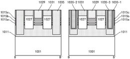
例如,如图8所示,在衬底1001的表面上,可以通过例如外延生长,形成牺牲层1013a、1013b、1013c和沟道层1015a、1015b、1015c的交替叠层。沟道层1015a、1015b、1015c随后可以形成沟道部的纳米片,厚度为例如约3nm-15nm。在生长沟道层1015a、1015b、1015c时,可以进行原位掺杂,以调节器件阈值。牺牲层1013a、1013b、1013c可以限定最下的纳米片与衬底1001之间以及相邻纳米片之间的间隙,厚度为例如约5nm-20nm。该交替叠层中牺牲层和沟道层的数目可以根据器件设计而改变,例如可以更多或更少。For example, alternate stacks of
衬底1001以及之上形成的上述各层中相邻的层相对于彼此可以具有刻蚀选择性。例如,牺牲层1013a、1013b、1013c可以包括SiGe(例如,Ge原子百分比为约20%-50%),沟道层1015a、1015b、1015c可以包括Si。The
沟道层1015a、1015b、1015c可以具有沿着衬底1001的表面延伸的形状,并因此具有相对于衬底1001的水平表面倾斜或者说不平行的表面。例如,沟道层1015a、1015b、1015c和牺牲层1013a、1013b、1013c均可以基本共形地形成在衬底1001的表面上,并可以具有大致均匀的厚度。这种情况下,沟道层1015a、1015b、1015c的倾斜表面可以与衬底1001的倾斜构造一致,并因此是例如{110}晶面族中之一。The
可以将上述叠层分离为若干部分,以分别形成针对不同器件的沟道部。例如,如图9所示,可以在叠层上形成光刻胶1017,并将其构图为覆盖要形成沟道部的区域。在形成光刻胶1017之前,可以在叠层的顶面上形成一薄的氧化物层(未示出),以保护叠层的表面,例如防止在去除光刻胶1017时的氧化和清洗等工艺损伤表面。在该示例中,形成了被光刻胶1017覆盖的三个区域(随后分别形成三个器件的沟道部)。但是,本公开不限于此。例如,可以形成更多或更少的沟道部。接着,可以光刻胶1017为掩模,对叠层进行选择性刻蚀如RIE,以使不同器件的沟道部彼此分离。在此,RIE可以进行到衬底1001中,特别是进行到阱或PTS1011之下,从而在衬底1001中形成沟槽,以便随后可以形成器件之间的隔离。沟槽可以是沿第一方向(图中进入纸面的方向)延伸的条状,从而将叠层分为沿第一方向延伸的条状。之后,可以去除光刻胶1017。The above-described stack can be separated into sections to form channel portions for different devices respectively. For example, as shown in FIG. 9, a
如图10所示,在衬底1001的沟槽中,可以形成隔离部1012。例如,可以在衬底1001上淀积氧化物,淀积的氧化物可以填充形成的沟槽,并超出叠层的顶面。可以对淀积的氧化物进行平坦化处理如化学机械抛光(CMP)。然后,可以对氧化物进行回蚀如RIE。在回蚀时,留下一定厚度的氧化物,形成隔离部1012。隔离部1012的顶面可以高于阱或PTS1011的底面,以便实现有效隔离;并可以低于叠层的最下表面,以便随后对叠层进行处理(例如,去除牺牲层)。As shown in FIG. 10, in the trenches of the
如图10中所示,限定了三个器件区域。在最左侧的器件区域中,沟道部可以具有平行于衬底1001的水平表面的表面S1以及不平行于衬底1001的水平表面的表面S2,从而呈折线形状。在最右侧的器件区域中,沟道部同样可以具有平行于衬底1001的水平表面的表面以及不平行于衬底1001的水平表面的表面,从而呈折线形状。注意,根据光刻胶1017的图案,在该器件区域中,可能有部分沟道层为不平行于衬底1001的水平表面的倾斜直线形状而非折线形状。另外,折线形状的拐点不限于图中示出的多个,而可以为单个。在中间的器件区域中,沟道部具有平行于衬底1001的水平表面的表面。As shown in Figure 10, three device regions are defined. In the leftmost device region, the channel portion may have a surface S1 parallel to the horizontal surface of the
如上所述,在衬底1001为(100)晶片的情况下,平行于衬底水平表面的表面可以为{100}晶面族中之一,而不平行于衬底水平表面的表面可以为{110}晶面族中之一。或者,在衬底1001为(110)晶片的情况下,平行于衬底水平表面的表面可以为{110}晶面族中之一,而不平行于衬底水平表面的表面可以为{100}晶面族中之一。As mentioned above, in the case where the
{100}晶面族有利于电子的迁移率。因此,表面主要为{100}晶面族的沟道部(例如,在(100)晶片的情况下,图10中的中间区域)可以用于制作n型器件。另外,{110}晶面族有利于空穴的迁移率。因此,表面主要为{110}晶面族的沟道部(例如,在(100)晶片的情况下,图10中的最右侧区域)可以用于制作p型器件。图10中的最左侧区域既有{100}晶面族的表面又有{110}晶面族的表面,因此可以用于制作p型器件或n型器件。The {100} facet family favors the mobility of electrons. Therefore, a channel portion whose surface is mainly of the {100} crystal plane family (eg, in the case of a (100) wafer, the middle region in FIG. 10 ) can be used to fabricate n-type devices. In addition, the {110} facet family is beneficial to the mobility of holes. Therefore, a channel portion whose surface is mainly of the {110} crystal plane family (eg, the rightmost region in FIG. 10 in the case of a (100) wafer) can be used to fabricate a p-type device. The leftmost region in FIG. 10 has both {100} and {110} surfaces, so it can be used to fabricate p-type devices or n-type devices.
如图11所示,可以在隔离层1012上形成牺牲栅层1019。牺牲栅层1019可以包括与牺牲层1013a、1013b、1013c类似或相同的材料,以便在随后可以通过相同的刻蚀配方来刻蚀。例如,牺牲栅层1019可以包括SiGe,其中Ge的原子百分比与牺牲层1013a、1013b、1013c中基本相同或接近,为约20%-50%。牺牲栅层1019可以通过淀积然后平坦化如CMP形成。在牺牲栅层1019上,可以通过例如淀积形成硬掩模层1021,以便于随后对牺牲栅层1019进行构图。例如,硬掩模层1021可以包括氮化物。As shown in FIG. 11 , a
可以将牺牲栅层1019构图为沿与第一方向交叉(例如,垂直)的第二方向(图中纸面内的水平方向)延伸的条形,从而形成牺牲栅。例如,如图12(a)和12(b)所示,可以在硬掩模层1021上形成光刻胶1023,并将其构图为沿第二方向延伸的条状(参见图12(b)的俯视图)。然后,如图13(a)和13(b)所示,可以光刻胶1023作为掩模,通过例如RIE依次对硬掩模层1029和牺牲栅层1019进行选择性刻蚀。于是,牺牲栅层1019被构图为沿第二方向延伸的条状。另外,还可以对所述叠层中由于牺牲栅层1019的去除而露出的沟道层和牺牲层依次进行选择性刻蚀如RIE,从而所述叠层留于牺牲栅层1019下方。刻蚀可以停止于氧化物的隔离部1012。之后,可以去除光刻胶1023。The
如图13(a)所示,当前牺牲栅层1019以及牺牲层1013a、1013b、1013c围绕沟道层1015a、1015b、1015c,它们限定了随后用于栅堆叠的空间。As shown in FIG. 13(a), the current
可以在牺牲栅层1019以及牺牲层1013a、1013b、1013c的侧壁上形成栅侧墙。例如,如图14所示,可以通过选择性刻蚀,使牺牲栅层1019以及牺牲层1013a、1013b、1013c(相对于沟道层1015a、1015b、1015c)凹入一定深度,例如凹入约2nm-7nm。为了控制凹入深度,可以采用原子层刻蚀(ALE)。在如此形成的凹入内,可以填充电介质材料,以形成栅侧墙1025。这种填充例如可以通过淀积约3nm-10nm厚的氮化物,然后对淀积的氮化物进行RIE(直至暴露沟道层的表面)来形成。在此,同为氮化物的硬掩模层1021与牺牲栅层1019侧壁上的栅侧墙可以成为一体,并因此标注为1021′。Gate spacers may be formed on the sidewalls of the
根据这种工艺,栅侧墙1025可以自对准地形成在牺牲栅层1019以及牺牲层1013a、1013b、1013c的侧壁上,而不会形成在沟道层1015a、1015b、1015c的侧壁上。栅侧墙1025可以具有实质上均匀的厚度,该厚度例如取决于上述凹入的深度。另外,栅侧墙1025的外侧壁与沟道层1015a、1015b、1015c的外侧壁可以基本上竖直对准,栅侧墙1025的内侧壁可以在竖直方向上基本对准(通过在形成凹入时控制各处的刻蚀深度基本相同来实现)。According to this process, the
之后,可以在牺牲栅层1019两侧形成与沟道层1015a、1015b、1015c的侧壁相接的源/漏部。After that, source/drain portions contacting the sidewalls of the
如图15所示,可以通过例如外延生长,形成源/漏部1027。源/漏部1027可以从暴露的衬底1001的表面以及各沟道层1015a、1015b、1015c的表面生长。生长的源/漏部源/漏部1027与各沟道层1015a、1015b、1015c的侧壁均相接。1027在生长时可以被原位掺杂为与所要形成的器件相应的导电类型,例如对于n型器件为n型,对于p型器件为p型,掺杂浓度可以为约1E19-1E21cm-3。生长的源/漏部1027可以具有与沟道层不同的材料(例如,具有不同的晶格常数),以便向沟道层施加应力。例如,对于n型器件,源/漏部1027可以包括Si:C(C原子百分比例如为约0.1%-5%);对于p型器件,源/漏部1027可以包括SiGe(Ge原子百分比例如为约20%-75%)。在衬底上同时形成n型器件和p型器件的情况下,例如在CMOS工艺的情况下,可以针对n型器件和p型器件分别生长源/漏部。在生长一种类型器件的源/漏部时,可以通过遮蔽层例如光刻胶等来遮蔽另一种类型的器件区域。As shown in FIG. 15, the source/
接下来,可以进行替代栅工艺,以完成器件制造。Next, a replacement gate process can be performed to complete device fabrication.
例如,如图16(a)和16(b)所示,可以在衬底1001上,例如通过淀积电介质材料1031如氧化物,以覆盖牺牲栅层1019、源/漏部1027和隔离部1012。可以对电介质材料1031进行平坦化处理如CMP,以露出牺牲栅层1019。For example, as shown in Figures 16(a) and 16(b), a
可以通过选择性刻蚀,去除牺牲栅层1019和牺牲层1013a、1013b、1013c(如上所述,它们可以通过相同的刻蚀配方来刻蚀),从而在栅侧墙1025内侧形成空间,可以在该空间中形成栅堆叠1029。例如,可以依次形成栅介质层1029a和栅导体层1029b(参见图17(a)和17(b))。栅介质层1029a可以大致共形的方式形成,厚度例如为约2nm-5nm,且可以包括高k栅介质如HfO2。在形成高k栅介质之前,还可以在沟道层的表面上形成界面层,例如通过氧化工艺或淀积如原子层淀积(ALD)形成的氧化物,厚度为约0.2-2nm。栅导体层1029b可以包括功函数调节金属如TiN、TaN等和栅导电金属如W等。在衬底上同时形成n型器件和p型器件的情况下,例如在CMOS工艺的情况下,可以针对n型器件和p型器件分别形成不同的栅堆叠。例如,在形成针对一种类型器件的第一栅堆叠之后,可以通过遮蔽层如光刻胶遮蔽该类型器件区域,去除另一类型器件区域中存在的第一栅堆叠(可以只去除栅导体层),且然后形成针对该另一类型器件的第二栅堆叠。The
图17(a)和17(b)以放大形式更清楚地示出了沟道层周围的栅堆叠部分。可以看出,栅堆叠位于栅侧墙1025内侧,围绕各沟道层1015a、1015b、1015c。沟道层1015a、1015b、1015c在两侧分别连接源/漏部1027,在源/漏部1027之间形成沟道。Figures 17(a) and 17(b) more clearly show the portion of the gate stack around the channel layer in enlarged form. It can be seen that the gate stack is located inside the
根据本公开的实施例,由于具有倾斜部分的沟道层的存在,从而沟道层1015a、1015b、1015c在机械上更稳定,例如在去除牺牲层1013a、1013b、1013c期间不容易弯曲或粘连,这有利于提高良品率。According to embodiments of the present disclosure, the
目前,同一源/漏部1027在相对两侧均连接到沟道层1015a、1015b、1015c。也即,这两侧的器件当前电连接在一起。可以根据设计布局,在器件之间进行电隔离。Currently, the same source/
这种电隔离可以在替代栅工艺之前进行。例如,如图18所示,在如上所述形成电介质材料1031并对其平坦化以露出牺牲栅层1019之后,可以在电介质材料1031上形成光刻胶1033,并将其构图为遮蔽一个或多个牺牲栅层1019,并露出其他牺牲栅层1019。在图18的示例中,遮蔽了中间的牺牲栅层1019,而露出了两侧的牺牲栅层1019。可以通过例如RIE,依次对露出的牺牲栅层1019以及其下方的沟道层和牺牲层进行选择性刻蚀,从而在栅侧墙1025之间留下了空间。刻蚀可以进行到阱或PTS 1011中,以实现良好的电隔离。之后,可以去除光刻胶1033。在留下的空间中,可以填充电介质材料1035如氧化物。电介质材料1035的填充可以包括淀积且然后平坦化。之后,可以进行以上描述的替代栅工艺,以形成栅堆叠1029,从而得到如图19(a)的左侧部分和19(b)所示的结构。This electrical isolation can be performed prior to the replacement gate process. For example, as shown in FIG. 18, after
根据本公开的其他实施例,可以在上述空间中例如通过依次淀积,形成多层电介质层。例如,如图19(a)的右侧部分所示,可以形成多层电介质1035-1、1035-2、1035-3的层叠结构。根据实施例,电介质层1035-1可以包括氧化物,电介质层1035-2可以包括氮化物,电介质层1035-3可以包括氮氧化物。但是,本公开不限于此。例如,可以形成更多或更少的电介质层,且电介质层可以包括其他材料。According to other embodiments of the present disclosure, multiple dielectric layers may be formed in the aforementioned spaces, eg, by sequential deposition. For example, as shown in the right part of FIG. 19( a ), a stacked structure of multilayer dielectrics 1035-1, 1035-2, and 1035-3 may be formed. According to an embodiment, the dielectric layer 1035-1 may include oxide, the dielectric layer 1035-2 may include nitride, and the dielectric layer 1035-3 may include oxynitride. However, the present disclosure is not limited thereto. For example, more or fewer dielectric layers may be formed, and the dielectric layers may include other materials.
或者,这种电隔离也可以在替代栅工艺之后进行。例如,在如以上所述进行替代栅工艺之后,可以类似地形成光刻胶以遮蔽一个或多个栅堆叠1029,而露出其他栅堆叠1029。可以通过选择性刻蚀去除露出的栅堆叠以及之下的材料层,以留下如上所述的空间,在该空间中可以填充电介质材料。Alternatively, this electrical isolation can also be performed after the replacement gate process. For example, photoresist may be similarly formed to mask one or
另外,如图19(b)所示,当前栅堆叠1029在各器件区域之间连续延伸,从而这些器件各自的栅彼此电连接。可以根据设计布局,在器件之间进行电隔离。In addition, as shown in FIG. 19( b ), the
例如,如图20(a)和20(b)所示,可以在电介质材料1031上形成光刻胶(未示出)以在需要隔离的器件区域之间露出栅堆叠1029,而遮蔽其余栅堆叠1029。之后,可以对露出的栅堆叠1029(特别是其中的栅导体层1029b)进行选择性刻蚀如RIE,刻蚀可以停止于下方的隔离部1012(或者停止于栅介质层1029a)。在由于栅堆叠1029的露出部分的刻蚀而留下的空间中,可以填充电介质材料1037如氧化物。电介质材料1037的填充可以包括淀积且然后平坦化。For example, as shown in Figures 20(a) and 20(b), a photoresist (not shown) may be formed on the
在此需要指出的是,图20(a)和20(b)示出了未进行参照图18至19(b)描述的隔离处理的情况。也可以针对图19(a)和19(b)所示的情形同样进行参照图20(a)和20(b)描述的隔离处理。这些隔离处理是否执行,根据设计布局中相邻器件之间是否需要电连接或者电隔离确定。It should be noted here that FIGS. 20( a ) and 20 ( b ) show the case where the isolation process described with reference to FIGS. 18 to 19 ( b ) is not performed. The isolation processing described with reference to FIGS. 20( a ) and 20 ( b ) can also be performed similarly to the cases shown in FIGS. 19( a ) and 19 ( b ). Whether these isolation processes are performed depends on whether electrical connection or electrical isolation is required between adjacent devices in the design layout.
图21示出了根据本公开实施例的CMOS配置的示意图。21 shows a schematic diagram of a CMOS configuration according to an embodiment of the present disclosure.
如上所述,在CMOS的情况下,可以针对n型器件和p型器件分别形成不同的栅堆叠。例如,如图21所示,在两侧的器件区域中形成p型器件且在中间的器件区域中形成n型器件的情况下,可以分别针对p型器件和n型器件形成p型栅堆叠1029p和n型栅堆叠1029n,例如它们各自具有不同的功函数。As described above, in the case of CMOS, different gate stacks may be formed for n-type devices and p-type devices, respectively. For example, as shown in FIG. 21, where p-type devices are formed in the device regions on both sides and n-type devices are formed in the middle device region, p-
在以上实施例中,通过阱或PTS 1011来抑制泄漏。本公开的实施例不限于此。例如,可以在沟道部下方形成隔离部,以抑制源漏之间的泄漏。In the above embodiments, leakage is suppressed by the trap or
图22至30示出了根据本公开另一实施例的制造半导体器件的流程中部分阶段的示意图。以下,将主要描述与上述实施例的不同之处。22 to 30 illustrate schematic diagrams of some stages in a process for fabricating a semiconductor device according to another embodiment of the present disclosure. Hereinafter, differences from the above-described embodiments will be mainly described.
可以如以上参照图1所述提供衬底1001。在衬底1001上,可以通过例如外延生长,依次形成位置限定层1002和位置保持层1004。位置限定层1002可以在随后的刻蚀中限定隔离部的底部位置,厚度为例如约5nm-20nm;位置保持层1004可以限定隔离部所占据的空间,厚度为例如约20nm-150nm。衬底1001、位置限定层1002和位置保持层1004中相邻的层相对于彼此可以具有刻蚀选择性。例如,衬底1001可以是硅晶片,位置限定层1002可以包括SiGe(例如,Ge原子百分比为约20%-50%),位置保持层1004可以包括Si。在该示例中,衬底1001和位置保持层1004均包括Si,从而在以下对位置保持层1004进行选择性刻蚀时,位置限定层1002可以限定刻蚀停止位置。但是,本公开不限于此。例如,在衬底1001和位置保持层1004包括相对于彼此具有刻蚀选择性的材料时,也可以省略位置限定层1002。The
可以进行以上参照图1至8描述的处理,从而在位置保持层1004的表面上形成倾斜构造,并形成牺牲层1013a、1013b、1013c和沟道层1015a、1015b、1015c的交替叠层。The processes described above with reference to FIGS. 1 to 8 may be performed to form a sloped structure on the surface of the
可以通过将位置保持层1004替换为电介质材料,来形成隔离部。在进行替换时,存在所述叠层相对于衬底悬空的过程。为保持所述叠层,可以形成连接到衬底的支撑部。对于同一器件区域,在一侧形成支撑部即可,而另一侧可以外露,以便进行这种替换处理。相邻的器件区域可以共用位于它们之间的支撑部。在此,以形成与上述实施例中类似的三个器件为例进行描述。这种情况下,可以形成两个支撑部。The spacers can be formed by replacing the
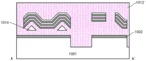
例如,如图23所示,可以在叠层上形成光刻胶1006,并将其构图为露出要形成支撑部的区域(相邻器件区域之间的区域)。在形成光刻胶1006之前,可以在叠层的顶面上形成一薄的氧化物层(未示出),以保护叠层的表面。可以光刻胶1006为掩模,对叠层进行选择性刻蚀如RIE,RIE可以进行到衬底1001中从而形成支撑部沟槽,以便随后形成的支撑部可以连接到衬底1001。之后,可以去除光刻胶1006。For example, as shown in FIG. 23, a
如图24所示,可以通过例如淀积,在衬底1001上形成电介质材料1008如氧化物。电介质材料1008可填充支撑部沟槽,并可以覆盖叠层。可以对淀积的电介质材料1008进行平坦化处理如CMP。填充在支撑部沟槽中的电介质材料1008可以形成支撑部。As shown in FIG. 24, a
另外,可以将叠层在不同器件区域之间分离。在该示例中,由于支撑部的形成,各器件区域已在一侧与相邻器件区域相分离,只需在另一侧进行分离即可。例如,如图25所示,可以在电介质材料1008上形成光刻胶1010,并将其构图为露出相邻器件区域之间的区域(形成支撑部之处无需再露出)。可以光刻胶1010为掩模,对叠层进行选择性刻蚀如RIE,从而形成隔离沟槽,以使不同器件的沟道部彼此分离。在此,RIE可以进行到位置保持层1004中,但是并未到达位置限定层1002(在以下形成保护层的情况下,这可以避免保护层将位置保持层1004完全遮挡从而无法被替换)。之后,可以去除光刻胶1010。Additionally, the stack can be separated between different device regions. In this example, due to the formation of the support portion, each device region has been separated from the adjacent device region on one side, and only needs to be separated on the other side. For example, as shown in FIG. 25, a
接着,可以将位置保持层1004替换为绝缘体。为了在去除位置保持层1004的过程中保护叠层特别是其中的沟道层(特别是在该示例中,沟道层与位置保持层1004均包括Si),可以在叠层的侧壁上形成保护层。例如,如图26所示,可以通过侧墙形成工艺,在叠层的暴露侧壁上形成保护层。在该示例中,保护层可以包括氧化物,并因此与同为氧化物的电介质材料1008一体示出为1008′。Next, the
如图27所示,可以通过选择性刻蚀,去除位置保持层1004。一方面,支撑部可以将叠层相对于衬底1001悬空支撑;另一方面,隔离沟槽可以形成对叠层下方的位置保持层1004进行刻蚀的加工通道。例如,可以使用TMAH溶液,相对于支撑部(在该示例中为氧化物)以及位置限定层1002和牺牲层1013a(在该示例中为SiGe)来选择性刻蚀位置保持层1004(在该示例中为Si)。As shown in FIG. 27, the
如图28所示,可以通过隔离沟槽,向叠层下方填充电介质材料以形成隔离部。这种填充可以通过淀积如化学气相淀积(CVD)、原子层淀积(ALD)等进行。取决于叠层下方空间的大小以及淀积工艺的填充性能,在叠层下方可能并未完全填满电介质材料,而可能存在气隙1014。为改进填充性能,可以采用重复淀积并刻蚀的方法。另外,隔离沟槽中也可以填充了电介质材料,形成器件之间的隔离部。填充的电介质材料可以包括氧化物,且因此与之前的电介质材料1008′一起示出为1012′。As shown in FIG. 28, isolation trenches may be used to fill the lower layers of the stack with dielectric material to form isolations. This filling can be performed by deposition such as chemical vapor deposition (CVD), atomic layer deposition (ALD), and the like. Depending on the size of the space under the stack and the filling properties of the deposition process, the dielectric material may not be completely filled under the stack, and
如图29所示,可以对电介质材料1012′进行回蚀,从而形成隔离部。回蚀后电介质材料1012′的顶面可以高于位置限定层1002,以便实现有效隔离;并可以低于叠层的最下表面,以便随后对叠层进行处理(例如,去除牺牲层)。可以看到,隔离部1012′一方面设置在相邻器件之间,形成相邻器件之间的电隔离例如STI(浅沟槽隔离);另一方面设置的沟道部下方,抑制相同器件中源漏之间的泄漏。As shown in FIG. 29, the dielectric material 1012' may be etched back to form the spacers. The top surface of the post-etch back dielectric material 1012' may be higher than the
之后,可以按以上参照图11至20(b)描述的工艺,得到如图30所示的半导体器件。After that, the semiconductor device shown in FIG. 30 can be obtained by the processes described above with reference to FIGS. 11 to 20(b).
根据本公开实施例的半导体器件可以应用于各种电子设备。例如,可以基于这样的半导体器件形成集成电路(IC),并由此构建电子设备。因此,本公开还提供了一种包括上述半导体器件的电子设备。电子设备还可以包括与集成电路配合的显示屏幕以及与集成电路配合的无线收发器等部件。这种电子设备例如智能电话、计算机、平板电脑(PC)、人工智能设备、可穿戴设备、移动电源等。The semiconductor device according to the embodiment of the present disclosure can be applied to various electronic devices. For example, integrated circuits (ICs) can be formed based on such semiconductor devices, and electronic devices can be constructed therefrom. Accordingly, the present disclosure also provides an electronic device including the above-described semiconductor device. The electronic device may also include components such as a display screen cooperating with the integrated circuit and a wireless transceiver cooperating with the integrated circuit. Such electronic devices are, for example, smartphones, computers, tablet computers (PCs), artificial intelligence devices, wearable devices, power banks, and the like.
根据本公开的实施例,还提供了一种芯片系统(SoC)的制造方法。该方法可以包括上述方法。具体地,可以在芯片上集成多种器件,其中至少一些是根据本公开的方法制造的。According to an embodiment of the present disclosure, a method of fabricating a system on a chip (SoC) is also provided. The method may include the methods described above. Specifically, a variety of devices can be integrated on a chip, at least some of which are fabricated according to the methods of the present disclosure.
在以上的描述中,对于各层的构图、刻蚀等技术细节并没有做出详细的说明。但是本领域技术人员应当理解,可以通过各种技术手段,来形成所需形状的层、区域等。另外,为了形成同一结构,本领域技术人员还可以设计出与以上描述的方法并不完全相同的方法。另外,尽管在以上分别描述了各实施例,但是这并不意味着各个实施例中的措施不能有利地结合使用。In the above description, technical details such as patterning and etching of each layer are not described in detail. However, those skilled in the art should understand that various technical means can be used to form layers, regions, etc. of desired shapes. In addition, in order to form the same structure, those skilled in the art can also design methods that are not exactly the same as those described above. Additionally, although the various embodiments have been described above separately, this does not mean that the measures in the various embodiments cannot be used in combination to advantage.
以上对本公开的实施例进行了描述。但是,这些实施例仅仅是为了说明的目的,而并非为了限制本公开的范围。本公开的范围由所附权利要求及其等价物限定。不脱离本公开的范围,本领域技术人员可以做出多种替代和修改,这些替代和修改都应落在本公开的范围之内。Embodiments of the present disclosure have been described above. However, these examples are for illustrative purposes only, and are not intended to limit the scope of the present disclosure. The scope of the present disclosure is defined by the appended claims and their equivalents. Without departing from the scope of the present disclosure, those skilled in the art can make various substitutions and modifications, and these substitutions and modifications should all fall within the scope of the present disclosure.
Claims (41)
Priority Applications (3)
| Application Number | Priority Date | Filing Date | Title |
|---|---|---|---|
| CN202010282958.XA CN111446292B (en) | 2020-04-10 | 2020-04-10 | Semiconductor device and method for manufacturing the same, and electronic device including the same |
| PCT/CN2021/079982 WO2021203901A1 (en) | 2020-04-10 | 2021-03-10 | Semiconductor device and fabrication method therefor, and electronic device comprising same |
| US17/995,698 US20230135187A1 (en) | 2020-04-10 | 2021-03-10 | Semiconductor device, method of manufacturing the same, and electronic apparatus including the same |
Applications Claiming Priority (1)
| Application Number | Priority Date | Filing Date | Title |
|---|---|---|---|
| CN202010282958.XA CN111446292B (en) | 2020-04-10 | 2020-04-10 | Semiconductor device and method for manufacturing the same, and electronic device including the same |
Publications (2)
| Publication Number | Publication Date |
|---|---|
| CN111446292A true CN111446292A (en) | 2020-07-24 |
| CN111446292B CN111446292B (en) | 2024-04-26 |
Family
ID=71651519
Family Applications (1)
| Application Number | Title | Priority Date | Filing Date |
|---|---|---|---|
| CN202010282958.XA Active CN111446292B (en) | 2020-04-10 | 2020-04-10 | Semiconductor device and method for manufacturing the same, and electronic device including the same |
Country Status (3)
| Country | Link |
|---|---|
| US (1) | US20230135187A1 (en) |
| CN (1) | CN111446292B (en) |
| WO (1) | WO2021203901A1 (en) |
Cited By (2)
| Publication number | Priority date | Publication date | Assignee | Title |
|---|---|---|---|---|
| WO2021203901A1 (en) * | 2020-04-10 | 2021-10-14 | 中国科学院微电子研究所 | Semiconductor device and fabrication method therefor, and electronic device comprising same |
| WO2021203899A1 (en) * | 2020-04-10 | 2021-10-14 | 中国科学院微电子研究所 | Semiconductor device, fabrication method for same, and electronic device comprising same |
Families Citing this family (1)
| Publication number | Priority date | Publication date | Assignee | Title |
|---|---|---|---|---|
| CN114623777B (en) * | 2022-02-21 | 2022-11-18 | 武汉大学 | Construction method and measurement method of measurement model of stacked nanosheet structure |
Citations (4)
| Publication number | Priority date | Publication date | Assignee | Title |
|---|---|---|---|---|
| CN101427374A (en) * | 2006-04-28 | 2009-05-06 | 国际商业机器公司 | High performance 3D FET structures, and methods for forming the same using preferential crystallographic etching |
| US20180114727A1 (en) * | 2016-10-24 | 2018-04-26 | Samsung Electronics Co., Ltd. | Field effect transistor with stacked nanowire-like channels and methods of manufacturing the same |
| US20190348541A1 (en) * | 2018-05-14 | 2019-11-14 | Synopsys, Inc. | Crystal orientation engineering to achieve consistent nanowire shapes |
| CN110828378A (en) * | 2018-08-14 | 2020-02-21 | 台湾积体电路制造股份有限公司 | Method of forming semiconductor device |
Family Cites Families (7)
| Publication number | Priority date | Publication date | Assignee | Title |
|---|---|---|---|---|
| CN101719501B (en) * | 2009-12-01 | 2011-07-20 | 中国科学院上海微系统与信息技术研究所 | Hybrid orientation inversion mode all-around-gate CMOS field effect transistor |
| US9741811B2 (en) * | 2014-12-15 | 2017-08-22 | Samsung Electronics Co., Ltd. | Integrated circuit devices including source/drain extension regions and methods of forming the same |
| US9984936B1 (en) * | 2017-07-17 | 2018-05-29 | Globalfoundries Inc. | Methods of forming an isolated nano-sheet transistor device and the resulting device |
| US10971585B2 (en) * | 2018-05-03 | 2021-04-06 | International Business Machines Corporation | Gate spacer and inner spacer formation for nanosheet transistors having relatively small space between adjacent gates |
| US11335807B2 (en) * | 2018-06-29 | 2022-05-17 | Intel Corporation | Isolation schemes for gate-all-around transistor devices |
| CN111463287B (en) * | 2020-04-10 | 2024-02-27 | 中国科学院微电子研究所 | Semiconductor device and manufacturing method thereof and electronic equipment including the same |
| CN111446292B (en) * | 2020-04-10 | 2024-04-26 | 中国科学院微电子研究所 | Semiconductor device and method for manufacturing the same, and electronic device including the same |
-
2020
- 2020-04-10 CN CN202010282958.XA patent/CN111446292B/en active Active
-
2021
- 2021-03-10 WO PCT/CN2021/079982 patent/WO2021203901A1/en not_active Ceased
- 2021-03-10 US US17/995,698 patent/US20230135187A1/en active Pending
Patent Citations (4)
| Publication number | Priority date | Publication date | Assignee | Title |
|---|---|---|---|---|
| CN101427374A (en) * | 2006-04-28 | 2009-05-06 | 国际商业机器公司 | High performance 3D FET structures, and methods for forming the same using preferential crystallographic etching |
| US20180114727A1 (en) * | 2016-10-24 | 2018-04-26 | Samsung Electronics Co., Ltd. | Field effect transistor with stacked nanowire-like channels and methods of manufacturing the same |
| US20190348541A1 (en) * | 2018-05-14 | 2019-11-14 | Synopsys, Inc. | Crystal orientation engineering to achieve consistent nanowire shapes |
| CN110828378A (en) * | 2018-08-14 | 2020-02-21 | 台湾积体电路制造股份有限公司 | Method of forming semiconductor device |
Cited By (3)
| Publication number | Priority date | Publication date | Assignee | Title |
|---|---|---|---|---|
| WO2021203901A1 (en) * | 2020-04-10 | 2021-10-14 | 中国科学院微电子研究所 | Semiconductor device and fabrication method therefor, and electronic device comprising same |
| WO2021203899A1 (en) * | 2020-04-10 | 2021-10-14 | 中国科学院微电子研究所 | Semiconductor device, fabrication method for same, and electronic device comprising same |
| US12543356B2 (en) | 2020-04-10 | 2026-02-03 | Institute of Microelectronics, Chinese Academy of Sciences | Semiconductor device, fabrication method for same, and electronic device comprising same |
Also Published As
| Publication number | Publication date |
|---|---|
| US20230135187A1 (en) | 2023-05-04 |
| WO2021203901A1 (en) | 2021-10-14 |
| CN111446292B (en) | 2024-04-26 |
Similar Documents
| Publication | Publication Date | Title |
|---|---|---|
| US20260013208A1 (en) | Selective removal of semiconductor fins | |
| CN111584486B (en) | Semiconductor device having staggered structure, method of manufacturing the same, and electronic apparatus | |
| TWI762921B (en) | Semiconductor device, method for manufacturing the same, and electronic equipment including the same | |
| CN111106111B (en) | Semiconductor device, method of manufacturing the same, and electronic apparatus including the same | |
| CN111463287B (en) | Semiconductor device and manufacturing method thereof and electronic equipment including the same | |
| CN111106176B (en) | Semiconductor device, method of manufacturing the same, and electronic apparatus including the same | |
| KR102807518B1 (en) | Nanowire/sheet devices having self-aligning isolation regions, methods for fabricating them, and electronic devices | |
| CN111446292B (en) | Semiconductor device and method for manufacturing the same, and electronic device including the same | |
| US12588233B2 (en) | Semiconductor device having U-shaped structure, method of manufacturing semiconductor device, and electronic device | |
| CN105390497A (en) | CMOS device including charged body spacers and method of manufacturing the same | |
| CN112018184A (en) | Device with ferroelectric or negative capacitance material, method of manufacturing the same, and electronic apparatus | |
| CN104681563B (en) | Semiconductor device and manufacturing method thereof | |
| US20240379794A1 (en) | 3ds fet and method of manufacturing the same |
Legal Events
| Date | Code | Title | Description |
|---|---|---|---|
| PB01 | Publication | ||
| PB01 | Publication | ||
| SE01 | Entry into force of request for substantive examination | ||
| SE01 | Entry into force of request for substantive examination | ||
| GR01 | Patent grant | ||
| GR01 | Patent grant |