CN111213389B - Current measurement at the output of a switching amplifier - Google Patents
Current measurement at the output of a switching amplifier Download PDFInfo
- Publication number
- CN111213389B CN111213389B CN201880068257.7A CN201880068257A CN111213389B CN 111213389 B CN111213389 B CN 111213389B CN 201880068257 A CN201880068257 A CN 201880068257A CN 111213389 B CN111213389 B CN 111213389B
- Authority
- CN
- China
- Prior art keywords
- current
- switch
- load
- transistor switch
- coupled
- Prior art date
- Legal status (The legal status is an assumption and is not a legal conclusion. Google has not performed a legal analysis and makes no representation as to the accuracy of the status listed.)
- Active
Links
- 238000005259 measurement Methods 0.000 title description 28
- 230000004044 response Effects 0.000 claims abstract description 22
- 238000000034 method Methods 0.000 claims abstract description 21
- 230000007704 transition Effects 0.000 claims description 30
- 229910044991 metal oxide Inorganic materials 0.000 claims description 6
- 150000004706 metal oxides Chemical class 0.000 claims description 6
- 239000004065 semiconductor Substances 0.000 claims description 6
- 230000005669 field effect Effects 0.000 claims description 4
- 230000005236 sound signal Effects 0.000 description 9
- 230000000295 complement effect Effects 0.000 description 7
- 230000008569 process Effects 0.000 description 7
- 238000010586 diagram Methods 0.000 description 5
- 230000008901 benefit Effects 0.000 description 3
- 238000005070 sampling Methods 0.000 description 3
- 239000003990 capacitor Substances 0.000 description 2
- 239000002131 composite material Substances 0.000 description 2
- 230000003321 amplification Effects 0.000 description 1
- 238000006243 chemical reaction Methods 0.000 description 1
- 230000000694 effects Effects 0.000 description 1
- 239000000463 material Substances 0.000 description 1
- 238000012986 modification Methods 0.000 description 1
- 230000004048 modification Effects 0.000 description 1
- 238000003199 nucleic acid amplification method Methods 0.000 description 1
- 230000001052 transient effect Effects 0.000 description 1
Images

Classifications
-
- G—PHYSICS
- G01—MEASURING; TESTING
- G01R—MEASURING ELECTRIC VARIABLES; MEASURING MAGNETIC VARIABLES
- G01R19/00—Arrangements for measuring currents or voltages or for indicating presence or sign thereof
- G01R19/165—Indicating that current or voltage is either above or below a predetermined value or within or outside a predetermined range of values
- G01R19/16566—Circuits and arrangements for comparing voltage or current with one or several thresholds and for indicating the result not covered by subgroups G01R19/16504, G01R19/16528, G01R19/16533
- G01R19/16571—Circuits and arrangements for comparing voltage or current with one or several thresholds and for indicating the result not covered by subgroups G01R19/16504, G01R19/16528, G01R19/16533 comparing AC or DC current with one threshold, e.g. load current, over-current, surge current or fault current
-
- H—ELECTRICITY
- H02—GENERATION; CONVERSION OR DISTRIBUTION OF ELECTRIC POWER
- H02H—EMERGENCY PROTECTIVE CIRCUIT ARRANGEMENTS
- H02H9/00—Emergency protective circuit arrangements for limiting excess current or voltage without disconnection
- H02H9/02—Emergency protective circuit arrangements for limiting excess current or voltage without disconnection responsive to excess current
- H02H9/025—Current limitation using field effect transistors
-
- H—ELECTRICITY
- H03—ELECTRONIC CIRCUITRY
- H03F—AMPLIFIERS
- H03F3/00—Amplifiers with only discharge tubes or only semiconductor devices as amplifying elements
- H03F3/181—Low-frequency amplifiers, e.g. audio preamplifiers
- H03F3/183—Low-frequency amplifiers, e.g. audio preamplifiers with semiconductor devices only
- H03F3/185—Low-frequency amplifiers, e.g. audio preamplifiers with semiconductor devices only with field-effect devices
-
- H—ELECTRICITY
- H03—ELECTRONIC CIRCUITRY
- H03F—AMPLIFIERS
- H03F3/00—Amplifiers with only discharge tubes or only semiconductor devices as amplifying elements
- H03F3/20—Power amplifiers, e.g. Class B amplifiers, Class C amplifiers
- H03F3/21—Power amplifiers, e.g. Class B amplifiers, Class C amplifiers with semiconductor devices only
- H03F3/217—Class D power amplifiers; Switching amplifiers
- H03F3/2173—Class D power amplifiers; Switching amplifiers of the bridge type
-
- H—ELECTRICITY
- H04—ELECTRIC COMMUNICATION TECHNIQUE
- H04R—LOUDSPEAKERS, MICROPHONES, GRAMOPHONE PICK-UPS OR LIKE ACOUSTIC ELECTROMECHANICAL TRANSDUCERS; DEAF-AID SETS; PUBLIC ADDRESS SYSTEMS
- H04R3/00—Circuits for transducers, loudspeakers or microphones
- H04R3/007—Protection circuits for transducers
-
- G—PHYSICS
- G11—INFORMATION STORAGE
- G11C—STATIC STORES
- G11C27/00—Electric analogue stores, e.g. for storing instantaneous values
- G11C27/02—Sample-and-hold arrangements
- G11C27/024—Sample-and-hold arrangements using a capacitive memory element
-
- H—ELECTRICITY
- H04—ELECTRIC COMMUNICATION TECHNIQUE
- H04R—LOUDSPEAKERS, MICROPHONES, GRAMOPHONE PICK-UPS OR LIKE ACOUSTIC ELECTROMECHANICAL TRANSDUCERS; DEAF-AID SETS; PUBLIC ADDRESS SYSTEMS
- H04R2499/00—Aspects covered by H04R or H04S not otherwise provided for in their subgroups
- H04R2499/10—General applications
- H04R2499/11—Transducers incorporated or for use in hand-held devices, e.g. mobile phones, PDA's, camera's
Landscapes
- Engineering & Computer Science (AREA)
- Power Engineering (AREA)
- Physics & Mathematics (AREA)
- Multimedia (AREA)
- Acoustics & Sound (AREA)
- Signal Processing (AREA)
- General Physics & Mathematics (AREA)
- Amplifiers (AREA)
- Circuit For Audible Band Transducer (AREA)
Abstract
Systems and methods for sensing current at an output of a switching amplifier include: a first transistor switch coupled to the load configured to conduct current in the load in response to a first pulse width modulation control signal coupled to a first gate terminal of the first transistor switch. The second transistor switch is configured to conduct current in the load in response to a second pulse width modulation control signal coupled to a second gate terminal of the second transistor switch. A shield switch is coupled between the load and the current sensing circuit, wherein the shield switch is configured to provide a small-signal voltage to the current sensing circuit in response to the second pulse width modulation control signal, the current sensing circuit configured to sense a current through the load in response to the small-signal voltage.
Description
Cross Reference to Related Applications
This application claims the benefit and priority of U.S. patent application No. 15/789,907 filed on 2017, 10, 20, which is hereby incorporated by reference in its entirety.
Technical Field
In accordance with one or more embodiments, the present disclosure relates generally to signal processing, and more particularly, for example, to sensing current at an output of a switching amplifier.
Background
Many modern devices, such as laptop computers, computer tablets, MP3 players, and smart phones, use micro speakers. In many applications, these devices utilize switching amplifiers to efficiently provide amplification of audio signals. In one example, the switching amplifier may provide twenty watts of power to amplify the audio signal and drive the speaker. Due to the limitations of miniature speakers used in such devices, the current to the speaker can be measured to help prevent distortion, physical damage to the speaker, and other unwanted effects. Thus, there is a continuing need for: the measurement of the current supplied to the loudspeaker by the switching amplifier is improved to protect the loudspeaker from distortion or damage.
Disclosure of Invention
The present disclosure provides systems and methods that address the need in the art for accurately sensing the current provided by a switching amplifier to a load. The scope of the present disclosure is defined by the claims, which are incorporated into this section by reference. A more complete understanding of the present disclosure will be afforded to those skilled in the art, as well as a realization of additional advantages thereof, by a consideration of the following detailed description of one or more embodiments. Reference will be made to the appended sheets of drawings, which will first be described briefly.
Drawings
Aspects of the present disclosure and its advantages are better understood by referring to the following drawings and detailed description that follows. It should be appreciated that like reference numerals are used to identify like elements illustrated in one or more of the figures, where the illustrations in the figures are for the purpose of illustrating embodiments of the disclosure and are not for the purpose of limiting the embodiments of the disclosure. The components in the figures are not necessarily to scale, emphasis instead being placed upon clearly illustrating the principles of the present disclosure.
Fig. 1 illustrates an exemplary audio codec according to one or more embodiments of the present disclosure.
Fig. 2 illustrates a schematic diagram of an exemplary audio amplifier output driver in accordance with one or more embodiments of the present disclosure.
Fig. 3 illustrates exemplary curves of sense current and control voltage of an audio amplifier output driver according to an embodiment of the disclosure.
Fig. 4 illustrates a schematic diagram of an exemplary audio amplifier output driver including a sample and hold circuit in accordance with one or more embodiments of the present disclosure.
Fig. 5 illustrates an example process flow for an audio amplifier output driver speaker protection system in accordance with one or more embodiments of the present disclosure.
Detailed Description
The present disclosure describes systems and methods that address the need for accurately measuring the current provided by a switching amplifier, such as a switching regulator or a class D switching amplifier. In one embodiment, an audio system of the present disclosure includes a switching amplifier H-bridge output stage and one or more output current measurement circuits. Each output current measurement circuit comprises a current sensing component (such as a current mirror circuit) and a shield switch arranged to provide an accurate measurement of the current through the load during all phases of the amplifier switching, including switching amplifier output state transitions.
Embodiments of the present disclosure may be contrasted with existing solutions for measuring the current at the output of a switching regulator or class D switching amplifier. For example, a conventional switching amplifier current sensing circuit may use a sense resistor mounted in series with the load to sense the current through the load. A sense amplifier connected to a sense resistor may require a relatively large common mode rejection ratio to handle large switching amplifier output voltage variations at the sense resistor. Many passive current sensing circuits reduce efficiency in the operation of the H-bridge amplifier output stage by additional power dissipation losses within the system. Furthermore, the added power dissipation may cause thermal problems for applications including switching amplifier circuits formed within an integrated circuit die.
Some conventional audio systems use a current mirror circuit for load current sensing measurements. However, the performance of the current mirror circuit may be affected by similar common mode limitations as discussed herein. For example, conventional current mirror circuits used with switching amplifier applications may be subject to large voltage swings, requiring current mirror circuits with relatively high common mode rejection ratios. Furthermore, the current mirror circuit does not provide accurate current measurement when the switching transistor is in a transition between the "on" and "off" states. Various embodiments of the present disclosure address these issues to accurately and efficiently measure the current provided to a load by a switching amplifier to protect a load, such as a speaker, from distortion or damage.
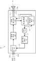
Fig. 1 illustrates a block diagram of an exemplary audio codec circuit 100 in accordance with one or more embodiments of the present disclosure. The audio codec circuit 100 provides analog and digital circuits for signal processing of audio inputs. The audio codec circuit 100 includes circuitry to process an input digital signal and provide an amplified output signal to a speaker for an output device 121. In some embodiments, the audio codec circuit 100 receives digital signals at input ports 105A-B. The digital signal may be provided, for example, by any electronic device such as a laptop computer, computer tablet, smart phone, or a sensor such as a microphone.
A digital-to-analog converter (DAC) 107 may be configured to receive the digital signal and convert the digital signal to an analog signal for further processing. The control circuit 109 receives the analog audio signal from the DAC 107 and processes the analog audio signal. In some embodiments, the control circuit 109 provides a pulse width modulated signal to the audio amplifier 108. In some embodiments, the audio amplifier 108 is implemented as a class D switching amplifier, and the pulse width modulated signal controls the switching duty cycle of the audio amplifier 108. The audio amplifier 108 amplifies the received analog audio signals and provides amplified audio signals 131A-B to drive the output devices 121 at the output jacks 119A-B. The output device 121 may be a microphone, an earphone, or another electronic device for receiving the amplified audio signals 131A-B.
The audio amplifier 108 is electrically coupled to a current measurement circuit 110. The current measurement circuit 110 is configured to sense a current signal traveling to the output device 121 at the low side output switch of the audio amplifier 108. In some embodiments, the current measurement circuit 110 provides an approximation of the current signal through the output device 121. In some embodiments, a current mirror circuit within the current measurement circuit 110 provides and measures the equivalent current. As illustrated, the measured current signal 120 is provided to the overcurrent protection circuit 117. In some embodiments, if the measured current signal 120 exceeds the upper current threshold, the over-current protection circuit 117 adjusts the frequency of the pulse width modulated signal to reduce the amplitude of the current traveling to the output device 121. The upper current threshold may be the maximum current that the output device 121 can withstand without distortion or physical damage, and may depend on the materials and processes used to fabricate the output device 121. For example, micro-speakers used in modern electronic devices may be able to withstand a steady state of approximately five hundred milliamps. In other embodiments, the over-current protection circuit 117 provides the over-current control signal 118 to turn off the audio amplifier 108 if the measured current signal 120 exceeds the upper current threshold.
The current measurement circuit 110 is operable to provide an equivalent current to the instantaneous current traveling to the output device 121 when the low side output switch is active. The current measurement circuit 110 is also operable to provide an equivalent current to the load current when the low-side output switch and the high-side output switch transition between the "on" and "off states. In this regard, current measurement circuit 110 and overcurrent protection circuit 117 function to adjust the current by comparing the measured current signal 120 to an upper current threshold and in response to the threshold being exceeded to robustly protect the output device 121 from transient distortion or physical damage.
The current measurement circuit 110 may also provide an analog voltage equivalent to the measured current signal 120 to the speaker protection circuit 111. In the illustrated embodiment, an analog-to-digital converter (ADC) 113 converts the analog voltage to a digital voltage signal 122 representative of the measured current signal 120. The ADC 113 provides the digital voltage signal 122 to the speaker protection circuit 111, and the speaker protection circuit 111 further processes the digital voltage signal 122. In some embodiments, the speaker protection circuit 111 provides a signal 114 to the DAC 107 to adjust DAC 107 signal processing based on measured current feedback to protect an output device 121 (e.g., a speaker).
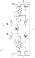
Fig. 2 illustrates a schematic diagram of an exemplary audio amplifier output driver 200, in accordance with an embodiment of the present disclosure. In some embodiments, the audio amplifier output driver 200 forms part of the audio amplifier 108 implemented in the audio codec circuit 100. The audio amplifier output driver 200 provides audio output to drive a speaker load 235, which may be implemented in a mobile phone, laptop, tablet, audio/video system, or other similar device. In various embodiments, the audio amplifier output driver 200 is implemented as a class D amplifier, H-bridge output stage 201. The audio amplifier output driver 200 is coupled to one or more current measurement circuits 210.
As shown in fig. 2, in some embodiments, the H-bridge output stage 201 includes four n-channel laterally diffused Metal Oxide Semiconductor Field Effect Transistors (MOSFETs) M1, M2, M3, and M4. The respective drains of the first two high-side transistors M3, M4 are connected to the supply voltage Pvdd. In some embodiments, the supply voltage Pvdd provides twelve volts of DC power to the transistors M3, M4. However, in other embodiments, other supply voltages may be provided. The respective sources are connected to the drains of the two low side transistors M1, M2, the sources of which are connected to the ground signal 221. The speaker load 235 is connected between the transistor switch pair M3, M1 and M4, M2. The control circuit 109 of fig. 1 may provide a pulse width modulation control signal 202 to the gates of transistors M1, M2, M3, and M4. In some embodiments, the first pulse width modulation (PMW) control signal 202 is connected to the gate terminal of the transistor M3, the second PMW control signal 202 is connected to the gate terminal of the transistor M1, the third PMW control signal 202 is connected to the gate terminal of the transistor M4, and the fourth PMW control signal 202 is connected to the gate terminal of the transistor M2.
In some embodiments, the first current measurement circuit 210 includes a current mirror amplifier 211 (e.g., a current sensing circuit), n-channel MOS transistors S1 and S2, a shield switch 224, and a pull-down resistor 225. In this arrangement, the current Ispk through the speaker load 235 is represented by the equivalent measured currents Isensep and Isensen.
The current mirror amplifier 211 includes two input terminals: a non-inverting input terminal 212 and an inverting input terminal 214. The non-inverting input terminal 212 is connected to the source terminal of the shield switch 224. The drain terminal of the shield switch 224 is connected to the source terminal of the transistor M3 (e.g., a first transistor switch) and the drain terminal of the transistor M1 (e.g., a second transistor switch). The inverting input terminal 214 of the current mirror amplifier 211 is connected to the source terminal of the transistor S1 and the drain terminal of the transistor S2. The current mirror amplifier 211 output signal 216 is connected to the gate terminal of transistor S1 to drive transistor S1. The source terminal of the transistor S2 is connected to the ground signal 221. The drain terminal of transistor S1 is connected to the Isensep current signal.
The gate terminal of the shield switch 224 is connected to the gate terminal of the low side transistor M1. When the second PWM control signal 202 turns on the transistor M1, the shield switch 224 turns on in response to the second PWM control signal 202 and provides a small-signal DC voltage at node Va that is equivalent to the voltage at the drain terminal of M1. In some embodiments, the small-signal DC voltage is approximately fifty to one hundred millivolts. Node Va is connected to the non-inverting input terminal of 212 of current mirror amplifier 211 to provide voltage Va to current mirror amplifier 211. The current mirror amplifier 211 output signal 216 controls the gate voltage of S1 to adjust the drain-source voltage across S2. In this regard, the voltage across transistor M1 and equivalently at node Va is mirrored across transistor S1 to provide an isencep current signal through switches S1 and S2 that is approximately equal to the load current Ispk. In some embodiments, the current mirror amplifier 211 is implemented as a laterally diffused metal oxide semiconductor circuit. A pull-down resistor 225 is connected between node Va (e.g., at the source terminal of the shield switch 224) and the ground signal 221 to provide a fast transition to zero volts at node Va when the shield switch 224 is turned off.
In some embodiments, the complementary second current measurement circuit 210B includes current mirror amplifier 211B, n channel MOS transistors S3 and S4, shield switch 224B, and pull-down resistor 225B. The current Ispk through the speaker load 235 at the H-bridge complementary transistor pair (e.g., M4 and M2) is represented by the equivalent measured current Isensen.
The current mirror amplifier 211B includes two input terminals, a non-inverting input terminal 215 and an inverting input terminal 217. The non-inverting input terminal 215 is connected to the source terminal of the shield switch 224B. The drain terminal of the shield switch 224B is connected to the source terminal of the transistor M4 (e.g., the third transistor switch) and the drain terminal of the transistor M2 (e.g., the fourth transistor switch). The inverting input terminal 217 of the current mirror amplifier 211B is connected to the source terminal of the transistor S3 and the drain terminal of the transistor S4. The current mirror amplifier 211B output signal 219 is connected to the gate terminal of transistor S3 to drive transistor S3. The source terminal of the transistor S4 is connected to the ground signal 221. The drain terminal of transistor S1 is connected to the Isensen current signal.
The gate terminal of the shield switch 224B is connected to the gate terminal of the low side transistor M2. When the fourth PWM control signal 202 turns on transistor M2, the shield switch 224B turns on in response to the fourth PWM control signal 202 and provides a small-signal DC voltage of approximately fifty millivolts at node Vab, which is connected to the source terminal of the shield switch 224B. Node Va is connected to the non-inverting input terminal of 215 of current mirror amplifier 211B to provide voltage Va to current mirror amplifier 211B. Current mirror amplifier 211B output signal 219 controls the gate voltage of S3 to control the drain-source voltage at S4 and provide current Isensen which mirrors load current Ispk. A pull-down resistor 225B is connected between node Vab and the ground signal 221 to provide a fast transition to zero volts at node Vab when the shield switch 224B is open. When the audio amplifier output driver 200 is powered on, the power supply Avdd is connected to the gates of the transistors S2 and S4 to turn on the transistors S2 and S4.
As shown in fig. 2, transistors S2 and S4 mirror the current flowing in the speaker load 235, as discussed herein. The speaker load 235 is connected between the source of M3 and the drain of M1 on a first end and between the source of M4 and the drain of M2 on a second end. When M1 is conducting, transistor S2 mirrors the current flowing through transistor M1 (e.g., the second transistor switch) during the PWM cycle. The transistor S4 mirrors the current flowing through the transistor M2 (e.g., the fourth transistor switch) during the PWM cycle of M2 conduction. In this regard, the speaker load 235 current is sensed for the full range of Ispk current as Ispk flows through the combined transistors M1 and M2.
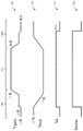
Fig. 3 illustrates plots of sense current and control voltage for an audio amplifier output driver according to an embodiment of the present disclosure. Fig. 3 shows a plot 305 of the gate voltage Vgate at the gate terminals of the transistor switch M1 and the shield switch 224 during the first transition 340 and the second transition 340B. As shown, a first transition 340 illustrates a transition of Vgate from zero volts to five volts. A second transition 340B illustrates the transition of Vgate from five volts to zero volts. During the first transition 340, the transistor switch M3 (e.g., a first transistor switch) is turned off and the transistor switch M1 (e.g., a second transistor switch) is turned on. During the second transition 340B, the transistor switch M3 (e.g., the first transistor switch) is turned on and the transistor switch M1 (e.g., the second transistor switch) is turned off. The second PWM control signal 202 controls the transistor switch M1 and the shield switch 224 to be turned on and off. The fourth PWM control signal 202 controls the transistor switch M2 and the shield switch 224B to be turned on and off.
Fig. 4 illustrates a schematic diagram of an exemplary audio amplifier output driver 200 including a sample and hold circuit 425, according to an embodiment of the disclosure. The sample and hold circuit 425 is arranged to receive a small DC signal voltage (e.g., a small signal DC voltage such as approximately fifty millivolts) from the source of the shield switch 224 and provide the small DC signal voltage to the current mirror amplifier 211 for a predetermined sampling period. As shown in fig. 4, sample and hold circuit 425 is coupled between the source terminal of shield switch 224 and non-inverting input terminal 212 of current mirror amplifier 211.
In some embodiments, sample and hold circuit 425 is implemented as a capacitor, a field effect transistor switch, and an operational amplifier. For example, the operational amplifier charges or discharges a capacitor to approximately the voltage level at the input, such as a small signal voltage. The charging voltage is switched to the output of the sample and hold circuit 425 and provided to the non-inverting input terminal 212 of the current mirror amplifier 211 for a predetermined sampling period.
The sample and hold circuit 425 includes a flip-flop circuit 420 configured to provide a small signal voltage to the current mirror amplifier 211 in response to the second modulation pulse control signal 202. In some embodiments, the sample and hold circuit 425 is operable to provide a small signal voltage for a time equal to the time period of the second modulation pulse control signal 202. In other embodiments, the small-signal voltage is provided to the current mirror amplifier 211 for a time less than the time period of the second modulated pulse control signal 202. In this regard, the sample and hold circuit 425 holds a small signal voltage at the current mirror amplifier 211 for a predetermined sampling period to enable measurement of the current Isensep (e.g., or Isensen for a complementary circuit). The second current measurement circuit 210B includes a second sample and hold circuit 425B and its corresponding flip-flop circuit 420B, which flip-flop circuit 420B is connected between the mask switch 224B and the current mirror amplifier 211B to perform the sample and hold functions described herein.
Fig. 5 illustrates an exemplary process flow for an audio amplifier output driver speaker protection system according to an embodiment of the present disclosure. In block 510, the amplified audio signal is received at the output of the audio amplifier output driver 200. The audio amplifier output driver 200 includes an H-bridge output stage 201 comprising two high side/low side output transistor switch pairs, each pair connected to a respective terminal of a speaker load 235 to conduct current through the speaker load 235. In some embodiments, each high-side transistor switch is connected to a twelve volt DC supply and each low-side transistor switch is connected to a ground signal 221 to drive a speaker load 235.
In block 520, the flow chart continues to provide the amplified audio signal to the speaker load 235. For example, a first pulse width modulation control signal is coupled to a gate terminal of a first transistor switch (e.g., high-side switch M3) to control the "on" and "off states of the first transistor switch. The second pulse width modulation control signal is coupled to the gate terminal of the second transistor switch (e.g., the low side switch M1) to control the "on" and "off states of the second transistor switch. The H-bridge output stage 201 includes a complementary pair of high-side/low-side transistor switches (e.g., M4/M2) connected to a second terminal of the speaker load 235 and controlled by complementary pulse width modulation control signals 202.
In block 530, the flow chart continues with biasing the current mirror circuit using the mask switch 224. The shield switch 224 provides a small-signal DC voltage (e.g., approximately fifty millivolts) at the non-inverting input terminal of the current mirror amplifier 211 to provide the small-signal DC voltage at the non-inverting input terminal 212 of the current mirror amplifier 211 during transitions between the "off" and "on" states of the first and second switching transistors and the "on" state of the second transistor switch (e.g., low side transistor switch). In this regard, the shield switch 224 provides a small signal voltage (e.g., fifty millivolts) that is unaffected by the switching voltage transitions of the transistor switches.
In block 540, the flow chart continues with current measurement circuit 210 sensing the current through speaker load 235. The current mirror amplifier 211 provides an accurate current measurement representative of the current signal isencep, which is approximately equal to the current flowing through the speaker load 235. As discussed herein, due to the shield switch 224, the current measurement circuit 210 provides an accurate and stable measured current value during the transition of the switching transistor. The H-bridge output stage 201 includes a complementary second current measurement circuit 210B configured to sense the equivalent speaker current Isensen at a complementary pair of high side/low side switches. In this regard, the speaker load 235 current is sensed for the full range of speaker currents including isencep and Isensen.
In block 550, current measurement circuit 210 provides the measured currents Isensep and Isensen to overcurrent protection circuit 117. In some embodiments, the over-current protection circuit 117 may adjust the frequency of the first and second pulse width modulation control signals to reduce the current through the speaker load 235 when the speaker current Ispk exceeds the upper current threshold.
In some embodiments, the current measurement circuit 210 may provide analog voltage signals of the measured currents isencep and Isensen to the ADC 113 for conversion to a digital sense signal that is passed to the speaker protection circuit 111. Speaker protection circuit 111 may process the digital sense signal and provide a gain adjustment to DAC 107 to adjust the speaker load 235 current at the output of audio amplifier output driver 200.
Where applicable, the various embodiments provided by the present disclosure may be implemented using hardware, software, or a combination of hardware and software. Also, where applicable, the various hardware components and/or software components set forth herein may be combined into composite components comprising software, hardware, and/or both without departing from the spirit of the present disclosure. Where applicable, the various hardware components and/or software components set forth herein may be separated into sub-components comprising software, hardware, or both without departing from the scope of the present disclosure. Further, where applicable, it is contemplated that software components may be implemented as hardware components, and vice versa.
Software (such as program code and/or data) according to the present disclosure can be stored on one or more computer-readable media. It is also contemplated that the software identified herein may be implemented using one or more general purpose or special purpose computers and/or computer systems that are networked and/or otherwise. Where applicable, the order of various steps described herein can be changed, combined into composite steps, and/or sub-divided into sub-steps to provide features described herein.
The foregoing disclosure is intended to limit the disclosure to the precise forms or particular fields of use disclosed. Thus, it is contemplated that various alternative embodiments and/or modifications to the present disclosure, whether explicitly described or implied herein, are possible in light of the present disclosure. Having thus described embodiments of the present disclosure, persons of ordinary skill in the art will recognize that changes may be made in form and detail without departing from the scope of the disclosure. Accordingly, the disclosure is limited only by the claims.
Claims (20)
1. A system for sensing current, comprising:
a first transistor switch coupled to a load configured to conduct current in the load in response to a first pulse width modulated control signal coupled to a first gate terminal of the first transistor switch;
a second transistor switch configured to conduct the current in the load in response to a second pulse width modulated control signal coupled to a second gate terminal of the second transistor switch; and
a shield switch coupled between the load and a current sensing circuit, wherein a third gate terminal of the shield switch is coupled to the second gate terminal of the second transistor switch and configured to provide a signal voltage to the current sensing circuit in response to the second pulse width modulation control signal, and wherein the current sensing circuit is configured to sense the current through the load in response to the signal voltage.
2. The system of claim 1, wherein the current sensing circuit is a current mirror circuit comprising an amplifier configured to measure a current value approximately equal to the current through the load, and wherein the signal voltage is approximately equal to a drain-source voltage of the second transistor switch.
3. The system of claim 2, wherein the shield switch is further configured to provide the signal voltage to the current sensing circuit during a first transition comprising a first time period when the first transistor switch is off and the second transistor switch is on, and during a second transition comprising a second time period when the first transistor switch is on and the second transistor switch is off, wherein the shield switch provides the signal voltage at a non-inverting input terminal of the amplifier.
4. The system of claim 2, wherein the current sensing circuit is coupled to an overcurrent protection circuit configured to provide a measured current to the overcurrent protection circuit, wherein the overcurrent protection circuit is configured to adjust the frequency of the first and second pulse width modulation control signals to reduce the current through the load when the measured current exceeds an upper current threshold.
5. The system of claim 2, further comprising a sample and hold circuit coupled between the shield switch and the current sensing circuit, the sample and hold circuit configured to provide the signal voltage to the current sensing circuit for a predetermined sample period in response to the second pulse width modulation control signal.
6. The system of claim 2, wherein the amplifier is configured as a laterally diffused metal oxide semiconductor circuit.
7. The system of claim 1, further comprising a pull-down resistor coupled between a source terminal of the shield switch and a ground signal.
8. The system of claim 1, wherein the load is configured as a speaker.
9. The system of claim 1, wherein the first and second transistor switches comprise a class D amplifier, an H-bridge output stage.
10. The system of claim 1, wherein the first transistor switch, the second transistor switch, and the shield switch are configured as n-channel laterally diffused metal oxide semiconductor field effect transistors.
11. The system of claim 1, further comprising:
a third transistor switch coupled to the load configured to conduct the current in the load in response to a third pulse width modulation control signal coupled to a first gate terminal of the third transistor switch;
a fourth transistor switch configured to conduct the current in the load in response to a fourth pulse width modulation control signal coupled to a second gate terminal of the fourth transistor switch; and
a second shield switch coupled between the load and a second current sensing circuit, wherein the second shield switch is configured to provide a second signal voltage to the second current sensing circuit in response to the fourth pulse width modulation control signal.
12. A method for sensing current, comprising:
conducting current in the load in response to a first pulse width modulated control signal coupled to a first gate terminal of a first transistor switch;
conducting the current in the load in response to a second pulse width modulated control signal coupled to a second gate terminal of a second transistor switch;
providing a signal voltage to a current sensing circuit through a shield switch coupled between the load and the current sensing circuit, wherein a gate terminal of the shield switch is coupled to the second gate terminal of the second transistor switch and is configured to provide the signal voltage to the current sensing circuit in response to the second pulse width modulation control signal; and
receiving the signal voltage at the current sensing circuit in response to the second pulse width modulation control signal to provide sensing of the current through the load.
13. The method of claim 12, wherein the current sensing circuit is a current mirror circuit comprising an amplifier configured to measure a current approximately equal to the current through the load, and wherein the shield switch is configured to provide the signal voltage at a non-inverting input terminal of the amplifier in response to the second pulse width modulation control signal.
14. The method of claim 13, further comprising:
receiving the signal voltage at the current sensing circuit during a first transition comprising a time period when the first transistor switch is off and the second transistor switch is on; and
receiving the signal voltage at the current sensing circuit during a second transition comprising a time period when the first transistor switch is on and the second transistor switch is off, wherein the shield switch provides the signal voltage at the non-inverting input terminal of the amplifier during the first and second transitions.
15. The method of claim 13, wherein the current sensing circuit is coupled to an overcurrent protection circuit configured to provide a measured current to the overcurrent protection circuit, and wherein the method further comprises adjusting the frequency of the first and second pulse width modulated control signals to reduce the current through the load when the measured current exceeds an upper current threshold.
16. The method of claim 13, further comprising a sample and hold circuit coupled between the shield switch and the current sense circuit, and wherein the method further comprises receiving the signal voltage at the current sense circuit from the sample and hold circuit for a predetermined sample period in response to the second pulse width modulation control signal.
17. The method of claim 13, wherein the amplifier is configured as a laterally diffused metal oxide semiconductor circuit.
18. The method of claim 13, wherein the first and second transistor switches comprise a class D amplifier, an H-bridge output stage, and wherein the first transistor switch, the second transistor switch, and the shield switch are configured as n-channel laterally diffused metal oxide semiconductor field effect transistors.
19. The method of claim 13, further comprising a pull-down resistor coupled between a source terminal of the shield switch and a ground signal.
20. The method of claim 12, wherein the load is configured as a speaker.
Applications Claiming Priority (3)
| Application Number | Priority Date | Filing Date | Title |
|---|---|---|---|
| US15/789907 | 2017-10-20 | ||
| US15/789,907 US11041890B2 (en) | 2017-10-20 | 2017-10-20 | Current measurement at a switching amplifier output |
| PCT/US2018/056585 WO2019079646A1 (en) | 2017-10-20 | 2018-10-18 | Current measurement at a switching amplifier output |
Publications (2)
| Publication Number | Publication Date |
|---|---|
| CN111213389A CN111213389A (en) | 2020-05-29 |
| CN111213389B true CN111213389B (en) | 2022-06-21 |
Family
ID=66169871
Family Applications (1)
| Application Number | Title | Priority Date | Filing Date |
|---|---|---|---|
| CN201880068257.7A Active CN111213389B (en) | 2017-10-20 | 2018-10-18 | Current measurement at the output of a switching amplifier |
Country Status (4)
| Country | Link |
|---|---|
| US (1) | US11041890B2 (en) |
| JP (1) | JP7295852B2 (en) |
| CN (1) | CN111213389B (en) |
| WO (1) | WO2019079646A1 (en) |
Families Citing this family (4)
| Publication number | Priority date | Publication date | Assignee | Title |
|---|---|---|---|---|
| US11698393B2 (en) * | 2019-01-15 | 2023-07-11 | Shanghai Awinic Technology Co., LTD | Current detection circuit for loudspeaker |
| CN111505440B (en) * | 2020-04-27 | 2022-09-20 | 云南拓普特种电源科技有限公司 | Ground fault detection and protection system and method based on class D power amplifier |
| TWI757016B (en) * | 2020-12-30 | 2022-03-01 | 茂達電子股份有限公司 | Driving circuit of capacitive speaker |
| KR20220131578A (en) * | 2021-03-22 | 2022-09-29 | 매그나칩 반도체 유한회사 | Slew rate acceleration circuit and buffer circuit including the same |
Citations (1)
| Publication number | Priority date | Publication date | Assignee | Title |
|---|---|---|---|---|
| CN201490975U (en) * | 2009-05-14 | 2010-05-26 | 广州飞达音响专业器材有限公司 | Digital power amplifier |
Family Cites Families (14)
| Publication number | Priority date | Publication date | Assignee | Title |
|---|---|---|---|---|
| US5535438A (en) * | 1994-05-10 | 1996-07-09 | Panasonic Technologies, Inc. | Phase linear class E amplifier for a satellite communication terminal which communicates with a low earth orbiting satellite |
| US6600618B2 (en) * | 1998-09-21 | 2003-07-29 | Stmicroelectronics, Inc. | Time domain voice coil motor control circuit and method |
| US6865417B2 (en) * | 2001-11-05 | 2005-03-08 | Cameron Health, Inc. | H-bridge with sensing circuit |
| JP4553790B2 (en) | 2004-05-17 | 2010-09-29 | 三星電子株式会社 | Overcurrent prevention method and apparatus for switching amplifier |
| JP2008160776A (en) | 2006-12-26 | 2008-07-10 | Funai Electric Co Ltd | Class-d amplifier |
| US8610501B2 (en) | 2009-11-16 | 2013-12-17 | Covidien Lp | Class resonant-H electrosurgical generators |
| US8143944B2 (en) | 2010-08-23 | 2012-03-27 | Texas Instruments Incorporated | Method and apparatus for sensing a current for varying impedance loads |
| US9553501B2 (en) * | 2010-12-08 | 2017-01-24 | On-Bright Electronics (Shanghai) Co., Ltd. | System and method providing over current protection based on duty cycle information for power converter |
| US8508298B2 (en) | 2011-03-10 | 2013-08-13 | Silicon Laboratories Inc. | Amplifier using master-slave control scheme |
| US8963634B2 (en) | 2012-02-28 | 2015-02-24 | Qualcomm Incorporated | Load current sensing |
| TWI508430B (en) | 2012-08-30 | 2015-11-11 | Anpec Electronics Corp | Pop-free single-ended output class-d amplifier |
| US10096705B2 (en) * | 2014-01-21 | 2018-10-09 | Infineon Technologies Austria Ag | Integrated high side gate driver structure and circuit for driving high side power transistors |
| US9733276B2 (en) | 2015-11-30 | 2017-08-15 | Nxp B.V. | Precise current measurement with chopping technique for high power driver |
| ITUB20156907A1 (en) * | 2015-12-07 | 2017-06-07 | St Microelectronics Srl | AUDIO AMPLIFIER IN CLASS D INCLUDING A CIRCUIT TO READ A CURRENT DELIVERED BY THE AMPLIFIER TO LOAD AND ITS READING PROCEDURE |
-
2017
- 2017-10-20 US US15/789,907 patent/US11041890B2/en active Active
-
2018
- 2018-10-18 WO PCT/US2018/056585 patent/WO2019079646A1/en active Application Filing
- 2018-10-18 JP JP2020520624A patent/JP7295852B2/en active Active
- 2018-10-18 CN CN201880068257.7A patent/CN111213389B/en active Active
Patent Citations (1)
| Publication number | Priority date | Publication date | Assignee | Title |
|---|---|---|---|---|
| CN201490975U (en) * | 2009-05-14 | 2010-05-26 | 广州飞达音响专业器材有限公司 | Digital power amplifier |
Also Published As
| Publication number | Publication date |
|---|---|
| WO2019079646A1 (en) | 2019-04-25 |
| US11041890B2 (en) | 2021-06-22 |
| JP2021500787A (en) | 2021-01-07 |
| CN111213389A (en) | 2020-05-29 |
| JP7295852B2 (en) | 2023-06-21 |
| US20190120883A1 (en) | 2019-04-25 |
Similar Documents
| Publication | Publication Date | Title |
|---|---|---|
| CN111213389B (en) | Current measurement at the output of a switching amplifier | |
| CN107607770B (en) | Current sampling circuit, switch circuit and current sampling method | |
| US10018658B2 (en) | Class D audio amplifier and method for reading a current supplied by the amplifier | |
| US20130307627A1 (en) | Integrated start-up bias boost for dynamic error vector magnitude enhancement | |
| US20140084994A1 (en) | Current Limiting Circuitry and Method for Pass Elements and Output Stages | |
| JP2007166444A (en) | Over current detection circuit and switching circuit | |
| KR20160007370A (en) | Method and apparatus for class ab audio amplifier output stage voltage protection | |
| CN110632381B (en) | Current detection circuit, chip and current detection method for loudspeaker protection | |
| US10746778B2 (en) | Fully differential current sensing | |
| CN111328452B (en) | Load current sensing system and method for class D amplifier | |
| KR20150095585A (en) | Dc/dc converter and electronic apparatus | |
| US8085092B2 (en) | Amplifier arrangement and method for amplification | |
| US8064622B1 (en) | Self-biased amplifier device for an electrecret microphone | |
| CN115754441A (en) | Overcurrent detection circuit, overcurrent detection method, overcurrent protection circuit and chip | |
| CN114884491A (en) | Comparator circuit, chip and electronic equipment | |
| KR20110068613A (en) | Analog circuit with improved response speed feature | |
| TWI322565B (en) | Automatic-gain control circuit | |
| US10333506B2 (en) | High-speed current comparator suitable for nano-power circuit design | |
| JP2018500826A (en) | Differential comparator | |
| US7906955B2 (en) | On-chip current sensing methods and systems | |
| KR100821122B1 (en) | CMOS Type Variable Gain Amplifier | |
| US11824527B2 (en) | Electric circuitry for signal transmission | |
| JP2005073210A (en) | High-frequency power amplifier circuit | |
| KR100793361B1 (en) | Error amplifier and amplifying method thereof | |
| CN115885234A (en) | Differential amplifier circuit |
Legal Events
| Date | Code | Title | Description |
|---|---|---|---|
| PB01 | Publication | ||
| PB01 | Publication | ||
| SE01 | Entry into force of request for substantive examination | ||
| SE01 | Entry into force of request for substantive examination | ||
| GR01 | Patent grant | ||
| GR01 | Patent grant |