CN111193846B - Image pickup apparatus - Google Patents
Image pickup apparatus Download PDFInfo
- Publication number
- CN111193846B CN111193846B CN201911112591.0A CN201911112591A CN111193846B CN 111193846 B CN111193846 B CN 111193846B CN 201911112591 A CN201911112591 A CN 201911112591A CN 111193846 B CN111193846 B CN 111193846B
- Authority
- CN
- China
- Prior art keywords
- image
- image data
- unit
- pixel
- mode
- Prior art date
- Legal status (The legal status is an assumption and is not a legal conclusion. Google has not performed a legal analysis and makes no representation as to the accuracy of the status listed.)
- Active
Links
Images


Classifications
-
- H—ELECTRICITY
- H04—ELECTRIC COMMUNICATION TECHNIQUE
- H04N—PICTORIAL COMMUNICATION, e.g. TELEVISION
- H04N23/00—Cameras or camera modules comprising electronic image sensors; Control thereof
- H04N23/50—Constructional details
- H04N23/54—Mounting of pick-up tubes, electronic image sensors, deviation or focusing coils
-
- H—ELECTRICITY
- H04—ELECTRIC COMMUNICATION TECHNIQUE
- H04N—PICTORIAL COMMUNICATION, e.g. TELEVISION
- H04N23/00—Cameras or camera modules comprising electronic image sensors; Control thereof
- H04N23/70—Circuitry for compensating brightness variation in the scene
- H04N23/745—Detection of flicker frequency or suppression of flicker wherein the flicker is caused by illumination, e.g. due to fluorescent tube illumination or pulsed LED illumination
-
- H—ELECTRICITY
- H04—ELECTRIC COMMUNICATION TECHNIQUE
- H04N—PICTORIAL COMMUNICATION, e.g. TELEVISION
- H04N23/00—Cameras or camera modules comprising electronic image sensors; Control thereof
- H04N23/60—Control of cameras or camera modules
- H04N23/68—Control of cameras or camera modules for stable pick-up of the scene, e.g. compensating for camera body vibrations
- H04N23/682—Vibration or motion blur correction
- H04N23/684—Vibration or motion blur correction performed by controlling the image sensor readout, e.g. by controlling the integration time
-
- H—ELECTRICITY
- H04—ELECTRIC COMMUNICATION TECHNIQUE
- H04N—PICTORIAL COMMUNICATION, e.g. TELEVISION
- H04N23/00—Cameras or camera modules comprising electronic image sensors; Control thereof
- H04N23/70—Circuitry for compensating brightness variation in the scene
- H04N23/71—Circuitry for evaluating the brightness variation
-
- H—ELECTRICITY
- H04—ELECTRIC COMMUNICATION TECHNIQUE
- H04N—PICTORIAL COMMUNICATION, e.g. TELEVISION
- H04N23/00—Cameras or camera modules comprising electronic image sensors; Control thereof
- H04N23/70—Circuitry for compensating brightness variation in the scene
- H04N23/73—Circuitry for compensating brightness variation in the scene by influencing the exposure time
-
- H—ELECTRICITY
- H04—ELECTRIC COMMUNICATION TECHNIQUE
- H04N—PICTORIAL COMMUNICATION, e.g. TELEVISION
- H04N25/00—Circuitry of solid-state image sensors [SSIS]; Control thereof
- H04N25/40—Extracting pixel data from image sensors by controlling scanning circuits, e.g. by modifying the number of pixels sampled or to be sampled
- H04N25/44—Extracting pixel data from image sensors by controlling scanning circuits, e.g. by modifying the number of pixels sampled or to be sampled by partially reading an SSIS array
- H04N25/445—Extracting pixel data from image sensors by controlling scanning circuits, e.g. by modifying the number of pixels sampled or to be sampled by partially reading an SSIS array by skipping some contiguous pixels within the read portion of the array
-
- H—ELECTRICITY
- H04—ELECTRIC COMMUNICATION TECHNIQUE
- H04N—PICTORIAL COMMUNICATION, e.g. TELEVISION
- H04N25/00—Circuitry of solid-state image sensors [SSIS]; Control thereof
- H04N25/50—Control of the SSIS exposure
- H04N25/53—Control of the integration time
- H04N25/531—Control of the integration time by controlling rolling shutters in CMOS SSIS
-
- H—ELECTRICITY
- H04—ELECTRIC COMMUNICATION TECHNIQUE
- H04N—PICTORIAL COMMUNICATION, e.g. TELEVISION
- H04N25/00—Circuitry of solid-state image sensors [SSIS]; Control thereof
- H04N25/50—Control of the SSIS exposure
- H04N25/53—Control of the integration time
- H04N25/533—Control of the integration time by using differing integration times for different sensor regions
Abstract
The present invention provides an image pickup apparatus including: a sensor including a pixel unit in which a plurality of unit pixels each including a photoelectric conversion element are arranged in a column direction and a row direction; and a control unit configured to transmit a control signal including a periodic signal for controlling driving of the sensor, wherein the control unit transmits a control signal for driving a first driving mode in which pixel rows in the pixel units are read at predetermined intervals and a second driving mode in which pixel rows that are not read in the first driving mode are read at predetermined intervals to the sensor, and wherein the control unit controls such that the second driving mode is driven a plurality of times within one cycle for transmitting the periodic signal for driving the first driving mode.
Description
Technical Field
The present invention relates to an image pickup apparatus.
Background
In recent years, image capturing apparatuses such as digital cameras have become capable of capturing blur-free images in a short charge accumulation period even in a relatively dark environment such as an indoor environment. In the case of illuminating an object with light from a light source such as a fluorescent light source, exposure of a frame of a captured image may fluctuate due to the influence of the frequency of a power supply that drives the light source, and/or uneven exposure (hereinafter also referred to as flicker) may occur within the frame.
A technique for detecting whether a light source that may cause flicker (hereinafter also referred to as a flicker light source), such as a fluorescent light source, is used for an object based on luminance information of a plurality of acquired images is discussed. For example, japanese patent laid-open No. 2017-11352 discusses an algorithm for controlling an image capturing apparatus using a mode (hereinafter also referred to as a flicker detection mode) in which images are captured at a high-speed frame rate of 600fps or more, and detecting flicker from a plurality of acquired images.
Disclosure of Invention
According to an aspect of the present invention, an image pickup apparatus includes: a sensor including a pixel unit in which a plurality of unit pixels each including a photoelectric conversion element are arranged in a column direction and a row direction; and a control unit configured to transmit a control signal including a periodic signal for controlling driving of the sensor, wherein the control unit transmits a control signal for driving a first driving mode in which pixel rows in the pixel units are read at predetermined intervals and a second driving mode in which pixel rows that are not read in the first driving mode are read at predetermined intervals to the sensor, and wherein the control unit controls such that the second driving mode is driven a plurality of times within one cycle for transmitting the periodic signal for driving the first driving mode.
Further features of the invention will become apparent from the following description of exemplary embodiments with reference to the attached drawings.
Drawings
Fig. 1 is a block diagram illustrating an image capturing apparatus according to an exemplary embodiment of the present invention.
Fig. 2 is a circuit diagram illustrating a structure of an image sensor according to an exemplary embodiment of the present invention.
Fig. 3 is a diagram illustrating lines of an image sensor to be read in a live view mode and a flicker detection mode according to an exemplary embodiment of the present invention.
Fig. 4 is a timing diagram illustrating a case where a flicker detection mode is performed during a live view mode according to an exemplary embodiment of the present invention.
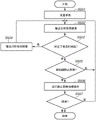
Fig. 5 is a flowchart illustrating a process according to an exemplary embodiment of the present invention.
Fig. 6 is a diagram illustrating a format of data output from an image sensor according to an exemplary embodiment of the present invention.
Fig. 7 is a diagram illustrating signal paths in an image processing unit according to an exemplary embodiment of the present invention.
Fig. 8A and 8B are timing charts each showing a case where the flicker detection mode is performed before a still image is captured according to an exemplary embodiment of the present invention.
Fig. 9 is a timing chart showing a case where Automatic Exposure (AE) detection is performed according to an exemplary embodiment of the present invention.
Detailed Description
Various exemplary embodiments of the present invention will be described in detail below with reference to the accompanying drawings. Fig. 1 is a block diagram showing an example of the structure of an image pickup apparatus according to an exemplary embodiment of the present invention. The image capturing apparatus 100 according to the present exemplary embodiment is, for example, a digital camera, and includes a still image capturing function and a moving image capturing function. In the still image photographing function, still image data in a Joint Photographic Experts Group (JPEG) format may be generated, and uncompressed still image data in an original format may be acquired. In the moving image shooting function, moving image data in 4K or 8K format can be acquired at a frame rate of 30 frames per second (fps) or more.
In fig. 1, a lens unit 101 forms an optical image of an object on an image sensor 105, and a lens driving apparatus 102 performs zoom control, focus control, and aperture control. The shutter control unit 104 mechanically controls the mechanical shutter 103 to control a light-shielding state with respect to the image sensor 105. The image sensor 105 converts an object image formed by the lens unit 101 into an image signal using a photoelectric conversion effect, and acquires the image signal. The image sensor 105 according to the present exemplary embodiment is a Complementary Metal Oxide Semiconductor (CMOS) type image sensor including a plurality of pixels in horizontal and vertical directions. The number of pixels included in the image sensor 105 is sufficient to acquire a moving image in 8K format. For example, the image sensor 105 includes 32000000 or more pixels. Each pixel may include a microlens for improving light collection efficiency, and a plurality of photoelectric conversion units.
The image processing unit 106 performs various types of correction on the image signal output from the image sensor 105. The image processing unit 106 according to the present exemplary embodiment performs defect correction, streak correction, and color correction on an image signal in addition to performing various types of image processing such as image synthesis processing, development processing, and compression/encoding processing on the image signal. The image processing unit 106 detects various types of information from the image signal corresponding to a single frame or a plurality of frames acquired from the image sensor 105. Examples of various types of information to be detected from an image include luminance information that specifies the brightness of the image, subject information relating to a subject contained in the image, and range information that specifies the distance to the subject. The image processing unit 106 according to the present exemplary embodiment is capable of detecting information about a light source in an image based on luminance information contained in a plurality of image signals.
The timing generation unit 107 is a driving unit configured to output various timing signals to the image sensor 105 and the image processing unit 106. Based on a clock from a predetermined clock source, the timing generation unit 107 generates a synchronization signal to be transmitted to the image sensor 105, and sets various operation parameters including drive mode setting to the image sensor 105 or the image processing unit 106 based on control of the control unit 109.
The control unit 109 controls various calculations and the entire image capturing apparatus 100, and includes a Central Processing Unit (CPU). The control unit 109 sets various setting parameters for each component. For example, the control unit 109 sets various parameters for driving via the timing generation unit 107 or directly to the image sensor 105, and supplies a timing signal including a periodic signal for controlling the output timing.
The control unit 109 executes a program recorded in the memory unit 108 to implement each process described below in the present exemplary embodiment. The control unit 109 includes a system memory, and uses, for example, a Random Access Memory (RAM) as the system memory. Constants and variables for operating the control unit 109 and a program read from the nonvolatile memory are loaded to the system memory. The nonvolatile memory is an electrically erasable and recordable memory, and a flash memory is used as the nonvolatile memory, for example. The nonvolatile memory may be configured to store constants for operating the control unit 109 and a program. The term "program" as used herein refers to a program for executing various types of control described below in the present exemplary embodiment. The control unit 109 may include a hardware circuit including a reconfigurable circuit in addition to a CPU for executing a program.
The memory unit 108 temporarily stores image data. The recording medium control I/F unit 110 is an interface for recording to the recording medium 111 or reading from the recording medium 111. The recording medium 111 is a removable recording medium such as a semiconductor memory or the like for recording or reading image data. The display unit 112 displays various types of information and captured images and a predetermined user interface. A touch panel may be provided on the display unit 112 as an operation unit (not shown) for receiving various operation instructions for the image capturing apparatus 100 from a user.
Next, an image capturing operation of the image capturing apparatus 100 having the above-described structure will be described below.
If the user operates a power switch of an operation unit (not shown), the main power is turned on or the standby state is released. As a result, power is supplied to the control unit 109, and also to circuits necessary for image capturing such as the image processing unit 106 and the image sensor 105.
After that, the image sensor 105 starts operating in the live view mode in synchronization with a predetermined synchronization signal based on the control of the control unit 109. The image data read in the live view mode is displayed on the display unit 112 in synchronization with a synchronization signal for display. During the operation in the live view mode, if a release switch of an operation unit (not shown) is operated, the control unit 109 controls the timing generation unit 107, and switches the image sensor 105 to the operation in the still image mode. If an image pickup operation in the still image mode is started, the image sensor 105 outputs signals from the corresponding pixels (all pixel rows in the effective area) as image data. The image data output from the image sensor 105 is subjected to correction calculation and image processing performed in the image processing unit 106, and is written in the memory unit 108 based on an instruction from the control unit 109. The data accumulated in the memory unit 108 is recorded to a removable recording medium 111 such as a semiconductor memory via a recording medium control I/F unit 110 based on the control of the control unit 109.
The image data may be directly or indirectly output to the computer via an external I/F unit (not shown).
(operation of image sensor)
The structure of the image sensor 105 according to the first exemplary embodiment will be described below with reference to fig. 2. Fig. 2 shows a circuit configuration of the image sensor 105. The image sensor 105 includes a pixel unit in which a plurality of unit pixels 202 are arranged in a matrix form (i.e., in the column direction and the row direction). The unit pixels 202 each include a photoelectric conversion element and a plurality of transistor elements configured to drive the photoelectric conversion element. The photoelectric conversion element converts incident light into an electrical signal using a photoelectric effect. The transistor elements of the unit pixels 202 are controlled by pixel control signals input from the vertical scanning circuit 201. Specifically, each row (pixel row) shares a horizontal signal line for supplying a control signal from the vertical scanning circuit 201 to each unit pixel 202, and the vertical scanning circuit 201 controls the unit pixels 202 mainly in row units by sequentially controlling row units each including a plurality of the unit pixels 202. For example, initialization of the photoelectric conversion element and reading of an electric signal from the unit pixel 202 are controlled by a row unit of the common horizontal signal line. Although the rows are configured to share the horizontal signal line for the purpose of simplifying the explanation in the present exemplary embodiment, the structure is not limited thereto. For example, two or more horizontal signal lines may be provided to each row and alternately connected to the unit pixels 202, or a plurality of rows may be configured to share the horizontal signal lines. Further, the unit pixels 202 each include a color filter of red, green, or blue and form a bayer arrangement.
The electric signal output from the unit pixel 202 is input to the column circuit 205 via the vertical signal line 204 formed in units of columns and including a plurality of unit pixels 202. The vertical signal line 204 is driven by a constant current source 203. The column circuit 205 includes: an amplifier circuit configured to amplify a signal; an analog/digital (AD) conversion circuit configured to convert an output from the unit pixel 202 into a digital signal; a memory configured to store the AD conversion result; and an addition/subtraction processing circuit configured to add/subtract an AD conversion result or a signal to be AD-converted. The digital signals processed by the column circuit 205 are sequentially output to the signal processing circuit 207 as image data in units of columns by the horizontal scanning circuit 206.
Although a structure in which one vertical signal line and one column circuit are provided to each pixel column is described here as an example, a plurality of vertical signal lines 204 and a plurality of column circuits 205 may be provided to each pixel column, and a plurality of rows may be read simultaneously. For example, in the case where 12 or more vertical signal lines 204 are provided to each column, image data of 12 rows is read by one reading operation. In the case of the structure including the plurality of vertical signal lines 204 as described above, a back-illuminated type or multilayer type structure that allows mounting of circuits on the opposite side of the light incident surface is desired. The signal processing circuit 207 includes a clamp processing unit configured to remove a component shifted by a dark current generated in the unit pixel 202. An interface for outputting image data to the image processing unit 106 as a subsequent-stage unit is desirably an interface employing a high-speed communication method using a differential pair, such as a low-voltage differential signaling (LVDS) method or an extended low-voltage signaling (SLVS) method. In the case of a structure including a plurality of channels as an interface for outputting image data, the respective channels may be configured to output signals different from each other.
Next, operations in the live view mode and the flicker detection mode will be described below with reference to fig. 3. Fig. 3 shows a part of the arrangement of the unit pixels 202 in the image sensor 105, and each index indicates the color (R: red, Gr/Gb: green, B: blue) of the color filter provided to each unit pixel 202. Fig. 3 shows an arrangement of the unit pixels 202, and indicates a row in which signals are to be read during operation in the live view mode and a row in which signals are to be read during operation in the flicker detection mode.
First, pixel rows to be read during operation in the live view mode will be described below. The live view operation refers to an operation of displaying an image on a rear liquid crystal display or an electronic viewfinder of the display unit 112 to provide an image for use by a user to determine an angle of view and image pickup conditions such as exposure conditions. In other words, such image data will not be stored in the recording medium 111, and since the number of pixels of the rear liquid crystal display is smaller than the number of unit pixels 202 of the image sensor 105, it is not necessary to read the image data from all the unit pixels 202. Generally, the number of pixels to be read is reduced to a number equal to or close to the number of pixels or lines of the rear liquid crystal display. For example, in the case where the number of effective pixels of the image sensor 105 is 8000 pixels in the horizontal direction and 5400 pixels in the vertical direction, reading image data of at least one-third of the number of pixels in the vertical direction is sufficient for obtaining a resolution corresponding to full high definition sufficient to display an image on the display unit 112. In the present exemplary embodiment, an example will be explained in which every third row (three-row cycle) of rows to be read is omitted. More specifically, in fig. 3, the following example will be explained: the number of pixels is reduced by omitting every third red line including the unit pixel 202 having the color filter R and every third blue line including the unit pixel 202 having the color filter B in the row direction. Further, an example in which two rows are added and one row is not read (one row is omitted) in a three-row period will be explained. Three line cycles and a reading method of adding and averaging two lines in three line cycles are merely examples. Other periods may also be used, for example, a period in which three of the five-row periods are added and averaged. Further, the addition method may be an operation of simply adding or an operation of adding and averaging. The method of adding the signals of two rows is intended to be, but not limited to, an addition and averaging method in which different rows are simultaneously connected to the vertical signal line 204.
Next, a pixel row to be read in the operation in the flicker detection mode will be described below. In the operation in the flicker detection mode, it is desirable to set lines to be read so as to achieve a frame rate of 600fps (≈ 1.66 milliseconds (msec)) or more. Thus, in the present exemplary embodiment, the image sensor 105 requires about 15msec to read the pixel rows of one frame, and is configured to read for every ninth red row and every ninth blue row (nine row periods) in the row direction (i.e., 15 msec/nine row period ═ 1.66 msec).
The pixel rows to be read in the operation in the flicker detection mode are pixel rows that are not read in the operation in the live view mode as shown in fig. 3. Since the pixel rows that are not read in the operation in the live view mode are used as described above, the live view mode and the flicker detection mode can be set at the same time. More specifically, this makes it possible to independently control the charge accumulation and reset operations in the respective modes. In the present exemplary embodiment, the electric signals respectively output from the subject pixel row in the operation in the live view mode and the subject pixel row in the operation in the flicker detection mode are processed using the common column circuit 205. Thus, the readout timing of the column circuit 205 is exclusively controlled.
Although the number of subject pixel rows in the operation in the live view mode and the operation in the flicker detection mode is shown in fig. 3, the number of pixels to be read may be set differently in the horizontal direction (pixel column). In one example, in operation in the live view mode, all pixels are read without omission or addition in the horizontal direction, and every third column is read in operation in the flicker detection mode. This structure improves the read rate in the operation in the flicker detection mode. In the case of prioritizing the processing load of the image processing unit 106, the number of subject pixel columns in the operation in the live view mode and the operation in the flicker detection mode may be set to the same number. Since the image processing unit 106 sequentially performs processing in units of pixel rows, if the number of pixels is the same in both modes, the same processing parameters can be used, whereby the processing load can be reduced.
Next, an example of an operation of simultaneously setting the live view mode and the flicker detection mode will be described below with reference to fig. 4. Fig. 4 shows an example of reading a live view image of one frame from the image sensor 105 at 30 fps. The image sensor 105 according to the present exemplary embodiment can read all pixel rows of one frame within about 15 msec. Thus, in the operation in the live view mode in which only one-third of the pixel lines are read, the image sensor 105 can acquire a live view image of one frame for about 5msec, and the remaining period (vertical blanking period) can be allocated to the operation in the flicker detection mode. Fig. 4 shows an example in which 12 images for flicker detection are read during a vertical blanking period while one live view image is read during one frame control signal period (hereinafter also referred to as a Vertical Drive (VD) period) corresponding to the frame rate. The operation sequence shown in fig. 4 makes it possible to perform an operation in the flicker detection mode without stopping the operation in the live view mode of the image sensor 105.
Specifically, in fig. 4, a frame control signal (hereinafter also referred to as VD) is a signal that is transmitted from the timing generation unit 107 and input to the image sensor 105, and specifies the timing to start a frame. In fig. 4, an example of reading a live view image at a frame rate of 30fps is shown. The flicker frequency of the flicker light source is set to 100 Hz. The operation of the slit scroll method is illustrated as an operation in each driving mode of the image sensor 105 in fig. 4. The reading operation from the unit pixel 202 is indicated by a solid line, and the reset operation is indicated by a broken line. Since the slit scroll operation is sequentially controlled in units of pixel rows, the lines are inclined. In fig. 4, the operation in the live view mode is represented by a thick line, and the operation in the flicker detection mode is represented by a thin line.
In fig. 4, at time t401, the VD is input to the image sensor 105, and a reading operation in the live view mode is started in synchronization with the VD. Then, at time t403, the reading operation of the first frame is started in the flicker detection mode. In the present exemplary embodiment, the time t403 is set to substantially the same timing as the timing at which the reading operation of the last pixel row in the live view mode ends. The reading operation in the flicker detection mode is started in synchronization with the timing at which the reading operation in the live view mode ends, whereby the number of times of reading in the flicker detection mode for each cycle is increased. Further, the length of time that the image sensor 105 operates is shortened, thereby saving power. Further, in a case where it is desired to increase the reading speed in the flicker detection mode, an operation to read the pixel lines only from a range smaller than the reading range in the live view mode may be performed.
The reading operation in the flicker detection mode is repeated until time t 405. In the present exemplary embodiment, a reading operation of reading 12 frames in the flicker detection mode is performed. The charge accumulation period (hereinafter referred to as accumulation period) in each mode is determined based on a predetermined exposure calculation result. For example, the accumulation period is determined using an immediately preceding frame or a number of preceding frames including the immediately preceding frame so that the subject is appropriately exposed. An image acquired by the operation in the flicker detection mode is used to detect flicker and is not displayed on the display unit 112. Thus, a shorter accumulation period than the accumulation period set to the operation in the live view mode can be set.
At time t403, the reading operation of the last pixel row in the live view mode and the start of the reading operation in the flicker detection mode are synchronized. Thus, at time t402 before the timing of the reading operation of the last pixel row in the live view mode, the reset operation corresponding to the reading operation in the flicker detection mode is performed.
The reset operation does not require the use of the column circuit 205, so that the read operation in the live view mode and the reset operation in the flicker detection mode can be set to overlap in time. Also, at time t404, a reset operation corresponding to the reading operation in the live view mode at time t406 is performed while the reading operation in the flicker detection mode is performed.
In the above-described example, while the operation in the live view mode is performed in the frame from the time t401, control is performed to drive the flicker detection mode a plurality of times. However, since it is unlikely that the type of light source (whether or not the light source is a flicker light source) for the subject changes within several tens of milliseconds, it is not necessary to constantly perform the flicker detection mode. The flicker detection mode may be performed at predetermined intervals, such as for every second or for every few seconds. Alternatively, the release switch may have a two-stage structure such that the flicker detection mode is performed in a case where the release switch is lightly pressed to the first stage, and the still image photographing is performed in a case where the release switch is deeply pressed to the second stage. During a period in which the operation in the flicker detection mode is not performed, it is desirable to control the column circuit 205 and the constant current source 203 to save power.
Processing of an image capturing operation performed by the image capturing apparatus 100 according to the present exemplary embodiment will be described below with reference to a flowchart shown in fig. 5. The control unit 109 performs each step.
First, in step S501, after the start of the image capturing operation, the control unit 109 sets various parameters to the image sensor 105 and the image processing unit 106 via the timing generation unit 107, and starts supplying the VD. The VD period of the VD supplied to the image sensor 105 corresponds to the frame rate at which the image sensor 105 operates, and in the present exemplary embodiment, the VD period is 1/30 sec. Then, the process advances to step S502. The various parameters include at least setting parameters of a driving mode in which the image sensor 105 operates and exposure parameters such as an accumulation period and a gain setting.
In step S502, the control unit 109 controls to start an operation in the live view mode in the image sensor 105 and cause the image sensor 105 to output image data. The output of the image data in the live view mode is repeatedly performed in synchronization with the VD supply timing. Then, the process advances to step S503.
In step S503, the control unit 109 measures the elapsed time based on the result of the time measurement by the time measurement unit (not shown). Then, the control unit 109 determines whether a predetermined period of time has elapsed. If the control unit 109 determines that the predetermined period of time has elapsed (yes in step S503), the processing proceeds to step S504. If the control unit 109 determines that the predetermined period of time has not elapsed (no in step S503), the processing proceeds to step S505. The timing at which the time measurement unit starts measurement or the reference of the time measurement is the previous flicker detection. More specifically, the control unit 109 determines whether a predetermined period of time has elapsed since the previous detection. At a time point immediately after the start of the flowchart, the probability that flicker detection is not performed until the time point is high, and thus the process may proceed to step S504 regardless of whether a predetermined period of time has elapsed. Although the determination is made based on the elapsed time in the present exemplary embodiment, the determination is not limited to the above determination. This determination may be made based on the number of output live view images or the number of VDs, for example.
In step S504, the control unit 109 controls to start an operation in the flicker detection mode in the image sensor 105, and causes the image sensor 105 to output image data for flicker detection. As shown in fig. 4, a plurality of image data for the flicker detection mode are output for one VD. Then, the process returns to step S502. To start the operation in the flicker detection mode, it is necessary to set parameters for setting the driving mode to the image sensor 105, but it is inconvenient to perform the setting for every several seconds. Thus, it is desirable to set a plurality of resistors for storing parameters for setting the driving mode to the image sensor 105 and to complete the setting of these resistors in step S501. Further, flags indicating which parameters for setting the driving mode are to be used may be set to these resistors, so that the operation of the image sensor 105 can be easily switched.
In step S505, the control unit 109 determines whether a still image shooting instruction is input based on a user operation of the release switch. If the control unit 109 determines that a still image shooting instruction is input (yes in step S505), the processing proceeds to step S506. If the control unit 109 determines that the still image shooting instruction is not input (no in step S505), the processing returns to step S502.
In step S506, the control unit 109 controls to start an operation in the still image mode in the image sensor 105 and cause the image sensor 105 to output image data. The output of the image data of the still image is performed only once in synchronization with the VD supply timing. Then, the process advances to step S507, and the process shown in the flowchart is repeated until an end instruction is received.
The flicker detection mode is performed in parallel with the operation in the live view mode within the vertical blanking period as described above, so that flicker detection can be performed without stopping the live view display.
Since the dark current is proportional to the accumulation period, the signal processing circuit 207 can be configured not to perform correction processing such as clamp processing or the like in a flicker detection mode in which a reset operation and a read operation are performed at high speed. In the present exemplary embodiment, an example is explained in which VD is not required in the flicker detection mode, and in this example, control for automatically switching the driving mode of the resistor provided to the image sensor 105 is required. In the case where the control load of this control is to be reduced, the VD for performing the flicker detection mode may be input alone.
Although the structure shown in fig. 2 includes one vertical signal line and column circuit 205 for each pixel column, a plurality of vertical signal lines and corresponding column circuits 205 may be provided. This structure allows the operation period in the live view mode and the operation period in the flicker detection mode to overlap, so that faster reading can be achieved.
(operation of image processing Unit)
Details of processing to be performed by the image processing unit 106 on the image data output from the image sensor 105 will be described below.
The operation of the signal processing circuit 207 provided to the image sensor 105 according to the present exemplary embodiment will be described below with reference to fig. 6. The signal processing circuit 207 includes a function of assigning an Identifier (ID) to the digital signal input from the column circuit 205, in addition to the above-described clamping processing. Fig. 6 shows an image of image data output from the image sensor 105 for VD. The output signal as the image data output from the image sensor 105 includes an ID and image data. The ID included in the output signal is also used by the image processing unit 106 as a subsequent stage unit. Since the image processing unit 106 performs processing in units of rows, it is desirable to assign IDs to each row as a processing unit. A plurality of bits are assigned to the ID.
In the present exemplary embodiment, the ID is used in determining the operation mode in which the image processing unit 106 acquires image data. More specifically, the ID is data different for each mode corresponding to the acquired image data. In the present exemplary embodiment, "a" refers to an ID assigned in the case of acquiring image data in an operation in the live view mode, and "B" refers to an ID assigned in the case of acquiring image data in an operation in the flicker detection mode.
In the case of a frame in which only the operation in the live view mode is performed within one VD period, image data having ID "a" is sequentially output to the image processing unit 106. In the case where frames of both the operation in the live view mode and the operation in the flicker detection mode are performed within one VD period as shown in fig. 4, the image data having the ID "B" is output after the image data having the ID "a". Although the operation in the flicker detection mode is performed after the end of the operation in the live view mode in the unit pixel reading in fig. 4, the reading is not limited to the above-described reading, and there may be a case where the operation period in the live view mode and the operation period in the flicker detection mode overlap. In this case, the pixel row or area contains both the image data with ID "a" and the image data with ID "B".
Next, the signal processing performed by the image processing unit 106 will be described below with reference to fig. 7. Fig. 7 shows a signal path of the image processing unit 106. The image processing unit 106 includes a signal path switching circuit 601, an image correction circuit 602, a development circuit 603, and a flicker detection circuit 604 on an input path from the image sensor 105. The signal path switching circuit 601 recognizes the ID of the input image data. Then, the signal path switching circuit 601 outputs the image data to one of a signal path (hereinafter, "image signal path") constituted by the image correction circuit 602 and the development circuit 603 and a signal path (hereinafter, "flicker detection signal path") constituted by the flicker detection circuit 604 at a subsequent stage. In the present exemplary embodiment, the image data having the ID "a" is output to the image signal path, and the image data having the ID "B" is output to the flicker detection signal path.
The image signal path is a path for generating an image to be displayed on the display unit 112 or an image to be recorded in the recording medium 111, and mainly the image correction circuit 602 performs various processes such as offset correction, gain correction, and color adjustment, followed by the development circuit 603 performing development processing. The image data subjected to the development processing is temporarily stored in the memory unit 108, and then displayed or recorded.
On the other hand, the flicker detection signal path is a path in which the flicker detection circuit 604 as a detection unit detects whether or not there is flicker based on luminance information on image data and calculates the cycle and phase of flicker. The detection or calculation result is output to the control unit 109. Then, the control unit 109 controls display of information on the presence or absence of flicker on the display unit 112 and controls the imaging control timing of the timing generation unit 107.
Although an example in which the operation in the live view mode and the operation in the flicker detection mode are performed in parallel within one VD period is shown in fig. 4, the configuration is not limited to the above example, and the operation in the flicker detection mode may also be performed within a plurality of VD periods. For example, in the case of performing an operation in the live view mode at 120fps, sometimes sufficient image data for flicker detection cannot be acquired within one VD period. In this case, it is desirable to make a setting to perform an operation in the flicker detection mode in a plurality of VD periods. In the case where the operation in the flicker detection mode is performed over a plurality of VD periods, the amount of image data acquired and output by the operation in the flicker detection mode may differ for each frame in addition to the image data acquired by the operation in the live view mode. Even if the amount of data becomes unequal between frames, since the image data is provided with the ID, the image data is appropriately guided in the image processing unit 106 without any special control.
As described above, the ID corresponding to the purpose is provided to the image data output from the image sensor 105, so that the image data continuously input in a very short period of time is efficiently guided to an appropriate signal path without the need for sequential setting.
In the first exemplary embodiment, an example has been described in which the operation in the flicker detection mode is performed within the vertical blanking period in the operation in the live view mode. In the second exemplary embodiment, an operation in the flicker detection mode in a case where the release switch is pressed and a still image photographing instruction is input while only the live view mode is operating will be described below.
In order to reduce the influence of the flickering light source, the image capturing apparatus 100 according to the present exemplary embodiment controls the accumulation start timing so that the center of the accumulation period during image capturing in the still image mode substantially coincides with the maximum value of the light amount variation of the light source. In the timing control, it is necessary to accurately detect the phase and light amount variation of flicker, so that it is desirable to perform an operation in the flicker detection mode immediately before an image capturing operation in the still image mode. However, in the case where the still image capturing operation is performed after the operation sequence of fig. 4 is performed, the release time lag between the input of the release signal and the start of accumulation may become long. In the present exemplary embodiment, a desirable sequence in the case where the release switch is pressed during the operation in the live view mode and the operation in the flicker detection mode is performed will be described.
Fig. 8A shows an example of the following case: the release switch is pressed during the operation in the live view mode, and the operation in the flicker detection mode is performed within the vertical blanking period in the operation in the live view mode that has been described above in the first exemplary embodiment. On the other hand, fig. 8B shows an example of a case where the operation in the flicker detection mode is independently performed in synchronization with the VD (independently of the operation in the live view mode). Although an example of control of controlling the accumulation period in the still image shooting operation using the shutter 103 is described in the present exemplary embodiment, the control is not limited to the above-described example, and the accumulation period may be controlled using an electronic shutter operation alone or in combination with a mechanical shutter operation.
First, fig. 8A will be explained below. At time t701a, VD is input, and reading in the live view mode is started. Next, at time t702a, in the case where the release switch is pressed, the timing generation unit 107 controls the image sensor 105 so that the operation in the flicker detection mode is performed within the vertical blanking period in the operation in the live view mode in the next frame.
Then, at a time t703a which is 33.3msec (═ 30fps) after the time t701a, if VD is input again, reading in the live view mode is performed again. Then, reading in the flicker detection mode is performed sequentially from time t704 a. Then, the flicker detection circuit 604 calculates the cycle and phase of flicker based on the image data for flicker detection repeatedly read during a predetermined period of time. For the still image photographing operation, the reset operation is performed for each pixel unit based on the VD input at time t705a after the end of the operation in the flicker detection mode. Then, at time t706a, the shutter 103 is controlled based on the cycle and phase of the detected flicker so that the center of the accumulation period substantially coincides with the maximum value of the light amount variation of the light source. After that, at time t707a, reading in the still image capturing operation is performed. In the operation shown in fig. 8A, there is a waiting time between the release switch being pressed and the VD being input for use in the operation in the live view mode. This is because the operation in the flicker detection mode is performed within the vertical blanking period in the operation in the live view mode. Although an operation in the flicker detection mode performed immediately before the still image capturing operation is realized, it is not desirable for a moving object.
Next, fig. 8B will be described below. At time t701b, VD is input, and live view reading is started. Next, at time t702b, in the case where the release switch is pressed, the timing generation unit 107 controls the image sensor 105 so that the operation in the flicker detection mode is performed in synchronization with VD in the next frame.
Then, at time t703b, when VD is input, an operation in the flicker detection mode is performed. Then, the flicker detection circuit 604 calculates the cycle and phase of flicker based on the image data for flicker detection repeatedly read within a predetermined period of time. For the still image photographing operation, the reset operation is performed for each pixel unit based on the VD input at time t704b after the operation in the flicker detection mode ends. Then, at time t705b, the shutter 103 is controlled based on the cycle and phase of the detected flicker so that the center of the accumulation period substantially coincides with the maximum value of the light amount variation of the light source. After that, at time t706b, reading in the still image capturing operation is performed.
The input of the VD at the time t703b is not synchronized with the VD at the time t701b, but is performed based on the release signal input at the time t702 b. Further, the input of the VD at the time t704b is performed after the elapse of the time period required for the operation in the flicker detection mode. For example, the VD is input after a period of time required to acquire 12 pieces of image data in the flicker detection mode has elapsed. As is apparent from fig. 4 or fig. 8A, the period required for the operation in the flicker detection mode is shorter than the VD period (33.3msec) in the operation in the live view mode, and the release time lag is shorter than that in fig. 8A. Thus, not only is an operation in the flicker detection mode performed immediately before the still image capturing operation achieved, but also a short release time lag is achieved, thereby reducing the risk of missing a good chance of capturing an image of a moving subject.
In the first exemplary embodiment and the second exemplary embodiment, it has been explained how the operation in the dedicated flicker detection mode is combined with the operation in another driving mode in order to detect the presence or absence of the flicker light source and the period and phase of the flicker. However, the light source for the subject may include a light source other than the flicker light source, and the characteristics of the other light sources may change.
In the third exemplary embodiment, a light source detection mode for detecting a characteristic of a light source for an object, which is not limited to a flicker light source, will be described below as another form of the flicker detection mode. In particular, an example will be described in which an increase in the dynamic range of luminance information is achieved in the case where Automatic Exposure (AE) processing is performed using luminance information on image data from the image sensor 105.
When detecting the characteristics of a light source for an object, it is important to detect how bright the light source is. For example, the brightness of a light source significantly differs depending on whether the light source is a solar light source or a fluorescent light source, and the imaging conditions for detecting the characteristics of the light source significantly differ. In the normal AE processing, the user can set an appropriate exposure without performing special control. However, in the case where the expected brightness of the light source is significantly different from the actual brightness of the light source, there is a possibility that the dynamic range determined based on the characteristics of the image sensor 105 is exceeded and accurate AE processing cannot be performed, and a good chance of capturing an image may be missed. Thus, in order to increase the speed of the AE processing for detecting the light source characteristics, it is desirable that the dynamic range of the image data from the image sensor 105 is increased.
Details of the driving mode of the image sensor 105 for increasing the dynamic range according to the present exemplary embodiment will be described below with reference to fig. 9. Fig. 9 shows the read operation timing in the case of acquiring luminance information having a wide dynamic range while performing an operation in the live view mode.
As a drive mode corresponding to the flicker detection mode in the present exemplary embodiment, a read operation for acquiring luminance information (hereinafter also referred to as AE information) for performing AE processing will be referred to as an AE detection mode. In the present exemplary embodiment, the lines to be read in the operation in the live view mode are the same as the lines to be read in the operation in the live view mode in fig. 3, and the lines to be read in the operation in the AE detection mode are the same as the lines to be read in the operation in the flicker detection mode in fig. 3. In the operation in the AE detection mode, reading at a high-speed frame rate is less necessary than in the operation in the flicker detection mode, and if a line that is not read in the operation in the live view mode is used, other lines may be used.
Fig. 9 shows an example of reading a live view image of one frame from the image sensor 105 at 30 fps. The image sensor 105 according to the present exemplary embodiment can read all pixel rows of one frame within about 15 msec. Thus, in the case of an operation in the live view mode in which only one-third of the pixel lines are to be read, a live view image of one frame is acquired for about 5msec, and the remaining period (vertical blanking period) can be allocated to the operation in the AE detection mode. In fig. 9, the following example is shown: two images for AE detection are read in the vertical blanking period while two live view images are read in two VD periods corresponding to the frame rate. The operation sequence shown in fig. 9 makes it possible to perform an operation in the AE detection mode without stopping an operation in the live view mode in the image sensor 105.
More specifically, in fig. 9, VD is a signal input from the timing generation unit 107 to the image sensor 105, and indicates a frame start timing. In the present exemplary embodiment, an example of reading a live view image at a frame rate of 30fps will be explained. The operation of the slit scroll method is shown as the operation in each driving mode of the image sensor 105 in fig. 9, and the reading operation from the unit pixel 202 is indicated by a solid line, and the reset operation is indicated by a broken line. The slit scroll operation is sequentially controlled in units of pixel rows such that each row is tilted. In fig. 9, the operation in the live view mode is represented by a thick line, and the operation in the AE detection mode is represented by a thin line.
In fig. 9, at time t801, the VD is input to the image sensor 105, and a reading operation in the live view mode is started in synchronization with the VD. Then, at time t804, the reading operation in the live view mode after accumulation for a predetermined period of time is performed again. Thereafter, at time t805, the first reading, which is a reading operation in the AE detection mode after accumulation for a predetermined accumulation period of time, is performed. At time t807, second reading, which is a reading operation in the AE detection mode after accumulation of an accumulation period shorter than the accumulation period corresponding to the first reading, is performed.
Since the reading operation in the live view mode and the reset operation in the flicker detection mode can overlap in time, the timing of the reset operation can be set more freely than the timing of the reading operation. In the present exemplary embodiment, at time t802, the first reset operation in the AE detection mode is performed. Next, at time t803, a reset operation in the live view mode is performed, and at time t806, a second reset operation in the AE detection mode is performed.
In the present exemplary embodiment, although the reading operation in the AE detection mode is performed twice in two VD periods, the number of times of the reading operation is not limited to two times, and may be three times or more. In this case, three or more accumulation periods may be set. Further, the reading in the AE detection mode may be performed once in one VD period. By controlling the first reading and the second reading as shown in fig. 9, the accumulation period corresponding to the first reading in the AE detection mode can be set to a period longer than one VD period. This makes it possible to increase the dynamic range while maintaining smooth live view display on the display unit 112.
Although in fig. 9 in the AE detection mode, a long-term accumulation period is set and a short-term accumulation period is set thereafter, these periods may be set in the reverse order. Further, although an example has been described in which a plurality of reading operations are performed in the AE detection mode, the AE detection mode may also be realized by performing one reading operation by providing an addition unit configured to add the reading operation results together in the image sensor 105.
Since the reading operation in the AE detection mode and the reading operation in the live view mode cannot be performed simultaneously, at time t805, the timing at which the reading in the live view mode ends and the timing at which the reading in the AE detection mode starts are set to substantially the same timing, but the timing is not limited to the above-described timing. For example, the reading operation in the AE detection mode and the reading operation in the live view mode may be performed at sufficiently separated timings, or in the case of a configuration including a plurality of vertical signal lines and corresponding column circuits 205, the operation period in the live view mode and the operation period in the flicker detection mode may be controlled to overlap.
In the present exemplary embodiment, an example has been described in which reading operations corresponding to a plurality of accumulation periods are performed to detect characteristics of a light source for an object. It is desirable to perform such a reading operation without knowing an appropriate exposure (for example, immediately after the start of image capturing or immediately after a change in an object, or immediately before a still image capturing operation that requires AE detection with high accuracy). Further, such reading operation may also be combined with the flicker detection mode described in the first and second exemplary embodiments, and an accumulation period longer than the other accumulation periods may be set by controlling one of the reset timings corresponding to the plurality of reading operations. Further, the characteristics of the light source that can be detected by applying the present exemplary embodiment and that can be set as a detection object include a change in luminance or color of the light source, an incident angle of the light source, a polarization state of the light source, and a waveform component of the light source.
The image capturing apparatus 100 described in each exemplary embodiment is applicable to various applications. For example, the image pickup apparatus 100 can be used to sense light such as infrared light, ultraviolet light, and X-rays in addition to visible light. The image capturing apparatus 100 is typically a digital camera, but is also applicable to camera-attached mobile phones such as smart phones, monitoring cameras, and game machines. The image pickup apparatus 100 is also applicable to an endoscope, a medical apparatus for taking an image of a blood vessel, a cosmetic device for observing the skin or scalp, and a camera for taking a moving image of a motion or action. The image pickup apparatus 100 is also applicable to a camera for traffic use such as a camera for monitoring traffic or a ship or an instrument panel camera, a camera for academic use such as astronomy or specimen observation, a home appliance to which the camera is attached, and machine vision. In particular, machine vision is not limited to industrial robots, and may also be applied in the agricultural and fishery fields.
The structure of the image pickup apparatus 100 described in the exemplary embodiment is merely an example, and the image pickup apparatus to which the present invention is applicable is not limited to the structure shown in fig. 1. Further, the circuit configuration of the components of the image pickup apparatus is not limited to the circuit configuration shown in the drawings.
The present invention can also be realized by the following processing: a program for implementing one or more functions of the above-described exemplary embodiments is supplied to a system or an apparatus via a network or a storage medium, and the one or more processors of the computer of the system or the apparatus read and execute the program. Furthermore, the invention may also be implemented by circuitry (e.g., an Application Specific Integrated Circuit (ASIC)) that performs one or more functions.
The above exemplary embodiments merely describe examples of specific implementations of the present invention, and the technical scope of the present invention should not be interpreted in a limiting manner by the specification. In other words, the present invention can be implemented in various forms without departing from the technical concept or main features of the present invention. The present invention provides an image pickup apparatus capable of flicker detection for detecting characteristics of a light source without stopping live view display.
OTHER EMBODIMENTS
The embodiments of the present invention can also be realized by a method in which software (programs) that perform the functions of the above-described embodiments are supplied to a system or an apparatus through a network or various storage media, and a computer or a Central Processing Unit (CPU), a Micro Processing Unit (MPU) of the system or the apparatus reads out and executes the methods of the programs.
While the present invention has been described with reference to exemplary embodiments, it is to be understood that the invention is not limited to the disclosed exemplary embodiments. The scope of the following claims is to be accorded the broadest interpretation so as to encompass all such modifications and equivalent structures and functions.
Claims (6)
1. An image pickup apparatus includes:
a sensor including a pixel unit in which a plurality of unit pixels each including a photoelectric conversion element are arranged in a column direction and a row direction;
a processing unit configured to assign a first identifier, i.e., a first ID, to first image data based on signals read out from a plurality of first pixel rows of the pixel unit, and assign a second identifier, i.e., a second ID, to second image data based on signals read out from a plurality of second pixel rows of the pixel unit, which are different from the plurality of first pixel rows;
an image correction circuit configured to perform predetermined correction processing on image data output from the pixel unit;
a development circuit configured to perform development processing on the image data on which the predetermined correction processing has been performed by the image correction circuit;
a flicker detection circuit configured to detect whether flicker is present; and
a signal path switching circuit configured to receive an input of the image data, perform ID recognition on the input image data, output the first image data to which the first ID is assigned to the image correction circuit, and output the second image data to which the second ID is assigned to the flicker detection circuit.
2. The image pickup apparatus according to claim 1, further comprising:
a display unit configured to display an image based on the first image data.
3. The image capturing apparatus according to claim 2, wherein the second image data is not displayed on the display unit.
4. The image pickup apparatus according to any one of claims 1 to 3, wherein reading of signals from the plurality of second pixel rows of the pixel unit is performed after reading of signals from the plurality of first pixel rows of the pixel unit.
5. The image capturing apparatus according to claim 4, wherein the accumulation period in the plurality of first pixel rows and the accumulation period in the plurality of second pixel rows at least partially overlap.
6. The image pickup apparatus according to any one of claims 1 to 3, wherein exposure conditions in the plurality of first pixel rows and exposure conditions in the plurality of second pixel rows are individually controllable.
Applications Claiming Priority (2)
| Application Number | Priority Date | Filing Date | Title |
|---|---|---|---|
| JP2018-213730 | 2018-11-14 | ||
| JP2018213730A JP7278750B2 (en) | 2018-11-14 | 2018-11-14 | Imaging device |
Publications (2)
| Publication Number | Publication Date |
|---|---|
| CN111193846A CN111193846A (en) | 2020-05-22 |
| CN111193846B true CN111193846B (en) | 2022-03-29 |
Family
ID=70550942
Family Applications (1)
| Application Number | Title | Priority Date | Filing Date |
|---|---|---|---|
| CN201911112591.0A Active CN111193846B (en) | 2018-11-14 | 2019-11-14 | Image pickup apparatus |
Country Status (3)
| Country | Link |
|---|---|
| US (1) | US11184554B2 (en) |
| JP (1) | JP7278750B2 (en) |
| CN (1) | CN111193846B (en) |
Families Citing this family (4)
| Publication number | Priority date | Publication date | Assignee | Title |
|---|---|---|---|---|
| JP2022128228A (en) | 2021-02-22 | 2022-09-01 | キヤノン株式会社 | Imaging device and control method thereof, program, and storage medium |
| JP2022165817A (en) | 2021-04-20 | 2022-11-01 | キヤノン株式会社 | Imaging apparatus and control method for the same, program, and storage medium |
| JP2022170437A (en) | 2021-04-28 | 2022-11-10 | キヤノン株式会社 | Electronic apparatus and control method therefor |
| WO2023004620A1 (en) * | 2021-07-28 | 2023-02-02 | 华为技术有限公司 | Data reading apparatus and related method |
Citations (1)
| Publication number | Priority date | Publication date | Assignee | Title |
|---|---|---|---|---|
| CN104364673A (en) * | 2012-05-29 | 2015-02-18 | 布莱特瓦维森有限公司 | Gated imaging using an adaptive depth of field |
Family Cites Families (11)
| Publication number | Priority date | Publication date | Assignee | Title |
|---|---|---|---|---|
| KR100371428B1 (en) * | 1995-03-28 | 2003-04-08 | 마츠시타 덴끼 산교 가부시키가이샤 | Image recording apparatus and image reproducing apparatus |
| JP2006287362A (en) * | 2005-03-31 | 2006-10-19 | Eastman Kodak Co | Digital camera and white balance adjustment method |
| JP4377840B2 (en) | 2005-03-31 | 2009-12-02 | イーストマン コダック カンパニー | Digital camera |
| US9077917B2 (en) * | 2011-06-09 | 2015-07-07 | Apple Inc. | Image sensor having HDR capture capability |
| EP2713608B1 (en) * | 2012-10-01 | 2015-04-29 | Axis AB | A device and a method for image acquisition |
| KR20140109668A (en) * | 2013-03-06 | 2014-09-16 | 삼성전자주식회사 | Method and system for detecting flicker |
| US9473706B2 (en) | 2013-12-09 | 2016-10-18 | Apple Inc. | Image sensor flicker detection |
| JP2015115922A (en) | 2013-12-16 | 2015-06-22 | オリンパス株式会社 | Imaging apparatus and imaging method |
| JP6525757B2 (en) | 2015-06-17 | 2019-06-05 | キヤノン株式会社 | Image pickup apparatus, method of calculating light quantity change characteristics, program, and storage medium |
| JP2018033072A (en) | 2016-08-26 | 2018-03-01 | ソニーセミコンダクタソリューションズ株式会社 | Imaging apparatus, imaging system, and signal processing method |
| JP6845173B2 (en) * | 2018-03-15 | 2021-03-17 | 株式会社東芝 | Image processing device and image processing method |
-
2018
- 2018-11-14 JP JP2018213730A patent/JP7278750B2/en active Active
-
2019
- 2019-11-06 US US16/676,265 patent/US11184554B2/en active Active
- 2019-11-14 CN CN201911112591.0A patent/CN111193846B/en active Active
Patent Citations (1)
| Publication number | Priority date | Publication date | Assignee | Title |
|---|---|---|---|---|
| CN104364673A (en) * | 2012-05-29 | 2015-02-18 | 布莱特瓦维森有限公司 | Gated imaging using an adaptive depth of field |
Also Published As
| Publication number | Publication date |
|---|---|
| US20200154031A1 (en) | 2020-05-14 |
| JP2020080512A (en) | 2020-05-28 |
| CN111193846A (en) | 2020-05-22 |
| US11184554B2 (en) | 2021-11-23 |
| JP7278750B2 (en) | 2023-05-22 |
Similar Documents
| Publication | Publication Date | Title |
|---|---|---|
| CN111193846B (en) | Image pickup apparatus | |
| JP5523124B2 (en) | Imaging device | |
| EP2793457A1 (en) | Image processing device, image processing method, and recording medium | |
| JP2010114834A (en) | Imaging apparatus | |
| KR101044647B1 (en) | Imaging device | |
| JP2011103550A (en) | Device and method for sensing image | |
| US20130050455A1 (en) | Endoscope apparatus | |
| JP5221722B2 (en) | Imaging apparatus and endoscope apparatus | |
| JPH1051796A (en) | Solid-state image pickup device | |
| JP5484617B2 (en) | Imaging device | |
| US8866948B2 (en) | Imaging apparatus | |
| JP5279638B2 (en) | Imaging device | |
| JP2009272813A (en) | Imaging apparatus, and image display method | |
| JP5581968B2 (en) | Imaging device | |
| JP5440245B2 (en) | Imaging device | |
| US20180176445A1 (en) | Imaging device and imaging method | |
| JP2010171930A (en) | Imaging apparatus and imaging method | |
| JP6924089B2 (en) | Imaging device and its control method | |
| JP2016096551A (en) | Imaging device | |
| JP2017108336A (en) | Imaging apparatus, control method therefor, and control program | |
| JP5630132B2 (en) | Imaging device | |
| CN106937065B (en) | Video display method, system and endoscope device comprising video display system | |
| JP2018050346A (en) | Imaging apparatus | |
| CN111728578B (en) | Capsule endoscope control method and capsule endoscope | |
| JP4439245B2 (en) | Electronic endoscope device |
Legal Events
| Date | Code | Title | Description |
|---|---|---|---|
| PB01 | Publication | ||
| PB01 | Publication | ||
| SE01 | Entry into force of request for substantive examination | ||
| SE01 | Entry into force of request for substantive examination | ||
| GR01 | Patent grant | ||
| GR01 | Patent grant |