CN111031663B - Copper foil substrate - Google Patents
Copper foil substrate Download PDFInfo
- Publication number
- CN111031663B CN111031663B CN201811173307.6A CN201811173307A CN111031663B CN 111031663 B CN111031663 B CN 111031663B CN 201811173307 A CN201811173307 A CN 201811173307A CN 111031663 B CN111031663 B CN 111031663B
- Authority
- CN
- China
- Prior art keywords
- copper foil
- micro
- microns
- less
- equal
- Prior art date
- Legal status (The legal status is an assumption and is not a legal conclusion. Google has not performed a legal analysis and makes no representation as to the accuracy of the status listed.)
- Active
Links
- RYGMFSIKBFXOCR-UHFFFAOYSA-N Copper Chemical compound [Cu] RYGMFSIKBFXOCR-UHFFFAOYSA-N 0.000 title claims abstract description 126
- 239000011889 copper foil Substances 0.000 title claims abstract description 104
- 239000000758 substrate Substances 0.000 title claims abstract description 66
- 238000003780 insertion Methods 0.000 claims abstract description 34
- 230000037431 insertion Effects 0.000 claims abstract description 34
- 239000013081 microcrystal Substances 0.000 claims abstract description 34
- 239000013078 crystal Substances 0.000 claims description 4
- 229910052802 copper Inorganic materials 0.000 description 22
- 239000010949 copper Substances 0.000 description 22
- 238000007747 plating Methods 0.000 description 19
- 238000007788 roughening Methods 0.000 description 15
- 238000004519 manufacturing process Methods 0.000 description 13
- 238000011282 treatment Methods 0.000 description 13
- 238000000034 method Methods 0.000 description 9
- 239000011888 foil Substances 0.000 description 8
- 230000000052 comparative effect Effects 0.000 description 7
- 239000000463 material Substances 0.000 description 7
- 238000012360 testing method Methods 0.000 description 7
- 238000005868 electrolysis reaction Methods 0.000 description 6
- 230000008054 signal transmission Effects 0.000 description 6
- JPVYNHNXODAKFH-UHFFFAOYSA-N Cu2+ Chemical compound [Cu+2] JPVYNHNXODAKFH-UHFFFAOYSA-N 0.000 description 5
- 239000000654 additive Substances 0.000 description 5
- 229910001431 copper ion Inorganic materials 0.000 description 5
- 229910052751 metal Inorganic materials 0.000 description 5
- 239000002184 metal Substances 0.000 description 5
- 239000011347 resin Substances 0.000 description 5
- 229920005989 resin Polymers 0.000 description 5
- 239000002253 acid Substances 0.000 description 4
- BASFCYQUMIYNBI-UHFFFAOYSA-N platinum Chemical compound [Pt] BASFCYQUMIYNBI-UHFFFAOYSA-N 0.000 description 4
- 229920000663 Hydroxyethyl cellulose Polymers 0.000 description 3
- 238000009713 electroplating Methods 0.000 description 3
- 239000011521 glass Substances 0.000 description 3
- 238000001000 micrograph Methods 0.000 description 3
- 229920001223 polyethylene glycol Polymers 0.000 description 3
- 229920003002 synthetic resin Polymers 0.000 description 3
- 239000000057 synthetic resin Substances 0.000 description 3
- 239000004354 Hydroxyethyl cellulose Substances 0.000 description 2
- XEEYBQQBJWHFJM-UHFFFAOYSA-N Iron Chemical compound [Fe] XEEYBQQBJWHFJM-UHFFFAOYSA-N 0.000 description 2
- -1 Poly(ethylene glycol) Polymers 0.000 description 2
- QAOWNCQODCNURD-UHFFFAOYSA-N Sulfuric acid Chemical compound OS(O)(=O)=O QAOWNCQODCNURD-UHFFFAOYSA-N 0.000 description 2
- 230000009286 beneficial effect Effects 0.000 description 2
- 229910000365 copper sulfate Inorganic materials 0.000 description 2
- ARUVKPQLZAKDPS-UHFFFAOYSA-L copper(II) sulfate Chemical compound [Cu+2].[O-][S+2]([O-])([O-])[O-] ARUVKPQLZAKDPS-UHFFFAOYSA-L 0.000 description 2
- 230000000694 effects Effects 0.000 description 2
- 239000000835 fiber Substances 0.000 description 2
- 235000019447 hydroxyethyl cellulose Nutrition 0.000 description 2
- 238000010030 laminating Methods 0.000 description 2
- 239000010410 layer Substances 0.000 description 2
- 238000000691 measurement method Methods 0.000 description 2
- 239000004745 nonwoven fabric Substances 0.000 description 2
- 239000002245 particle Substances 0.000 description 2
- 229910052697 platinum Inorganic materials 0.000 description 2
- 239000000047 product Substances 0.000 description 2
- 230000003746 surface roughness Effects 0.000 description 2
- JYEUMXHLPRZUAT-UHFFFAOYSA-N 1,2,3-triazine Chemical compound C1=CN=NN=C1 JYEUMXHLPRZUAT-UHFFFAOYSA-N 0.000 description 1
- XQUPVDVFXZDTLT-UHFFFAOYSA-N 1-[4-[[4-(2,5-dioxopyrrol-1-yl)phenyl]methyl]phenyl]pyrrole-2,5-dione Chemical compound O=C1C=CC(=O)N1C(C=C1)=CC=C1CC1=CC=C(N2C(C=CC2=O)=O)C=C1 XQUPVDVFXZDTLT-UHFFFAOYSA-N 0.000 description 1
- 108010010803 Gelatin Proteins 0.000 description 1
- DGAQECJNVWCQMB-PUAWFVPOSA-M Ilexoside XXIX Chemical compound C[C@@H]1CC[C@@]2(CC[C@@]3(C(=CC[C@H]4[C@]3(CC[C@@H]5[C@@]4(CC[C@@H](C5(C)C)OS(=O)(=O)[O-])C)C)[C@@H]2[C@]1(C)O)C)C(=O)O[C@H]6[C@@H]([C@H]([C@@H]([C@H](O6)CO)O)O)O.[Na+] DGAQECJNVWCQMB-PUAWFVPOSA-M 0.000 description 1
- GRYLNZFGIOXLOG-UHFFFAOYSA-N Nitric acid Chemical compound O[N+]([O-])=O GRYLNZFGIOXLOG-UHFFFAOYSA-N 0.000 description 1
- 239000002202 Polyethylene glycol Substances 0.000 description 1
- 239000006087 Silane Coupling Agent Substances 0.000 description 1
- 229910000831 Steel Inorganic materials 0.000 description 1
- HCHKCACWOHOZIP-UHFFFAOYSA-N Zinc Chemical compound [Zn] HCHKCACWOHOZIP-UHFFFAOYSA-N 0.000 description 1
- 150000007513 acids Chemical class 0.000 description 1
- 230000000996 additive effect Effects 0.000 description 1
- 239000000853 adhesive Substances 0.000 description 1
- 230000001070 adhesive effect Effects 0.000 description 1
- 239000007795 chemical reaction product Substances 0.000 description 1
- 229910017052 cobalt Inorganic materials 0.000 description 1
- 239000010941 cobalt Substances 0.000 description 1
- GUTLYIVDDKVIGB-UHFFFAOYSA-N cobalt atom Chemical compound [Co] GUTLYIVDDKVIGB-UHFFFAOYSA-N 0.000 description 1
- 239000002131 composite material Substances 0.000 description 1
- LQCKYENTJVICBF-UHFFFAOYSA-N copper silane Chemical compound [SiH4].[Cu] LQCKYENTJVICBF-UHFFFAOYSA-N 0.000 description 1
- XTVVROIMIGLXTD-UHFFFAOYSA-N copper(II) nitrate Chemical compound [Cu+2].[O-][N+]([O-])=O.[O-][N+]([O-])=O XTVVROIMIGLXTD-UHFFFAOYSA-N 0.000 description 1
- XLJMAIOERFSOGZ-UHFFFAOYSA-M cyanate Chemical compound [O-]C#N XLJMAIOERFSOGZ-UHFFFAOYSA-M 0.000 description 1
- 230000007812 deficiency Effects 0.000 description 1
- 238000013461 design Methods 0.000 description 1
- 238000001514 detection method Methods 0.000 description 1
- 238000011161 development Methods 0.000 description 1
- 238000010586 diagram Methods 0.000 description 1
- WIYCQLLGDNXIBA-UHFFFAOYSA-L disodium;3-(3-sulfonatopropyldisulfanyl)propane-1-sulfonate Chemical compound [Na+].[Na+].[O-]S(=O)(=O)CCCSSCCCS([O-])(=O)=O WIYCQLLGDNXIBA-UHFFFAOYSA-L 0.000 description 1
- 239000003822 epoxy resin Substances 0.000 description 1
- 239000004744 fabric Substances 0.000 description 1
- 229920000159 gelatin Polymers 0.000 description 1
- 239000008273 gelatin Substances 0.000 description 1
- 235000019322 gelatine Nutrition 0.000 description 1
- 235000011852 gelatine desserts Nutrition 0.000 description 1
- 229910052742 iron Inorganic materials 0.000 description 1
- 150000002739 metals Chemical class 0.000 description 1
- 239000000203 mixture Substances 0.000 description 1
- 238000012986 modification Methods 0.000 description 1
- 230000004048 modification Effects 0.000 description 1
- 229910017604 nitric acid Inorganic materials 0.000 description 1
- 150000002897 organic nitrogen compounds Chemical class 0.000 description 1
- ISWSIDIOOBJBQZ-UHFFFAOYSA-N phenol group Chemical group C1(=CC=CC=C1)O ISWSIDIOOBJBQZ-UHFFFAOYSA-N 0.000 description 1
- 239000005011 phenolic resin Substances 0.000 description 1
- 229920003192 poly(bis maleimide) Polymers 0.000 description 1
- 229920000647 polyepoxide Polymers 0.000 description 1
- 229920001225 polyester resin Polymers 0.000 description 1
- 239000004645 polyester resin Substances 0.000 description 1
- 229920001721 polyimide Polymers 0.000 description 1
- 239000009719 polyimide resin Substances 0.000 description 1
- 229920001955 polyphenylene ether Polymers 0.000 description 1
- 238000001878 scanning electron micrograph Methods 0.000 description 1
- 239000002356 single layer Substances 0.000 description 1
- 229910052708 sodium Inorganic materials 0.000 description 1
- 239000011734 sodium Substances 0.000 description 1
- 239000010959 steel Substances 0.000 description 1
- BDHFUVZGWQCTTF-UHFFFAOYSA-M sulfonate Chemical compound [O-]S(=O)=O BDHFUVZGWQCTTF-UHFFFAOYSA-M 0.000 description 1
- 238000010998 test method Methods 0.000 description 1
- 150000003585 thioureas Chemical class 0.000 description 1
- 239000002759 woven fabric Substances 0.000 description 1
- 229910052725 zinc Inorganic materials 0.000 description 1
- 239000011701 zinc Substances 0.000 description 1
Images


Classifications
-
- H—ELECTRICITY
- H05—ELECTRIC TECHNIQUES NOT OTHERWISE PROVIDED FOR
- H05K—PRINTED CIRCUITS; CASINGS OR CONSTRUCTIONAL DETAILS OF ELECTRIC APPARATUS; MANUFACTURE OF ASSEMBLAGES OF ELECTRICAL COMPONENTS
- H05K1/00—Printed circuits
- H05K1/02—Details
- H05K1/09—Use of materials for the conductive, e.g. metallic pattern
-
- C—CHEMISTRY; METALLURGY
- C25—ELECTROLYTIC OR ELECTROPHORETIC PROCESSES; APPARATUS THEREFOR
- C25F—PROCESSES FOR THE ELECTROLYTIC REMOVAL OF MATERIALS FROM OBJECTS; APPARATUS THEREFOR
- C25F3/00—Electrolytic etching or polishing
- C25F3/02—Etching
-
- H—ELECTRICITY
- H05—ELECTRIC TECHNIQUES NOT OTHERWISE PROVIDED FOR
- H05K—PRINTED CIRCUITS; CASINGS OR CONSTRUCTIONAL DETAILS OF ELECTRIC APPARATUS; MANUFACTURE OF ASSEMBLAGES OF ELECTRICAL COMPONENTS
- H05K2201/00—Indexing scheme relating to printed circuits covered by H05K1/00
- H05K2201/03—Conductive materials
- H05K2201/0332—Structure of the conductor
- H05K2201/0335—Layered conductors or foils
- H05K2201/0355—Metal foils
-
- H—ELECTRICITY
- H05—ELECTRIC TECHNIQUES NOT OTHERWISE PROVIDED FOR
- H05K—PRINTED CIRCUITS; CASINGS OR CONSTRUCTIONAL DETAILS OF ELECTRIC APPARATUS; MANUFACTURE OF ASSEMBLAGES OF ELECTRICAL COMPONENTS
- H05K2201/00—Indexing scheme relating to printed circuits covered by H05K1/00
- H05K2201/03—Conductive materials
- H05K2201/0332—Structure of the conductor
- H05K2201/0364—Conductor shape
- H05K2201/0373—Conductors having a fine structure, e.g. providing a plurality of contact points with a structured tool
Landscapes
- Engineering & Computer Science (AREA)
- Chemical & Material Sciences (AREA)
- Microelectronics & Electronic Packaging (AREA)
- Chemical Kinetics & Catalysis (AREA)
- Electrochemistry (AREA)
- Materials Engineering (AREA)
- Metallurgy (AREA)
- Organic Chemistry (AREA)
- Electroplating Methods And Accessories (AREA)
Abstract
Description
技术领域technical field
本发明涉及一种铜箔,特别是涉及一种电解铜箔及具有此铜箔的铜箔基板。The invention relates to a copper foil, in particular to an electrolytic copper foil and a copper foil substrate with the copper foil.
背景技术Background technique
随着信息和电子产业的发展,高频高速的讯号传输已成为现代电路设计与制造的一环。电子产品为了能符合高频高速的讯号传输需求,所采用的铜箔基板在高频下需要有良好的介入损失(insertion loss)表现,以防止高频讯号在传递时产生过度的损耗。铜箔基板的介入损失与其表面粗糙度有高度关联。当表面粗糙度降低时,介入损失有较佳的表现,反之则否。但是降低粗糙度的同时,也会导致铜箔与基材间的剥离强度下滑,影响到后端产品的良率。因此,如何将剥离强度维持在业界水平,并提供良好的介入损失表现,已成为本领域所欲解决的课题。With the development of information and electronics industry, high-frequency and high-speed signal transmission has become a part of modern circuit design and manufacture. In order to meet the high-frequency and high-speed signal transmission requirements of electronic products, the copper foil substrate used must have good insertion loss performance at high frequencies to prevent excessive loss during high-frequency signal transmission. The insertion loss of copper clad substrate is highly related to its surface roughness. When the surface roughness is reduced, the insertion loss has a better performance, and vice versa. However, while reducing the roughness, it will also lead to a decrease in the peel strength between the copper foil and the substrate, which will affect the yield of the back-end products. Therefore, how to maintain the peel strength at the industry level and provide good insertion loss performance has become a problem to be solved in this field.
发明内容Contents of the invention
本发明所要解决的技术问题在于,针对现有技术的不足提供一种微粗糙电解铜箔。The technical problem to be solved by the present invention is to provide a micro-rough electrolytic copper foil for the deficiencies of the prior art.
为了解决上述的技术问题,本发明所采用的其中一技术方案是,提供一种微粗糙电解铜箔。所述微粗糙电解铜箔包括一微粗糙表面。所述微粗糙表面具有多个凸峰、多个凹槽以及多个微结晶簇。所述凹槽具有U形剖面轮廓及/或V形剖面轮廓,所述凹槽的平均宽度介于0.1至4微米,所述凹槽的平均深度小于或等于1.5微米。所述微结晶簇位于所述凸峰顶部。每一个所述微结晶簇由多个平均直径小于或等于0.5微米的微结晶堆栈构成。所述微粗糙电解铜箔的微粗糙表面的Rlr值低于1.3。In order to solve the above technical problems, one of the technical solutions adopted by the present invention is to provide a micro-roughened electrolytic copper foil. The micro-rough electrolytic copper foil includes a micro-rough surface. The micro-rough surface has a plurality of convex peaks, a plurality of grooves and a plurality of microcrystalline clusters. The groove has a U-shaped cross-sectional profile and/or a V-shaped cross-sectional profile, the average width of the groove is between 0.1 and 4 microns, and the average depth of the groove is less than or equal to 1.5 microns. The microcrystalline clusters are located on top of the convex peaks. Each microcrystalline cluster is composed of a plurality of microcrystalline stacks with an average diameter less than or equal to 0.5 microns. The Rlr value of the micro-rough surface of the micro-rough electrolytic copper foil is lower than 1.3.
优选地,每一个所述微结晶簇由多个微结晶堆栈构成,所述微结晶的平均直径小于或等于0.5微米,每一个所述微结晶簇的平均高度小于或等于2微米。Preferably, each microcrystal cluster is composed of a plurality of microcrystal stacks, the average diameter of the microcrystals is less than or equal to 0.5 microns, and the average height of each microcrystal cluster is less than or equal to 2 microns.
优选地,每一个所述微结晶簇由多个微结晶堆栈构成,所述微结晶的平均直径小于或等于0.5微米,每一个所述微结晶簇的平均高度小于或等于1.3微米。多个所述微结晶构成一分岔状的结晶团。Preferably, each microcrystal cluster is composed of a plurality of microcrystal stacks, the average diameter of the microcrystals is less than or equal to 0.5 microns, and the average height of each microcrystal cluster is less than or equal to 1.3 microns. A plurality of microcrystals form a branched crystal group.
优选地,所述微粗糙电解铜箔的微粗糙表面的Rlr值低于1.26。Preferably, the Rlr value of the micro-rough surface of the micro-rough electrolytic copper foil is lower than 1.26.
为了解决上述的技术问题,本发明所采用的其中一技术方案是,提供一种铜箔基板,其包括一基材以及一微粗糙电解铜箔。所述微粗糙电解铜箔包括一贴附在所述基材的微粗糙表面,所述微粗糙表面形成有多个凸峰、多个凹槽以及多个微结晶簇,所述凹槽的平均宽度介于0.1至4微米,所述凹槽的平均深度小于或等于1.5微米,所述微结晶簇位于所述凸峰顶部,所述微结晶簇的平均高度小于或等于2微米。所述铜箔基板于20GHz的介入损失(Insertion Loss)介于0至-1.5db/in。所述微粗糙电解铜箔与所述基材间的剥离强度大于4.3lb/in。In order to solve the above technical problems, one of the technical solutions adopted by the present invention is to provide a copper foil substrate, which includes a base material and a micro-rough electrolytic copper foil. The micro-rough electrolytic copper foil includes a micro-rough surface attached to the substrate, the micro-rough surface is formed with a plurality of convex peaks, a plurality of grooves and a plurality of micro-crystal clusters, the average of the grooves The width is between 0.1 and 4 microns, the average depth of the grooves is less than or equal to 1.5 microns, the microcrystalline clusters are located on the top of the convex peaks, and the average height of the microcrystalline clusters is less than or equal to 2 microns. The insertion loss of the copper foil substrate at 20 GHz is between 0 and -1.5 db/in. The peeling strength between the microrough electrolytic copper foil and the substrate is greater than 4.3 lb/in.
优选地,所述铜箔基板于16GHz的介入损失介于0至-1.2db/in。Preferably, the insertion loss of the copper foil substrate at 16 GHz is between 0 and -1.2 db/in.
优选地,所述铜箔基板于8GHz的介入损失介于0至-0.65db/in,所述铜箔基板于12.89GHz的介入损失介于0至-1.0db/in。Preferably, the insertion loss of the copper foil substrate at 8 GHz is between 0 and -0.65 db/in, and the insertion loss of the copper foil substrate at 12.89 GHz is between 0 and -1.0 db/in.
优选地,所述铜箔基板于8GHz的介入损失介于0至-0.63db/in,所述铜箔基板于12.89GHz的介入损失介于0至-0.97db/in,所述铜箔基板于16GHz的介入损失介于0至-1.15db/in,所述铜箔基板于20GHz的介入损失介于0至-1.45db/in。Preferably, the insertion loss of the copper foil substrate at 8GHz is between 0 and -0.63db/in, and the insertion loss of the copper foil substrate at 12.89GHz is between 0 and -0.97db/in. The insertion loss at 16GHz is between 0 and -1.15db/in, and the insertion loss of the copper foil substrate at 20GHz is between 0 and -1.45db/in.
优选地,所述微结晶簇的平均最大宽度小于或等于5微米;部份的所述微结晶簇形成有分岔结构;每一个所述微结晶簇的平均高度小于或等于1.8微米;每一个所述微结晶簇由多个微结晶堆栈构成,所述微结晶的平均直径小于或等于0.5微米;所述微粗糙电解铜箔的微粗糙表面的Rlr值低于1.26。Preferably, the average maximum width of the microcrystalline clusters is less than or equal to 5 microns; part of the microcrystalline clusters form a bifurcated structure; the average height of each of the microcrystalline clusters is less than or equal to 1.8 microns; each The microcrystal cluster is composed of multiple microcrystal stacks, and the average diameter of the microcrystals is less than or equal to 0.5 microns; the Rlr value of the microrough surface of the microrough electrolytic copper foil is lower than 1.26.
优选地,所述基材在在10GHz频率下的Dk值小于或等于4且在10GHz频率下的Df值小于或等于0.020,更佳地,所述基材11在10GHz频率下的Dk值小于或等于3.8且在10GHz频率下的Df值小于或等于0.015。Preferably, the Dk value of the substrate at a frequency of 10 GHz is less than or equal to 4 and the Df value at a frequency of 10 GHz is less than or equal to 0.020, more preferably, the Dk value of the substrate 11 at a frequency of 10 GHz is less than or equal to Equal to 3.8 and the Df value at 10GHz frequency is less than or equal to 0.015.
本发明的其中一有益效果在于,微粗糙表面与基材之间有良好的接合力,且有良好的介入损失表现,能够有效地抑制讯号传送时的损耗。One of the beneficial effects of the present invention is that the micro-rough surface has good bonding force with the base material, and has good performance of insertion loss, which can effectively suppress loss during signal transmission.
为使能更进一步了解本发明的特征及技术内容,请参阅以下有关本发明的详细说明与附图,然而所提供的附图仅用于提供参考与说明,并非用来对本发明加以限制。In order to further understand the features and technical contents of the present invention, please refer to the following detailed description and drawings related to the present invention. However, the provided drawings are only for reference and description, and are not intended to limit the present invention.
附图说明Description of drawings
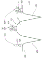
图1为侧视示意图,说明本发明铜箔基板的其中一实施方式。FIG. 1 is a schematic side view illustrating one embodiment of the copper foil substrate of the present invention.
图2为图1的II部分的放大示意图。FIG. 2 is an enlarged schematic view of part II of FIG. 1 .
图3为示意图,说明微粗糙电解铜箔的生产设备。Fig. 3 is a schematic diagram illustrating production equipment for micro-roughened electrolytic copper foil.
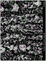
图4为扫描式电子显微镜图,说明实施例1微粗糙电解铜箔的表面形态。FIG. 4 is a scanning electron microscope image illustrating the surface morphology of the micro-roughened electrolytic copper foil of Example 1. FIG.
图5为扫描式电子显微镜图,说明实施例1微粗糙电解铜箔的截面形态。FIG. 5 is a scanning electron microscope image illustrating the cross-sectional shape of the micro-roughened electrolytic copper foil of Example 1. FIG.
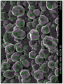
图6为扫描式电子显微镜图,说明比较例3的铜箔表面形态。FIG. 6 is a scanning electron microscope image illustrating the surface morphology of the copper foil of Comparative Example 3. FIG.
图7为扫描式电子显微镜图,说明比较例3的铜箔截面形态。FIG. 7 is a scanning electron micrograph illustrating the cross-sectional shape of the copper foil of Comparative Example 3. FIG.
具体实施方式Detailed ways
以下是通过特定的具体实施例来说明本发明所公开有关“微粗糙电解铜箔及铜箔基板”的实施方式,本领域技术人员可由本说明书所公开的内容了解本发明的优点与效果。本发明可通过其他不同的具体实施例加以施行或应用,本说明书中的各项细节也可基于不同观点与应用,在不悖离本发明的构思下进行各种修改与变更。另外,本发明的附图仅为简单示意说明,并非依实际尺寸的描绘,事先声明。以下的实施方式将进一步详细说明本发明的相关技术内容,但所公开的内容并非用以限制本发明的保护范围。The following are specific examples to illustrate the implementation of the "micro-roughened electrolytic copper foil and copper foil substrate" disclosed in the present invention. Those skilled in the art can understand the advantages and effects of the present invention from the content disclosed in this specification. The present invention can be implemented or applied through other different specific embodiments, and various modifications and changes can be made to the details in this specification based on different viewpoints and applications without departing from the concept of the present invention. In addition, the drawings of the present invention are only for simple illustration, and are not drawn according to the actual size, which is stated in advance. The following embodiments will further describe the relevant technical content of the present invention in detail, but the disclosed content is not intended to limit the protection scope of the present invention.
参阅图1,本发明铜箔基板1,包括一基材11以及二片微粗糙电解铜箔12。微粗糙电解铜箔12分别贴合在基材11的两相反侧。值得一提的是,铜箔基板1也可以仅包括一片微粗糙电解铜箔12。Referring to FIG. 1 , the copper foil substrate 1 of the present invention includes a substrate 11 and two pieces of micro-roughened
基材11较佳是具有低Dk值及低Df值,以抑制介入损失(insertion loss)。较佳地,所述基材11在10GHz频率下的Dk值小于或等于4且在10GHz频率下的Df值小于或等于0.020,更佳地,所述基材11在10GHz频率下的Dk值小于或等于3.8且在10GHz频率下的Df值小于或等于0.015。The substrate 11 preferably has a low Dk value and a low Df value to suppress insertion loss. Preferably, the Dk value of the substrate 11 at a frequency of 10 GHz is less than or equal to 4 and the Df value at a frequency of 10 GHz is less than or equal to 0.020, more preferably, the Dk value of the substrate 11 at a frequency of 10 GHz is less than or equal to Or equal to 3.8 and the Df value at 10GHz frequency is less than or equal to 0.015.
基材11可采用预浸片含浸合成树脂再固化而成的复合材料。预浸片可例举如:酚醛棉纸、棉纸、树脂制纤维布、树脂制纤维不织布、玻璃板、玻璃织布,或玻璃不织布。合成树脂可例举如:环氧树脂、聚酯树脂、聚酰亚胺树脂、氰酸酯树脂、双马来酰亚胺三嗪树脂、聚苯醚树脂,或酚树脂。合成树脂层可以是单层或多层,并没有一定的限制。基材11可选自但不限于EM891、IT958G、IT150DA、S7439G、MEGTRON 4、MEGTRON 6,或MEGTRON 7。The base material 11 can be a composite material obtained by impregnating a prepreg sheet with a synthetic resin and then curing it. The prepreg sheet may, for example, be phenolic tissue paper, tissue paper, resin fiber cloth, resin fiber nonwoven fabric, glass plate, glass woven fabric, or glass nonwoven fabric. The synthetic resin may, for example, be epoxy resin, polyester resin, polyimide resin, cyanate resin, bismaleimide triazine resin, polyphenylene ether resin, or phenol resin. The synthetic resin layer may be a single layer or a multilayer without limitation. The substrate 11 can be selected from but not limited to EM891, IT958G, IT150DA, S7439G, MEGTRON 4, MEGTRON 6, or MEGTRON 7.
参阅图1及图2,微粗糙电解铜箔12是对铜箔表面以电解法进行粗糙化处理而得。电解法粗糙化处理可对铜箔的任一表面进行处理,因此,微粗糙电解铜箔12具有位于至少一侧的微粗糙表面121。在本发明的其中一实施方式中,是取反转铜箔(Reverse Treatedcopper Foil,RTF)作为生箔,而后对其光泽面进一步执行粗糙化处理而获得微粗糙电解铜箔12。Referring to FIG. 1 and FIG. 2 , the micro-rough
微粗糙表面121用来贴附在基材11,其包括多个凸峰122、多个凹槽123以及多个微结晶簇124。两个相邻的凸峰122界定出一个凹槽123。凹槽123具有U形剖面轮廓及/或V形剖面轮廓,凹槽123的平均深度小于或等于1.5微米,较佳是小于或等于1.3微米,更佳是小于或等于1微米。凹槽123的平均宽度介于0.1至4微米。The
微结晶簇124的平均高度小于或等于2微米,较佳是小于或等于1.8微米,更佳是小于或等于1.6微米。前述的平均高度是指微结晶簇124顶部至凸峰122顶部的距离。微结晶簇124的平均最大宽度小于或等于5微米,较佳是小于或等于3微米。每一个微结晶簇124是由多个微结晶125堆栈构成,且微结晶125的平均直径小于或等于0.5微米,较佳是介于0.05至0.5微米,更佳是介于0.1至0.4微米。每一个微结晶簇124沿其自身高度方向的微结晶125平均堆栈数量是15个以下,较佳是13个以下,更佳是10个以下,又更佳是8个以下。微结晶125在堆栈成微结晶簇124时,可以迭成塔状结构,也可以向外延伸而呈现分岔结构,而构成分岔状的结晶团M。The average height of the
微结晶簇124彼此间的排列方式并没有一定,可以是无序的排列,也可以是大致沿着相同的方向排列,或者是以数个微结晶簇124排成一列且每列的延伸方向部分相同。The arrangement of the
微粗糙电解铜箔12的微粗糙表面121平均高度较佳是大于0.5微米,更佳是大于1.5微米,又更佳是大于2.0微米。当微粗糙表面121的平均粗糙度Rz符合前述范围时,就能与基材11间有良好的接合力表现,也就是说,当提高平均粗糙度Rz即可有效提高与基材11间的接合力,使得剥离强度(Peel strength)有效提高。较佳地,以1oz铜箔基板1来说,微粗糙电解铜箔12与基材11间的剥离强度大于4.3lb/in,较佳地是大于4.5lb/in,更佳地是大于4.7lb/in。因为在黏合于基板11时,涂覆在微粗糙表面上的黏胶会渗入到凹槽123及微结晶簇124的底部,所以黏合至基板11后能够有效提高剥离强度。The average height of the
透过前述微粗糙表面121的形态,微粗糙电解铜箔12与基材11间能具有足够的剥离强度,并且还能有效地抑制讯号传送时的损耗。微粗糙表面121的Rlr值低于1.3,较佳地是低于1.26,更佳地是低于1.23,又更佳地是低于1.2。所述的Rlr值是指展开长度比,也就是待测物在一单位长度之中的表面轮廓长度比。数值越高代表表面愈加崎岖,当数值等于1时,代表完全平整。Rlr满足关系式Rlr=Rlo/L。其中,Rlo是指被测的轮廓长度,L是指被测的距离。Through the shape of the aforementioned
当微粗糙电解铜箔12的Rlr值低于1.3时,铜箔基板1(如IT170GRA1+RG311)会有较佳的介入损失表现。铜箔基板1在8GHz时的介入损失介于0至-0.65db/in,更佳是介于0至-0.63db/in,又更佳是介于0至-0.60db/in,再更佳是介于0至-0.57db/in。铜箔基板1在12.89GHz的介入损失介于0至-1.0db/in,较佳是介于0至-0.97db/in,更佳地是介于0至-0.94db/in,又更佳地是介于0至-0.90db/in。铜箔基板1在16GHz的介入损失介于0至-1.2db/in,更佳地是介于0至-1.15db/in,又更佳地是介于0至-1.1db/in。铜箔基板1在20GHz的介入损失介于0至-1.5db/in,较佳地是介于0至-1.45db/in,更佳地是介于0至-1.4db/in,又更佳地是介于0至-1.36db/in,再更佳地是介于0至-1.34db/in。本发明的微粗糙电解铜箔12由频率4GHz至20GHz之间,皆能够有效地抑制讯号传送时的损耗。When the Rlr value of the micro-rough
[微粗糙电解铜箔制作方法][Manufacturing method of micro-rough electrolytic copper foil]
微粗糙电解铜箔12是将生箔浸入含铜镀液后,在一定的时间下进行电解粗糙化处理。本发明的实施方式中,是取反转铜箔(RTF)作为生箔,并对其粗糙面进行电解粗糙化处理。电解粗糙化处理可采用任何熟知的设备来进行,例如:连续式电解设备,或批次式电解设备。Micro-roughened
含铜镀液内含有铜离子、酸,以及金属添加剂。铜离子来源可例举如硫酸铜、硝酸铜,或其等的组合。酸可例举如硫酸、硝酸,或其等的组合。金属添加剂可例举如钴、铁、锌,或其等的组合。此外,含铜镀液还可以进一步添加熟知的添加剂,例如:明胶、有机氮化物、羟乙基纤维素(hydroxyethyl cellulose;HEC)、聚乙二醇(Poly(ethylene glycol)、PEG)、3-巯基-1-丙烷磺酸钠(Sodium 3-mercaptopropanesulphonate、MPS)、聚二硫二丙烷磺酸钠(Bis-(sodium sulfopropyl)-disulfide、SPS),或硫脲基化合物,但并不以此为限。Copper-containing baths contain copper ions, acids, and metal additives. The source of copper ions may, for example, be copper sulfate, copper nitrate, or a combination thereof. The acid may, for example, be sulfuric acid, nitric acid, or a combination thereof. Metal additives may, for example, be cobalt, iron, zinc, or a combination thereof. In addition, the copper-containing plating solution can further add well-known additives, such as: gelatin, organic nitrogen compounds, hydroxyethyl cellulose (hydroxyethyl cellulose; HEC), polyethylene glycol (Poly(ethylene glycol), PEG), 3- Sodium 3-mercaptopropanesulphonate (MPS), sodium polydisulfide dipropane sulfonate (Bis-(sodium sulfopropyl)-disulfide, SPS), or thiourea compounds, but not as such limit.
粗糙化处理的次数是至少二次,每一次粗糙化处理中的含铜镀液的组成可以相同或不同。在本发明的其中一实施方式中,是采用两组含铜镀液交替进行粗糙化处理,且第一组含铜镀液的铜离子浓度较佳是介于10至30g/l、酸浓度较佳是介于70至100g/l,且金属添加剂的添加量较佳是150至300mg/l。而第二组含铜镀液的铜离子浓度较佳是介于70至100g/l、酸浓度较佳是介于30至60g/l,且金属添加剂的添加量较佳是15至100mg/l。The number of roughening treatments is at least two times, and the composition of the copper-containing plating solution in each roughening treatment may be the same or different. In one embodiment of the present invention, two sets of copper-containing plating solutions are used to alternately carry out the roughening treatment, and the copper ion concentration of the first set of copper-containing plating solutions is preferably between 10 and 30 g/l, and the acid concentration is relatively low. Preferably it is between 70 and 100 g/l, and the metal additive is preferably added in an amount of 150 to 300 mg/l. The copper ion concentration of the second group of copper-containing plating solutions is preferably between 70 and 100 g/l, the acid concentration is preferably between 30 and 60 g/l, and the addition amount of metal additives is preferably between 15 and 100 mg/l .
电解的供电方法可采用定电压、定电流、脉冲型波形,或锯型波形,但不限于此。在本发明的其中一实施方式中,粗糙化处理是先采用第一组含铜镀液以定电流25至40A/dm2进行处理,而后再以第二组含铜镀液以定电流以定电流20至30A/dm2进行处理。较佳地,第一组含铜镀液以定电流30至56A/dm2进行处理,而第二组含铜镀液以定电流以定电流23至26A/dm2进行处理。需注意的是,前述定电流也能以脉冲型波形或锯型波形进行供电。此外,如要采用定电压进行供电,则须确保在各粗糙化处理的阶段中施加的电压值使电流值落于前述范围内。The power supply method of electrolysis can adopt constant voltage, constant current, pulse waveform, or saw waveform, but not limited thereto. In one embodiment of the present invention, the roughening treatment is firstly treated with the first group of copper-containing plating solutions at a constant current of 25 to 40A/dm 2 , and then the second group of copper-containing plating solutions is used at a constant current to constant Current 20 to 30A/dm 2 for treatment. Preferably, the first group of copper-containing plating solutions is treated with a constant current of 30 to 56 A/dm 2 , while the second group of copper-containing plating solutions is treated with a constant current of 23 to 26 A/dm 2 . It should be noted that the aforesaid constant current can also be supplied with pulse waveform or saw waveform. In addition, if a constant voltage is to be used for power supply, it must be ensured that the voltage value applied in each roughening treatment stage makes the current value fall within the aforementioned range.
当粗糙化处理的次数为三次以上时,能够采用前述第一组及第二组含铜镀液交替使用来进行粗糙化处理。电流值控制在介于1至60A/dm2。在本发明的其中一实施方式中,第三次及第四次粗糙化处理分别采用第一组含铜镀液及第二组含铜镀液,且电流值分别控制在1至8A/dm2及40至60A/dm2。第五次以后的粗糙化处理的电流值控制在小于或等于5A/dm2。需注意的是,前述定电流也能以脉冲型波形或锯型波形进行供电。此外,如果要采用定电压进行供电,则须确保在各粗糙化处理的阶段中施加的电压值让电流值落于前述范围内。When the number of roughening treatments is more than three times, the aforementioned first group and second group of copper-containing plating solutions can be used alternately for roughening treatment. The current value is controlled between 1 and 60A/dm 2 . In one embodiment of the present invention, the third and fourth roughening treatments use the first group of copper-containing plating solutions and the second group of copper-containing plating solutions respectively, and the current values are respectively controlled at 1 to 8A/dm 2 and 40 to 60A/dm 2 . The current value of the roughening treatment after the fifth time is controlled to be less than or equal to 5A/dm 2 . It should be noted that the aforesaid constant current can also be supplied with pulse waveform or saw waveform. In addition, if a constant voltage is to be used for power supply, it must be ensured that the voltage value applied in each roughening process makes the current value fall within the aforementioned range.
值得一提的是,微粗糙表面121的微结晶簇124排列方式及凹槽123延伸方向可透过含铜镀液的流场来进行控制。当不施加流场或形成紊流,即可使微结晶簇124间呈现无序排列;而当控制流场使其在铜箔表面沿着特定方向流动,就会形成有大致沿着相同的方向排列的结构。然而,控制微结晶簇124排列方式及凹槽123延伸方向的方式不以此为限制,也可以采用钢刷预先刻出刮痕来形成不定向的凹槽123,制造者能采用任何熟知的方式进行调整。It is worth mentioning that the arrangement of
本发明的其中一较佳实施方式中,采用多槽及多电解辊的连续式电解设备进行粗糙化处理。其中,各个槽内交替容装第一组含铜镀液及第二组含铜镀液。供电方法采用定电流。生产速度控制在5至20m/min。生产温度控制在20至60℃。In one of the preferred embodiments of the present invention, a continuous electrolytic device with multiple grooves and multiple electrolytic rollers is used for roughening treatment. Wherein, the first group of copper-containing plating solutions and the second group of copper-containing plating solutions are alternately accommodated in each tank. The power supply method adopts constant current. The production speed is controlled at 5 to 20m/min. The production temperature is controlled at 20 to 60°C.
需注意的是,前述微粗糙电解铜箔制作方法也可以用于处理高温延展铜箔(HighTemperature Elongation、HTE)或极低粗糙度铜箔(Very Low Profile、VLP)。It should be noted that the aforementioned micro-roughened electrolytic copper foil manufacturing method can also be used to process high temperature elongated copper foil (High Temperature Elongation, HTE) or very low roughness copper foil (Very Low Profile, VLP).
以上已将铜箔基板1的各层结构及制造方法进行说明,以下将以实施例1至3为例示,并与比较例1至4相比较,以说明本发明的优点。The layer structure and manufacturing method of the copper clad substrate 1 have been described above, and examples 1 to 3 will be taken as examples below, and compared with comparative examples 1 to 4 to illustrate the advantages of the present invention.
[实施例1][Example 1]
参阅图3,微粗糙电解铜箔是采用连续式电解设备2进行粗糙化处理。连续式电解设备2包括一个输料辊21、一个集料辊22、六个位在输料辊21与集料辊22间的槽23、六个分别放置在槽23上方的电解辊组24,以及六个分别位于槽23内的辅助辊组25。每一个槽23内设有一组白金电极231。每一个电解辊组24包括二个电解辊241。每一个辅助辊组25包括二个辅助辊251。每一个槽23内的白金电极231与对应的电解辊组24分别电性连接到外部电源供应器的阳极及阴极。Referring to FIG. 3 , the micro-rough electrolytic copper foil is roughened by continuous
在本实施例1中,采用反转铜箔(RTF)作为生箔,其购自金居开发有限公司(型号RG311)。生箔收卷于输料辊21,后依序绕行于电解辊组24及辅助辊组25,再卷收于集料辊22。各槽23内的含铜镀液组分及电镀条件如表1所示,其中,铜离子的来源是硫酸铜。极低粗糙度铜箔由第一槽至第六槽依序对生箔的粗糙面进行粗糙化处理,生产速度是10m/min,最后获得粗糙度Rz(JIS94)为小于或等于2.5um微米的微粗糙电解铜箔。而后,取二片微粗糙电解铜箔与一片基材IT170GRA1贴合,即完成制作。In this embodiment 1, reversed copper foil (RTF) was used as the raw foil, which was purchased from Jinju Development Co., Ltd. (model RG311). The raw foil is wound on the feeding
本实施例1以扫描式电子显微镜观测其表面及截面结构,分别显示于图4及图5。In Example 1, the surface and cross-sectional structure were observed with a scanning electron microscope, which are shown in FIG. 4 and FIG. 5 respectively.
本实施例1微粗糙电解铜箔的剥离强度,是先于微粗糙表面上涂覆铜硅烷偶合剂并黏合至基材IT170GRA1固化后,再依照IPC-TM-650 4.6.8测试方法来进行测量。测试结果列于表2。In Example 1, the peel strength of micro-rough electrolytic copper foil is firstly coated with copper silane coupling agent on the micro-rough surface and bonded to the substrate IT170GRA1 for curing, and then measured according to IPC-TM-650 4.6.8 test method . The test results are listed in Table 2.
本实施例1微粗糙电解铜箔的Rlr值,是采用形状量测雷射显微镜(厂商:Keyence,型号:VK-X100)进行量测。测试结果列于表2。The Rlr value of the microrough electrolytic copper foil in Example 1 is measured by a shape measuring laser microscope (manufacturer: Keyence, model: VK-X100). The test results are listed in Table 2.
本实施例1微粗糙电解铜箔的介入损失,使用Micro-strip line(特性阻抗50Ω)的方法进行测试,并分别于频率4GHz、8GHz、12.89GHz、16GHz,及20GHz进行检测。测试结果列于表2。In Example 1, the insertion loss of the micro-rough electrolytic copper foil was tested using the method of Micro-strip line (characteristic impedance 50Ω), and the detection was performed at frequencies of 4GHz, 8GHz, 12.89GHz, 16GHz, and 20GHz respectively. The test results are listed in Table 2.
[实施例2及3][Example 2 and 3]
生箔、电解设备及含铜镀液组分与实施例1相同,电镀条件如表1所示,生产速度是10m/min。而后,取二片微粗糙电解铜箔与一片基材IT170GRA1贴合,即完成制作。量测方式与实施例1相同,测试结果列于表2。Raw foil, electrolytic equipment and copper-containing plating solution components are the same as in Example 1, the electroplating conditions are as shown in Table 1, and the production speed is 10m/min. Then, take two pieces of micro-rough electrolytic copper foil and one piece of base material IT170GRA1 and stick them together to complete the production. The measurement method is the same as in Example 1, and the test results are listed in Table 2.
[比较例1及2][Comparative Examples 1 and 2]
生箔、电解设备及含铜镀液组分与实施例1相同,电镀条件如表1所示,生产速度是10m/min。而后,取二片微粗糙电解铜箔与一片基材IT170GRA1贴合,即完成制作。量测方式与实施例1相同,测试结果列于表2。Raw foil, electrolytic equipment and copper-containing plating solution components are the same as in Example 1, the electroplating conditions are as shown in Table 1, and the production speed is 10m/min. Then, take two pieces of micro-rough electrolytic copper foil and one piece of base material IT170GRA1 and stick them together to complete the production. The measurement method is the same as in Example 1, and the test results are listed in Table 2.
[比较例3][Comparative example 3]
采用三井金属所产的反转铜箔(型号:MLS-G,下称MLS-G铜箔),以扫描式电子显微镜图观测其表面及截面结构,分别显示于图6及图7。将二片MLS-G铜箔与一片基材IT170GRA1贴合后,量测其剥离强度、Rlr,以及介入损失,测试结果列于表2。The inverted copper foil produced by Mitsui Metals (model: MLS-G, hereinafter referred to as MLS-G copper foil) was used to observe its surface and cross-sectional structure with a scanning electron microscope, which are shown in Figure 6 and Figure 7 respectively. After laminating two pieces of MLS-G copper foil to one IT170GRA1 substrate, measure its peel strength, Rlr, and insertion loss. The test results are listed in Table 2.
[比较例4][Comparative example 4]
采用长春集团所产的反转铜箔(型号:RTF3,下称RTF3铜箔),以扫描式电子显微镜图观测其表面及截面结构。将二片RTF3铜箔与一片基材IT170GRA1贴合后,量测其剥离强度、Rlr,以及介入损失,测试结果列于表2。The reversed copper foil (model: RTF3, hereinafter referred to as RTF3 copper foil) produced by Changchun Group was used to observe its surface and cross-sectional structure with a scanning electron microscope. After laminating two pieces of RTF3 copper foil and one piece of substrate IT170GRA1, the peel strength, Rlr, and insertion loss were measured. The test results are listed in Table 2.
表1Table 1

表2Table 2

参阅图4及图5,实施例1的微粗糙表面具有多个沿着上下方向延伸的凹槽,且凹槽的延伸方向大致上平行。凹槽的宽度约介于0.1至4微米,深度小于或等于0.8微米。凹槽与凹槽间的凸峰处,有明显的微结晶簇形成于此。微结晶簇的高度小于或等于2微米,且每一个微结晶簇是由多数粒径介于0.1至0.4微米的微结晶堆栈而成。Referring to FIG. 4 and FIG. 5 , the micro-rough surface of embodiment 1 has a plurality of grooves extending along the vertical direction, and the extending directions of the grooves are substantially parallel. The width of the groove is about 0.1 to 4 microns, and the depth is less than or equal to 0.8 microns. At the peaks between the grooves, there are obvious microcrystalline clusters formed here. The height of the micro-crystal clusters is less than or equal to 2 microns, and each micro-crystal cluster is formed by stacking a plurality of micro-crystals with particle sizes ranging from 0.1 to 0.4 microns.
参阅图6及图7,MLS-G铜箔的表面是由多数粒径大于3微米的结晶均匀地披覆,且少数的微结晶相互聚集。由截面图得知,微结晶彼此间隔地分布在表面,并没有集中在特定的位置。Referring to Figure 6 and Figure 7, the surface of the MLS-G copper foil is evenly covered by crystals with a particle size greater than 3 microns, and a small number of microcrystals aggregate with each other. It can be seen from the cross-sectional view that the microcrystals are distributed on the surface at intervals, and are not concentrated in a specific position.
参阅表2,在剥离强度的表现上,实施例1至3的剥离强度至少为4.75lb/in,大于业界标准4lb/in至少18%。由此可见,本发明微粗糙电解铜箔与基材有良好的接合力,有利于后续制程的进行,并维持产品良率。Referring to Table 2, in terms of peel strength, the peel strength of Examples 1 to 3 is at least 4.75 lb/in, which is at least 18% greater than the industry standard of 4 lb/in. It can be seen that the micro-rough electrolytic copper foil of the present invention has a good bonding force with the substrate, which is beneficial to the subsequent process and maintains the product yield.
关于介入损失的表现,实施例1至3在频率8GHz至20GHz之间的介入损失,都优于比较例1至4。值得一提的是,通过控制微粗糙表面的表面形态以及将Rlr值调整至小于或等于1.3,明显可抑制铜箔基板在高频的讯号损失。此外,当Rlr值越低,可发现具有更进一步地降低讯号损失的效果。With regard to the performance of insertion loss, the insertion losses of Examples 1 to 3 at frequencies between 8 GHz and 20 GHz are better than those of Comparative Examples 1 to 4. It is worth mentioning that by controlling the surface morphology of the micro-rough surface and adjusting the Rlr value to be less than or equal to 1.3, the signal loss of the copper foil substrate at high frequencies can be significantly suppressed. In addition, the lower the Rlr value, the effect of further reducing the signal loss can be found.
由上述可知,本发明的微粗糙电解铜箔在维持良好的剥离强度下,进一步优化了介入损失的表现,能有效地抑制讯号损耗。From the above, it can be seen that the micro-roughened electrolytic copper foil of the present invention further optimizes the performance of insertion loss while maintaining good peel strength, and can effectively suppress signal loss.
以上所公开的内容仅为本发明的优选可行实施例,并非因此局限本发明的权利要求书的保护范围,所以凡是运用本发明说明书及附图内容所做的等效技术变化,均包含于本发明的权利要求书的保护范围内。The content disclosed above is only a preferred feasible embodiment of the present invention, and does not therefore limit the protection scope of the claims of the present invention. Therefore, all equivalent technical changes made by using the description of the present invention and the contents of the accompanying drawings are included in this document. within the protection scope of the claims of the invention.
Claims (6)
Priority Applications (1)
| Application Number | Priority Date | Filing Date | Title |
|---|---|---|---|
| CN201811173307.6A CN111031663B (en) | 2018-10-09 | 2018-10-09 | Copper foil substrate |
Applications Claiming Priority (1)
| Application Number | Priority Date | Filing Date | Title |
|---|---|---|---|
| CN201811173307.6A CN111031663B (en) | 2018-10-09 | 2018-10-09 | Copper foil substrate |
Publications (2)
| Publication Number | Publication Date |
|---|---|
| CN111031663A CN111031663A (en) | 2020-04-17 |
| CN111031663B true CN111031663B (en) | 2023-05-05 |
Family
ID=70190766
Family Applications (1)
| Application Number | Title | Priority Date | Filing Date |
|---|---|---|---|
| CN201811173307.6A Active CN111031663B (en) | 2018-10-09 | 2018-10-09 | Copper foil substrate |
Country Status (1)
| Country | Link |
|---|---|
| CN (1) | CN111031663B (en) |
Families Citing this family (1)
| Publication number | Priority date | Publication date | Assignee | Title |
|---|---|---|---|---|
| JP7270579B2 (en) | 2019-06-19 | 2023-05-10 | 金居開發股▲分▼有限公司 | Micro-roughened electrodeposited copper foil and copper-clad laminate |
Citations (5)
| Publication number | Priority date | Publication date | Assignee | Title |
|---|---|---|---|---|
| JP2004152904A (en) * | 2002-10-29 | 2004-05-27 | Kyocera Corp | Electrolytic copper foil, film with electrolytic copper foil, multilayer wiring board, and method of manufacturing the same |
| JP2008285751A (en) * | 2007-04-19 | 2008-11-27 | Mitsui Mining & Smelting Co Ltd | Surface treated copper foil, copper clad laminate obtained using the surface treated copper foil, and printed wiring board obtained using the copper clad laminate |
| JP2009218206A (en) * | 2008-02-15 | 2009-09-24 | Mitsui Mining & Smelting Co Ltd | Porous metal foil |
| CN105874891A (en) * | 2013-12-30 | 2016-08-17 | 日进材料股份有限公司 | Copper foil, and electrical component and battery including same |
| CN110952117A (en) * | 2018-09-27 | 2020-04-03 | 金居开发股份有限公司 | Micro-rough electrolytic copper foil and copper foil substrate |
-
2018
- 2018-10-09 CN CN201811173307.6A patent/CN111031663B/en active Active
Patent Citations (5)
| Publication number | Priority date | Publication date | Assignee | Title |
|---|---|---|---|---|
| JP2004152904A (en) * | 2002-10-29 | 2004-05-27 | Kyocera Corp | Electrolytic copper foil, film with electrolytic copper foil, multilayer wiring board, and method of manufacturing the same |
| JP2008285751A (en) * | 2007-04-19 | 2008-11-27 | Mitsui Mining & Smelting Co Ltd | Surface treated copper foil, copper clad laminate obtained using the surface treated copper foil, and printed wiring board obtained using the copper clad laminate |
| JP2009218206A (en) * | 2008-02-15 | 2009-09-24 | Mitsui Mining & Smelting Co Ltd | Porous metal foil |
| CN105874891A (en) * | 2013-12-30 | 2016-08-17 | 日进材料股份有限公司 | Copper foil, and electrical component and battery including same |
| CN110952117A (en) * | 2018-09-27 | 2020-04-03 | 金居开发股份有限公司 | Micro-rough electrolytic copper foil and copper foil substrate |
Also Published As
| Publication number | Publication date |
|---|---|
| CN111031663A (en) | 2020-04-17 |
Similar Documents
| Publication | Publication Date | Title |
|---|---|---|
| JP7317924B2 (en) | Micro-roughened electrodeposited copper foil and copper-clad laminate | |
| WO2016088884A1 (en) | Surface-treated copper foil for forming high frequency signal transmission circuit, copper clad laminate board and printed wiring board | |
| KR102655111B1 (en) | Electrodeposited copper foil with its surfaceprepared, process for producing the same and usethereof | |
| TWI669032B (en) | Micro-rough electrolytic copper foil and copper foil substrate | |
| TWI719698B (en) | Advanced reverse treated electrodeposited copper foil and copper clad laminate using the same | |
| CN111031663B (en) | Copper foil substrate | |
| TWI668333B (en) | Micro-rough electrolytic copper foil and copper foil substrate | |
| TWI736325B (en) | Advanced reverse-treated electrodeposited copper foil having long and island-shaped structures and copper clad laminate using the same | |
| TWI695898B (en) | Micro-roughened electrolytic copper foil and copper clad laminate using the same | |
| CN110952117B (en) | Micro-rough electrolytic copper foil and copper foil substrate | |
| CN117364182A (en) | Ultralow-profile RTF copper foil, preparation method and electrolyte for ultralow-profile RTF copper foil nodulation treatment | |
| CN111194134B (en) | Micro-roughened electrolytic copper foil and copper-clad substrate using the same | |
| JP2021008665A (en) | Advanced electrolytic copper foil and copper-clad laminate to which it is applied | |
| JP2021021137A (en) | Advanced treated electrodeposited copper foil having long and island-shaped structures and copper clad laminate using the same | |
| CN121218458A (en) | An electrolytic copper foil, its preparation method and its application | |
| CN119372726A (en) | A roughening liquid for roughening the surface of reverse copper foil and a method for preparing reverse copper foil | |
| CN118653185A (en) | Electrolyte, electrolytic copper foil and preparation method thereof |
Legal Events
| Date | Code | Title | Description |
|---|---|---|---|
| PB01 | Publication | ||
| PB01 | Publication | ||
| SE01 | Entry into force of request for substantive examination | ||
| SE01 | Entry into force of request for substantive examination | ||
| GR01 | Patent grant | ||
| GR01 | Patent grant |