CN110943778B - Optical communication device and method for transmitting and receiving information - Google Patents
Optical communication device and method for transmitting and receiving information Download PDFInfo
- Publication number
- CN110943778B CN110943778B CN201811119052.5A CN201811119052A CN110943778B CN 110943778 B CN110943778 B CN 110943778B CN 201811119052 A CN201811119052 A CN 201811119052A CN 110943778 B CN110943778 B CN 110943778B
- Authority
- CN
- China
- Prior art keywords
- light source
- information
- image
- optical communication
- driving
- Prior art date
- Legal status (The legal status is an assumption and is not a legal conclusion. Google has not performed a legal analysis and makes no representation as to the accuracy of the status listed.)
- Active
Links
Images


Classifications
-
- G—PHYSICS
- G06—COMPUTING; CALCULATING OR COUNTING
- G06K—GRAPHICAL DATA READING; PRESENTATION OF DATA; RECORD CARRIERS; HANDLING RECORD CARRIERS
- G06K7/00—Methods or arrangements for sensing record carriers, e.g. for reading patterns
- G06K7/10—Methods or arrangements for sensing record carriers, e.g. for reading patterns by electromagnetic radiation, e.g. optical sensing; by corpuscular radiation
-
- H—ELECTRICITY
- H04—ELECTRIC COMMUNICATION TECHNIQUE
- H04B—TRANSMISSION
- H04B10/00—Transmission systems employing electromagnetic waves other than radio-waves, e.g. infrared, visible or ultraviolet light, or employing corpuscular radiation, e.g. quantum communication
- H04B10/11—Arrangements specific to free-space transmission, i.e. transmission through air or vacuum
-
- G—PHYSICS
- G06—COMPUTING; CALCULATING OR COUNTING
- G06K—GRAPHICAL DATA READING; PRESENTATION OF DATA; RECORD CARRIERS; HANDLING RECORD CARRIERS
- G06K7/00—Methods or arrangements for sensing record carriers, e.g. for reading patterns
- G06K7/10—Methods or arrangements for sensing record carriers, e.g. for reading patterns by electromagnetic radiation, e.g. optical sensing; by corpuscular radiation
- G06K7/14—Methods or arrangements for sensing record carriers, e.g. for reading patterns by electromagnetic radiation, e.g. optical sensing; by corpuscular radiation using light without selection of wavelength, e.g. sensing reflected white light
- G06K7/1404—Methods for optical code recognition
- G06K7/146—Methods for optical code recognition the method including quality enhancement steps
-
- G—PHYSICS
- G06—COMPUTING; CALCULATING OR COUNTING
- G06K—GRAPHICAL DATA READING; PRESENTATION OF DATA; RECORD CARRIERS; HANDLING RECORD CARRIERS
- G06K19/00—Record carriers for use with machines and with at least a part designed to carry digital markings
- G06K19/06—Record carriers for use with machines and with at least a part designed to carry digital markings characterised by the kind of the digital marking, e.g. shape, nature, code
- G06K19/06009—Record carriers for use with machines and with at least a part designed to carry digital markings characterised by the kind of the digital marking, e.g. shape, nature, code with optically detectable marking
- G06K19/06018—Record carriers for use with machines and with at least a part designed to carry digital markings characterised by the kind of the digital marking, e.g. shape, nature, code with optically detectable marking one-dimensional coding
- G06K19/06028—Record carriers for use with machines and with at least a part designed to carry digital markings characterised by the kind of the digital marking, e.g. shape, nature, code with optically detectable marking one-dimensional coding using bar codes
-
- G—PHYSICS
- G06—COMPUTING; CALCULATING OR COUNTING
- G06K—GRAPHICAL DATA READING; PRESENTATION OF DATA; RECORD CARRIERS; HANDLING RECORD CARRIERS
- G06K7/00—Methods or arrangements for sensing record carriers, e.g. for reading patterns
- G06K7/10—Methods or arrangements for sensing record carriers, e.g. for reading patterns by electromagnetic radiation, e.g. optical sensing; by corpuscular radiation
- G06K7/10544—Methods or arrangements for sensing record carriers, e.g. for reading patterns by electromagnetic radiation, e.g. optical sensing; by corpuscular radiation by scanning of the records by radiation in the optical part of the electromagnetic spectrum
- G06K7/10712—Fixed beam scanning
- G06K7/10722—Photodetector array or CCD scanning
- G06K7/10732—Light sources
-
- G—PHYSICS
- G06—COMPUTING; CALCULATING OR COUNTING
- G06K—GRAPHICAL DATA READING; PRESENTATION OF DATA; RECORD CARRIERS; HANDLING RECORD CARRIERS
- G06K7/00—Methods or arrangements for sensing record carriers, e.g. for reading patterns
- G06K7/10—Methods or arrangements for sensing record carriers, e.g. for reading patterns by electromagnetic radiation, e.g. optical sensing; by corpuscular radiation
- G06K7/10544—Methods or arrangements for sensing record carriers, e.g. for reading patterns by electromagnetic radiation, e.g. optical sensing; by corpuscular radiation by scanning of the records by radiation in the optical part of the electromagnetic spectrum
- G06K7/10712—Fixed beam scanning
- G06K7/10722—Photodetector array or CCD scanning
- G06K7/10752—Exposure time control
-
- G—PHYSICS
- G06—COMPUTING; CALCULATING OR COUNTING
- G06K—GRAPHICAL DATA READING; PRESENTATION OF DATA; RECORD CARRIERS; HANDLING RECORD CARRIERS
- G06K7/00—Methods or arrangements for sensing record carriers, e.g. for reading patterns
- G06K7/10—Methods or arrangements for sensing record carriers, e.g. for reading patterns by electromagnetic radiation, e.g. optical sensing; by corpuscular radiation
- G06K7/14—Methods or arrangements for sensing record carriers, e.g. for reading patterns by electromagnetic radiation, e.g. optical sensing; by corpuscular radiation using light without selection of wavelength, e.g. sensing reflected white light
- G06K7/1404—Methods for optical code recognition
-
- H—ELECTRICITY
- H04—ELECTRIC COMMUNICATION TECHNIQUE
- H04B—TRANSMISSION
- H04B10/00—Transmission systems employing electromagnetic waves other than radio-waves, e.g. infrared, visible or ultraviolet light, or employing corpuscular radiation, e.g. quantum communication
- H04B10/11—Arrangements specific to free-space transmission, i.e. transmission through air or vacuum
- H04B10/114—Indoor or close-range type systems
- H04B10/116—Visible light communication
-
- H—ELECTRICITY
- H04—ELECTRIC COMMUNICATION TECHNIQUE
- H04B—TRANSMISSION
- H04B10/00—Transmission systems employing electromagnetic waves other than radio-waves, e.g. infrared, visible or ultraviolet light, or employing corpuscular radiation, e.g. quantum communication
- H04B10/40—Transceivers
-
- H—ELECTRICITY
- H04—ELECTRIC COMMUNICATION TECHNIQUE
- H04B—TRANSMISSION
- H04B10/00—Transmission systems employing electromagnetic waves other than radio-waves, e.g. infrared, visible or ultraviolet light, or employing corpuscular radiation, e.g. quantum communication
- H04B10/50—Transmitters
- H04B10/572—Wavelength control
-
- H—ELECTRICITY
- H04—ELECTRIC COMMUNICATION TECHNIQUE
- H04N—PICTORIAL COMMUNICATION, e.g. TELEVISION
- H04N23/00—Cameras or camera modules comprising electronic image sensors; Control thereof
- H04N23/50—Constructional details
- H04N23/54—Mounting of pick-up tubes, electronic image sensors, deviation or focusing coils
-
- H—ELECTRICITY
- H04—ELECTRIC COMMUNICATION TECHNIQUE
- H04N—PICTORIAL COMMUNICATION, e.g. TELEVISION
- H04N23/00—Cameras or camera modules comprising electronic image sensors; Control thereof
- H04N23/56—Cameras or camera modules comprising electronic image sensors; Control thereof provided with illuminating means
-
- G—PHYSICS
- G06—COMPUTING; CALCULATING OR COUNTING
- G06K—GRAPHICAL DATA READING; PRESENTATION OF DATA; RECORD CARRIERS; HANDLING RECORD CARRIERS
- G06K7/00—Methods or arrangements for sensing record carriers, e.g. for reading patterns
- G06K7/10—Methods or arrangements for sensing record carriers, e.g. for reading patterns by electromagnetic radiation, e.g. optical sensing; by corpuscular radiation
- G06K2007/10485—Arrangement of optical elements
Abstract
Optical communication devices and methods for transmitting and receiving information are disclosed. The optical communication device includes: at least two light sources including a first light source and a second light source; and a controller capable of driving the first and second light sources through at least two driving modes including a first driving mode and a second driving mode, the first and second driving modes having the same or different frequencies, wherein when the first and second light sources are driven in the same driving mode, first information is transmitted; when the first light source and the second light source are driven in different driving modes, for transmitting other information different from the first information.
Description
Technical Field
The present invention is in the field of optical information technology, and more particularly relates to an optical communication device (also referred to herein as an "optical tag") and a method for transmitting and receiving information.
Background
Bar codes and two-dimensional codes have been widely used to encode information. When these bar codes and two-dimensional codes are scanned with a specific device or software, the corresponding information is recognized. However, the identification distance of the barcode and the two-dimensional code is very limited. For example, for a two-dimensional code, when scanned by a camera of a mobile phone, the mobile phone must be placed within a relatively close distance, which is typically only about 15 times the width of the two-dimensional code. Therefore, the normal size bar code and the two-dimensional code cannot be recognized at a long distance. Remote identification can be achieved by customizing very large bar codes and two-dimensional codes, but this brings a significant rise in cost and is impossible to achieve in many cases due to other various limitations (e.g., space limitations).
Bar codes and two-dimensional codes are inconvenient in many application scenarios due to their limitations in terms of identification distance. For example, when a user purchases a ticket or purchases a commodity by scanning a posted two-dimensional code through a mobile phone, if the number of people is too large, people far away from the two-dimensional code cannot recognize the two-dimensional code through the mobile phone, and the user needs to wait for the previous people to leave and then approach the two-dimensional code to perform corresponding operations, which is time-consuming and inconvenient. Therefore, there is a need in the art for a solution that enables remote information identification.
Disclosure of Invention
One aspect of the present invention relates to an optical communication apparatus including: at least two light sources including a first light source and a second light source; and a controller capable of driving the first and second light sources through at least two driving modes including a first driving mode and a second driving mode, the first and second driving modes having the same or different frequencies, wherein when the first and second light sources are driven in the same driving mode, first information is transmitted; when the first light source and the second light source are driven in different driving modes, for transmitting other information different from the first information.
Another aspect of the present invention relates to a method of transmitting information using at least two light sources, wherein the at least two light sources include a first light source and a second light source, the first and second light sources being drivable by at least two driving modes, the at least two driving modes including a first driving mode and a second driving mode, the first driving mode and the second driving mode having the same or different frequencies, the method comprising: when first information needs to be transmitted, driving the first light source and the second light source in the same driving mode; and driving the first light source and the second light source in different driving modes when other information different from the first information needs to be transmitted.
Another aspect of the invention relates to an apparatus for transmitting information using at least two light sources, comprising a controller for controlling the at least two light sources, the controller being configured to implement the above method.
Another aspect of the invention relates to an optical communication system comprising: the optical communication device described above; and means for identifying information transmitted by the optical communication device configured to: imaging the optical communication device; extracting an image of a first light source in the optical communication device and an image of a second light source in the optical communication device; comparing the image of the first light source and the image of the second light source; and determining information jointly conveyed by the first light source and the second light source based at least in part on a result of the comparison.
Another aspect of the invention relates to a method for receiving information transmitted by an optical communication device, the method comprising: imaging the optical communication device; extracting an image of a first light source in the optical communication device and an image of a second light source in the optical communication device; comparing the image of the first light source and the image of the second light source; and determining information jointly conveyed by the first light source and the second light source based at least in part on a result of the comparison.
Another aspect of the invention relates to an apparatus for receiving information transmitted by an optical communication apparatus, comprising an imaging device, a processor and a memory, the memory having stored therein a computer program which, when executed by the processor, is operable to carry out the above-mentioned method.
Another aspect of the invention relates to a storage medium in which a computer program is stored which, when being executed, can be used for carrying out the above-mentioned method.
The invention obtains the information transmitted by a pair of light sources by comparing the images of the light sources which are mutually referenced and matched with each other (rather than analyzing the image of a certain light source independently), avoids the influence of environmental illumination conditions, interference, noise and the like, can improve the accuracy and stability of the identification of the information transmitted by the light sources, and is particularly suitable for remote identification and outdoor identification. Furthermore, it is further advantageous that since the invention obtains the information conveyed by the light sources by comparing the images of a pair of light sources, it is not necessary to include a large number of fringes (or even a complete fringe in some cases) in the image of each light source, which further facilitates remote identification and allows a reduction in the signal frequency of the driving pattern used to generate the fringes in the image of the light source.
Drawings
Embodiments of the invention are further described below with reference to the accompanying drawings, in which:
FIG. 1 is a schematic diagram of a CMOS imager device;
FIG. 2 is a directional diagram of an image acquired by a CMOS imager;
FIG. 3 is a light source according to one embodiment of the present invention;
FIG. 4 is a light source according to another embodiment of the present invention;
FIG. 5 is an imaging timing diagram for a CMOS imager;
FIG. 6 is another imaging timing diagram for a CMOS imager;
fig. 7 shows an imaging diagram on a CMOS imager at different stages when the light source is driven in a certain drive mode;
FIG. 8 illustrates an imaging timing diagram for a CMOS imager according to an embodiment of the invention;
fig. 9 shows an imaging timing diagram of a CMOS imager device in accordance with an embodiment of the invention;
fig. 10 shows an imaging timing diagram of a CMOS imager device in accordance with an embodiment of the invention;
FIG. 11 shows an imaging timing diagram for a CMOS imager for implementing different stripes than FIG. 10, in accordance with one embodiment of the invention;
FIG. 12 illustrates an optical label according to one embodiment of the present invention;
FIG. 13 illustrates an optical label according to another embodiment of the invention;
fig. 14 shows an imaging timing diagram of a CMOS imager device according to an embodiment of the invention;
FIG. 15 shows a real imaging diagram implemented by controlling three light sources in a similar manner to FIG. 14;
FIG. 16 shows a physical image of an optical label using different stripe widths to effect information transfer;
FIG. 17 is a schematic view of an optical label including a location indicator according to one embodiment of the present invention; and
FIG. 18 illustrates an optical label including a locating mark according to one embodiment of the present invention when viewed with the naked eye.
Detailed Description
In order to make the objects, technical solutions and advantages of the present invention more apparent, the present invention will be further described in detail by way of specific embodiments with reference to the accompanying drawings.
One embodiment of the present invention relates to an optical communication device, also referred to herein as an "optical label," which may be used interchangeably throughout this application.
The optical communication device includes a light source, and light emitted by the light source can be sensed by the optical imaging device, and the light can be light which can be sensed by human eyes or light which can not be sensed by the human eyes. The light emitted by the light source may have a particular intensity, color, wavelength, etc. When the light source is operated, the light source may be imaged using an imaging device or a device having an imaging device (e.g., a cell phone, a tablet, smart glasses, etc.). The light source may be various types of light sources, for example, it may be one LED lamp, an array of a plurality of LED lamps, a display screen, or a part thereof, and even an irradiation area of light (for example, an irradiation area of light on a wall) may be used as the light source. The shape of the light source may be various shapes such as a circle, a square, a rectangle, a bar, an L-shape, etc. Various common optical devices may be included in the light source, such as light guide plates, diffuser plates, diffusers, and the like. In a preferred embodiment, the light source may be a two-dimensional array of a plurality of LED lights, one dimension of which is longer than the other, preferably in a ratio of about 5-12: 1. for example, the LED lamp array may be constituted by a plurality of LED lamps arranged in a line. The LED light array may appear as a generally elongated light source when illuminated, and the operation of the light source is controlled by the controller.
In another embodiment, the light source may not be limited to a planar light source, but may be implemented as a solid light source, for example, a bar-shaped cylindrical light source, a cubic light source, a spherical light source, or the like. The light source may be placed on a square, suspended at a location in an indoor location (e.g., a restaurant, a conference room, etc.), for example, so that nearby users in all directions may photograph the light source via a cell phone to obtain information conveyed by the light source.
CMOS imaging devices, which are currently widely used in electronic devices, generally use a rolling shutter imaging mode, i.e., individual pixels in a frame of an image are not exposed simultaneously (e.g., pixels are exposed in a line-by-line manner). The present invention advantageously utilizes this non-simultaneous exposure characteristic of the rolling shutter imaging manner, so that when a light source is driven by different driving modes, various different stripe patterns or no stripe patterns can be presented on an image of the light source obtained when the light source is photographed by a rolling shutter imaging device. By analyzing and identifying the pattern in the light source image, the identification of the information transmitted by the optical communication device can be realized.
Fig. 1 shows an example CMOS imaging device that includes an array of image sensors (also referred to as image sensing cells) and some other elements. Each image sensor in the array of image sensors corresponds to a pixel. Each column of image sensors is connected to a column amplifier, the output signal of which is then sent to an a/D converter (ADC) for analog-to-digital conversion and then output via an interface circuit. For any image sensor in the image sensor array, the exposure is cleared when the exposure is started, and then the signal value is read after the exposure time is over. CMOS imaging devices typically employ a rolling shutter imaging approach. In the CMOS imaging device, the readout of data is serial, so the clear/expose/readout is also performed sequentially line by line only in a pipeline-like manner, and combined into one frame image after all the lines of the image sensor array have been processed. Thus, the entire CMOS image sensor array is actually exposed row by row (in some cases the CMOS image sensor array may also be exposed row by row at a time), which results in a small time delay between the rows. Due to this small time delay, when the light source flashes at a certain frequency (e.g., by turning the light source on and off), stripes appear on the image taken by the CMOS imaging device.
When the light source is operated, the light source may be imaged using a CMOS imaging device or a device having a CMOS imaging device (e.g., a mobile phone, a tablet computer, smart glasses, etc.), that is, by means of a rolling shutter. Hereinafter, a mobile phone will be described as an example of a CMOS imager, as shown in fig. 2. The line scan direction of the handset is shown as vertical in fig. 2, but those skilled in the art will appreciate that the line scan direction may also be horizontal depending on the underlying hardware configuration.
Fig. 3 shows a light source according to an embodiment of the invention. When the light source shown in fig. 3 is imaged using the CMOS imaging device, it is preferable to make the long side of the light source shown in fig. 3 perpendicular or substantially perpendicular to the row direction of the CMOS imaging device (for example, the row scanning direction of the mobile phone shown in fig. 2) so as to image as many stripes as possible under the same other conditions. However, sometimes a user does not know the line scanning direction of his mobile phone, and in order to ensure that the mobile phone can recognize in various postures and can reach the maximum recognition distance in both the portrait screen and the landscape screen, the light source may be a combination of a plurality of rectangles, for example, an L-shaped light source as shown in fig. 4.
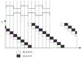
Fig. 5 shows an imaging timing diagram for a CMOS imager device, where each row corresponds to a row of sensors for the CMOS imager device. In imaging each row of a CMOS imaging sensor array, two phases are mainly involved, exposure time and readout time, respectively. There is a possibility that the exposure times of the rows overlap, but the readout times do not overlap.
It should be noted that only a small number of rows are schematically shown in fig. 5, which depends on the actual CMOS imaging deviceThe difference in resolution is typically thousands of rows of sensors. For example, for a 1080p resolution, it has 1920 × 1080 pixels, numeral 1080 indicates 1080 scan lines, and numeral 1920 indicates 1920 pixels per line. For 1080p resolution, the readout time per row is approximately 8.7 microseconds (i.e., 8.7 × 10)-6Seconds).
If the exposure time is too long, resulting in a large amount of overlap between the exposure times of adjacent rows, then a stripe may appear as a distinct transition in the imaging, e.g., a plurality of rows of pixels having different gray levels between a row of purely black pixels and a row of purely white pixels. The present invention contemplates that the pixel rows be rendered as sharp as possible, for which the exposure time for each row of a CMOS imager (e.g., a cell phone) may be set or adjusted (e.g., by an APP installed on the cell phone) to select a relatively short exposure time. In a preferred embodiment, the exposure time may be made approximately equal to or less than the readout time for each row. Taking 1080p resolution as an example, the readout time per line is approximately 8.7 microseconds, in which case it is contemplated to adjust the exposure time of the handset to approximately 8.7 microseconds or less. Fig. 6 shows an imaging timing chart of the CMOS imaging device in this case. In this case, the exposure times of the lines do not substantially overlap, or overlap is less, so that a streak having a clearer boundary can be obtained at the time of imaging, which is more easily recognized. It should be noted that fig. 6 is only a preferred embodiment of the present invention, and that longer (e.g., equal to or less than twice, three times, or four times the readout time per row, etc.) or shorter exposure times are also possible. For example, the readout time per line may be approximately 8.7 microseconds, while the set exposure time per line is 14 microseconds. In addition, in order to exhibit the streak, it is preferable that the duration of one period of the signal of the driving pattern of the light source be set to about twice the exposure duration or longer.
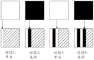
Fig. 7 shows the imaging diagram on the CMOS imager at different stages when the controller turns the light source on and off at a certain frequency in a certain driving mode. Specifically, the upper part of fig. 7 shows a state change diagram of the light source at different stages (white corresponds to the light source being turned on, and black corresponds to the light source being turned off), and the lower part shows an imaging diagram of the light source on the CMOS imaging device at different stages, wherein the row direction of the CMOS imaging device is the vertical direction and scans from left to right. Since the image collected by the CMOS imaging device is scanned line by line, when a high-frequency flicker signal is captured, a portion of the obtained one-frame image corresponding to the imaging position of the light source may form a stripe as shown in the lower part of fig. 7, specifically, in a period 1, the light source is turned on, and the scanning line of the leftmost part exposed in the period shows a bright stripe; in a period 2, the light source is turned off, and the scanning line exposed in the period presents dark stripes; in a period 3, the light source is turned on, and the scanning line exposed in the period shows bright stripes; in period 4, the light source is turned off, and the scan line exposed in this period appears dark striped.
The controller may adjust the width of the stripes that appear by setting the frequency at which the light source flashes via the drive pattern, or by setting the duration of each turn on and off of the light source. Longer on or off times generally correspond to wider stripes. For example, in the case shown in fig. 6, if the time length of each turn-on and turn-off of the light source is set to be approximately equal to the exposure time of each line of the CMOS imaging device (the exposure time may be set by the APP mounted on the mobile phone or manually set), it is possible to present a stripe having a width of only one pixel at the time of imaging. If the time period of each turn-on or turn-off of the light source is set to be approximately equal to approximately 2 times the exposure time period of each line of the CMOS imaging device, a stripe having a width of approximately two pixels can be realized, as shown in fig. 8 in particular, where the upper part of fig. 8 shows a signal waveform of a driving mode of the light source, a high level of which may correspond to the turn-on of the light source, and a low level of which may correspond to the turn-off of the light source. The signal frequency of the drive mode of fig. 8 may be, for example, 16000 times per second (each cycle having a duration of 62.5 microseconds, with an on-duration and an off-duration each of about 31.25 microseconds). In the embodiment shown in fig. 8, the duty ratio of the signal of the driving pattern is set to about 50%, and the exposure time period of each line is set to be approximately equal to the readout time of each line, but those skilled in the art will appreciate that other settings are possible as long as distinguishable stripes can be exhibited. For simplicity of description, fig. 8 uses synchronization between the light source and the CMOS imager such that the on and off times of the light source approximately correspond to the start or end times of the exposure duration of a row of the CMOS imager, but those skilled in the art will appreciate that even if the two are not synchronized as in fig. 8, a significant stripe may appear on the CMOS imager, where there may be some transition stripes, but there must be a row exposed when the light source is always off (i.e., the darkest stripe) and a row exposed when the light source is always on (i.e., the brightest stripe), separated by one pixel. Such a change in brightness (i.e., a streak) of a line of pixels can be readily detected (e.g., by comparing the brightness or gray scale of some pixels in the imaging area of the light source). Further, even if there is no line exposed when the light source is always off (i.e., the darkest stripe) and no line exposed when the light source is always on (i.e., the brightest stripe), if there are a line in which the light source-on portion t1 is less than a certain length of time or occupies a small proportion of the entire exposure time (i.e., the darker stripe) and a line in which the light source-on portion t2 is greater than a certain length of time or occupies a large proportion of the entire exposure time (i.e., the lighter stripe) during the exposure time, and t2-t1> the light-dark stripe difference threshold (e.g., 10 microseconds), or t2/t1> the light-dark stripe proportion threshold (e.g., 2), a change in brightness between these pixel lines can be detected. The light and shade stripe difference value threshold and the proportion threshold are related to the light intensity of the cursor label, the property of the photosensitive device, the shooting distance and the like. It will be appreciated by those skilled in the art that other thresholds are possible, as long as a computer-resolvable fringe pattern is exhibited.
The stripe pattern recognition method according to an embodiment of the present invention is as follows: obtaining an image of the optical label, and segmenting an imaging area of the light source by using a projection mode; collecting striped and non-striped pictures in different configurations (e.g., different distances, different light source blinking frequencies, etc.); all collected pictures are normalized uniformly to a specific size, for example 64 x 16 pixels; extracting each pixel feature (such as brightness, color and the like) as an input feature, and constructing a machine learning classifier; and performing classification judgment to judge whether the image is a stripe image or a non-stripe image. For the stripe recognition, any other method known in the art can be used for processing by those skilled in the art, and will not be described in detail.
For a strip light source with a length of 5 cm, when a camera is shot at a distance of 10 m (i.e. at a distance of 200 times the length of the light source) with a resolution of 1080p using a conventional mobile phone on the market, the strip light source occupies 6 pixels in the length direction, and if each stripe has a width of 2 pixels, at least one distinct stripe appears in the width range of 6 pixels, which can be easily recognized. If a higher resolution is set, or optical zoom is used, the fringes can also be identified at a greater distance, for example a distance of 300 or 400 times the length of the light source.
The controller may also drive the light source by different driving modes, for example to switch the light source on and off at another frequency. For the case shown in fig. 6, the light source may be configured to turn on and off at least once, for example 64000 times per second or more, during the exposure time of each row of the CMOS imaging device. Fig. 9 shows a case where the light source is turned on and off only once in the exposure time of each line, wherein the upper part of fig. 9 shows a signal waveform of a driving pattern of the light source, and a high level thereof may correspond to the turning on of the light source and a low level thereof may correspond to the turning off of the light source. Since the light source is turned on and off once in the same manner during the exposure time of each row, the exposure intensity energy obtained during each exposure time is approximately equal, and therefore, the brightness of each pixel row of the final image of the light source does not have obvious difference, and stripes do not exist. It will be appreciated by those skilled in the art that higher on and off frequencies are also possible. In addition, for simplicity of description, synchronization between the light source and the CMOS imaging device is used in fig. 9 so that the turn-on time of the light source approximately corresponds to the start time of the exposure time period of a certain line of the CMOS imaging device, but those skilled in the art will appreciate that even if the two are not synchronized as in fig. 9, there is no significant difference in brightness between the respective pixel lines of the final imaging of the light source, and thus no streak exists.
In another embodiment, when the presence of the streak is not desired, direct current may be supplied to the light source so that the light source emits light with a substantially constant intensity, whereby the streak is not present on one frame image of the light source obtained when the light source is photographed by the CMOS image sensor. In this case, it is also possible to achieve approximately the same luminous flux in the different drive modes to avoid flickering phenomena that may be perceived by the human eye when switching between the different drive modes. In addition, it can be understood that when the light source of the present invention is continuously operated in a certain driving mode, human eyes will not perceive any flickering phenomenon.
While fig. 8 above describes an embodiment in which the stripes are presented by varying the intensity of light emitted by the light source (e.g., by turning the light source on or off), in another embodiment, the stripes may also be presented by causing the light source to emit light of a different wavelength or color, as shown in fig. 10. In the embodiment shown in fig. 10, the light source includes a red light emitting red light and a blue light emitting blue light. The upper part of fig. 10 shows signals of a light source driving mode, which includes a red light driving signal and a blue light driving signal, wherein a high level corresponds to the turn-on of the corresponding light source, and a low level corresponds to the turn-off of the corresponding light source. The red and blue drive signals are phase shifted by 180, i.e. the levels are opposite. The light source can be made to alternately emit red light and blue light outward by the red light driving signal and the blue light driving signal, so that red and blue stripes can be presented when the light source is imaged by the CMOS imaging device.
In one embodiment, stripes of different widths may be implemented based on different signal frequencies of the light source drive mode, e.g., in a first drive mode, the light source may operate as shown in fig. 8, thereby implementing a first type of stripe having a width of about two pixels; in the second driving mode, the duration of the high level and the low level in each period of the signal of the light source driving mode in fig. 8 may be modified to be twice, respectively, for example, the LED lamp blinking frequency may be set 8000 times per second (the duration of each period is 125 microseconds, where the on-time and the off-time are each about 62.5 microseconds), thereby implementing the second stripe having a width of about four pixels, as shown in fig. 11 in particular.
In another embodiment, stripes with different colors may be implemented, for example, the light source may be set to include a red light capable of emitting red light and a blue light capable of emitting blue light, and in the first driving mode, the blue light may be turned off, and the red light may operate as shown in fig. 8, thereby implementing red-black stripes; in the second driving mode, the red lamp may be turned off and the blue lamp may be operated as shown in fig. 8, thereby implementing the blue-black stripe. In the above-described embodiment, the red-black stripe and the blue-black stripe are implemented using the same signal frequency in the first driving mode and the second driving mode, but it is understood that different signal frequencies may be used in the first driving mode and the second driving mode.
In addition, it will be understood by those skilled in the art that more than two stripes may be further implemented, for example, in the embodiment including the red lamp and the blue lamp in the light source described above, a third driving mode may be further provided in which the red lamp and the blue lamp are controlled in the manner shown in fig. 10 to implement the red-blue stripe. Obviously, optionally, a stripe-free pattern may be further implemented.
The controller may constantly drive the light source by the corresponding driving mode according to the information to be transmitted over time (for example, the driving mode of the light source is set at a frequency of 30 times/second, that is, the driving mode of the light source is set according to the information to be transmitted every pass of 1/30 seconds), so that the light source can continuously transmit information to the outside. In order to identify the information conveyed by the light source, it may be scanned using a CMOS imaging device and one or more frames of images of the light source are acquired, so that the information conveyed by the light source when each frame of image is captured is identified by the different patterns (e.g., no stripe pattern and various stripe patterns) presented by the light source on each frame of image.
In the above, for convenience of explanation, the driving mode with the corresponding signal frequency is described by taking a square wave as an example, but those skilled in the art can understand that other waveforms of signals, such as sine waves, triangular waves, etc., can also be used in the driving mode.
In practical application environments, the light source may be affected by ambient lighting conditions, interference, noise, etc. when emitting light, which may affect the recognition of the information conveyed by the light source. Therefore, in order to improve the identification accuracy, the invention makes a pair of light sources mutually reference and cooperate to transmit information together in the optical label. This is very advantageous because the light sources in the optical label are located at approximately the same location and are subject to the same ambient lighting conditions, interference, noise, etc., and thus by comparing the imaging of a pair of light sources, rather than analyzing the imaging of a light source individually, the accuracy and stability of the identification of the information conveyed by the light sources can be improved, particularly suitable for remote identification in complex environments. For example, when it is desired to communicate first information, the controller may set the drive patterns of the two light sources to be the same so that they can exhibit the same pattern (e.g., the same stripes) when photographed using a rolling shutter imaging device; when it is desired to communicate other information than the first information, the controller may set the drive patterns of the two light sources to be different so that they can exhibit different patterns (e.g., different stripes) when photographed using a rolling shutter imaging device. In this context, the different patterns may be stripes having different widths, may be stripes having the same width but different positions (due to different phases of driving modes of the light sources, which will be described in detail later), or may be stripes having differences in at least one of width, position, color, and brightness.
Fig. 12 shows an optical label 100 (also referred to as an optical communication device) comprising two light sources, a first light source 101 and a second light source 102, respectively, according to an embodiment of the invention. The optical label 100 further comprises a controller for driving the first light source 101 and the second light source 102 by the driving mode. The controller may be integrated with the light source in one housing or may be remote from the light source as long as it can control the driving mode of the light source. For simplicity, the controller in optical label 100 is not shown in FIG. 12.
In one embodiment, the controller may drive the light source by using a first driving mode and may also drive the light source by using a second driving mode, wherein the first driving mode and the second driving mode may have the same or different frequencies. If the first light source 101 and the second light source 102 are driven in the same driving pattern at a certain time, it can be used to transfer first information, for example, binary data 0; if the first light source 101 and the second light source 102 are driven in different driving patterns at a certain time, it may be used to externally transfer second information different from the first information, for example, binary data 1. In one embodiment, for simplicity, one of the first light source 101 and the second light source 102 may always be driven using the same driving mode.
In one embodiment, when the first light source 101 and the second light source 102 are driven in different driving modes, different information may be further conveyed according to the specific driving modes of the two. For example, when the first light source 101 is driven in the first driving mode and the second light source 102 is driven in the second driving mode, the second information may be externally delivered, and when the first light source 101 is driven in the second driving mode and the second light source 102 is driven in the first driving mode, the third information may be externally delivered.
In one embodiment, the controller may drive the first light source 101 and the second light source 102 through more than two driving modes to increase the encoding density. For example, the controller may drive the first light source 101 and the second light source 102 in a first driving mode, a second driving mode, and a third driving mode. In this case, when the first light source 101 and the second light source 102 are driven in different driving modes, more different information can be delivered according to the specific driving modes of both. For example, information transferred when the first light source 101 is driven in the first driving mode and the second light source 102 is driven in the second driving mode may be different from information transferred when the first light source 101 is driven in the first driving mode and the second light source 102 is driven in the third driving mode.
To increase the encoding density, three or more light sources may be present in the optical label. Fig. 13 shows an optical label 200 comprising three light sources (a first light source 201, a second light source 202 and a third light source 203, respectively) according to an embodiment of the invention. In this embodiment, the controller may drive the light sources by the first driving mode and the second driving mode, and may determine two pairs of light sources accordingly, for example: a first light source 201 and a second light source 202; and a second light source 202 and a third light source 203. For either of the two pairs of light sources, different information may be conveyed depending on whether the pair of light sources are driven in the same driving mode or not. In one embodiment, for simplicity, the same driving mode may always be used to drive the second light source 202 that is common to both pairs of light sources.
In one embodiment, the controller may control the turning on and off of the light sources in a first driving mode having a first frequency and a first phase, and may also control the turning on and off of the light sources in a second driving mode, which may have the same first frequency and a second phase different from the first phase. The first frequency may preferably be a certain frequency between 15Hz and 32KHz, for example, 15Hz, 30Hz, 50Hz, 60Hz, 80Hz, 100Hz, 200Hz, 500Hz, 1KHz, 2KHz, 4KHz, 6KHz, 8KHz, 12KHz, 16KHz, 32KHz, etc. Preferably, the phase difference of the first phase and the second phase is 180 ° (i.e. the two are in anti-phase).
Fig. 14 shows an imaging timing diagram for the CMOS imager device for the optical label shown in fig. 13. The signals of the driving modes of the three light sources are shown in the upper part of fig. 14, and in this embodiment they may (but need not) have the same amplitude, wherein a high level may for example correspond to the turning on of the light sources and a low level may correspond to the turning off of the light sources, but it will be understood by those skilled in the art that the high level and the low level may also correspond to the brightness of the light sources, i.e. the brightness variation of the light sources is controlled by the amplitude variation of the signals instead of turning on and off the light sources.
In fig. 14, the first light source and the second light source are now used to communicate first information, so the controller drives the first light source and the second light source by the same driving mode (e.g., both the first driving mode or the second driving mode); the second and third light sources are now used to convey the second information, so the controller drives the second and third light sources in two drive modes of the same frequency but 180 ° out of phase (e.g. one in the first drive mode and the other in the second drive mode). In this way, when the CMOS imaging device is used to image the optical label, the stripes with the same width are displayed on the images of the first light source, the second light source and the third light source, but the positions or phases of the stripes on the images of the first light source and the second light source are the same (i.e., the row where the bright stripe of the first light source is located is the same as the row where the bright stripe of the second light source is located, and the row where the dark stripe of the first light source is located is the same as the row where the dark stripe of the second light source is located), and the positions or phases of the stripes on the images of the second light source and the third light source are opposite (i.e., the row where the bright stripe of the second light source is located is the same as the row where the dark stripe of the third light source is located, and the row where the dark stripe of the second light source is located is the same as the row where the bright stripe of the third light source is located).
Fig. 15 shows an actual imaging diagram realized by controlling three light sources in a similar manner to fig. 14. The fringe pattern at the top of fig. 15 is the imaging of the first light source; the middle stripe pattern is an image of the second light source; the bottom stripe pattern is the image of the third light source. The line scanning direction of the CMOS imaging device is here the vertical direction. As shown in fig. 15, the stripe widths of the stripe patterns of the three light sources are the same, but the positions or phases of the stripes on the images of the first light source and the second light source are identical, and the positions or phases of the stripes on the images of the second light source and the third light source are reversed (i.e., in the row scanning direction, the bright stripes and the dark stripes of the second light source correspond to the dark stripes and the bright stripes, respectively, of the third light source).
After the actual imaging chart shown in fig. 15 is obtained by the CMOS imaging device, it can be subjected to recognition decoding. In one embodiment, the strip-shaped imaging regions corresponding to each light source may be respectively cut out from the actual imaging map, and the strip-shaped imaging regions are projected in the vertical direction (i.e. the line scanning direction of the CMOS imaging device), so as to obtain three projection vectors: feature _ vector [1], feature _ vector [2], feature _ vector [3 ]; and respectively calculating correlation coefficients of the feature _ vector [1] and the feature _ vector [2] and the feature _ vector [3] to obtain corresponding first and second light source correlation coefficients [1,2] and second and third light source correlation coefficients [2,3 ]. Calculated from the actual imaging graph shown in fig. 15:
coorelation_coefficient[1,2]=0,912746;
coorelation_coefficient[2,3]=-0,96256;
from the correlation coefficient it can be determined that the first light source and the second light source are strongly correlated, indicating that they are using the same driving pattern with the same phase, which in turn results in that they deliver the first information, e.g. binary data 0. The negative correlation of the second light source and the third light source can be determined from the correlation coefficient, indicating that they are using two different driving patterns with opposite phases, which in turn result in that they convey a second information, for example binary data 1. Thus, the result obtained by decoding the entire real imaging image is, for example, a binary data sequence "01". It will be appreciated by those skilled in the art that other image analysis methods known in the art may be used to analytically decode the actual imaged image, as long as they are capable of identifying the similarities and differences of the fringe patterns.
In fig. 15, a case where the imaging area of each light source accommodates several light stripes and dark stripes is shown, but it can be understood by those skilled in the art that in the case of driving the light sources by two driving modes with the same frequency but 180 ° out of phase, the imaging area of each light source does not need to accommodate a plurality of light stripes or dark stripes, or even one complete light stripe or dark stripe (because whether there is a difference between light and dark in the two light source images can be judged by a part of the stripes). This means that the CMOS imager can be located further away from the optical label (since no larger light source imaging is needed to accommodate the plurality of light or dark stripes) or the signal frequency of the driving pattern can be set lower (a lower frequency corresponds to a wider stripe, in case no light source imaging is needed to accommodate the plurality of light or dark stripes, or even in case no light source imaging is needed to accommodate one complete light or dark stripe, a wider stripe can be used, i.e. a driving pattern with a lower signal frequency can be used, which can be as low as 15Hz, for example). In the test, the identification distance which is 400 times as long as the light source can be obtained, namely, for a light source which is 5 cm long and is arranged on a street, people within a range of 20 m away from the light source can identify the information transmitted by the light source through a mobile phone. If a zoom technique or the like is further adopted, a longer recognition distance can be realized.
While described above in connection with the optical label 200 of fig. 13 having three light sources, it will be apparent to those skilled in the art that two or more light sources are possible.
In the above embodiment, the phase difference between the first driving mode and the second driving mode is exemplified by 180 °, but it is understood that the phase difference between the two is not limited to 180 °, but may be set to other values, for example, 90 °, 270 °, and the like. For example, in one embodiment, the phase of the first driving mode is set 90 ° ahead of the phase of the second driving mode, so that the first information is delivered when the driving modes of the two light sources are the same, the second information is delivered when the first light source is driven in the first driving mode and the second light source is driven in the second driving mode, and the third information is delivered when the second light source is driven in the first driving mode and the first light source is driven in the second driving mode. In another embodiment, the controller may provide more driving modes to drive the light source, wherein each driving mode may have a different phase. For example, in one embodiment, the phase of the first driving mode is set 90 ° ahead of the phase of the second driving mode and 180 ° ahead of the phase of the third driving mode, so that, for example, the first information is transferred when the driving modes of the two light sources are the same, the second information is transferred when the first light source is driven in the first driving mode and the second light source is driven in the second driving mode, the third information is transferred when the second light source is driven in the first driving mode and the first light source is driven in the second driving mode, and the fourth information is transferred when the first light source is driven in the first driving mode and the second light source is driven in the third driving mode (or vice versa).
In one embodiment, the light source drive pattern provided by the controller may be at different frequencies, so that a striped pattern or a non-striped pattern with stripes of different widths may be exhibited when the light source is photographed using a CMOS imaging device. For example, the controller may provide several driving modes with different frequencies for the light source, so that when the light source is photographed using the CMOS imaging device, a stripe pattern or a non-stripe pattern with stripe widths of, for example, 2 pixels, 4 pixels, 8 pixels, etc., respectively, may be presented, and recognition of information transmitted by the light source may be achieved by comparing the stripe patterns or the non-stripe patterns. For example, if the stripe widths of two light sources are the same, it is indicative that they convey the first information; if the stripe width of one light source is about 2 times the stripe width of another light source, it indicates that they convey the second information; if the stripe width of one light source is about 4 times the stripe width of another light source, it indicates that they convey the third information; and so on.
Fig. 16 shows an actual image of an optical label using different stripe widths for information transfer, where the line scan direction of the CMOS imager is vertical here. In the imaging graph, the top stripe pattern is the imaging of the first light source, the middle stripe pattern is the imaging of the second light source, the bottom stripe pattern is the imaging of the third light source, and the stripe widths of the second light source and the third light source are the same and twice the stripe width of the first light source. If the first light source and the second light source are used as a pair of light sources which are mutually referenced and matched to transmit information, and the second light source and the third light source are used as another pair of light sources which are mutually referenced and matched to transmit information, it can be determined that the first light source and the second light source adopt the same driving mode, and then the first information, such as binary data 0, transmitted by the first light source and the second light source can be obtained; and it can be determined that the second light source and the third light source are using two different driving patterns with different frequencies (here, the frequency of the driving pattern of the third light source is twice the frequency of the driving pattern of the second light source), and it can be derived that they convey the second information, for example, binary data 1. Thus, the result obtained by decoding the entire real imaging image is, for example, a binary data sequence "01".
It will be appreciated by those skilled in the art that different frequencies and different phases may be used in the various drive modes provided by the controller, so that more information may be represented by different combinations of fringe width differences and phase differences. In one embodiment, a greater variety of fringe patterns may alternatively or additionally be achieved by taking into account the color and/or intensity of the light emitted by the light source, among the multiple drive modes provided by the controller. In fact, the stripes of the different kinds of stripe patterns may be distinguished in at least one of width, position, color, brightness, and the like, as long as the stripe patterns can be distinguished from each other.
The controller may continuously drive the respective light sources in the optical label through respective drive patterns according to the information to be transmitted over time (e.g., set the drive patterns of the respective light sources in the optical label at a frequency of 30 times/second, that is, set the drive patterns of the respective light sources in the optical label according to the information to be transmitted every 1/30 seconds that passes), so that the optical label can continuously transmit information outward. The optical imaging device can continuously scan the optical label and acquire one or more frames of images of the optical label, so as to identify the information transmitted by the optical label when each frame of image is shot, and the information can form a corresponding information sequence.
In one embodiment, the optical label may additionally include one or more location indicators located near the light source used to convey information, such as a light of a particular shape or color, which may, for example, remain constantly on during operation. The location indicator may help a user of the optical imaging device (e.g., a cell phone) to easily find the optical label. In addition, when the optical imaging device is set to be in a mode of shooting the optical label, the positioning mark is obviously imaged and is easy to identify. Thus, one or more location markers disposed in proximity to the information delivery light source can also facilitate the handset in quickly determining the location of the information delivery light source, thereby facilitating subsequent image recognition. In one embodiment, in the identification, the location indicator may be first identified in the image, so that the approximate location of the optical label is found in the image. After the location indicator is identified, one or more regions in the image that encompass the imaging location of the information-conveying light source may be determined based on a predetermined relative positional relationship between the location indicator and the information-conveying light source. These regions may then be identified to determine the information conveyed by the light source.
Fig. 17 is a schematic diagram of an optical label including a location indicator according to one embodiment of the present invention, including three horizontally disposed information delivery light sources 201, 202, and 203, and two vertically disposed location indicator lights 204 and 205 on either side of the information delivery light sources. The imaging area of the information transfer light source can be conveniently determined through the positioning identification lamp and the predetermined relative position relationship between the positioning identification lamp and the information transfer light source.
FIG. 18 illustrates an optical label including a locating mark according to one embodiment of the present invention when viewed with the naked eye. In the optical label, three horizontally arranged information transmission light sources are transmitting information, and the other two vertically arranged positioning identification lamps are positioned at two sides of the information transmission light sources. The information-conveying light source in the optical label is similar to a common illumination light source when viewed with the naked eye.
In one embodiment, an ambient light detection circuit may be included in the optical label, which may be used to detect the intensity of the ambient light. The controller may adjust the intensity of light emitted by the light source when turned on based on the detected intensity of the ambient light. For example, when the ambient light ratio is strong (e.g., daytime), the intensity of the light emitted by the light source is made larger, and when the ambient light ratio is weak (e.g., night), the intensity of the light emitted by the light source is made smaller.
The above-mentioned scheme of the present invention does not need the precise detection of the imaging of a single light source (but by comparing the imaging of a pair of light sources which are mutually referenced and used cooperatively), and therefore, it has extremely strong stability and reliability in the actual information transmission. In particular, in the present invention, rather than analyzing the imaging of a single light source in determining the information conveyed by the light sources, comparing the imaging of a pair of light sources is highly advantageous because the light sources in the optical label are located in approximately the same location and are subject to the same ambient lighting conditions, interference, noise, etc., and thus by comparing the imaging of a pair of light sources, rather than analyzing the imaging of only one light source individually, the accuracy and stability of the identification of the information conveyed by the light sources can be improved, particularly suitable for remote identification and outdoor identification.
Furthermore, it is further advantageous that, since the above-described aspect of the present invention obtains the information conveyed by the light sources by comparing the images of a pair of light sources, it is not necessary to include a large number of fringes (or even a complete fringe in some cases) in the image of each light source, which further facilitates the remote identification and allows the signal frequency of the driving pattern used to generate the fringes in the image of the light source to be reduced.
Reference in the specification to "various embodiments," "some embodiments," "one embodiment," or "an embodiment," etc., means that a particular feature, structure, or characteristic described in connection with the embodiment is included in at least one embodiment. Thus, appearances of the phrases "in various embodiments," "in some embodiments," "in one embodiment," or "in an embodiment," or the like, in various places throughout this specification are not necessarily referring to the same embodiment. Furthermore, the particular features, structures, or characteristics may be combined in any suitable manner in one or more embodiments. Thus, a particular feature, structure, or characteristic illustrated or described in connection with one embodiment may be combined, in whole or in part, with a feature, structure, or characteristic of one or more other embodiments without limitation, as long as the combination is not logical or operational. Additionally, the various elements of the drawings of the present application are merely schematic illustrations and are not drawn to scale.
Having thus described several aspects of at least one embodiment of this invention, it is to be appreciated various alterations, modifications, and improvements will readily occur to those skilled in the art. Such alterations, modifications, and improvements are intended to be within the spirit and scope of the invention.
Claims (35)
1. An optical communication device comprising:
at least two light sources including a first light source and a second light source; and
a controller capable of driving the first and second light sources through at least two driving modes including a first driving mode and a second driving mode, the first and second driving modes having the same or different frequencies,
wherein the first information is transmitted when the first light source and the second light source are driven in the same driving mode; for transmitting other information different from the first information when the first light source and the second light source are driven in different driving modes,
and wherein, when the light source is driven in the first drive mode, a first stripe pattern can be exhibited on an image of the light source obtained when the light source is photographed by a rolling shutter imaging device;
when the light source is driven in the second driving mode, a non-striped pattern or a second striped pattern different from the first striped pattern can be presented on an image of the light source obtained when the light source is photographed by a rolling shutter imaging device.
2. The optical communication apparatus according to claim 1, wherein the other information includes second information and third information, and wherein the other information is used to transmit the second information when the first light source is driven in the first driving mode and the second light source is driven in the second driving mode, and the other information is used to transmit the third information when the first light source is driven in the second driving mode and the second light source is driven in the first driving mode.
3. The optical communication device of claim 1, further comprising one or more location markers located in proximity to the at least two light sources.
4. The optical communication device of claim 1, wherein the stripes of the first stripe pattern are distinct from the stripes of the second stripe pattern in at least one of width, position, color, and brightness.
5. The optical communication device of any one of claims 1-3, wherein the first and second drive modes have the same frequency, and the phase of the second drive mode is different from the phase of the first drive mode.
6. The optical communication device of claim 5, wherein the phase of the second drive mode is 90 °, 180 °, or 270 ° different from the phase of the first drive mode.
7. The optical communication device of any one of claims 1-3, wherein the first and second drive modes have different frequencies.
8. The optical communication apparatus according to claim 7, wherein a frequency of the second driving mode is N times or 1/N of a frequency of the first driving mode, where N is an integer of 2 or more.
9. The optical communication device of claim 8, wherein the phase of the second drive mode is different from the phase of the first drive mode.
10. The optical communication apparatus according to claim 7, wherein the frequency of the second drive mode is greater than the frequency of the first drive mode, and when a light source is driven in the second drive mode, a non-striped pattern can be presented on an image of the light source obtained when the light source is captured by a rolling shutter imaging device.
11. The optical communication device according to any one of claims 1-3, wherein the at least two light sources further comprise a third light source for transmitting first information when the first light source and the third light source are driven in the same driving mode; when the first light source and the third light source are driven in different driving modes, for transmitting other information different from the first information.
12. The optical communication device of claim 1, wherein the controller is capable of driving the first and second light sources sequentially through the at least two driving modes to continuously transmit the first or other information.
13. The optical communication apparatus of claim 12, wherein the transmission of each of the first and other information occupies a respective time slot.
14. The optical communication apparatus according to claim 1, wherein the waveforms used in the first and second drive patterns are square waves, sine waves, or triangular waves.
15. The optical communication device of claim 1, wherein the first and/or second light source is capable of emitting different colors of light.
16. The optical communication device according to claim 1, wherein a frequency of the first driving mode is 15Hz or more.
17. A method of transmitting information using at least two light sources, wherein the at least two light sources comprise a first light source and a second light source, the first and second light sources being drivable by at least two driving modes, the at least two driving modes comprising a first driving mode and a second driving mode, the first and second driving modes having the same or different frequencies, the method comprising:
when first information needs to be transmitted, driving the first light source and the second light source in the same driving mode; and
when other information different from the first information needs to be transmitted, driving the first light source and the second light source in different driving modes;
wherein when the light source is driven in the first drive mode, a first stripe pattern can be presented on an image of the light source obtained when the light source is photographed by a rolling shutter imaging device;
wherein, when the light source is driven in the second driving mode, a non-striped pattern or a second striped pattern different from the first striped pattern can be presented on an image of the light source obtained when the light source is photographed by a rolling shutter imaging device.
18. The method of claim 17, wherein the other information includes second information and third information, the method further comprising:
when the second information needs to be transmitted, driving the first light source in the first driving mode and driving the second light source in the second driving mode; and
and when the third information needs to be transmitted, driving the first light source in the second driving mode and driving the second light source in the first driving mode.
19. The method of claim 17, wherein the stripes of the first stripe pattern are distinct from the stripes of the second stripe pattern in at least one of width, position, color, and brightness.
20. A method according to claim 17 or 18, wherein the first and second drive modes have the same frequency and the phase of the second drive mode is different to the phase of the first drive mode.
21. The method of claim 20, wherein the phase of the second drive mode differs from the phase of the first drive mode by 90 °, 180 °, or 270 °.
22. A method according to claim 17 or 18, wherein the first and second drive modes have different frequencies.
23. The method of claim 22, wherein the frequency of the second drive mode is N times or 1/N of the frequency of the first drive mode, where N is an integer greater than or equal to 2.
24. The method of claim 23, wherein the phase of the second drive mode is different from the phase of the first drive mode.
25. The method of claim 22, wherein the second drive mode has a frequency greater than the first drive mode, and when a light source is driven in the second drive mode, a fringe-free pattern can be presented on an image of the light source obtained when the light source is captured by a rolling shutter imaging device.
26. An apparatus for transmitting information using at least two light sources, comprising a controller for controlling the at least two light sources, the controller being configured to implement the method of any one of claims 17-25.
27. An optical communication system comprising:
the optical communication device of any one of claims 1-16; and
an apparatus for identifying information transmitted by the optical communication device, configured to:
imaging the optical communication device;
extracting an image of a first light source in the optical communication device and an image of a second light source in the optical communication device;
comparing the image of the first light source and the image of the second light source; and
determining information commonly conveyed by the first light source and the second light source based at least in part on a result of the comparison.
28. The optical communication system of claim 27, wherein the determining information that the first and second light sources collectively convey based at least in part on the result of the comparison comprises:
if the image of the first light source is the same as the image of the second light source, determining that the information transmitted by the first light source and the second light source together is first information; and
and if the image of the first light source is different from the image of the second light source, determining that the information jointly transmitted by the first light source and the second light source is other information different from the first information.
29. The optical communication system of claim 27 or 28, wherein the comparing the image of the first light source and the image of the second light source comprises:
comparing the image of the first light source and the image of the second light source to determine whether they have the same fringe pattern.
30. The optical communication system of claim 27 or 28, wherein imaging the optical communication device comprises:
and exposing each pixel row of the imaging device by adopting a rolling shutter imaging mode.
31. A method for receiving information transmitted by the optical communication device of any one of claims 1-16, the method comprising:
imaging the optical communication device;
extracting an image of a first light source in the optical communication device and an image of a second light source in the optical communication device;
comparing the image of the first light source and the image of the second light source; and
determining information commonly conveyed by the first light source and the second light source based at least in part on a result of the comparison.
32. The method of claim 31, wherein said determining information commonly conveyed by the first and second light sources based at least in part on a result of the comparison comprises:
if the image of the first light source is the same as the image of the second light source, determining that the information transmitted by the first light source and the second light source together is first information; and
and if the image of the first light source is different from the image of the second light source, determining that the information jointly transmitted by the first light source and the second light source is other information different from the first information.
33. The method of claim 31 or 32, wherein the comparing the image of the first light source and the image of the second light source comprises:
comparing the image of the first light source and the image of the second light source to determine whether they have the same fringe pattern.
34. An apparatus for receiving information transmitted by an optical communication apparatus of any one of claims 1-16, comprising an imaging device, a processor and a memory, the memory having stored therein a computer program which, when executed by the processor, is operable to carry out the method of any one of claims 33-35.
35. A storage medium having stored therein a computer program which, when executed, is operable to carry out the method of any of claims 17-25 and 31-33.
Priority Applications (7)
| Application Number | Priority Date | Filing Date | Title |
|---|---|---|---|
| CN201811119052.5A CN110943778B (en) | 2018-09-25 | 2018-09-25 | Optical communication device and method for transmitting and receiving information |
| PCT/CN2019/086000 WO2020062875A1 (en) | 2018-09-25 | 2019-05-08 | Optical communication device and method for transmitting and receiving information |
| JP2021515576A JP7297877B2 (en) | 2018-09-25 | 2019-05-08 | Optical communication device and information transmission and reception method |
| EP19867762.7A EP3855645A4 (en) | 2018-09-25 | 2019-05-08 | Optical communication device and method for transmitting and receiving information |
| KR1020217008408A KR20210049853A (en) | 2018-09-25 | 2019-05-08 | Optical communication device and information transmission/reception method |
| TW108119212A TWI745699B (en) | 2018-09-25 | 2019-06-03 | Optical communication device and method for transmitting and receiving information |
| US17/207,579 US11328136B2 (en) | 2018-09-25 | 2021-03-19 | Optical communication device and method for transmitting and receiving information |
Applications Claiming Priority (1)
| Application Number | Priority Date | Filing Date | Title |
|---|---|---|---|
| CN201811119052.5A CN110943778B (en) | 2018-09-25 | 2018-09-25 | Optical communication device and method for transmitting and receiving information |
Publications (2)
| Publication Number | Publication Date |
|---|---|
| CN110943778A CN110943778A (en) | 2020-03-31 |
| CN110943778B true CN110943778B (en) | 2021-12-07 |
Family
ID=69905202
Family Applications (1)
| Application Number | Title | Priority Date | Filing Date |
|---|---|---|---|
| CN201811119052.5A Active CN110943778B (en) | 2018-09-25 | 2018-09-25 | Optical communication device and method for transmitting and receiving information |
Country Status (7)
| Country | Link |
|---|---|
| US (1) | US11328136B2 (en) |
| EP (1) | EP3855645A4 (en) |
| JP (1) | JP7297877B2 (en) |
| KR (1) | KR20210049853A (en) |
| CN (1) | CN110943778B (en) |
| TW (1) | TWI745699B (en) |
| WO (1) | WO2020062875A1 (en) |
Families Citing this family (3)
| Publication number | Priority date | Publication date | Assignee | Title |
|---|---|---|---|---|
| CN112422931B (en) * | 2019-08-22 | 2022-08-12 | 北京外号信息技术有限公司 | Optical communication device and method for transmitting and receiving information |
| CN114070402A (en) * | 2020-07-30 | 2022-02-18 | 北京外号信息技术有限公司 | Panel type optical communication device and method for transmitting information using the same |
| CN114697559A (en) * | 2020-12-29 | 2022-07-01 | 北京外号信息技术有限公司 | Optical communication device and corresponding information transmission method |
Citations (10)
| Publication number | Priority date | Publication date | Assignee | Title |
|---|---|---|---|---|
| JP2004312321A (en) * | 2003-04-07 | 2004-11-04 | Nippon Telegr & Teleph Corp <Ntt> | Optical signal sending apparatus, optical signal receiving apparatus, optical signal transmitting and receiving system, and optical communication method |
| CN101023607A (en) * | 2004-09-22 | 2007-08-22 | 京瓷株式会社 | Optical transmission apparatus and optical communication system |
| CN103390146A (en) * | 2012-05-09 | 2013-11-13 | 天津阿波罗电子有限公司 | Method for generating dot matrix pattern capable of recording multiple-bit information |
| CN103650383A (en) * | 2012-05-24 | 2014-03-19 | 松下电器产业株式会社 | Information communication method |
| CN103959909A (en) * | 2011-11-15 | 2014-07-30 | 皇家飞利浦有限公司 | Coded light transmission and reception for light scene creation |
| CN105740936A (en) * | 2014-12-12 | 2016-07-06 | 方俊 | Optical tag, method and apparatus for identifying optical tag |
| CN106372701A (en) * | 2016-08-30 | 2017-02-01 | 西安小光子网络科技有限公司 | Optical label coding and identification method |
| CN106372556A (en) * | 2016-08-30 | 2017-02-01 | 西安小光子网络科技有限公司 | Optical label identification method |
| CN107111882A (en) * | 2016-03-22 | 2017-08-29 | 广东虚拟现实科技有限公司 | Striped set lookup method, device and system |
| KR20180103393A (en) * | 2017-03-09 | 2018-09-19 | 엘지이노텍 주식회사 | Apparatus for extracting depth information and optical apparatus |
Family Cites Families (24)
| Publication number | Priority date | Publication date | Assignee | Title |
|---|---|---|---|---|
| DE102006024421B3 (en) | 2006-05-24 | 2007-10-25 | Siemens Ag | Data transmission method, involves emitting radiation such as infrared or ultraviolet radiation, with respective intensities in temporal unit by radiation sources e.g. LED, where radiation contains single wavelength |
| ES2624798T3 (en) * | 2007-07-16 | 2017-07-17 | Philips Lighting Holding B.V. | Management of a light source |
| US7884734B2 (en) * | 2008-01-31 | 2011-02-08 | Microsoft Corporation | Unique identification of devices using color detection |
| KR101100947B1 (en) * | 2009-10-09 | 2011-12-29 | 삼성모바일디스플레이주식회사 | Organic Light Emitting Display Device and Driving Method Thereof |
| TWI413093B (en) * | 2010-11-19 | 2013-10-21 | Chunghwa Picture Tubes Ltd | Backlight module driving system and driving method thereof |
| CN107370539B (en) * | 2012-12-27 | 2019-12-20 | 松下电器(美国)知识产权公司 | Visible light communication method, visible light communication device, recording medium, and server |
| US9407367B2 (en) * | 2013-04-25 | 2016-08-02 | Beijing Guo Cheng Wan Tong Information Co. Ltd | Methods and devices for transmitting/obtaining information by visible light signals |
| WO2015075937A1 (en) * | 2013-11-22 | 2015-05-28 | パナソニック インテレクチュアル プロパティ コーポレーション オブ アメリカ | Information processing program, receiving program, and information processing device |
| CN104363382B (en) * | 2014-04-24 | 2015-10-14 | 北京国承万通信息科技有限公司 | A kind of method and apparatus utilizing visible light signal transmission/obtaining information |
| JP6653128B2 (en) | 2014-05-16 | 2020-02-26 | 株式会社Gocco. | Visible light communication system |
| US9022291B1 (en) * | 2014-07-24 | 2015-05-05 | Apple Inc. | Invisible optical label for transmitting information between computing devices |
| WO2016080150A1 (en) * | 2014-11-20 | 2016-05-26 | 富士フイルム株式会社 | Imaging device, imaging method, and image processing program |
| CN204537192U (en) * | 2014-12-12 | 2015-08-05 | 方俊 | The equipment of a kind of optical label and identification optical label |
| CN107407728B (en) * | 2015-03-26 | 2020-05-22 | 富士胶片株式会社 | Distance image acquisition device and distance image acquisition method |
| CN104966415A (en) * | 2015-06-15 | 2015-10-07 | 上海交通大学 | Vehicle safety control method and system based on LED visible light communication technology |
| KR102454982B1 (en) * | 2015-09-24 | 2022-10-17 | 삼성디스플레이 주식회사 | Pixel and organic light emitting display device having the same |
| CN107533765B (en) * | 2015-10-27 | 2020-11-27 | 广东虚拟现实科技有限公司 | Apparatus, method and system for tracking optical objects |
| KR102460685B1 (en) * | 2016-01-18 | 2022-11-01 | 삼성디스플레이 주식회사 | Organic light emittng display device and driving method thereof |
| CN105718840B (en) * | 2016-01-27 | 2018-07-24 | 西安小光子网络科技有限公司 | A kind of information interaction system and method based on optical label |
| TW201816766A (en) * | 2016-07-29 | 2018-05-01 | 半導體能源研究所股份有限公司 | Electronic device and driving method thereof |
| US10284293B2 (en) * | 2016-09-23 | 2019-05-07 | Qualcomm Incorporated | Selective pixel activation for light-based communication processing |
| CN107255524B (en) * | 2017-04-26 | 2020-03-24 | 广东顺德中山大学卡内基梅隆大学国际联合研究院 | Method for detecting frequency of LED light source based on mobile equipment camera |
| KR102462008B1 (en) * | 2017-09-22 | 2022-11-03 | 삼성디스플레이 주식회사 | Organic light emitting display device |
| JP2019161499A (en) * | 2018-03-14 | 2019-09-19 | オリンパス株式会社 | Imaging apparatus |
-
2018
- 2018-09-25 CN CN201811119052.5A patent/CN110943778B/en active Active
-
2019
- 2019-05-08 JP JP2021515576A patent/JP7297877B2/en active Active
- 2019-05-08 KR KR1020217008408A patent/KR20210049853A/en not_active Application Discontinuation
- 2019-05-08 WO PCT/CN2019/086000 patent/WO2020062875A1/en unknown
- 2019-05-08 EP EP19867762.7A patent/EP3855645A4/en not_active Withdrawn
- 2019-06-03 TW TW108119212A patent/TWI745699B/en active
-
2021
- 2021-03-19 US US17/207,579 patent/US11328136B2/en active Active
Patent Citations (10)
| Publication number | Priority date | Publication date | Assignee | Title |
|---|---|---|---|---|
| JP2004312321A (en) * | 2003-04-07 | 2004-11-04 | Nippon Telegr & Teleph Corp <Ntt> | Optical signal sending apparatus, optical signal receiving apparatus, optical signal transmitting and receiving system, and optical communication method |
| CN101023607A (en) * | 2004-09-22 | 2007-08-22 | 京瓷株式会社 | Optical transmission apparatus and optical communication system |
| CN103959909A (en) * | 2011-11-15 | 2014-07-30 | 皇家飞利浦有限公司 | Coded light transmission and reception for light scene creation |
| CN103390146A (en) * | 2012-05-09 | 2013-11-13 | 天津阿波罗电子有限公司 | Method for generating dot matrix pattern capable of recording multiple-bit information |
| CN103650383A (en) * | 2012-05-24 | 2014-03-19 | 松下电器产业株式会社 | Information communication method |
| CN105740936A (en) * | 2014-12-12 | 2016-07-06 | 方俊 | Optical tag, method and apparatus for identifying optical tag |
| CN107111882A (en) * | 2016-03-22 | 2017-08-29 | 广东虚拟现实科技有限公司 | Striped set lookup method, device and system |
| CN106372701A (en) * | 2016-08-30 | 2017-02-01 | 西安小光子网络科技有限公司 | Optical label coding and identification method |
| CN106372556A (en) * | 2016-08-30 | 2017-02-01 | 西安小光子网络科技有限公司 | Optical label identification method |
| KR20180103393A (en) * | 2017-03-09 | 2018-09-19 | 엘지이노텍 주식회사 | Apparatus for extracting depth information and optical apparatus |
Also Published As
| Publication number | Publication date |
|---|---|
| KR20210049853A (en) | 2021-05-06 |
| EP3855645A1 (en) | 2021-07-28 |
| US11328136B2 (en) | 2022-05-10 |
| JP7297877B2 (en) | 2023-06-26 |
| WO2020062875A1 (en) | 2020-04-02 |
| JP2022500947A (en) | 2022-01-04 |
| TWI745699B (en) | 2021-11-11 |
| CN110943778A (en) | 2020-03-31 |
| EP3855645A4 (en) | 2022-06-15 |
| TW202013909A (en) | 2020-04-01 |
| US20210209318A1 (en) | 2021-07-08 |
Similar Documents
| Publication | Publication Date | Title |
|---|---|---|
| CN109661666B (en) | Optical communication device and system, and corresponding information transmission and reception method | |
| US11328136B2 (en) | Optical communication device and method for transmitting and receiving information | |
| CN109936712B (en) | Positioning method and system based on optical label | |
| US11338920B2 (en) | Method for guiding autonomously movable machine by means of optical communication device | |
| US10990774B2 (en) | Optical communication device and system, and corresponding information transmitting and receiving methods | |
| TWI702805B (en) | System and method for guiding a machine capable of autonomous movement | |
| US10523365B2 (en) | Discrimination method and communication system | |
| CN109936694B (en) | Optical communication device comprising reference light source and corresponding information transmission and reception method | |
| CN109936713B (en) | Method and apparatus for decoding information conveyed by a light source | |
| CN109936699B (en) | Optical label safety judgment method and system | |
| WO2020062876A1 (en) | Service provision method and system based on optical label | |
| CN112422931B (en) | Optical communication device and method for transmitting and receiving information | |
| CN111656766A (en) | Apparatus for image-based service | |
| CN114697559A (en) | Optical communication device and corresponding information transmission method |
Legal Events
| Date | Code | Title | Description |
|---|---|---|---|
| PB01 | Publication | ||
| PB01 | Publication | ||
| SE01 | Entry into force of request for substantive examination | ||
| SE01 | Entry into force of request for substantive examination | ||
| GR01 | Patent grant | ||
| GR01 | Patent grant | ||
| EE01 | Entry into force of recordation of patent licensing contract |
Application publication date: 20200331 Assignee: Shanghai Guangshi fusion Intelligent Technology Co.,Ltd. Assignor: BEIJING WHYHOW INFORMATION TECHNOLOGY Co.,Ltd. Contract record no.: X2022110000047 Denomination of invention: Optical communication device and method for transmitting and receiving information Granted publication date: 20211207 License type: Common License Record date: 20221012 |
|
| EE01 | Entry into force of recordation of patent licensing contract |