CN110544750B - Light-emitting element, display device, electronic device, and lighting device - Google Patents
Light-emitting element, display device, electronic device, and lighting device Download PDFInfo
- Publication number
- CN110544750B CN110544750B CN201910832018.0A CN201910832018A CN110544750B CN 110544750 B CN110544750 B CN 110544750B CN 201910832018 A CN201910832018 A CN 201910832018A CN 110544750 B CN110544750 B CN 110544750B
- Authority
- CN
- China
- Prior art keywords
- light
- molecule
- skeleton
- layer
- emitting element
- Prior art date
- Legal status (The legal status is an assumption and is not a legal conclusion. Google has not performed a legal analysis and makes no representation as to the accuracy of the status listed.)
- Active
Links
Images


Classifications
-
- H—ELECTRICITY
- H10—SEMICONDUCTOR DEVICES; ELECTRIC SOLID-STATE DEVICES NOT OTHERWISE PROVIDED FOR
- H10K—ORGANIC ELECTRIC SOLID-STATE DEVICES
- H10K85/00—Organic materials used in the body or electrodes of devices covered by this subclass
- H10K85/60—Organic compounds having low molecular weight
- H10K85/649—Aromatic compounds comprising a hetero atom
- H10K85/654—Aromatic compounds comprising a hetero atom comprising only nitrogen as heteroatom
-
- C—CHEMISTRY; METALLURGY
- C09—DYES; PAINTS; POLISHES; NATURAL RESINS; ADHESIVES; COMPOSITIONS NOT OTHERWISE PROVIDED FOR; APPLICATIONS OF MATERIALS NOT OTHERWISE PROVIDED FOR
- C09K—MATERIALS FOR MISCELLANEOUS APPLICATIONS, NOT PROVIDED FOR ELSEWHERE
- C09K11/00—Luminescent, e.g. electroluminescent, chemiluminescent materials
- C09K11/02—Use of particular materials as binders, particle coatings or suspension media therefor
- C09K11/025—Use of particular materials as binders, particle coatings or suspension media therefor non-luminescent particle coatings or suspension media
-
- C—CHEMISTRY; METALLURGY
- C09—DYES; PAINTS; POLISHES; NATURAL RESINS; ADHESIVES; COMPOSITIONS NOT OTHERWISE PROVIDED FOR; APPLICATIONS OF MATERIALS NOT OTHERWISE PROVIDED FOR
- C09K—MATERIALS FOR MISCELLANEOUS APPLICATIONS, NOT PROVIDED FOR ELSEWHERE
- C09K11/00—Luminescent, e.g. electroluminescent, chemiluminescent materials
- C09K11/06—Luminescent, e.g. electroluminescent, chemiluminescent materials containing organic luminescent materials
-
- H—ELECTRICITY
- H10—SEMICONDUCTOR DEVICES; ELECTRIC SOLID-STATE DEVICES NOT OTHERWISE PROVIDED FOR
- H10K—ORGANIC ELECTRIC SOLID-STATE DEVICES
- H10K50/00—Organic light-emitting devices
- H10K50/10—OLEDs or polymer light-emitting diodes [PLED]
- H10K50/11—OLEDs or polymer light-emitting diodes [PLED] characterised by the electroluminescent [EL] layers
-
- H—ELECTRICITY
- H10—SEMICONDUCTOR DEVICES; ELECTRIC SOLID-STATE DEVICES NOT OTHERWISE PROVIDED FOR
- H10K—ORGANIC ELECTRIC SOLID-STATE DEVICES
- H10K50/00—Organic light-emitting devices
- H10K50/80—Constructional details
- H10K50/84—Passivation; Containers; Encapsulations
-
- H—ELECTRICITY
- H10—SEMICONDUCTOR DEVICES; ELECTRIC SOLID-STATE DEVICES NOT OTHERWISE PROVIDED FOR
- H10K—ORGANIC ELECTRIC SOLID-STATE DEVICES
- H10K59/00—Integrated devices, or assemblies of multiple devices, comprising at least one organic light-emitting element covered by group H10K50/00
- H10K59/10—OLED displays
- H10K59/12—Active-matrix OLED [AMOLED] displays
-
- H—ELECTRICITY
- H10—SEMICONDUCTOR DEVICES; ELECTRIC SOLID-STATE DEVICES NOT OTHERWISE PROVIDED FOR
- H10K—ORGANIC ELECTRIC SOLID-STATE DEVICES
- H10K59/00—Integrated devices, or assemblies of multiple devices, comprising at least one organic light-emitting element covered by group H10K50/00
- H10K59/30—Devices specially adapted for multicolour light emission
- H10K59/35—Devices specially adapted for multicolour light emission comprising red-green-blue [RGB] subpixels
-
- H—ELECTRICITY
- H10—SEMICONDUCTOR DEVICES; ELECTRIC SOLID-STATE DEVICES NOT OTHERWISE PROVIDED FOR
- H10K—ORGANIC ELECTRIC SOLID-STATE DEVICES
- H10K59/00—Integrated devices, or assemblies of multiple devices, comprising at least one organic light-emitting element covered by group H10K50/00
- H10K59/30—Devices specially adapted for multicolour light emission
- H10K59/38—Devices specially adapted for multicolour light emission comprising colour filters or colour changing media [CCM]
-
- H—ELECTRICITY
- H10—SEMICONDUCTOR DEVICES; ELECTRIC SOLID-STATE DEVICES NOT OTHERWISE PROVIDED FOR
- H10K—ORGANIC ELECTRIC SOLID-STATE DEVICES
- H10K59/00—Integrated devices, or assemblies of multiple devices, comprising at least one organic light-emitting element covered by group H10K50/00
- H10K59/40—OLEDs integrated with touch screens
-
- H—ELECTRICITY
- H10—SEMICONDUCTOR DEVICES; ELECTRIC SOLID-STATE DEVICES NOT OTHERWISE PROVIDED FOR
- H10K—ORGANIC ELECTRIC SOLID-STATE DEVICES
- H10K85/00—Organic materials used in the body or electrodes of devices covered by this subclass
- H10K85/60—Organic compounds having low molecular weight
- H10K85/631—Amine compounds having at least two aryl rest on at least one amine-nitrogen atom, e.g. triphenylamine
- H10K85/636—Amine compounds having at least two aryl rest on at least one amine-nitrogen atom, e.g. triphenylamine comprising heteroaromatic hydrocarbons as substituents on the nitrogen atom
-
- H—ELECTRICITY
- H10—SEMICONDUCTOR DEVICES; ELECTRIC SOLID-STATE DEVICES NOT OTHERWISE PROVIDED FOR
- H10K—ORGANIC ELECTRIC SOLID-STATE DEVICES
- H10K85/00—Organic materials used in the body or electrodes of devices covered by this subclass
- H10K85/60—Organic compounds having low molecular weight
- H10K85/649—Aromatic compounds comprising a hetero atom
- H10K85/657—Polycyclic condensed heteroaromatic hydrocarbons
- H10K85/6572—Polycyclic condensed heteroaromatic hydrocarbons comprising only nitrogen in the heteroaromatic polycondensed ring system, e.g. phenanthroline or carbazole
-
- C—CHEMISTRY; METALLURGY
- C09—DYES; PAINTS; POLISHES; NATURAL RESINS; ADHESIVES; COMPOSITIONS NOT OTHERWISE PROVIDED FOR; APPLICATIONS OF MATERIALS NOT OTHERWISE PROVIDED FOR
- C09K—MATERIALS FOR MISCELLANEOUS APPLICATIONS, NOT PROVIDED FOR ELSEWHERE
- C09K2211/00—Chemical nature of organic luminescent or tenebrescent compounds
- C09K2211/10—Non-macromolecular compounds
- C09K2211/1003—Carbocyclic compounds
- C09K2211/1007—Non-condensed systems
-
- C—CHEMISTRY; METALLURGY
- C09—DYES; PAINTS; POLISHES; NATURAL RESINS; ADHESIVES; COMPOSITIONS NOT OTHERWISE PROVIDED FOR; APPLICATIONS OF MATERIALS NOT OTHERWISE PROVIDED FOR
- C09K—MATERIALS FOR MISCELLANEOUS APPLICATIONS, NOT PROVIDED FOR ELSEWHERE
- C09K2211/00—Chemical nature of organic luminescent or tenebrescent compounds
- C09K2211/10—Non-macromolecular compounds
- C09K2211/1018—Heterocyclic compounds
- C09K2211/1025—Heterocyclic compounds characterised by ligands
- C09K2211/1044—Heterocyclic compounds characterised by ligands containing two nitrogen atoms as heteroatoms
-
- H—ELECTRICITY
- H10—SEMICONDUCTOR DEVICES; ELECTRIC SOLID-STATE DEVICES NOT OTHERWISE PROVIDED FOR
- H10K—ORGANIC ELECTRIC SOLID-STATE DEVICES
- H10K2101/00—Properties of the organic materials covered by group H10K85/00
- H10K2101/10—Triplet emission
-
- H—ELECTRICITY
- H10—SEMICONDUCTOR DEVICES; ELECTRIC SOLID-STATE DEVICES NOT OTHERWISE PROVIDED FOR
- H10K—ORGANIC ELECTRIC SOLID-STATE DEVICES
- H10K2101/00—Properties of the organic materials covered by group H10K85/00
- H10K2101/30—Highest occupied molecular orbital [HOMO], lowest unoccupied molecular orbital [LUMO] or Fermi energy values
-
- H—ELECTRICITY
- H10—SEMICONDUCTOR DEVICES; ELECTRIC SOLID-STATE DEVICES NOT OTHERWISE PROVIDED FOR
- H10K—ORGANIC ELECTRIC SOLID-STATE DEVICES
- H10K2101/00—Properties of the organic materials covered by group H10K85/00
- H10K2101/40—Interrelation of parameters between multiple constituent active layers or sublayers, e.g. HOMO values in adjacent layers
-
- H—ELECTRICITY
- H10—SEMICONDUCTOR DEVICES; ELECTRIC SOLID-STATE DEVICES NOT OTHERWISE PROVIDED FOR
- H10K—ORGANIC ELECTRIC SOLID-STATE DEVICES
- H10K2101/00—Properties of the organic materials covered by group H10K85/00
- H10K2101/90—Multiple hosts in the emissive layer
-
- Y—GENERAL TAGGING OF NEW TECHNOLOGICAL DEVELOPMENTS; GENERAL TAGGING OF CROSS-SECTIONAL TECHNOLOGIES SPANNING OVER SEVERAL SECTIONS OF THE IPC; TECHNICAL SUBJECTS COVERED BY FORMER USPC CROSS-REFERENCE ART COLLECTIONS [XRACs] AND DIGESTS
- Y02—TECHNOLOGIES OR APPLICATIONS FOR MITIGATION OR ADAPTATION AGAINST CLIMATE CHANGE
- Y02P—CLIMATE CHANGE MITIGATION TECHNOLOGIES IN THE PRODUCTION OR PROCESSING OF GOODS
- Y02P20/00—Technologies relating to chemical industry
- Y02P20/50—Improvements relating to the production of bulk chemicals
- Y02P20/582—Recycling of unreacted starting or intermediate materials
Abstract
In a light-emitting element having a light-emitting material, there is provided a light-emitting element with high light-emitting efficiency, including: a host material comprising at least a first molecule and a second molecule, the first molecule and the second molecule having the same molecular structure; and a phosphorescent material, wherein the first molecule and the second molecule each comprise: a first skeleton transporting holes; a second skeleton for transmitting electrons; and a third backbone through which the first backbone is bonded to the second backbone, and wherein the first molecule and the second molecule form an excited complex.
Description
This application is a divisional application of the chinese patent application entitled "light emitting element, display device, electronic device, and lighting device" having a national application number of 201610342968.1.
Technical Field
One embodiment of the present invention relates to a light-emitting element, or a display device, an electronic device, and a lighting device each including the light-emitting element.
Note that one embodiment of the present invention is not limited to the above-described technical field. The technical field of one embodiment of the invention disclosed in this specification and the like relates to an object, a method, or a manufacturing method. In addition, one embodiment of the present invention relates to a process (process), a machine (machine), a product (manufacture), or a composition (machine). Therefore, more specifically, as an example of the technical field of one embodiment of the present invention disclosed in the present specification, a semiconductor device, a display device, a liquid crystal display device, a light-emitting device, an illumination device, a power storage device, a driving method or a manufacturing method of these devices can be given.
Background
In recent years, research and development of light-emitting elements using Electroluminescence (EL) have been in progress. A basic structure of these light-emitting elements is a structure in which a layer containing a light-emitting substance (EL layer) is interposed between a pair of electrodes. By applying a voltage between electrodes of the element, light emission from the light-emitting substance can be obtained.
Since the light-emitting element is a self-light-emitting type light-emitting element, a display device using the light-emitting element has the following advantages: has good visibility; no backlight is required; and low power consumption. Moreover, the display device has the following advantages: can be made thin and light; and high response speed, etc.
When a light-emitting element (for example, an organic EL element) in which an organic compound is used as a light-emitting substance and an EL layer containing the light-emitting substance is provided between a pair of electrodes is used, by applying a voltage between the pair of electrodes, electrons and holes are injected from a cathode and an anode into the light-emitting EL layer, respectively, and a current flows. The injected electrons and holes are recombined to change the light-emitting organic compound into an excited state, whereby light emission can be obtained.
The excited state of the organic compound is a singlet excited state (S) *) And triplet excited state (T)*) Light emission from a singlet excited state is referred to as fluorescence, and light emission from a triplet excited state is referred to as phosphorescence. In addition, in the light-emitting element, the statistical generation ratio of the singlet excited state to the triplet excited state is S*:T*1: 3. Therefore, a light-emitting element using a compound that emits phosphorescence (a phosphorescent compound) has higher light-emitting efficiency than a light-emitting element using a compound that emits fluorescence (a fluorescent compound). Therefore, in recent years, light-emitting elements using phosphorescent compounds capable of converting triplet excited states into light emission have been actively developedDevelopment (for example, see patent document 1).
The energy required for excitation of the organic compound depends on the energy difference between the LUMO level and the HOMO level of the organic compound, which approximately corresponds to the energy of a singlet excited state. In a light-emitting element using a phosphorescent compound, triplet excitation energy is converted into energy for light emission. Thus, when the energy difference between the singlet excited state and the triplet excited state formed in the organic compound is large, the energy required for exciting the organic compound is higher than the energy for light emission, and the difference corresponds to the energy difference. In a light-emitting element, a driving voltage is increased to increase the energy difference between energy required for excitation of an organic compound and energy for light emission, thereby affecting element characteristics. Thus, a method of reducing the driving voltage has been studied (see patent document 2).
In a light-emitting element using a phosphorescent compound, particularly, a light-emitting element that emits blue light, it is difficult to develop a stable compound having a high triplet excitation level, and therefore practical use (of the light-emitting element) has not yet been achieved. Therefore, development of a light-emitting element using a more stable fluorescent compound has been carried out, and a method for improving the light-emitting efficiency of a light-emitting element (fluorescent light-emitting element) using a fluorescent compound has been sought.
As a material capable of converting a part of triplet excitation energy into luminescence, a Thermally Activated Delayed Fluorescence (TADF) substance is known. In the thermally activated delayed fluorescent substance, a singlet excited state is generated from a triplet excited state by intersystem crossing, and the singlet excited state is converted into light emission.
In order to improve the light emission efficiency of a light-emitting element using a thermally activated delayed fluorescent substance, it is important to efficiently obtain light emission from a singlet excited state as well as efficiently generate a singlet excited state from a triplet excited state in the thermally activated delayed fluorescent substance, that is, to obtain a high fluorescence quantum yield. However, it is difficult to design a light emitting material that satisfies both of the above two conditions.
Then, the following methods have been proposed: in a light-emitting element including a thermally activated delayed fluorescent substance and a fluorescent compound, singlet excitation energy of the thermally activated delayed fluorescent substance is transferred to the fluorescent compound, and light emission is obtained from the fluorescent compound (see patent document 3).
[ patent document 1] Japanese patent application laid-open No. 2010-182699
[ patent document 2] Japanese patent application laid-open No. 2012 and 212879
[ patent document 3] Japanese patent application laid-open No. 2014-45179
In a light-emitting element including a light-emitting organic compound, in order to improve light-emitting efficiency or reduce a driving voltage, an energy difference between a singlet excited state and a triplet excited state of a host material is preferably small.
In addition, in order to improve the light emission efficiency of a light-emitting element including a fluorescent compound, it is preferable that a singlet excited state is efficiently generated from a triplet excited state. In addition, it is preferable that energy is efficiently transferred from the singlet excited state of the host material to the singlet excited state of the fluorescent compound.
Disclosure of Invention
Accordingly, one object of one embodiment of the present invention is to provide a light-emitting element which includes a fluorescent compound or a phosphorescent compound and has high light-emitting efficiency. Another object of one embodiment of the present invention is to provide a light-emitting element with reduced power consumption. Another object of one embodiment of the present invention is to provide a novel light-emitting element. Another object of one embodiment of the present invention is to provide a novel light-emitting device. Another object of one embodiment of the present invention is to provide a novel display device.
Note that the description of the above object does not hinder the existence of other objects. It is not necessary for one embodiment of the present invention to achieve all of the above-described objects. Further, objects other than the above-described object can be known and extracted from the description of the specification and the like.
One embodiment of the present invention is a light-emitting element including a compound which efficiently forms an excited complex. Another embodiment of the present invention is a light-emitting element in which a compound having a singlet exciton can be caused to emit light by converting a triplet exciton into a singlet exciton, or a fluorescent compound can be caused to emit light by energy transfer of a singlet exciton.
Accordingly, one embodiment of the present invention is a light-emitting element including a host material and a guest material, the host material including at least a first molecule and a second molecule having the same molecular structure, the guest material having a function of exhibiting fluorescence, the first molecule and the second molecule each having a first skeleton, a second skeleton, and a third skeleton, the first skeleton being bonded to the second skeleton via the third skeleton, the first skeleton having a function of transporting holes, the second skeleton having a function of transporting electrons, and the first molecule and the second molecule having a function of forming an excited complex.
Another embodiment of the present invention is a light-emitting element including a host material and a guest material, the host material including at least a first molecule and a second molecule having the same molecular structure, the guest material having a function of exhibiting fluorescence, the first molecule and the second molecule each having a first skeleton, a second skeleton, and a third skeleton, the first skeleton being bonded to the second skeleton via the third skeleton, the first skeleton having at least one of a pi-electron-rich heteroaromatic skeleton and an aromatic amine skeleton, the second skeleton having a pi-electron-deficient heteroaromatic skeleton, and the first molecule and the second molecule having a function of forming an excited complex.
Another embodiment of the present invention is a light-emitting element including a host material and a guest material, the host material including at least a first molecule and a second molecule having the same molecular structure, the guest material having a function of converting triplet excitation energy into light emission, the first molecule and the second molecule each having a first skeleton, a second skeleton, and a third skeleton, the first skeleton being bonded to the second skeleton via the third skeleton, the first skeleton having a function of transporting holes, the second skeleton having a function of transporting electrons, and the first molecule and the second molecule having a function of forming an excited complex.
Another embodiment of the present invention is a light-emitting element including a host material and a guest material, the host material including at least a first molecule and a second molecule having the same molecular structure, the guest material having a function of converting triplet excitation energy into light emission, the first molecule and the second molecule each having a first skeleton, a second skeleton, and a third skeleton, the first skeleton being bonded to the second skeleton via the third skeleton, the first skeleton having at least one of a pi electron-rich heteroaromatic skeleton and an aromatic amine skeleton, the second skeleton having a pi electron-poor heteroaromatic skeleton, and the first molecule and the second molecule having a function of forming an excited complex.
In addition, in each of the above structures, the pi-electron deficient heteroaromatic skeleton preferably has at least one of a pyridine skeleton, a diazine skeleton, and a triazine skeleton. In addition, the pi-electron-rich heteroaromatic skeleton preferably has at least one of a thiophene skeleton, a furan skeleton, and a pyrrole skeleton.
In each of the above structures, the first molecule and the second molecule preferably have a function of forming an excited complex with a first skeleton in the first molecule and a second skeleton in the second molecule.
In addition, in each of the above structures, the third skeleton preferably has at least one of m-phenylene group and o-phenylene group. In addition, the third skeleton preferably has a structure in which at least one of m-phenylene and o-phenylene is bonded to an arylene group. In addition, the third skeleton preferably has a biphenyldiyl group.
In addition, in the above structure, the excited complex preferably has a function of exhibiting thermally activated delayed fluorescence at room temperature. In addition, the excited complex preferably has a function of supplying excitation energy to the guest material. In addition, the luminescence emitted by the excited complex preferably has a region overlapping with an absorption band on the lowest energy side of the guest material.
Another embodiment of the present invention is a display device including: the light emitting element of each of the above structures; and at least one of a color filter and a transistor. Another embodiment of the present invention is an electronic device including: the display device; and at least one of the frame and the touch sensor. Another aspect of the present invention is a lighting device including: the light emitting element of each of the above structures; and at least one of the frame and the touch sensor. In addition, one embodiment of the present invention includes, in its scope, not only a light-emitting device including a light-emitting element but also an electronic device including a light-emitting device. Therefore, the light-emitting device in this specification refers to an image display device or a light source (including a lighting device). In addition, the light-emitting device is sometimes included in the following modules: a module having a connector such as an FPC (Flexible Printed Circuit) or a TCP (Tape Carrier Package) mounted in the light emitting device; a module having a printed wiring board provided in an end portion of the TCP; or a module in which an IC (integrated circuit) is directly mounted On a light-emitting element by a COG (Chip On Glass) method.
According to one embodiment of the present invention, a light-emitting element which includes a fluorescent compound or a phosphorescent compound and has high light-emitting efficiency can be provided. In addition, according to one embodiment of the present invention, a light-emitting element with reduced power consumption can be provided. In addition, according to one embodiment of the present invention, a novel light-emitting element can be provided. In addition, according to one embodiment of the present invention, a novel light-emitting device can be provided. In addition, according to one embodiment of the present invention, a novel display device can be provided.
Note that the description of these effects does not hinder the existence of other objects. One embodiment of the present invention does not necessarily need to achieve all of the above effects. Further, it is obvious that effects other than the above-described effects exist in the description such as the description, the drawings, and the claims, and effects other than the above-described effects can be obtained from the description such as the description, the drawings, and the claims.
Drawings
Fig. 1A to 1C are schematic cross-sectional views of a light-emitting element according to an embodiment of the present invention and diagrams illustrating energy levels in a light-emitting layer;
FIGS. 2A to 2F are diagrams illustrating molecular orbitals of compounds according to an embodiment of the present invention;
FIGS. 3A to 3D are diagrams illustrating molecular orbitals of an excited complex according to an embodiment of the present invention;
FIGS. 4A to 4F are views illustrating molecular orbitals of a compound and an excited complex according to an embodiment of the present invention;
FIGS. 5A to 5D are views illustrating molecular orbitals of a compound and an excited complex according to an embodiment of the present invention;
FIGS. 6A to 6D are views illustrating molecular orbitals of a compound and an excited complex according to an embodiment of the present invention;
FIGS. 7A to 7D are views illustrating molecular orbitals of a compound and an excited complex according to an embodiment of the present invention;
FIGS. 8A to 8D are views illustrating molecular orbitals of a compound and an excited complex according to an embodiment of the present invention;
FIGS. 9A to 9D are views illustrating molecular orbitals of a compound and an excited complex according to an embodiment of the present invention;
FIGS. 10A to 10D are views illustrating molecular orbitals of a compound and an excited complex according to an embodiment of the present invention;
fig. 11A to 11C are schematic cross-sectional views of a light-emitting element according to an embodiment of the present invention and diagrams illustrating energy levels in a light-emitting layer;
fig. 12A to 12C are schematic cross-sectional views of a light-emitting element according to an embodiment of the present invention and diagrams illustrating energy levels in a light-emitting layer;
Fig. 13A and 13B are schematic cross-sectional views of a light-emitting element according to an embodiment of the present invention;
fig. 14A and 14B are schematic cross-sectional views of a light-emitting element according to an embodiment of the present invention;
fig. 15A and 15B are schematic cross-sectional views of a light-emitting element according to an embodiment of the present invention;
fig. 16A to 16C are schematic cross-sectional views illustrating a method for manufacturing a light-emitting element according to an embodiment of the present invention;
fig. 17A to 17C are schematic cross-sectional views illustrating a method for manufacturing a light-emitting element according to an embodiment of the present invention;
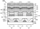
fig. 18A and 18B are a top view and a cross-sectional view illustrating a display device according to one embodiment of the present invention;
fig. 19A and 19B are schematic cross-sectional views illustrating a display device according to an embodiment of the present invention;
fig. 20 is a schematic cross-sectional view illustrating a display device according to an embodiment of the present invention;
fig. 21A and 21B are schematic cross-sectional views illustrating a display device according to an embodiment of the present invention;
fig. 22A and 22B are schematic cross-sectional views illustrating a display device according to an embodiment of the present invention;
fig. 23 is a schematic cross-sectional view illustrating a display device according to an embodiment of the present invention;
fig. 24A and 24B are schematic cross-sectional views illustrating a display device according to an embodiment of the present invention;
fig. 25 is a schematic cross-sectional view illustrating a display device according to an embodiment of the present invention;
Fig. 26A and 26B are schematic cross-sectional views illustrating a display device according to an embodiment of the present invention;
fig. 27A to 27D are schematic cross-sectional views illustrating a method of manufacturing an EL layer;
fig. 28 is a schematic view illustrating a liquid droplet ejection apparatus;
fig. 29A and 29B are a block diagram and a circuit diagram illustrating a display device according to one embodiment of the present invention;
fig. 30A and 30B are circuit diagrams illustrating a pixel circuit according to an embodiment of the present invention;
fig. 31A and 31B are circuit diagrams illustrating a pixel circuit according to one embodiment of the present invention;
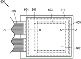
fig. 32A and 32B are perspective views showing an example of a touch panel according to an embodiment of the present invention;
fig. 33A to 33C are cross-sectional views showing examples of a display device and a touch sensor according to an embodiment of the present invention;
fig. 34A and 34B are cross-sectional views showing an example of a touch panel according to an embodiment of the present invention;
fig. 35A and 35B are a block diagram and a timing chart of a touch sensor according to an embodiment of the present invention;
fig. 36 is a circuit diagram of a touch sensor according to an embodiment of the present invention;
fig. 37 is a perspective view of a display module illustrating one mode of the present invention;
fig. 38A to 38G are diagrams illustrating an electronic device according to an embodiment of the present invention;
Fig. 39A to 39D are diagrams illustrating an electronic device according to an embodiment of the present invention;
fig. 40A and 40B are perspective views illustrating a display device according to one embodiment of the present invention;
fig. 41A to 41C are a perspective view and a sectional view illustrating a light-emitting device according to an embodiment of the present invention;
fig. 42A to 42D are sectional views illustrating a light-emitting device according to an embodiment of the present invention;
fig. 43A to 43C are diagrams illustrating a lighting device and an electronic apparatus according to an embodiment of the present invention;
fig. 44 is a diagram illustrating a lighting device according to an embodiment of the present invention;
FIG. 45 is an absorption spectrum and an emission spectrum of a solution and a thin film of the example;
FIG. 46 is an absorption spectrum and an emission spectrum of a solution and a thin film of the example;
FIG. 47 shows absorption spectra and emission spectra of the solution and the thin film of the example.
Detailed Description
Hereinafter, embodiments of the present invention will be described in detail with reference to the drawings. Note that the present invention is not limited to the following description, and the mode and the details thereof may be changed into various forms without departing from the spirit and the scope of the present invention. Therefore, the present invention should not be construed as being limited to the description of the embodiments shown below.
For convenience of understanding, the positions, sizes, ranges, and the like of the respective components shown in the drawings and the like do not indicate actual positions, sizes, ranges, and the like. Accordingly, the disclosed invention is not necessarily limited to the positions, sizes, ranges, etc., disclosed in the drawings and the like.
Note that, in this specification and the like, first and second ordinal numbers are added for convenience, and they do not sometimes indicate the order of steps or the order of stacking. Therefore, for example, "first" may be appropriately replaced with "second" or "third" and the like. In addition, ordinal numbers described in this specification and the like may not coincide with ordinal numbers for specifying one embodiment of the present invention.
Note that in this specification and the like, when the structure of the invention is described with reference to the drawings, symbols indicating the same parts may be used in common in different drawings.
In this specification and the like, "film" and "layer" may be interchanged with each other. For example, the "conductive layer" may be sometimes referred to as a "conductive film". Further, the "insulating film" may be sometimes referred to as an "insulating layer".
In addition, in the present specification and the like, singlet excited state (S) *) Refers to a singlet state with excitation energy. The S1 level is the lowest level of the singlet excited levels, i.e., the excited level of the lowest singlet excited state. In addition, triplet excited state (T)*) Refers to a triplet state having excitation energy. The T1 level is the lowest level of the triplet excited level, that is, the excited level of the lowest triplet excited state.
In the present specification and the like, the fluorescent compound refers to a compound that emits light in the visible light region when returning from a singlet excited state to a ground state. The phosphorescent compound refers to a compound that emits light in a visible light region at room temperature when returning from a triplet excited state to a ground state. In other words, the phosphorescent compound refers to one of compounds capable of converting triplet excitation energy into visible light.
In the present specification and the like, the emission energy of the thermally activated delayed fluorescence refers to an emission peak (including a shoulder peak) on the shortest wavelength side of the thermally activated delayed fluorescence. The phosphorescence emission energy or triplet excited state energy refers to a phosphorescence emission peak (including a shoulder peak) on the shortest wavelength side of phosphorescence emission. In addition, the above-mentioned phosphorescence can be observed by a time-resolved photoluminescence spectrum in a low temperature (e.g., 10K) environment.
In the present specification and the like, room temperature means any temperature of 0 ℃ to 40 ℃.
In the present specification and the like, the wavelength region of blue refers to a wavelength region of 400nm or more and less than 490nm, and blue light emission is light emission having at least one emission spectrum peak in the wavelength region. The wavelength region of green is a wavelength region of 490nm or more and less than 580nm, and green light emission is light emission having at least one emission spectrum peak in the wavelength region. The red wavelength region is a wavelength region of 580nm to 680nm inclusive, and the red emission is an emission having at least one emission spectrum peak in the wavelength region.
In this embodiment, a light-emitting element which is one embodiment of the present invention will be described with reference to fig. 1A to 10D.
Structure example of light emitting element
First, a structure of a light-emitting element which is one mode of the present invention will be described below with reference to fig. 1A to 1C.
Fig. 1A is a schematic cross-sectional view of a light-emitting element 150 according to one embodiment of the present invention.
The light-emitting element 150 includes a pair of electrodes (an electrode 101 and an electrode 102), and includes an EL layer 100 provided between the pair of electrodes. The EL layer 100 includes at least a light emitting layer 130.
The EL layer 100 shown in fig. 1A includes functional layers such as a hole injection layer 111, a hole transport layer 112, an electron transport layer 118, and an electron injection layer 119 in addition to the light-emitting layer 130.
Note that although the description is given in this embodiment mode with the electrode 101 as an anode and the electrode 102 as a cathode in a pair of electrodes, the structure of the light-emitting element 150 is not limited to this. That is, the layers between the electrodes may be stacked in reverse order using the electrode 101 as a cathode and the electrode 102 as an anode. In other words, the hole injection layer 111, the hole transport layer 112, the light-emitting layer 130, the electron transport layer 118, and the electron injection layer 119 may be stacked in this order from the anode side.
Note that the structure of the EL layer 100 is not limited to the structure shown in fig. 1A as long as at least one selected from the group consisting of the hole injection layer 111, the hole transport layer 112, the electron transport layer 118, and the electron injection layer 119 is included. Alternatively, the EL layer 100 may include functional layers having the following functions: an injection barrier capable of reducing holes or electrons; the hole or electron transport property can be improved; ability to block hole or electron transport; or quenching phenomenon caused by the electrode can be suppressed. The functional layer may be a single layer or a structure in which a plurality of layers are stacked.
Fig. 1B is a schematic cross-sectional view illustrating an example of the light-emitting layer 130 illustrated in fig. 1A. The light-emitting layer 130 shown in fig. 1B includes a host material 131 and a guest material 132.
As the guest material 132, a light-emitting organic compound may be used, and as the light-emitting organic compound, a substance capable of emitting fluorescence (hereinafter, also referred to as a fluorescent compound) is preferably used. In the following description, a structure in which a fluorescent compound is used as the guest material 132 will be described. Note that the guest material 132 may also be referred to as a fluorescent compound.
In the light-emitting element 150 according to one embodiment of the present invention, a voltage is applied between a pair of electrodes (the electrode 101 and the electrode 102), and electrons and holes are injected into the EL layer 100 from the cathode and the anode, respectively, whereby a current flows. The injected electrons and holes are recombined to form excitons. Among excitons generated by recombination of carriers (electrons and holes), the statistical probability of the ratio of singlet excitons to triplet excitons (hereinafter referred to as exciton generation probability) is 1: 3. Therefore, in a light-emitting element using a fluorescent compound, the ratio of singlet excitons which contribute to light emission is 25%, and the ratio of triplet excitons which do not contribute to light emission is 75%. Therefore, in order to improve the light emission efficiency of the light-emitting element, it is important to convert triplet excitons that do not contribute to light emission into singlet excitons that contribute to light emission.
Thus, the host material 131 preferably has a function of generating a singlet excited state from a triplet excited state.
Light emitting mechanism of light emitting element
Next, the light emission mechanism of the light emitting layer 130 will be explained below.
The host material 131 in the light-emitting layer 130 preferably includes a skeleton having a function of transporting holes (hole-transporting property) and a skeleton having a function of transporting electrons (electron-transporting property). Alternatively, the host material 131 preferably includes at least one of a pi-electron-rich type heteroaromatic skeleton and an aromatic amine skeleton and has a pi-electron-deficient type heteroaromatic skeleton.
In one embodiment of the present invention, the host material 131 is a material having the following functions: an excited complex (also referred to as an excited dimer) is formed with two molecules of the host material 131 having the same molecular structure. Among them, the skeleton having a hole-transporting property of the host material 131 and the skeleton having an electron-transporting property of the host material 131 preferably form an excited complex in two molecules having the same molecular structure. Alternatively, at least one of the pi-electron-rich heteroaromatic skeleton and the aromatic amine skeleton in the host material 131 and the pi-electron-deficient heteroaromatic skeleton in the host material 131 preferably form an excited complex in two molecules having the same molecular structure. Note that the excited complex is formed in an excited state by two molecules having the same molecular structure, but it is important to form a charge transfer type excited state unlike a general excited dimer (also referred to as an excimer). That is, while an excited state is formed by two molecules having the same molecular structure, an excited state in which one molecule is positively charged and the other molecule is negatively charged is present. Note that in this specification and the like, "molecules having the same molecular structure" means molecules that can be represented by the same structural formula, and the bonding direction, bonding angle, bonding length, and the like of atoms and skeletons of the molecules may be different. The "molecules having the same molecular structure" may be geometric isomers, stereoisomers, optical isomers, and the like.
In other words, the host material 131 is a material having a function of forming an excited complex with a first molecule and a second molecule of the host material 131. Among them, in the host material 131, the skeleton having a hole-transporting property in the first molecule and the skeleton having an electron-transporting property in the second molecule preferably form an excited complex. Alternatively, in the host material 131, at least one of the pi-electron-rich heteroaromatic skeleton and the aromatic amine skeleton in the first molecule and the pi-electron-deficient heteroaromatic skeleton in the second molecule preferably form an excited complex.
When the host material 131 includes a skeleton having a hole-transporting property and a skeleton having an electron-transporting property, a donor-acceptor type excited complex is easily formed from two molecules, and an excited complex can be efficiently formed. Alternatively, when the host material 131 has at least one of a pi-electron-rich heteroaromatic skeleton and an aromatic amine skeleton and a pi-electron-deficient heteroaromatic skeleton, a donor-acceptor type excited complex is easily formed from two molecules, and an excited complex can be efficiently formed.
Accordingly, the host material 131 preferably has a structure in which the conjugation between the skeleton having a hole-transporting property and the skeleton having an electron-transporting property is reduced so that both donor and acceptor can be enhanced in the molecule. Alternatively, it is preferable to have a structure in which the conjugation of at least one of the pi-electron-rich type heteroaromatic skeleton and the aromatic amine skeleton with the pi-electron-deficient type heteroaromatic skeleton is reduced. By having the above structure, the overlap of the region of the Highest Occupied Molecular Orbital (HOMO) distribution and the region of the Lowest Unoccupied Molecular Orbital (LUMO) distribution can be made small. In addition, the difference between the singlet excitation level and the triplet excitation level of the host material 131 can be made small. Further, the triplet excitation energy of the host material 131 can be made high.
Note that the "molecular trajectory" may show the spatial distribution of electrons in a molecule and the probability of the electrons. The electronic configuration (spatial distribution and energy of electrons) of a molecule can be described in detail by molecular orbitals.
Since the excited complex has a HOMO in one molecule and a LUMO in another molecule, the overlap of the HOMO and the LUMO of the excited complex formed by two molecules having the same structure is extremely small. That is, in the excited complex, the difference between the singlet excitation level and the triplet excitation level is small. Thus, in the excited complex formed by two molecules in the host material 131, the difference between the singlet excitation level and the triplet excitation level is small, and the difference is preferably more than 0eV and 0.2eV or less.
When the host material 131 includes a skeleton having a hole-transporting property and a skeleton having an electron-transporting property, the balance of carriers can be easily controlled. Thereby, the carrier recombination region can be easily controlled.
Here, fig. 1C shows that the energy levels of the host material 131 and the guest material 132 in the light-emitting layer 130 are related. Note that the description and notation in fig. 1C are as follows:
host (131): host material 131
Guest (132): guest material 132 (fluorescent compound)
·SH: s1 energy level of host material 131
·TH: t1 energy level of host material 131
·SG: s1 energy level of guest material 132 (fluorescent compound)
·TG: t1 energy level of guest material 132 (fluorescent compound)
·SE: s1 energy level of excited complex
·TE: t1 energy level of excited complex
In the light-emitting element according to one embodiment of the present invention, an excited complex is formed from two molecules in the host material 131 included in the light-emitting layer 130. Lowest singlet excitation level (S) of excited complexesE) Lowest triplet excitation level (T) with excited complexE) Are adjacent to each other (see path E of FIG. 1C)3)。
An excited complex is an excited state formed by two molecules, and in the case of photoexcitation, an excited complex is formed by the interaction of one molecule in the excited state with another molecule in the ground state. When returning to the ground state by emitting light, the two molecules forming the excited complex respectively return to the original molecular states. In the case of electrical excitation, when one molecule is in an excited state, it rapidly interacts with another molecule to form an excited complex. Alternatively, the excited complex can be rapidly formed by having one molecule accept a hole and the other molecule accept an electron. At this time, the excited complex may be formed in such a manner that a single molecule does not form an excited state in any molecule, so most of excitons in the light-emitting layer 130 may exist as the excited complex . Excitation level (S) of excited complexEAnd TE) A singlet excitation level (S) of a single molecule of the host material 131 forming an excited complexH) Low, the excited state of the host material 131 can be formed with lower excitation energy. This can reduce the driving voltage of the light-emitting element 150.
Due to the singlet excitation level (S) of the excited complexE) With triple excitation level (T)E) Are adjacent energy levels and thus have the function of exhibiting thermally activated delayed fluorescence. That is, the excited complex has a function of converting triplet excited state energy into singlet excited state energy by intersystem crossing (upconversion). (refer to Path E of FIG. 1C4). Therefore, a part of triplet excitation energy generated in the light emitting layer 130 is converted into singlet excitation energy by the excited complex. For this purpose, the singlet excitation level (S) of the excited complexE) With triple excitation level (T)E) The energy difference of (b) is preferably more than 0eV and 0.2eV or less.
In addition, the singlet excitation level (S) of the excited complexE) Preferably above the singlet excitation level (S) of guest material 132G). Thus, the singlet excitation energy of the excited complex generated can be derived from the singlet excitation level (S) of the excited complexE) Transferred to the singlet excitation level (S) of the guest material 132 G). As a result, the guest material 132 enters a singlet excited state and emits light (see path E in fig. 1C)5)。
In order to efficiently obtain light emission from the singlet excited state of the guest material 132, the fluorescence quantum yield of the guest material 132 is preferably high, specifically, 50% or more, more preferably 70% or more, and still more preferably 90% or more.
Note that, in order to efficiently generate the intersystem crossing, the triplet excitation level (T) of the excited complex formed by two moleculesE) Preferably below the triplet excitation level (T) of a single molecule of the host material 131 forming the excited complexH). Thus, quenching of triplet excitation energy of an excited complex formed by molecules other than the molecules forming the excited complex in the host material 131 is not easily generated, and intersystem crossing is efficiently generated。
In order to achieve the above, it is preferable that the triplet excitation level of the host material 131 is high and the energy difference between the singlet excitation level and the triplet excitation level of the host material 131 is small.
Since the direct transition from the singlet ground state to the triplet excited state in the guest material 132 is a forbidden transition, the singlet excited level (S) from the excited complexE) Triplet excitation level (T) to guest material 132 G) The energy transfer of (a) is not easily a major energy transfer process.
In addition, when a triplet excitation level (T) from the excited complex occursE) Triplet excitation level (T) to guest material 132G) Upon transfer of the triplet excitation energy of (2), the triplet excitation energy is deactivated (see path E in FIG. 1C)6). Thus, path E6The energy transfer of (a) is preferably less likely to occur so that the generation efficiency of the triplet excited state of the guest material 132 can be reduced and thermal deactivation can be reduced. For this reason, the proportion of the guest material 132 is preferably low in the weight ratio of the host material 131 to the guest material 132, and specifically, the weight ratio of the guest material 132 to the host material 131 is preferably 0.001 or more and 0.05 or less, more preferably 0.001 or more and 0.03 or less, and further preferably 0.001 or more and 0.01 or less.
Note that when a direct recombination process of carriers in the guest material 132 is dominant, a plurality of triplet excitons are generated in the light emitting layer 130, and thermal deactivation causes a decrease in light emitting efficiency. Therefore, it is preferable that the energy transfer process is via the generation process of the excited complex (path E of FIG. 1C)4And E5) The ratio of (b) is higher than that of a process in which carriers in the guest material 132 are directly recombined, because the generation efficiency of triplet excited states of the guest material 132 can be reduced and thermal deactivation can be suppressed. For this reason, the proportion of the guest material 132 is low in the weight ratio of the host material 131 to the guest material 132, and specifically, the weight ratio of the guest material 132 to the host material 131 is preferably 0.001 or more and 0.05 or less, more preferably 0.001 or more and 0.03 or less, and further preferably 0.001 or more and 0.01 or less.
As described above, whenThe above path E4And E5When all the energy transfer processes of (a) are efficiently performed, both the singlet excitation energy and the triplet excitation energy of the host material 131 are efficiently converted into the singlet excitation energy of the guest material 132, and thus the light-emitting element 150 can emit light with high emission efficiency.
The excited complex may be referred to as an exciplex (exiplex), and therefore, in this specification and the like, the above-mentioned route E may be referred to as an exciplex3、E4And E5The process of (2) is called ExSET (Exciplex-Singlet Energy Transfer: Exciplex-Singlet Energy Transfer) or ExEF (Exciplex-Enhanced Fluorescence: Exciplex-Enhanced Fluorescence). In other words, in the light-emitting layer 130, supply of excitation energy from the excited complex to the guest material 132 is generated.
By providing the light-emitting layer 130 with the above structure, light emission from the guest material 132 of the light-emitting layer 130 can be efficiently obtained.
In addition, as a material having a function of generating a singlet excited state from a triplet excited state, a Thermally Activated Delayed Fluorescence (TADF) material is known. The TADF material is a material which can generate a singlet excited state from a triplet excited state by intersystem crossing and exhibit light emission from the singlet excited state when the material is used alone. That is, the TADF material is a material capable of converting a part of triplet excited state energy into light emission.
Thus, in the TADF material, the difference between the triplet excited state level and the singlet excited state level is small, and the triplet excited state can be up-converted to the singlet excited state with a slight thermal energy. Specifically, the difference between the triplet excited state level and the singlet excited state level is preferably greater than 0eV and 0.2eV or less, more preferably greater than 0eV and 0.1eV or less.
Examples of the TADF material include heterocyclic compounds having a pi-electron-rich heteroaromatic skeleton and a pi-electron-deficient heteroaromatic skeleton. In order to impart the function of thermally-activated delayed fluorescence to the heterocyclic compound, it is preferable that the donor of the pi-electron-rich heteroaromatic skeleton and the acceptor of the pi-electron-deficient heteroaromatic skeleton are enhanced by directly bonding the pi-electron-rich heteroaromatic skeleton and the pi-electron-deficient heteroaromatic skeleton to each other. Further, it is preferable that the overlap of the HOMO and the LUMO is small by reducing the conjugation of the pi-electron-rich heteroaromatic skeleton and the pi-electron-deficient heteroaromatic skeleton. On the other hand, when there is a certain degree of overlap between the HOMO and LUMO, it is preferable to increase the transition probability (oscillator strength) between the HOMO and LUMO. This makes it possible to obtain light emission from a singlet excited state efficiently while reducing the difference between the singlet excited state level and the triplet excited state level.
Examples of structures suitable for these heterocyclic compounds include pi-electron-rich heteroaromatic skeletons such as acridine skeleton, phenazine skeleton, and phenoxazine skeleton, and the skeletons have the following structures: has a strong twist at a site bonded to the pi-electron-deficient heteroaromatic skeleton, and reduces conjugation of the pi-electron-rich heteroaromatic skeleton and the pi-electron-deficient heteroaromatic skeleton. However, the skeleton having these twisted structures has a limitation on the molecular structure.
In one embodiment of the present invention, the host material 131 is preferably made of: the skeleton having a hole-transporting property is bonded to the skeleton having an electron-transporting property via a structure having at least one of m-phenylene group and o-phenylene group. In the above structure having at least one of m-phenylene and o-phenylene, it is particularly preferable that at least one of m-phenylene and o-phenylene is bonded to the arylene group. By adopting the above structure, the HOMO orbital within the molecule is physically (distance) separated from the LUMO orbital. As a result, the formation of the excited complex (for example, electron transfer between the HOMO of the first molecule and the LUMO of the second molecule) is more dominant than the formation of an excited complex in a charge transfer type excited state in a molecule (based on the HOMO-LUMO transfer in a molecule), and thus is suitable for one embodiment of the present invention. For the same reason, in the host material 131, it is particularly preferable that a skeleton having a hole-transporting property is bonded to a skeleton having an electron-transporting property through a biphenyldiyl group.
In addition, the host material 131 is preferably the following material: at least one of the pi-electron-rich heteroaromatic skeleton and the aromatic amine skeleton is bonded to the pi-electron-deficient heteroaromatic skeleton via a structure having at least one of m-phenylene and o-phenylene. In the above structure having at least one of m-phenylene and o-phenylene, it is particularly preferable that at least one of m-phenylene and o-phenylene is bonded to the arylene group. By adopting the above structure, the HOMO orbital within the molecule is physically (distance) separated from the LUMO orbital. As a result, the formation of the excited complex (for example, electron transfer between the HOMO of the first molecule and the LUMO of the second molecule) is more dominant than the formation of a charge transfer type excited state in the excited complex molecule (based on the intra-molecular HOMO-LUMO transfer), and thus is suitable for one embodiment of the present invention. For the same reason, in the host material 131, it is particularly preferable that at least one of the pi-electron-rich heteroaromatic skeleton and the aromatic amine skeleton is bonded to the pi-electron-deficient heteroaromatic skeleton via a biphenyldiyl group.
Energy level and molecular orbital calculation using quantum chemistry
Next, as an example of a compound that can be used for the host material 131 in one embodiment of the present invention, an energy level is calculated by quantum chemistry.
The structures and abbreviations of the compounds used for the calculations are shown below. In addition, tables 1 to 3 show the calculated S1 energy level, T1 energy level, and energy difference (Δ S1-T1) between the S1 energy level and the T1 energy level in the most stable structure of each compound.
[ chemical formula 1]

[ chemical formula 2]

[ chemical formula 3]

[ Table 1]
| For short | S1 energy level [ eV] | T1 level [ eV] | ΔS1-T1[eV] |
| 2DPhAPDBq | 2.90 | 2.38 | 0.52 |
| 2mDPhAPDBq | 2.77 | 2.55 | 0.22 |
| 2DPhABPDBq | 2.82 | 2.45 | 0.38 |
| 2pmDPhABPDBq | 2.84 | 2.60 | 0.24 |
| 2mpDPhABPDBq | 2.81 | 2.66 | 0.15 |
| 2mDPhABPDBq | 2.85 | 2.70 | 0.14 |
[ Table 2]
| For short | S1 energy level [ eV] | T1 level [ eV] | ΔS1-T1[eV] |
| 4DPhAPPm | 3.13 | 2.54 | 0.59 |
| 4mDPhAPPm | 2.86 | 2.59 | 0.27 |
| 4DPhABPPm | 2.94 | 2.52 | 0.42 |
| 4pmDPhABPPm | 2.91 | 2.71 | 0.20 |
| 4mpDPhABPPm | 2.92 | 2.73 | 0.19 |
| 4mDPhABPPm | 2.95 | 2.90 | 0.05 |
[ Table 3]
| For short | S1 energy level [ eV] | T1 level [ eV] | ΔS1-T1[eV] |
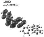
| 4CzPBfpm | 2.95 | 2.62 | 0.33 |
| 4mCzBPBfpm | 3.01 | 2.93 | 0.08 |
The calculation method is as follows. As a quantum chemical calculation program, Gaussian09 was used. The calculation was performed using a high performance computer (ICE X, SGI corporation).
First, the most stable structure in the ground singlet state is calculated by the density functional method (DFT). 6-311G (d, p) was used as the basis function. B3LYP was used as a generic function. Next, the energy at which the transition from the most stable structure in the singlet ground state to the singlet excited state and the triplet excited state occurs is calculated by the time-dependent density functional method (TD-DFT). All energies of DFT are expressed as the sum of potential energy, electrostatic energy between electrons, kinetic energy of electrons, exchange-related energy including all other complex interactions between electrons. In DFT, the cross-correlation effect is approximated by a functional (function of function) of a one-electron potential expressed by an electron density, and therefore, the calculation accuracy is high.
The chemical represented by chemical formula 1 has dibenzo [ f, h ] quinoxaline (abbreviated as DBq) lacking a pi-electron type heteroaromatic skeleton and triphenylamine (abbreviated as TPA) having an aromatic amine skeleton. In addition, the chemical represented by chemical formula 2 has 4, 6-diphenylpyrimidine lacking a pi-electron type heteroaromatic skeleton (abbreviated as P2Pm) and TPA of an aromatic amine skeleton. In addition, the chemical represented by chemical formula 3 has benzofuro [3, 2-d ] pyrimidine (abbreviated as Bfpm) having a pi-electron deficient heteroaromatic skeleton and 9-phenyl-9H-carbazole (abbreviated as PCz) having a pi-electron rich heteroaromatic skeleton.
As shown in chemical formula 1 and Table 1, 4- (dibenzo [ f, h ] quinoxalin-2-yl) triphenylamine (abbreviated as 2DPhAPDBq) has p-phenylene group, and the energy difference between the S1 level and the T1 level is large. Thus, the T1 energy level is relatively low. On the other hand, 3- (dibenzo [ f, h ] quinoxalin-2-yl) triphenylamine (abbreviated as 2mDPhAPDBq) has m-phenylene group, and the energy difference between the S1 energy level and the T1 energy level is smaller than 2 DPhAPDBq. N, N-diphenyl-N- [4- (dibenzo [ f, h ] quinoxalin-2-yl) phenyl ] phenyl-4-amine (2 DPhABBPDBq for short) has a biphenyldiyl group, and the energy difference between the S1 level and the T1 level is smaller than that of 2 DPhAPDBq. N, N-diphenyl-N- [4- (dibenzo [ f, h ] quinoxalin-2-yl) phenyl ] phenyl-3-amine (abbreviated as 2 pmDPhABBPDBq), N-diphenyl-N- [3- (dibenzo [ f, h ] quinoxalin-2-yl) phenyl ] phenyl-4-amine (abbreviated as 2 mpDPhABBPDBq) and N, N-diphenyl-N- [3- (dibenzo [ f, h ] quinoxalin-2-yl) phenyl ] phenyl-3-amine (abbreviated as 2 mdDPhABBPq) have a biphenyl diyl group containing a m-phenylene group, and the energy difference between the S1 level and the T1 level is smaller than that of 2 DPhABDBq and 2 DPhABBPq. Among them, when a biphenyldiyl group including two m-phenylene groups is present as in 2 mdphabbpdbq, the energy difference between the S1 level and the T1 level is small, that is, larger than 0eV and not more than 0.2eV, and thus it is preferable. As can be seen from table 1, the smaller the energy difference between the S1 energy level and the T1 energy level, the higher the T1 energy level is relatively. As described later, since the T1 level of a single molecule becomes high and the T1 level of the excited complex becomes more stable than that of a single molecule, this is suitable for the structure of the present invention.
As shown in chemical formula 2 and Table 2, N, N-diphenyl-N- (4-phenyl-pyrimidin-6-yl) phenyl-4-amine (4 DPhAPm) has p-phenylene group, and the energy difference between the S1 level and the T1 level is large. Thus, the T1 energy level is relatively low. On the other hand, N, N-diphenyl-N- (4-phenyl-pyrimidin-6-yl) phenyl-3-amine (4 mDPhAPm for short) has a meta-phenylene group, and the energy difference between the S1 level and the T1 level is smaller than that of 4 DPhAPm. N, N-diphenyl-N- [4- (4-phenyl-pyrimidin-6-yl) phenyl ] phenyl-4-amine (4 DPhABPP) has a biphenyldiyl group, and the energy difference between the S1 level and the T1 level is smaller than 4 DPhAPm. N, N-diphenyl-N- [4- (4-phenyl-pyrimidin-6-yl) phenyl ] phenyl-3-amine (abbreviated: 4 pmDPhABPm), N-diphenyl-N- [3- (4-phenyl-pyrimidin-6-yl) phenyl ] phenyl-4-amine (abbreviated: 4 mpDPhABPm) and N, N-diphenyl-N- [3- (4-phenyl-pyrimidin-6-yl) phenyl ] phenyl-3-amine (abbreviated: 4 mDPhABPm) have a biphenyl diyl group containing an m-phenylene group, and the energy difference between the S1 level and the T1 level is smaller than that of 4 DPhABPm and 4 DPhABPm. Among them, when a biphenyldiyl group including two m-phenylene groups is present as in 4 mdphabbppm, the energy difference between the S1 level and the T1 level is particularly small, that is, 0.1eV or less, and therefore, it is preferable. As can be seen from table 2, the smaller the energy difference between the S1 energy level and the T1 energy level, the higher the T1 energy level is relatively. As described later, since the T1 level of a single molecule becomes high and the T1 level of the excited complex becomes more stable than that of a single molecule, this is suitable for the structure of the present invention.
As shown in chemical formula 3 and Table 3, 4- {3- [ 3' - (9H-carbazol-9-yl) ] biphenyl-3-yl } benzofuro [3, 2-d ] pyrimidine (abbreviated as 4mCzBPBfpm) has biphenyl diyl group containing m-phenylene group, and the energy difference between S1 level and T1 level is smaller than that of 4- [4- (9H-carbazol-9-yl) phenyl ] benzofuro [3, 2-d ] pyrimidine (abbreviated as 4CzPBfpm) containing p-phenylene group, that is, 0.1eV or less, and thus is preferable. As can be seen from table 3, the smaller the energy difference between the S1 energy level and the T1 energy level, the higher the T1 energy level is relatively. As described later, since the T1 level of a single molecule becomes high and the T1 level of the excited complex becomes more stable than that of a single molecule, this is suitable for the structure of the present invention.
As described above, the host material 131 according to one embodiment of the present invention is preferably made of: at least one of the pi-electron-rich heteroaromatic skeleton and the aromatic amine skeleton is bonded to the pi-electron-deficient heteroaromatic skeleton via a structure having at least one of m-phenylene and o-phenylene. Alternatively, at least one of the pi-electron-rich heteroaromatic skeleton and the aromatic amine skeleton is preferably bonded to the pi-electron-deficient heteroaromatic skeleton via a biphenyldiyl group having at least one of a m-phenylene group and an o-phenylene group.
Next, the energy level and the molecular orbital of the excited complex (excited dimer) are calculated by quantum chemical calculation.
First, a calculation is made for a compound having a pi-electron deficient heteroaromatic skeleton, a pi-electron rich heteroaromatic skeleton or an aromatic amine skeleton. Next, the excited complex (excited dimer) formed by combining two of the above-described compounds was calculated. The structures and abbreviations of the individual compounds used for the calculations are shown below. Table 4 and table 5 show the calculated HOMO level, LUMO level, S1 level, T1 level, and energy difference (Δ S1 to T1) between the S1 level and the T1 level of the single compound and the excited complex formed by combining two compounds among the above compounds.
[ chemical formula 4]

[ Table 4]

[ Table 5]

The calculation method is as follows. First, the optimum molecular structures in the lowest singlet excited state and the lowest triplet excited state of a single DBq having a pi-electron-deficient heteroaromatic skeleton, a single P2Pm and a single Bfpm, a single TPA having an aromatic amine skeleton, and a single PCz having a pi-electron-rich heteroaromatic skeleton were calculated, and the excitation level and the molecular orbital thereof were calculated by a time-dependent density functional method (TD-DFT). Further, the excited complex formed by TPA and DBq, the excited complex formed by TPA and P2Pm, and the excited complex formed by PCz and Bfpm were calculated in the same manner as described above. 6-311G (d, p) was used as the basis function. B3LYP was used as a generic function.
Fig. 2A to 2F and fig. 4A to 4D show the calculated distributions of HOMO and LUMO of individual molecules of the compounds. FIGS. 2A and 2B show the HOMO and LUMO distributions of a single TPA. Fig. 2C and 2D show HOMO and LUMO distributions for a single DBq. FIGS. 2E and 2F show the HOMO and LUMO distributions for a single P2 Pm. Fig. 4A and 4B show the HOMO and LUMO distributions of a single PCz. Fig. 4C and 4D show the HOMO and LUMO distributions of a single Bfpm.
The distributions of HOMO and LUMO of the single TPA, the distributions of HOMO and LUMO of the single DBq, the distributions of HOMO and LUMO of the single P2Pm, the distributions of HOMO and LUMO of the single PCz, and the distributions of HOMO and LUMO of the single Bfpm have regions that substantially overlap each other. Thus, as shown in table 4, the energy difference between the S1 level and the T1 level of these compounds is large, i.e., 0.5eV or more.
Next, fig. 3A to 3D and fig. 4E and 4F show the calculated distributions of HOMO and LUMO of the excited complex formed by TPA and DBq, the distributions of HOMO and LUMO of the excited complex formed by TPA and P2Pm, and the distributions of HOMO and LUMO of the excited complex formed by PCz and Bfpm. FIGS. 3A and 3B show the HOMO and LUMO distributions of excited complexes formed by TPA and DBq. FIGS. 3C and 3D show the HOMO and LUMO distributions of excited complexes formed by TPA and P2 Pm. Fig. 4E and 4F show distributions of HOMO and LUMO of PCz with an excited complex formed with Bfpm.
As shown in table 4, table 5, and fig. 3A and 3B, the HOMO of the excited complex formed by TPA and DBq is distributed on TPA having a higher HOMO level than DBq, and the LUMO is distributed on DBq having a lower LUMO level than TPA. Thus, the HOMO level of the excited complex formed by TPA and DBq approaches the HOMO level of TPA, and the LUMO level of the excited complex approaches the LUMO level of DBq. That is, TPA forms excited complexes of HOMO on TPA and LUMO on DBq with DBq. The S1 energy level and the T1 energy level of the excited complex are lower than the S1 energy level and the T1 energy level of single TPA and single DBq, and stabilization is realized. In addition, TPA forms excited complexes with DBq with minimal overlap of HOMO and LUMO. Accordingly, the energy difference between the S1 level and the T1 level of the excited complex formed by TPA and DBq is extremely small, that is, 0.01eV or less.
As shown in table 4, table 5, and fig. 3C and 3D, the HOMO of the excited complex formed by TPA with P2Pm was distributed on TPA having a higher HOMO level than P2Pm, and the LUMO was distributed on P2Pm having a lower LUMO level than TPA. Thus, the HOMO level of the excited complex of TPA with P2Pm approaches that of TPA, and the LUMO level of the excited complex approaches that of P2 Pm. That is, TPA forms an excited complex of HOMO on TPA and LUMO on DBq with P2 Pm. The S1 energy level and the T1 energy level of the excited complex are lower than the S1 energy level and the T1 energy level of single TPA and single P2Pm, and stabilization is realized. In addition, TPA forms an excited complex with P2Pm with minimal overlap of HOMO and LUMO. Thus, the energy difference between the S1 level and the T1 level of the excited complex formed between TPA and P2Pm is extremely small, i.e., 0.01eV or less.
As shown in table 4, table 5, and fig. 4E and 4F, the HOMO of the excited complex formed with Bfpm at PCz was distributed at PCz having a HOMO level higher than Bfpm, and the LUMO was distributed at Bfpm having a LUMO level lower than PCz. Thus, PCz forms an excited complex with Bfpm, which has a HOMO level close to PCz and a LUMO level close to Bfpm. That is, PCz forms an excited complex with Bfpm of HOMO at PCz and LUMO at Bfpm. The excited complex has S1 energy level and T1 energy level lower than single PCz energy level and single Bfpm S1 energy level and T1 energy level, and realizes stabilization. In addition, PCz showed minimal overlap of HOMO and LUMO with the excited complex formed by Bfpm. Thus, the energy difference between the S1 level and the T1 level of the excited complex formed by PCz and Bfpm is extremely small, that is, 0.01eV or less.
Next, with respect to 2DPhAPDBq, 2 mdphbpdbq, 4DPhAPPm, 4 mdphbppm, 4CzPBfpm, and 4mCzBPBfpm among the compounds represented by chemical formulas 1 to 3, in order to verify whether excited complexes (charge transfer type excited dimers) are formed by two molecules having the same structure, the energy levels and molecular orbitals of these excited complexes were calculated by quantum chemical calculation. Table 6 shows the S1 energy level, the T1 energy level, and the energy difference between the S1 energy level and the T1 energy level (Δ S1-T1) of the excited complex. In addition, the calculation method is as follows: and (3) calculating the optimal molecular structure in the lowest singlet excited state and the lowest triplet excited state, and calculating the excited level and the molecular orbit of the molecular structure by using a time-dependent density functional method (TD-DFT). 6-311G (d, p) was used as the basis function, and B3LYP was used as the generic function.
[ Table 6]

Fig. 5A to 10D show the calculated HOMO and LUMO distributions. Fig. 5A and 5B show the HOMO and LUMO distributions of a single 2 DPhAPDBq. Fig. 5C and 5D show distributions of HOMO and LUMO of excited complexes (excited dimers) formed by two 2 DPhAPDBq. Fig. 6A and 6B show the HOMO and LUMO distributions of a single 2 mdphabdbq. Fig. 6C and 6D show distributions of HOMO and LUMO of an excited complex (excited dimer) formed by two molecules of 2 mdphabdbq. Fig. 7A and 7B show HOMO and LUMO distributions of a single 4 DPhAPPm. Fig. 7C and 7D show distributions of HOMO and LUMO of an excited complex (excited dimer) formed by two molecules of 4 DPhAPPm. Fig. 8A and 8B show the HOMO and LUMO distributions of a single 4 mdphbppm. Fig. 8C and 8D show the HOMO and LUMO distributions of two excited complexes (excited dimers) formed by 4 mdphabpm. Fig. 9A and 9B show the HOMO and LUMO distributions of a single 4 CzPBfpm. Fig. 9C and 9D show distributions of HOMO and LUMO of an excited complex (excited dimer) formed by two molecules of 4 CzPBfpm. Fig. 10A and 10B show the HOMO and LUMO distributions of a single 4 mCzBPBfpm. Fig. 10C and 10D show distributions of HOMO and LUMO of an excited complex (excited dimer) formed by two molecules of 4 mCzBPBfpm.
As shown in FIGS. 5A and 5B, the HOMO of a single 2DPhAPDBq is distributed predominantly on TPA and the LUMO is distributed predominantly on DBq. However, since 2DPhAPDBq has a structure in which a TPA skeleton is bonded to a DBq skeleton via a p-phenylene group, a part of HOMO and LUMO have regions overlapping each other.
On the other hand, as shown in fig. 6A and 6B, HOMO of a single 2 mdphabdb q is mainly distributed on TPA, and LUMO is mainly distributed on DBq. However, since 2 mdpabpdbq has a structure in which a TPA skeleton is bonded to a DBq skeleton through a biphenyldiyl group having a m-phenylene group, the region of overlap of HOMO and LUMO is small, and the T1 level of 2 mdpabpdbq is higher than the T1 level of 2 DPhAPDBq. The S1 level of 2 mDPhABBPDBq calculated by the calculation method is higher than the S1 level of the excited complex (excited dimer) of 2 mDPhABBPDBq, i.e., 2.390 eV. That is, by forming an excited complex, the host material can be excited with a lower excitation energy.
As shown in fig. 5C and 5D and fig. 6C and 6D, regarding distributions of HOMO and LUMO of the excited complex (excited dimer) of 2DPhAPDBq and the excited complex (excited dimer) of 2 mddphapdbq, HOMO is distributed on one molecule and LUMO is distributed on the other molecule. From this, it is found that 2DPhAPDBq and 2 mdphbpdbq both form a charge transfer type excited state from two molecules having the same structure. Therefore, the excited complex (excited dimer) has a very small overlap of HOMO and LUMO, and the energy difference between the S1 level and the T1 level is very small, that is, 0.01eV or less. In addition, the T1 level of the excited complex (excited dimer) of 2DPhAPDBq is approximately the same as the T1 level of the excited complex (excited dimer) of 2 mdpabpdbq. On the other hand, as shown in table 1, the T1 level of a single molecule of 2 mdphabdbq is higher than that of 2 DPhAPDBq. Thus, the difference between the T1 level of a single molecule of 2 mdphabdbq and the T1 level of the excited complex (excited dimer) is larger than 2 dphpdbq. Therefore, since energy transfer from the excited complex (excited dimer) to triplet excited state energy of a single molecule can be efficiently prevented, the intersystem crossing of the excited complex is easily generated, and the light emitting efficiency of the light emitting element can be improved by the ExEF mechanism.
As shown in FIGS. 7A and 7B, the HOMO of a single 4 DPhAPm is distributed predominantly on TPA and the LUMO is distributed predominantly on P2 Pm. However, since 4DPhAPPm has a structure in which a TPA skeleton is bonded to a P2Pm skeleton through a P-phenylene group, a part of HOMO and LUMO overlap each other.
On the other hand, as shown in fig. 8A and 8B, HOMO of a single 4 mdphabpm is mainly distributed on TPA and LUMO is mainly distributed on P2 Pm. However, since 4 mdphbppm has a structure in which a TPA skeleton is bonded to a P2Pm skeleton through a biphenyldiyl group having a m-phenylene group, the region of the overlap of HOMO and LUMO is small, and the T1 level of 4 mdphbppm is higher than the T1 level of 4 dphppm. The S1 level of 4 mDPhABBPPm calculated by the calculation method is higher than the S1 level of the excited complex (excited dimer) of 4 mDPhABBPPm, i.e., 2.498 eV. That is, by forming an excited complex, the host material can be excited with a lower excitation energy.
As shown in fig. 7C and 7D and fig. 8C and 8D, regarding the distributions of HOMO and LUMO of the excited complex (excited dimer) of 4DPhAPPm and the excited complex (excited dimer) of 4 mdphbppm, HOMO is distributed on one molecule, and LUMO is distributed on the other molecule. That is, it is found that both 4DPhAPPm and 4 mdphbppm form a charge transfer type excited state from two molecules having the same structure. Therefore, the excited complex (excited dimer) has a very small overlap of HOMO and LUMO, and the energy difference between the S1 level and the T1 level is very small, that is, 0.01eV or less. In addition, the T1 level of the excited complex (excited dimer) of 4DPhAPPm is approximately the same as the T1 level of the excited complex (excited dimer) of 4 mdphbppm. On the other hand, as shown in table 2, the T1 level of a single molecule of 4 mdphbppm is higher than 4 DPhAPPm. Thus, the difference between the T1 energy level of a single molecule of 4 mdphabpm and the T1 energy level of the excited complex (excited dimer) is greater than 4 dphpempm. Therefore, since energy transfer from the excited complex (excited dimer) to triplet excited state energy of a single molecule can be efficiently prevented, the intersystem crossing of the excited complex is easily generated, and the light emitting efficiency of the light emitting element by the ExEF mechanism can be improved.
As shown in fig. 9A and 9B, HOMO of a single 4CzPBfpm is mainly distributed at PCz, and LUMO is mainly distributed at Bfpm. However, since 4CzPBfpm has a structure in which an PCz skeleton is bonded to a Bfpm skeleton via a p-phenylene group, a part of HOMO and LUMO overlap each other.
On the other hand, as shown in fig. 10A and 10B, the single 4mCzBPBfpm is mainly distributed at PCz, and the LUMO is mainly distributed at Bfpm. However, since 4mCzBPBfpm has a structure in which PCz skeleton is bonded to Bfpm skeleton via biphenyl diyl having m-phenylene group, the overlapping region of HOMO and LUMO is small, and the T1 level of 4mCzBPBfpm is higher than the T1 level of 4 CzPBfpm. The S1 level of 4mCzBPBfpm calculated by the present calculation method was higher than the S1 level of the excited complex (excited dimer) of 4mCzBPBfpm, i.e., 2.648 eV. That is, by forming an excited complex, the host material can be excited with a lower excitation energy.
As shown in fig. 9C and 9D and fig. 10C and 10D, regarding distributions of HOMO and LUMO of the excited complex (excited dimer) of 4CzPBfpm and the excited complex (excited dimer) of 4mCzBPBfpm, HOMO is distributed on one molecule and LUMO is distributed on the other molecule. That is, it is found that both 4CzPBfpm and 4mCzBPBfpm are in a charge transfer type excited state formed by two molecules having the same structure. Therefore, the excited complex (excited dimer) has a very small overlap of HOMO and LUMO, and the energy difference between the S1 level and the T1 level is very small, that is, 0.01eV or less. In addition, the T1 level of the excited complex (excited dimer) of 4CzPBfpm is approximately the same as the T1 level of the excited complex (excited dimer) of 4 mCzBPBfpm. On the other hand, as shown in table 3, the T1 level of a single molecule of 4mCzBPBfpm is higher than that of 4 CzPBfpm. Thus, the difference between the T1 energy level of a single molecule of 4mCzBPBfpm and the T1 energy level of the excited complex (excited dimer) is greater than 4 CzPBfpm. Therefore, since energy transfer from the excited complex (excited dimer) to triplet excited state energy of a single molecule can be efficiently prevented, the intersystem crossing of the excited complex is easily generated, and the light emitting efficiency of the light emitting element by the ExEF mechanism can be improved.
As described above, by forming an excited complex from two molecules having the same structure in the host material 131, the energy difference between the S1 level and the T1 level can be made extremely small. This facilitates the occurrence of the intersystem crossing between the S1 level and the T1 level, thereby increasing the probability of generating a singlet excited state. At this time, as described above, by using a group having a meta-phenylene group, the energy difference between the S1 level and the T1 level of a single molecule becomes small, and as a result, the T1 level of a single molecule becomes high, which is more preferable from the viewpoint of the occurrence of intersystem crossing.
< mechanism of energy transfer >
Next, a control factor of the process of energy transfer between molecules of the host material 131 and the guest material 132 will be described. As a mechanism of intermolecular energy transfer, Foster has been proposed Two mechanisms, the dipole-dipole interaction and the Dexter (Dexter) mechanism (electron exchange interaction). Note that although the process of energy transfer between molecules of the
 host material 131 and the guest material 132 is described here, the same applies to the case where the host material 131 forms an excited complex.
Foster mechanism
In the forster mechanism, direct intermolecular contact is not required for energy transfer, and energy transfer occurs by a resonance phenomenon of dipole oscillation between the host material 131 and the guest material 132. The host material 131 supplies the guest material 132 by the resonance phenomenon of the dipole oscillation In response to energy, the host material 131 in an excited state becomes a ground state, and the guest material 132 in a ground state becomes an excited state. In addition, equation 1 shows the velocity constant k of the Foster mechanismh*→g。
[ equation 1]

In formula 1, v represents the oscillation number, f'h(v) represents a normalized emission spectrum (equivalent to a fluorescence spectrum when energy transfer from a singlet excited state is considered and equivalent to a phosphorescence spectrum when energy transfer from a triplet excited state is considered) of the host material 131, εg(v) denotes a molar absorption coefficient of the guest material 132, N denotes an avogalois number, N denotes a refractive index of the medium, R denotes a molecular distance between the host material 131 and the guest material 132, τ denotes a lifetime of the measured excited state (fluorescence lifetime or phosphorescence lifetime), c denotes a light velocity, Φ denotes a luminescence quantum yield (equivalent to a fluorescence quantum yield when considering energy transfer from a singlet excited state and equivalent to a phosphorescence quantum yield when considering energy transfer from a triplet excited state), K denotes a luminescence quantum yield2Coefficients (0 to 4) representing the orientations of transition dipole moments of the host material 131 and the guest material 132. Furthermore, in random orientation, K2=2/3。
Mechanism of Dexter
In the dexter mechanism, the host material 131 and the guest material 132 are close to a contact effective distance where the overlap of the orbitals occurs, and energy transfer occurs by exchanging electrons of the host material 131 in an excited state and electrons of the guest material 132 in a ground state. In addition, equation 2 shows the velocity constant k of the Dexter mechanism h*→g。
[ equation 2]

In equation 2, h represents a Planckian constant, and K represents a constant having an energy dimension (energy dimension)V denotes the oscillation number, f'h(v) represents a normalized emission spectrum (corresponding to a fluorescence spectrum when energy transfer from a singlet excited state is considered and a phosphorescence spectrum when energy transfer from a triplet excited state is considered) of the host material 131 ∈'g(v) denotes a normalized absorption spectrum of the guest material 132, L denotes an effective molecular radius, and R denotes a molecular distance between the host material 131 and the guest material 132.
Here, the energy transfer efficiency φ from the host material 131 to the guest material 132ETExpressed by equation 3. k is a radical ofrIndicates the rate constant, k, of the luminescence process (corresponding to fluorescence when considering energy transfer from a singlet excited state and phosphorescence when considering energy transfer from a triplet excited state) of the host material 131nDenotes a rate constant of a non-light-emitting process (thermal deactivation or intersystem crossing) of the host material 131, and τ denotes a measured lifetime of an excited state of the host material 131.
[ equation 3]

As shown in equation 3, to improve the energy transfer efficiency φETIncreasing the velocity constant k of the energy transferh*→gOther competing rate constants k r+kn(═ 1/τ) may be relatively small.
Concept for improving energy transfer
First, energy transfer based on the Forster mechanism is considered. By substituting equation 1 into equation 3, τ can be eliminated. Thus, in the Foster mechanism, the energy transfer efficiency φETIndependent of the lifetime τ of the excited state of the host material 131. In addition, when the luminescence quantum yield φ (which is referred to herein as fluorescence quantum yield because it is an explanation about energy transfer from a singlet excited state) is high, it can be said that the energy transfer efficiency φETHigher. In general, the luminescence quantum yield from the triplet excited state of an organic compound is very low at room temperature. Therefore, when the host material 131 is in a triplet excited state, it can be ignoredThe energy transfer process based on the Forster mechanism only needs to consider the case where the host material 131 is in a singlet excited state.
In addition, the overlap between the emission spectrum (fluorescence spectrum when explaining the energy transfer from the singlet excited state) of the host material 131 and the absorption spectrum (absorption corresponding to the transition from the singlet ground state to the singlet excited state) of the guest material 132 is preferably large. Further, the molar absorption coefficient of the guest material 132 is preferably high. This means that the emission spectrum of the host material 131 overlaps with the absorption band present on the longest wavelength side of the guest material 132. Note that since the direct transition from the singlet ground state to the triplet excited state in the guest material 132 is a forbidden transition, the molar absorption coefficient in the triplet excited state is so small as to be negligible in the guest material 132. Thus, the energy transfer process to the triplet excited state of the guest material 132 based on the forster mechanism can be ignored, and only the energy transfer process to the singlet excited state of the guest material 132 needs to be considered. That is, in the forster mechanism, an energy transfer process from a singlet excited state of the host material 131 to a singlet excited state of the guest material 132 may be considered.
Next, energy transfer based on the dexter mechanism is considered. As can be seen from equation 2, in order to increase the velocity constant kh*→gThe overlap between the emission spectrum (fluorescence spectrum when explaining the energy transfer from the singlet excited state) of the host material 131 and the absorption spectrum (absorption corresponding to the transition from the singlet ground state to the singlet excited state) of the guest material 132 is preferably large. Therefore, optimization of energy transfer efficiency can be achieved by overlapping the emission spectrum of the host material 131 with the absorption band present on the longest wavelength side of the guest material 132.
When equation 2 is substituted into equation 3, the energy transfer efficiency φ in the Dexter mechanism is knownETDepending on τ. Since the dexter mechanism is an energy transfer process based on electron exchange, energy transfer from the triplet excited state of the host material 131 to the triplet excited state of the guest material 132 is also generated, as in the energy transfer from the singlet excited state of the host material 131 to the singlet excited state of the guest material 132.
In the light-emitting element according to one embodiment of the present invention, since the guest material 132 is a fluorescent compound, the energy transfer efficiency from the host material 131 to the triplet excited state of the guest material 132 is preferably low. That is, the energy transfer efficiency based on the dexter mechanism from the host material 131 to the guest material 132 is preferably low, and the energy transfer efficiency based on the forster mechanism from the host material 131 to the guest material 132 is preferably high.
As described above, the energy transfer efficiency based on the forster mechanism does not depend on the lifetime τ of the excited state of the host material 131. On the other hand, the energy transfer efficiency based on the dexter mechanism depends on the lifetime τ of the excited state of the host material 131. Thus, in order to reduce the energy transfer efficiency by the dexter mechanism, the lifetime τ of the excited state of the host material 131 is preferably short.
In the same manner as the energy transfer from the host material 131 to the guest material 132, the energy transfer based on both the forster mechanism and the dexter mechanism occurs also in the energy transfer process from the excited complex to the guest material 132.
Accordingly, one embodiment of the present invention provides a light-emitting element including a host material 131, in which the host material 131 has the following functions: the two molecules form an excited complex that acts as an energy donor that is capable of efficiently transferring energy to guest material 132. The excited complex formed by two molecules in the host material 131 has a characteristic that a singlet excitation level is adjacent to a triplet excitation level. Therefore, migration from triplet excitons to singlet excitons (intersystem crossing) is easily generated in the light-emitting layer 130. Therefore, the generation efficiency of the singlet excitons in the light emitting layer 130 can be improved. Further, in order to facilitate energy transfer from the singlet excited state of the excited complex to the singlet excited state of the guest material 132 serving as an energy acceptor, it is preferable that the emission spectrum of the excited complex overlaps with the absorption band of the guest material 132 which appears on the longest wavelength side (low energy side). This can improve the efficiency of generating a singlet excited state of the guest material 132.
In the luminescence exhibited by the excited complex, the fluorescence lifetime of the thermally activated delayed fluorescence component is preferably short, specifically, 10ns or more and 50 μ s or less, and more preferably, 10ns or more and 30 μ s or less.
In addition, the proportion of the thermally activated delayed fluorescence component in the luminescence exhibited by the excited complex is preferably high. Specifically, the ratio of the thermally activated delayed fluorescence component in the luminescence exhibited by the excited complex is preferably 5% or more, and more preferably 10% or more.
Material(s)
Next, the constituent elements of the light-emitting element according to one embodiment of the present invention will be described.
Luminous layer
A material that can be used for the light-emitting layer 130 will be described below.
In the material weight ratio of the light-emitting layer 130, the host material 131 occupies the largest proportion, and the guest material 132 (fluorescent compound) is dispersed in the host material 131. The S1 energy level of the host material 131 of the light-emitting layer 130 is preferably higher than the S1 energy level of the guest material 132 (fluorescent compound). In addition, the T1 energy level of the host material 131 of the light-emitting layer 130 is preferably higher than the T1 energy level of the guest material 132 (fluorescent compound).
In the light-emitting layer 130, as the host material 131, there is no particular limitation as long as it has a function of forming an excited complex with two molecules of the host material 131, but the material preferably has at least one of a pi-electron-rich heteroaromatic skeleton and an aromatic amine skeleton and a pi-electron-deficient heteroaromatic skeleton.
The aromatic amine skeleton included in the host material 131 is preferably a so-called tertiary amine having no NH bond, and particularly preferably a triarylamine skeleton. The aryl group of the triarylamine skeleton is preferably a substituted or unsubstituted aryl group having 6 to 13 carbon atoms forming a ring, and examples thereof include a phenyl group, a naphthyl group, and a fluorenyl group.
In addition, since the furan skeleton, the thiophene skeleton, and the pyrrole skeleton are stable and highly reliable skeletons, it is preferable that the pi-electron-rich heteroaromatic skeleton included in the host material 131 has any one or more selected from the above skeletons. Further, a dibenzofuran skeleton is preferably used as the furan skeleton, and a dibenzothiophene skeleton is preferably used as the thiophene skeleton. As the pyrrole skeleton, an indole skeleton or a carbazole skeleton is preferably used, and a 3- (9-phenyl-9H-carbazol-3-yl) -9H-carbazole skeleton is particularly preferably used. These skeletons may have a substituent.
Examples of the aromatic amine skeleton and the pi-electron-rich heteroaromatic skeleton include skeletons represented by the following general formulae (101) to (115). Note that X in the general formulae (113) to (115) represents an oxygen atom or a sulfur atom.
[ chemical formula 5]

As the pi-electron-deficient heteroaromatic skeleton, a pyridine skeleton, a diazine skeleton (a pyrimidine skeleton, a pyrazine skeleton, a pyridazine skeleton) or a triazine skeleton is preferably used, and the diazine skeleton and the triazine skeleton are preferably stable and have good reliability.
Examples of the pi-electron deficient heteroaromatic skeleton include skeletons represented by the following general formulae (201) to (218).
[ chemical formula 6]

In addition, the skeleton having a hole-transporting property (specifically, at least one of the pi-electron-rich heteroaromatic skeleton and the aromatic amine skeleton) is preferably bonded to the skeleton having an electron-transporting property (specifically, the pi-electron-deficient heteroaromatic skeleton) through a structure having at least one of m-phenylene and o-phenylene. Alternatively, the above-mentioned skeletons are preferably bonded to each other by a structure having at least one of m-phenylene and o-phenylene bonded to an arylene group. Alternatively, the above skeletons are preferably bonded to each other through a biphenyldiyl group. Examples of the arylene group include a phenylene group, a biphenyldiyl group, a naphthalenediyl group, a fluorenediyl group, a 9, 10-dihydroanthracenediyl group, and a phenanthrenediyl group.
Examples of the bonding group for bonding the skeleton having a hole-transporting property and the skeleton having an electron-transporting property include groups represented by the following general formulae (301) to (315).
[ chemical formula 7]

The above aromatic amine skeleton (specifically, for example, a triarylamine skeleton), the pi electron-rich type heteroaromatic skeleton (specifically, for example, a ring having a furan skeleton, a thiophene skeleton, or a pyrrole skeleton), the pi electron-deficient type heteroaromatic skeleton (specifically, for example, a ring having a pyridine skeleton, a diazine skeleton, or a triazine skeleton), the above general formulae (101) to (115), the general formulae (201) to (218), or the general formulae (301) to (315) may have a substituent. As the substituent, an alkyl group having 1 to 6 carbon atoms, a cycloalkyl group having 3 to 6 carbon atoms, or a substituted or unsubstituted aryl group having 6 to 12 carbon atoms may be selected. Specific examples of the alkyl group having 1 to 6 carbon atoms include methyl, ethyl, propyl, isopropyl, butyl, isobutyl, tert-butyl, and n-hexyl groups. Examples of the cycloalkyl group having 3 to 6 carbon atoms include cyclopropyl, cyclobutyl, cyclopentyl, cyclohexyl and the like. Examples of the aryl group having 6 to 12 carbon atoms include a phenyl group, a naphthyl group, and a biphenyl group. Further, the substituents may be bonded to each other to form a ring. Examples of such a case include the following cases: in the case where the carbon at the 9-position of the fluorene skeleton has two phenyl groups as substituents, the phenyl groups are bonded to each other to form a spirofluorene skeleton. In addition, in the case of unsubstituted, it is advantageous in terms of easy synthesis and raw material price.
In addition, Ar represents an aryl group having 6 to 13 carbon atoms, which may have a substituent, and the substituents may be bonded to each other to form a ring. Examples of such a case include the following cases: in the case where the carbon at the 9-position of the fluorenyl group has two phenyl groups as substituents, the phenyl groups are bonded to each other to form a spirofluorene skeleton. Examples of the aryl group having 6 to 13 carbon atoms include a phenylene group, a naphthalenediyl group, a biphenyldiyl group, a fluorenediyl group, and the like. In addition, in the case where the aryl group has a substituent, as the substituent, an alkyl group having 1 to 6 carbon atoms, a cycloalkyl group having 3 to 6 carbon atoms, or an aryl group having 6 to 12 carbon atoms can be selected. Specific examples of the alkyl group having 1 to 6 carbon atoms include methyl, ethyl, propyl, isopropyl, butyl, isobutyl, tert-butyl, and n-hexyl groups. Examples of the cycloalkyl group having 3 to 6 carbon atoms include cyclopropyl, cyclobutyl, cyclopentyl, cyclohexyl and the like. Examples of the aryl group having 6 to 12 carbon atoms include a phenyl group, a naphthyl group, and a biphenyl group.
As the aryl group represented by Ar, for example, a group represented by the following structural formulae (Ar-1) to (Ar-18) can be used. In addition, the group that can be used as Ar is not limited thereto.
[ chemical formula 8]

In addition, R1And R2Each independently represents hydrogen, an alkyl group having 1 to 6 carbon atoms, a cycloalkyl group having 3 to 6 carbon atoms, or an aryl group having 6 to 13 carbon atoms. Specific examples of the alkyl group having 1 to 6 carbon atoms include methyl, ethyl, propyl, isopropyl, butyl, isobutyl, tert-butyl, and n-hexyl groups. Examples of the cycloalkyl group having 3 to 6 carbon atoms include cyclopropyl, cyclobutyl, cyclopentyl, cyclohexyl and the like. Examples of the aryl group having 6 to 13 carbon atoms include a phenyl group, a naphthyl group, a biphenyl group, and a fluorenyl group. The aryl group and the phenyl group may have a substituent, and the substituents may be bonded to each other to form a ring. In addition, as the substituent, an alkyl group having 1 to 6 carbon atoms, a cycloalkyl group having 3 to 6 carbon atoms, or an aryl group having 6 to 12 carbon atoms may be selected. Specific examples of the alkyl group having 1 to 6 carbon atoms include methyl, ethyl, propyl, isopropyl, butyl, isobutyl, tert-butyl, and n-hexyl groups. Further, the carbon number is 3 to 6Examples of the cycloalkyl group include cyclopropyl, cyclobutyl, cyclopentyl, and cyclohexyl. Examples of the aryl group having 6 to 12 carbon atoms include a phenyl group, a naphthyl group, and a biphenyl group.
In addition, from R1And R2As the alkyl group or aryl group, for example, a group represented by the following structural formulae (R-1) to (R-29) can be used. In addition, the group which can be used as the alkyl group or the aryl group is not limited thereto.
[ chemical formula 9]

Further, examples of the above general formulae (101) to (115), general formulae (201) to (218), general formulae (301) to (315), Ar, and R1And R2As the substituent which may be present, for example, an alkyl group or an aryl group represented by the following structural formulae (R-1) to (R-24) can be used. In addition, the group which can be used as the alkyl group or the aryl group is not limited thereto.
In the light-emitting layer 130, although there is no particular limitation on the guest material 132, anthracene derivatives, tetracene derivatives, and the like are preferably used, (chrysene) derivatives, phenanthrene derivatives, pyrene derivatives, perylene derivatives, stilbene derivatives, acridone derivatives, coumarin derivatives, phenoxazine derivatives, phenothiazine derivatives, and the like, and for example, the following materials can be used.
Specifically, the material includes 5, 6-bis [4- (10-phenyl-9-anthryl) phenyl]-2, 2 '-bipyridine (PAP 2BPy for short), 5, 6-bis [4' - (10-phenyl-9-anthryl) biphenyl-4-yl]-2, 2' -bipyridine (PAPP 2BPy), N ' -diphenyl-N, N ' -bis [4- (9-phenyl-9H-fluoren-9-yl) phenyl ]Pyrene-1, 6-diamine (1, 6FLPAPRn for short), N '-bis (3-methylphenyl) -N, N' -bis [3- (9-phenyl-9H-fluoren-9-yl) phenyl]Pyrene-1, 6-diamine (1, 6mM FLPAPPrn for short), N' -bis [4- (9-phenyl-9H-fluoren-9-yl) phenyl]-N, N' -bis (4-tert-butylphenyl) pyrene-1, 6-diamine (1, 6tBu-FLPAPRn for short), N'-diphenyl-N, N' -bis [4- (9-phenyl-9H-fluoren-9-yl) phenyl]-3, 8-dicyclohexylpyrene-1, 6-diamine (abbreviated as ch-1, 6FLPAPRn), N' -bis [4- (9H-carbazol-9-yl) phenyl]-N, N '-diphenylstilbene-4, 4' -diamine (abbreviation: YGA2S), 4- (9H-carbazol-9-yl) -4'- (10-phenyl-9-anthracenyl) triphenylamine (abbreviation: YGAPA), 4- (9H-carbazol-9-yl) -4' - (9, 10-diphenyl-2-anthracenyl) triphenylamine (abbreviation: 2YGAPPA), N, 9-diphenyl-N- [4- (10-phenyl-9-anthracenyl) phenyl]-9H-carbazole-3-amine (PCAPA), perylene, 2, 5, 8, 11-tetra (tert-butyl) perylene (TBP), 4- (10-phenyl-9-anthryl) -4'- (9-phenyl-9H-carbazole-3-yl) triphenylamine (PCBAPA), N' - (2-tert-butylanthracene-9, 10-diylbis-4, 1-phenylene) bis [ N, N ', N' -triphenyl-1, 4-phenylenediamine](abbr.: DPABPA), N, 9-diphenyl-N- [4- (9, 10-diphenyl-2-anthryl) phenyl ]-9H-carbazole-3-amine (2 PCAPPA for short), N- [4- (9, 10-diphenyl-2-anthryl) phenyl]-N, N ', N ' -triphenyl-1, 4-phenylenediamine (abbreviated as 2DPAPPA), N, N, N ', N ', N ' -octaphenyldibenzo [ g, p ]] (chrysene) -2, 7, 10, 15-tetramine (abbreviation: DBC1), coumarin 30, N- (9, 10-diphenyl-2-anthryl) -N, 9-diphenyl-9H-carbazole-3-amine (abbreviation: 2PCAPA), N- [9, 10-bis (1, 1' -biphenyl-2-yl) -2-anthryl]-N, 9-diphenyl-9H-carbazol-3-amine (abbreviation: 2PCABPhA), N- (9, 10-diphenyl-2-anthracenyl) -N, N ', N ' -triphenyl-1, 4-phenylenediamine (abbreviation: 2DPAPA), N- [9, 10-bis (1, 1' -biphenyl-2-yl) -2-anthracenyl]-N, N ', N ' -triphenyl-1, 4-phenylenediamine (2 DPABPhA for short), 9, 10-bis (1, 1' -biphenyl-2-yl) -N- [4- (9H-carbazol-9-yl) phenyl]-N-phenylanthracene-2-amine (abbreviation: 2YGABPhA), N, 9-triphenylanthracene-9-amine (abbreviation: DPhAPHA), coumarin 6, coumarin 545T, N, N '-diphenylquinacridone (abbreviation: DPQd), rubrene, 2, 8-di-tert-butyl-5, 11-bis (4-tert-butylphenyl) -6, 12-diphenyltetracene (abbreviation: TBRb), Nile red, 5, 12-bis (1, 1' -biphenyl-4-yl) -6, 11-diphenyltetracene (abbreviation: BPT), 2- (2- {2- [4- (dimethylamino) phenyl ] naphthalene ]Vinyl } -6-methyl-4H-pyran-4-ylidene) propane dinitrile (abbreviation: DCM1),2- { 2-methyl-6- [2- (2, 3, 6, 7-tetrahydro-1H, 5H-benzo [ ij ]]Quinolizin-9-yl) ethenyl]-4H-pyran-4-ylidene } propane dinitrile (abbreviation: DCM2), N, N, N ', N' -tetrakis (4-methylphenyl) naphthacene-5, 11-diamine (abbreviation: p-mPTHTD), 7, 14-diphenyl-N, N, N ', N' -tetrakis (4-methylphenyl) acenaphtho [1, 2-a ]]Fluoranthene-3, 10-diamine (p-mPHAFD for short), 2- { 2-isopropyl-6- [2- (1, 1, 7, 7-tetramethyl-2, 3, 6, 7-tetrahydro-1H, 5H-benzo [ ij ]]Quinolizin-9-yl) ethenyl]-4H-pyran-4-ylidene } propane dinitrile (abbreviated as DCJTI), 2- { 2-tert-butyl-6- [2- (1, 1, 7, 7-tetramethyl-2, 3, 6, 7-tetrahydro-1H, 5H-benzo [ ij ]]Quinolizin-9-yl) ethenyl]-4H-pyran-4-ylidene-propane dinitrile (abbreviated as DCJTB), 2- (2, 6-bis {2- [4- (dimethylamino) phenyl group)]Vinyl } -4H-pyran-4-ylidene) propane dinitrile (abbreviation: BisDCM), 2- {2, 6-bis [2- (8-methoxy-1, 1, 7, 7-tetramethyl-2, 3, 6, 7-tetrahydro-1H, 5H-benzo [ ij ]]Quinolizin-9-yl) ethenyl]-4H-pyran-4-ylidene-propane dinitrile (BisDCJTM), 5, 10, 15, 20-tetraphenylbis (tetraphenylbis) 5, 6 ]Indeno [1, 2, 3-cd:1', 2', 3' -lm]Perylene, and the like.
Note that, as described above, the efficiency of energy transfer from the host material 131 (or excited complex) to the guest material 132 based on the dexter mechanism is preferably low. The rate constant of the dexter mechanism is inversely proportional to the exponential function of the distance between two molecules. Thus, the Dexter mechanism dominates when the distance between two molecules is about 1nm or less, and the Forster mechanism dominates when the distance between two molecules is about 1nm or more. Therefore, in order to reduce the energy transfer efficiency by the dexter mechanism, the distance between the host material 131 and the guest material 132 is preferably increased, and specifically, the distance is preferably 0.7nm or more, more preferably 0.9nm or more, and still more preferably 1nm or more. From the above viewpoint, the guest material 132 preferably has a substituent that inhibits access to the host material 131, and an aliphatic hydrocarbon is preferably used as the substituent, an alkyl group is more preferably used, and an alkyl group having a branch is further preferably used. Specifically, the guest material 132 preferably includes at least two alkyl groups having 2 or more carbon atoms. Alternatively, the guest material 132 preferably includes at least two branched alkyl groups having 3 to 10 carbon atoms. Alternatively, the guest material 132 preferably includes at least two branched cycloalkyl groups having 3 or more and 10 or less carbon atoms.
In addition, the light-emitting layer 130 may include other materials in addition to the host material 131 and the guest material 132. For example, the following hole-transporting material and electron-transporting material can be used.
As the hole-transporting material, a material having a hole-transporting property higher than an electron-transporting property can be used, and a material having a molecular weight of 1 × 10 is preferably used-6cm2A hole mobility of greater than/Vs. Specifically, aromatic amines, carbazole derivatives, aromatic hydrocarbons, stilbene derivatives, and the like can be used. The hole-transporting material may be a polymer compound.
Examples of the aromatic amine compound having a high hole-transporting property include N, N ' -di (p-tolyl) -N, N ' -diphenyl-p-phenylenediamine (DTDPPA), 4' -bis [ N- (4-diphenylaminophenyl) -N-phenylamino ] biphenyl (DPAB), N ' -bis {4- [ bis (3-methylphenyl) amino ] phenyl } -N, N ' -diphenyl- (1,1' -biphenyl) -4,4' -diamine (DNTPD), 1,3, 5-tris [ N- (4-diphenylaminophenyl) -N-phenylamino ] benzene (DPA 3B).
Specific examples of the carbazole derivative include 3- [ N- (4-diphenylaminophenyl) -N-phenylamino ] -9-phenylcarbazole (abbreviated as PCzDPA1), 3, 6-bis [ N- (4-diphenylaminophenyl) -N-phenylamino ] -9-phenylcarbazole (abbreviated as PCzDPA2), 3, 6-bis [ N- (4-diphenylaminophenyl) -N- (1-naphthyl) amino ] -9-phenylcarbazole (abbreviated as PCzTPN2), 3- [ N- (9-phenylcarbazol-3-yl) -N-phenylamino ] -9-phenylcarbazole (abbreviated as PCzPCA1), 3, 6-bis [ N- (9-phenylcarbazol-3-yl) -N-phenylamino ] -9-phenylcarbazole Oxazole (abbreviated as PCzPCA2), 3- [ N- (1-naphthyl) -N- (9-phenylcarbazol-3-yl) amino ] -9-phenylcarbazole (abbreviated as PCzPCN1), and the like.
Examples of the carbazole derivative include 4, 4' -bis (N-carbazolyl) biphenyl (abbreviated as CBP), 1,3, 5-tris [4- (N-carbazolyl) phenyl ] benzene (abbreviated as TCPB), 9- [4- (10-phenyl-9-anthracenyl) phenyl ] -9H-carbazole (abbreviated as CzPA), and 1, 4-bis [4- (N-carbazolyl) phenyl ] -2,3,5, 6-tetraphenylbenzene.
In addition, as the aromatic hydrocarbon, examples thereof include 2-tert-butyl-9, 10-di (2-naphthyl) anthracene (abbreviated as t-BuDNA), 2-tert-butyl-9, 10-di (1-naphthyl) anthracene, 9, 10-bis (3, 5-diphenylphenyl) anthracene (abbreviated as DPPA), 2-tert-butyl-9, 10-bis (4-phenylphenyl) anthracene (abbreviated as t-BuDBA), 9, 10-di (2-naphthyl) anthracene (abbreviated as DNA), 9, 10-diphenylanthracene (abbreviated as DPAnth), 2-tert-butylanthracene (abbreviated as t-BuAnth), 9, 10-bis (4-methyl-1-naphthyl) anthracene (abbreviated as DMNA), and 2-tert-butyl-9, 10-bis [2- (1-naphthyl) phenyl group.]Anthracene, 9, 10-bis [2- (1-naphthyl) phenyl group]Anthracene, 2,3,6, 7-tetramethyl-9, 10-di (1-naphthyl) anthracene, 2,3,6, 7-tetramethyl-9, 10-di (2-naphthyl) anthracene, 9 '-bianthracene, 10' -diphenyl-9, 9 '-bianthracene, 10' -bis (2-phenylphenyl) -9,9 '-bianthracene, 10' -bis [ (2,3,4,5, 6-pentaphenyl) phenyl ] anthracene]9,9' -bianthracene, anthracene, tetracene, rubrene, perylene, 2,5,8, 11-tetra (t-butyl) perylene, and the like. In addition, pentacene, coronene, or the like can be used. Thus, it is more preferable to use a resin composition having a thickness of 1X 10 -6cm2An aromatic hydrocarbon having a hole mobility of/Vs or more and a carbon number of 14 to 42.
Note that the aromatic hydrocarbon may also have a vinyl skeleton. Examples of the aromatic hydrocarbon having a vinyl group include 4, 4' -bis (2, 2-diphenylvinyl) biphenyl (abbreviated as DPVBi) and 9, 10-bis [4- (2, 2-diphenylvinyl) phenyl ] anthracene (abbreviated as DPVPA).
In addition, polymer compounds such as Poly (N-vinylcarbazole) (abbreviated as PVK), Poly (4-vinyltriphenylamine) (abbreviated as PVTPA), Poly [ N- (4- { N '- [4- (4-diphenylamino) phenyl ] phenyl-N' -phenylamino } phenyl) methacrylamide ] (abbreviated as PTPDMA), Poly [ N, N '-bis (4-butylphenyl) -N, N' -bis (phenyl) benzidine ] (abbreviated as Poly-TPD) and the like can be used.
Further, as a material having a high hole-transporting property, for example, 4' -bis [ N- (1-naphthyl) -N-phenylamino ] group can be used]Biphenyl (NPB or alpha-NPD for short), N ' -bis (3-methylphenyl) -N, N ' -diphenyl- [1, 1 ' -biphenyl]-4, 4 ' -diamine (TPD), 4 ' -tris (carbazol-9-yl) triphenylamine (TCTA), 4 ' -tris [ N- (1-naphthyl) -N-phenylamino]Triphenylamine (1 '-TNATA), 4' -tris (N, N-diphenyl)Amino) triphenylamine (abbreviation: TDATA), 4' -tris [ N- (3-methylphenyl) -N-phenylamino ]Triphenylamine (MTDATA), 4 '-bis [ N- (spiro-9, 9' -bifluoren-2-yl) -N-phenylamino]Biphenyl (BSPB), 4-phenyl-4 '- (9-phenylfluoren-9-yl) triphenylamine (BPAFLP), 4-phenyl-3' - (9-phenylfluoren-9-yl) triphenylamine (mBPAFLP), N- (9, 9-dimethyl-9H-fluoren-2-yl) -N- {9, 9-dimethyl-2- [ N '-phenyl-N' - (9, 9-dimethyl-9H-fluoren-2-yl) amino]-9H-fluoren-7-yl } phenylamine (abbreviated: DFLADFL), N- (9, 9-dimethyl-2-diphenylamino-9H-fluoren-7-yl) diphenylamine (abbreviated: DPNF), 2- [ N- (4-diphenylaminophenyl) -N-phenylamino]Spiro-9, 9 ' -bifluorene (abbreviated as DPASF), 4-phenyl-4 ' - (9-phenyl-9H-carbazol-3-yl) triphenylamine (abbreviated as PCBA1BP), 4 ' -diphenyl-4 ' - (9-phenyl-9H-carbazol-3-yl) triphenylamine (abbreviated as PCBBi1BP), 4- (1-naphthyl) -4 ' - (9-phenyl-9H-carbazol-3-yl) triphenylamine (abbreviated as PCBANB), 4 ' -bis (1-naphthyl) -4 ' - (9-phenyl-9H-carbazol-3-yl) triphenylamine (abbreviated as PCBNBB), 4-phenyldiphenyl- (9-phenyl-9H-carbazol-3-yl) amine (abbreviated as PCBPCA 1BP), N, N '-bis (9-phenylcarbazol-3-yl) -N, N' -diphenylbenzene-1, 3-diamine (PCA 2B), N '-triphenyl-N, N', n '-tris (9-phenylcarbazol-3-yl) benzene-1, 3, 5-triamine (PCA 3B for short), N- (4-biphenyl) -N- (9, 9-dimethyl-9H-fluoren-2-yl) -9-phenyl-9H-carbazol-3-amine (PCBiF for short), N- (1, 1' -biphenyl-4-yl) -N- [4- (9-phenyl-9H-carbazol-3-yl) phenyl. ]-9, 9-dimethyl-9H-fluoren-2-amine (short for PCBBiF), 9-dimethyl-N-phenyl-N- [4- (9-phenyl-9H-carbazol-3-yl) phenyl]Fluorene-2-amine (PCBAF) and N-phenyl-N- [4- (9-phenyl-9H-carbazole-3-yl) phenyl]Spiro-9, 9' -bifluorene-2-amine (PCBASF for short), 2- [ N- (9-phenylcarbazol-3-yl) -N-phenylamino]Spiro-9, 9' -bifluorene (PCASF), 2, 7-bis [ N- (4-diphenylaminophenyl) -N-phenylamino]Spiro-9, 9' -bifluorene (DPA 2SF for short), N- [4- (9H-carbazol-9-yl) phenyl]-N- (4-phenyl) phenylaniline (YGA 1BP for short), N' -bis [4- (carbazol-9-yl) phenyl ] aniline]And aromatic amine compounds such as-N, N' -diphenyl-9, 9-dimethylfluorene-2, 7-diamine (abbreviated as YGA 2F). In addition, 3- [4- (1-naphthyl) -phenyl group can be used]-9-phenyl-9H-carbazole (PCPN), 3- [4- (9-phenanthryl) -Phenyl radical]-9-phenyl-9H-carbazole (abbreviated as PCPPn), 3' -bis (9-phenyl-9H-carbazole) (abbreviated as PCCP), 1, 3-bis (N-carbazolyl) benzene (abbreviated as mCP), 3, 6-bis (3, 5-diphenylphenyl) -9-phenylcarbazole (abbreviated as CzTP), 3, 6-bis (9H-carbazol-9-yl) -9-phenyl-9H-carbazole (abbreviated as PhCzGI), 2, 8-bis (9H-carbazol-9-yl) -dibenzothiophene (abbreviated as Cz2DBT), 4- {3- [3- (9-phenyl-9H-fluoren-9-yl) phenylthiophene ]Phenyl } dibenzofuran (abbreviated as mmDBFFLBi-II), 4' - (benzene-1, 3, 5-triyl) tris (dibenzofuran) (abbreviated as DBF3P-II), 1, 3, 5-tris (dibenzothiophen-4-yl) -benzene (abbreviated as DBT3P-II), 2, 8-diphenyl-4- [4- (9-phenyl-9H-fluoren-9-yl) phenyl]Dibenzothiophene (DBTFLP-III), 4- [4- (9-phenyl-9H-fluoren-9-yl) phenyl]-6-phenyldibenzothiophene (abbreviated as DBTFLP-IV), 4- [3- (triphenylen-2-yl) phenyl]Amine compounds such as dibenzothiophene (abbreviated as mDBTPTp-II), carbazole compounds, thiophene compounds, furan compounds, fluorene compounds, triphenylene compounds, phenanthrene compounds, and the like. The substances described here are predominantly those with a hole mobility of 1X 10⁻⁶cm2A substance having a ratio of Vs to V or more. However, any substance other than the above-mentioned substances may be used as long as it has a hole-transporting property higher than an electron-transporting property.
As the electron-transporting material, a material having a higher electron-transporting property than hole-transporting property can be used, and a material having a molecular weight of 1 × 10 is preferably used-6cm2A material having an electron mobility higher than Vs. As a material which easily receives electrons (a material having an electron-transporting property), a pi electron deficient heteroaromatic compound such as a nitrogen-containing heteroaromatic compound, a metal complex, or the like can be used. Specific examples thereof include metal complexes including quinoline ligands, benzoquinoline ligands, oxazole ligands or thiazole ligands, oxadiazole derivatives, triazole derivatives, phenanthroline derivatives, pyridine derivatives, bipyridine derivatives, and pyrimidine derivatives.
Examples of the metal complex having a quinoline skeleton or a benzoquinoline skeleton include tris (8-quinolinolato) aluminum (III) (abbreviated as "Alq") and tris (4-methyl-8-quinolinolato) aluminum (III) (abbreviated as "Almq")3) Bis (10-hydroxybenzo [ h ]]Quinoline) beryllium (II) (abbreviation: BeBq2) Bis (2-methyl-8)-hydroxyquinoline) (4-phenylphenol) aluminium (III) (abbreviation: BAlq), bis (8-hydroxyquinoline) zinc (II) (abbreviation: znq), and the like. In addition to this, for example, bis [2- (2-benzoxazolyl) phenol may be used]Zinc (II) (ZnPBO for short), bis [2- (2-benzothiazolyl) phenol]And metal complexes having oxazole-based or thiazole-based ligands such as zinc (II) (ZnBTZ for short). In addition to the metal complex, 2- (4-biphenyl) -5- (4-tert-butylphenyl) -1, 3, 4-oxadiazole (abbreviated as PBD), 1, 3-bis [5- (p-tert-butylphenyl) -1, 3, 4-oxadiazol-2-yl]Benzene (abbreviated as OXD-7), 9- [4- (5-phenyl-1, 3, 4-oxadiazole-2-yl) phenyl]-9H-carbazole (abbreviated as CO11), 3- (4-biphenyl) -4-phenyl-5- (4-tert-butylphenyl) -1, 2, 4-triazole (abbreviated as TAZ), 9- [4- (4, 5-diphenyl-4H-1, 2, 4-triazol-3-yl) phenyl group]-9H-carbazole (abbreviated as: CztAZ1), 2' - (1, 3, 5-benzenetriyl) tris (1-phenyl-1H-benzimidazole) (abbreviated as: TPBI), 2- [3- (dibenzothiophen-4-yl) phenyl ]Heterocyclic compounds such as-1-phenyl-1H-benzimidazole (abbreviated as mDBTBIm-II), bathophenanthroline (abbreviated as BPhen), bathocuproine (abbreviated as BCP), etc.; 2- [3- (dibenzothiophen-4-yl) phenyl]Dibenzo [ f, h ]]Quinoxaline (abbreviation: 2mDBTPDBq-II), 2- [ 3' - (dibenzothiophen-4-yl) biphenyl-3-yl]Dibenzo [ f, h ]]Quinoxaline (abbreviation: 2mDBTBPDBq-II), 2- [ 3' - (9H-carbazol-9-yl) biphenyl-3-yl]Dibenzo [ f, h ]]Quinoxaline (abbreviation: 2mCzBPDBq), 2- [4- (3, 6-diphenyl-9H-carbazol-9-yl) phenyl]Dibenzo [ f, h ]]Quinoxaline (abbreviation: 2CzPDBq-III), 7- [3- (dibenzothiophen-4-yl) phenyl]Dibenzo [ f, h ]]Quinoxaline (abbreviation: 7mDBTPDBq-II), 6- [3- (dibenzothiophene-4-yl) phenyl]Dibenzo [ f, h ]]Quinoxaline (abbreviation: 6mDBTPDBq-II), 2- [3- [3- (3, 9' -bi-9H-carbazol-9-yl) phenyl]Dibenzo [ f, h ]]Quinoxaline (abbreviation: 2 mCzPDBq), 4, 6-bis [3- (phenanthrene-9-yl) phenyl]Pyrimidine (abbreviation: 4, 6mPnP2Pm), 4, 6-bis [3- (4-dibenzothienyl) phenyl]Pyrimidine (abbreviation: 4, 6mDBTP2Pm-II), 4, 6-bis [3- (9H-carbazol-9-yl) phenyl]Heterocyclic compounds having a diazine skeleton such as pyrimidine (4, 6mCZP2 Pm); 2- {4- [3- (N-phenyl-9H-carbazol-3-yl) -9H-carbazol-9-yl ]Heterocyclic compounds having a triazine skeleton such as phenyl } -4, 6-diphenyl-1, 3, 5-triazine (abbreviated as: PCCzPTzn); 3, 5-bis [3- (9H-carbo-)Azol-9-yl) phenyl]Pyridine (35 DCzPPy for short), 1, 3, 5-tri [3- (3-pyridyl) phenyl]Heterocyclic compounds having a pyridine skeleton such as benzene (abbreviated as TmPyPB); heteroaromatic compounds such as 4, 4' -bis (5-methylbenzoxazolyl-2-yl) stilbene (abbreviated as BzOs). Among the above heterocyclic compounds, a heterocyclic compound having a diazine (pyrimidine, pyrazine, pyridazine) skeleton or a pyridine skeleton is preferable because it is stable and has good reliability. In particular, the heterocyclic compound having the above skeleton has a high electron-transporting property and contributes to a reduction in driving voltage. In addition, polymer compounds such as poly (2, 5-pyridyldiyl) (abbreviated as PPy) and poly [ (9, 9-dihexylfluorene-2, 7-diyl) -co- (pyridine-3, 5-diyl) can also be used](abbreviation: PF-Py), poly [ (9, 9-dioctylfluorene-2, 7-diyl) -co- (2,2 '-bipyridine-6, 6' -diyl)](abbreviated as PF-BPy). The material described herein is primarily one with an electron mobility of 1 × 10⁻⁶cm2A substance having a ratio of Vs to V or more. Note that any substance other than the above-described substances may be used as long as it has a higher electron-transport property than a hole-transport property.
The light-emitting layer 130 may include a thermally activated delayed fluorescent substance in addition to the host material 131 and the guest material 132. Alternatively, a functional material capable of exhibiting thermally activated delayed fluorescence at room temperature may be included. The thermally activated delayed fluorescent substance refers to a material capable of generating a singlet excited state from a triplet excited state by intersystem crossing caused by thermal activation. For example, the heat-activated delayed fluorescent substance may also contain a material capable of generating a singlet excited state from a triplet excited state alone through intersystem crossing, such as a TADF material. In such a material, the energy difference between the singlet excitation level and the triplet excitation level is preferably greater than 0eV and 0.2eV or less.
As the TADF material of the thermally activated retardation fluorescent substance, for example, the following materials can be used.
First, fullerene or a derivative thereof, an acridine derivative such as proflavine, eosin (eosin), and the like can be given. Further, metal-containing porphyrins containing magnesium (Mg), zinc (Zn), cadmium (Cd), tin (Sn), platinum (Pt), indium (In), palladium (Pd), or the like can be cited. Examples of the metal-containing porphyrin include protoporphyrin-tin fluoride complex (SnF)2(Proto IX)), mesoporphyrin-tin fluoride complex (SnF)2(Meso IX)), hematoporphyrin-tin fluoride complex (SnF) 2(Hemato IX)), coproporphyrin tetramethyl ester-tin fluoride complex (SnF)2(Copro III-4Me)), octaethylporphyrin-tin fluoride complex (SnF)2(OEP)), protoporphyrin-tin fluoride complex (SnF)2(Etio I)), octaethylporphyrin-platinum chloride complex (PtCl)2OEP), and the like.
In addition, as the thermally activated delayed fluorescence material composed of one material, a heterocyclic compound having a pi-electron-rich aromatic heterocycle and a pi-electron-deficient aromatic heterocycle may also be used. Specific examples thereof include 2- (biphenyl-4-yl) -4, 6-bis (12-phenylindolo [2, 3-a ] carbazol-11-yl) -1, 3, 5-triazine (abbreviation: PIC-TRZ), 2- {4- [3- (N-phenyl-9H-carbazol-3-yl) -9H-carbazol-9-yl ] phenyl } -4, 6-diphenyl-1, 3, 5-triazine (abbreviation: PCCzPTzn), 2- [4- (10H-phenoxazin-10-yl) phenyl ] -4, 6-diphenyl-1, 3, 5-triazine (abbreviation: PXZ-TRZ), 3- [4- (5-phenyl-5, 10-dihydrophenazin-10-yl) phenyl ] -4, 5-diphenyl-1, 2, 4-triazole (abbreviation: PPZ-3TPT), 3- (9, 9-dimethyl-9H-acridin-10-yl) -9H-xanthen-9-one (abbreviation: ACRXTN), bis [4- (9, 9-dimethyl-9, 10-dihydroacridine) phenyl ] sulfolane (abbreviation: DMAC-DPS), 10-phenyl-10H, 10 ' H-spiro [ acridine-9, 9 ' -anthracene ] -10 ' -one (abbreviation: ACRSA), and the like. The heterocyclic compound has a pi-electron-rich aromatic heterocycle and a pi-electron-deficient aromatic heterocycle, and therefore is preferable because it has high electron-transporting property and hole-transporting property. In addition, in the case where a pi-electron-rich aromatic heterocycle and a pi-electron-deficient aromatic heterocycle are directly bonded to each other, both donor properties and acceptor properties of the pi-electron-rich aromatic heterocycle and the pi-electron-deficient aromatic heterocycle are strong, and the difference between the singlet excitation level and the triplet excitation level is small, which is particularly preferable.
As the material exhibiting thermally activated delayed fluorescence, a combination of two materials forming an excited complex may also be included. The combination of the two materials is preferably a hole-transporting material and an electron-transporting material. Specifically, in addition to the zinc or aluminum-based metal complex, there may be mentioned an oxadiazole derivative, a triazole derivative, a benzimidazole derivative, a quinoxaline derivative, a dibenzoquinoxaline derivative, a dibenzothiophene derivative, a dibenzofuran derivative, a pyrimidine derivative, a triazine derivative, a pyridine derivative, a bipyridine derivative, a phenanthroline derivative, and the like. Other examples include aromatic amines and carbazole derivatives.
The light-emitting layer 130 may be formed of a plurality of layers of two or more layers. For example, in the case where the light-emitting layer 130 is formed by stacking a first light-emitting layer and a second light-emitting layer in this order from the hole-transporting layer side, a substance having a hole-transporting property may be used as a host material of the first light-emitting layer, and a substance having an electron-transporting property may be used as a host material of the second light-emitting layer.
Hole injection layer
The hole injection layer 111 has a function of promoting hole injection by lowering a hole injection barrier from one of the pair of electrodes (the electrode 101 or the electrode 102), and is formed using, for example, a transition metal oxide, a phthalocyanine derivative, an aromatic amine, or the like. Examples of the transition metal oxide include molybdenum oxide, vanadium oxide, ruthenium oxide, tungsten oxide, and manganese oxide. Examples of the phthalocyanine derivative include phthalocyanine and metal phthalocyanine. Examples of the aromatic amine include benzidine derivatives and phenylenediamine derivatives. Polymeric compounds such as polythiophene or polyaniline may also be used, typically: poly (ethyldioxythiophene)/poly (styrenesulfonic acid) as the self-doped polythiophene, and the like.
As the hole injection layer 111, a layer having a composite material composed of a hole-transporting material and a material having a property of receiving electrons from the hole-transporting material can be used. Alternatively, a stack of a layer containing a material having a property of accepting electrons and a layer containing a hole-transporting material may be used. In a stationary state or in a state where an electric field is present, charge can be transferred between these materials. Examples of the material having the property of accepting electrons include organic acceptors such as quinodimethane derivatives, tetrachlorobenzoquinone derivatives, and hexaazatriphenylene derivatives. Specific examples thereof include 7, 7, 8, 8-tetracyano-2, 3, 5, 6-tetrafluoroquinodimethane (abbreviated as F)4-TCNQ), chloranil, 2,and compounds having an electron-withdrawing group (halogen group or cyano group) such as 3, 6, 7, 10, 11-hexacyano-1, 4, 5, 8, 9, 12-hexaazatriphenylene (HAT-CN). Transition metal oxides, such as oxides of group 4 to group 8 metals, may also be used. Specifically, vanadium oxide, niobium oxide, tantalum oxide, chromium oxide, molybdenum oxide, tungsten oxide, manganese oxide, rhenium oxide, or the like can be used. Molybdenum oxide is particularly preferably used because it is also stable in the atmosphere, has low hygroscopicity, and is easy to handle.
As the hole-transporting material, a material having a hole-transporting property higher than an electron-transporting property can be used, and a material having a molecular weight of 1 × 10 is preferably used-6cm2A hole mobility of greater than/Vs. Specifically, aromatic amines, carbazole derivatives, aromatic hydrocarbons, stilbene derivatives, and the like, which are examples of hole-transporting materials that can be used in the light-emitting layer 130, can be used. The hole-transporting material may be a polymer compound.
Hole transport layer
The hole-transporting layer 112 is a layer containing a hole-transporting material, and a hole-injecting material exemplified as a material of the hole-injecting layer 111 can be used. The hole transport layer 112 has a function of transporting holes injected into the hole injection layer 111 to the light emitting layer 130, and therefore preferably has a HOMO level equal to or close to the HOMO level of the hole injection layer 111.
In addition, it is preferable to use a resin composition having a molecular weight of 1X 10⁻⁶cm2A substance having a hole mobility of greater than/Vs. However, any substance other than the above-mentioned substances may be used as long as it has a hole-transporting property higher than an electron-transporting property. The layer containing a substance having a high hole-transport property is not limited to a single layer, and two or more layers containing the substance may be stacked.
Electronic transport layer
The electron transport layer 118 has a function of transporting electrons injected from the other of the pair of electrodes (the electrode 101 or the electrode 102) through the electron injection layer 119 to the light emitting layer 130. As the electron-transporting material, a material having a higher electron-transporting property than hole-transporting property can be used, and a material having a molecular weight of 1 × 10 is preferably used-6cm2A material having an electron mobility higher than Vs. As a compound which easily receives electrons (a material having an electron-transporting property), a pi electron deficient heteroaromatic compound such as a nitrogen-containing heteroaromatic compound, a metal complex, or the like can be used. Specifically, examples of the electron-transporting material that can be used in the light-emitting layer 130 include quinoline ligands, benzoquinoline ligands, metal complexes of oxazole ligands or thiazole ligands, oxadiazole derivatives, triazole derivatives, phenanthroline derivatives, pyridine derivatives, bipyridine derivatives, and pyrimidine derivatives. In addition, it is preferable to have a thickness of 1X 10⁻⁶cm2A substance having an electron mobility of greater than/Vs. As long as the electron-transporting property is higher than the hole-transporting property, a substance other than the above-described substances may be used. The electron transport layer 118 is not limited to a single layer, and two or more layers made of the above-described substances may be stacked.
Further, a layer for controlling movement of electron carriers may be provided between the electron transport layer 118 and the light-emitting layer 130. This layer is a layer in which a small amount of a substance having a high electron-trapping property is added to the material having a high electron-transporting property, and the balance of carriers can be adjusted by suppressing the movement of electron carriers. This structure has a great effect of suppressing problems (for example, reduction in the lifetime of the element) caused by the passage of electrons through the light-emitting layer.
Electron injection layer
The electron injection layer 119 has a function of promoting electron injection by lowering an electron injection barrier from the electrode 102, and for example, a group 1 metal, a group 2 metal, or an oxide, halide, carbonate, or the like thereof can be used. A composite material of the above electron transporting material and a material having a property of supplying electrons to the electron transporting material can also be used. Examples of the material having electron donating properties include a group 1 metal, a group 2 metal, and oxides thereof. Specifically, lithium fluoride (LiF), sodium fluoride (NaF), cesium fluoride (CsF), calcium fluoride (CaF), or the like can be used2) And lithium oxide (LiO)x) And the like, alkali metals, alkaline earth metals, or compounds of these metals. In addition, erbium fluoride (ErF) may be used 3) And the like. In addition, the utility model also can be used forAn electron salt is used for the electron injection layer 119. Examples of the electron salt include a mixed oxide of calcium and aluminum to which electrons are added at a high concentration. In addition, a substance that can be used for the electron transport layer 118 may be used for the electron injection layer 119.
In addition, a composite material in which an organic compound and an electron donor (donor) are mixed may be used for the electron injection layer 119. This composite material has excellent electron injection and electron transport properties because electrons are generated in an organic compound by an electron donor. In this case, the organic compound is preferably a material excellent in transporting generated electrons, and specifically, for example, a substance (metal complex, heteroaromatic compound, or the like) constituting the electron transport layer 118 as described above can be used. The electron donor may be any one that can supply electrons to the organic compound. Specifically, alkali metals, alkaline earth metals, and rare earth metals are preferably used, and examples thereof include lithium, cesium, magnesium, calcium, erbium, and ytterbium. In addition, alkali metal oxides or alkaline earth metal oxides are preferably used, and examples thereof include lithium oxide, calcium oxide, barium oxide, and the like. In addition, lewis bases such as magnesium oxide can also be used. Further, an organic compound such as tetrathiafulvalene (TTF) may be used.
The light-emitting layer, the hole-injecting layer, the hole-transporting layer, the electron-transporting layer, and the electron-injecting layer can be formed by a method such as vapor deposition (including vacuum vapor deposition), ink jet, coating, or gravure printing. In addition to the above materials, inorganic compounds such as quantum dots or high molecular compounds (oligomers, dendrimers, polymers, etc.) may be used as the light-emitting layer, the hole-injecting layer, the hole-transporting layer, the electron-transporting layer, and the electron-injecting layer.
As the quantum dots, colloidal quantum dots, alloy-type quantum dots, Core Shell-type quantum dots, Core-type quantum dots, and the like can be used. In addition, quantum dots containing group 2 and group 16, group 13 and group 15, group 13 and group 17, group 11 and group 17, or group 14 and group 15 elements may also be used. Alternatively, quantum dots containing elements such As cadmium (Cd), selenium (Se), zinc (Zn), sulfur (S), phosphorus (P), indium (In), tellurium (Te), lead (Pb), gallium (Ga), arsenic (As), aluminum (Al), and the like can be used.
A pair of electrodes
The electrode 101 and the electrode 102 function as an anode or a cathode of the light-emitting element. The electrodes 101 and 102 can be formed using a metal, an alloy, a conductive compound, a mixture thereof, a laminate thereof, or the like.
One of the electrodes 101 and 102 is preferably formed using a conductive material having a function of reflecting light. Examples of the conductive material include aluminum (Al) or an alloy containing Al. Examples of the alloy containing Al include an alloy containing Al and L (L represents one or more of titanium (Ti), neodymium (Nd), nickel (Ni), and lanthanum (La)), and an alloy containing Al and Ti, an alloy containing Al, Ni, and La, and the like. Aluminum has low resistivity and high light reflectivity. Further, since aluminum is contained in a large amount in the earth's crust and is inexpensive, the use of aluminum can reduce the manufacturing cost of the light emitting element. In addition, a silver (Ag) single body, an alloy containing Ag, N (N represents one or more of yttrium (Y), Nd, magnesium (Mg), ytterbium (Yb), Al, Ti, gallium (Ga), zinc (Zn), indium (In), tungsten (W), manganese (Mn), tin (Sn), iron (Fe), Ni, copper (Cu), palladium (Pd), iridium (Ir), and gold (Au), or the like may be used. Examples of the alloy containing silver include the following alloys: an alloy comprising silver, palladium, and copper; an alloy comprising silver and copper; an alloy comprising silver and magnesium; an alloy comprising silver and nickel; an alloy comprising silver and gold; and alloys containing silver and ytterbium, and the like. In addition to the above materials, transition metals such as tungsten, chromium (Cr), molybdenum (Mo), copper, and titanium can be used.
In addition, light obtained from the light-emitting layer is extracted through one or both of the electrode 101 and the electrode 102. Accordingly, at least one of the electrode 101 and the electrode 102 is preferably formed using a conductive material having a function of transmitting light. The conductive material has a visible light transmittance of 40% to 100%, preferably 60% to 100%, and a specific resistance of 1 × 10⁻²A conductive material having a thickness of not more than Ω · cm.
In addition, the electrode 101 and the electrode 102 are preferably used as a toolA conductive material having a function of transmitting light and a function of reflecting light. The conductive material has a reflectance of visible light of 20% to 80%, preferably 40% to 70%, and a resistivity of 1 × 10⁻²A conductive material having a thickness of not more than Ω · cm. For example, one or more of a metal, an alloy, and a conductive compound having conductivity may be used. Specifically, metal oxides such as Indium Tin Oxide (hereinafter referred to as ITO), Indium Tin Oxide containing silicon or silicon Oxide (hereinafter referred to as ITSO), Indium Zinc Oxide (Indium Zinc Oxide), Indium Tin Oxide containing titanium, Indium titanium Oxide, and Indium Oxide containing tungsten Oxide and Zinc Oxide. In addition, a metal film having a thickness of a degree of transmitting light (preferably, a thickness of 1nm or more and 30nm or less) may be used. Examples of the metal include Ag alone, Ag and Al, Ag and Mg, Ag and Au, and an alloy of Ag and Yb.
Note that in this specification and the like, as a material having a function of transmitting light, a material having a function of transmitting visible light and having conductivity may be used, and examples thereof include an oxide conductor typified by ito (indium Tin oxide), an oxide semiconductor, and an organic conductor including an organic substance. Examples of the organic conductor including an organic material include a composite material including an organic compound and an electron donor (donor) mixed therewith, a composite material including an organic compound and an electron acceptor (acceptor) mixed therewith, and the like. In addition, inorganic carbon-based materials such as graphene may also be used. In addition, the resistivity of the material is preferably 1 × 10⁵Omega cm or less, more preferably 1X 10⁴Omega cm or less.
In addition, one or both of the electrode 101 and the electrode 102 may be formed by laminating a plurality of the above-described materials.
In order to improve light extraction efficiency, a material having a higher refractive index than an electrode having a function of transmitting light may be formed in contact with the electrode. Such a material may be a material having conductivity or a material having no conductivity as long as it has a function of transmitting visible light. For example, in addition to the oxide conductor, an oxide semiconductor and an organic substance can be given. Examples of the organic material include materials exemplified as a light-emitting layer, a hole injection layer, a hole transport layer, an electron transport layer, and an electron injection layer. In addition, an inorganic carbon-based material or a metal thin film having a thickness enough to transmit light may be used. A plurality of layers using such a material with a high refractive index and having a thickness of several nm to several tens nm may be stacked.
When the electrode 101 or the electrode 102 is used as a cathode, a material having a small work function (3.8eV or less) is preferably used. For example, an element belonging to group 1 or 2 of the periodic table (for example, an alkali metal such as lithium, sodium, and cesium, an alkaline earth metal such as calcium or strontium, magnesium, or the like), an alloy containing the element (for example, Ag and Mg or Al and Li), a rare earth metal such as europium (Eu) or Yb, an alloy containing the rare earth metal, an alloy containing aluminum or silver, or the like can be used.
When the electrode 101 or the electrode 102 is used as an anode, a material having a large work function (4.0eV or more) is preferably used.
The electrode 101 and the electrode 102 may be formed by laminating a conductive material having a function of reflecting light and a conductive material having a function of transmitting light. In this case, the electrodes 101 and 102 preferably have a function of adjusting the optical distance so that desired light from each light-emitting layer resonates and the wavelength of the light is increased.
As a film forming method of the electrode 101 and the electrode 102, a sputtering method, an evaporation method, a printing method, a coating method, an MBE (Molecular Beam Epitaxy) method, a CVD method, a pulsed laser Deposition method, an ALD (Atomic Layer Deposition) method, or the like can be suitably used.
Substrate
The light-emitting element according to one embodiment of the present invention can be manufactured over a substrate made of glass, plastic, or the like. The order of lamination on the substrate may be in order from the electrode 101 side or in order from the electrode 102 side.
As a substrate on which a light-emitting element according to one embodiment of the present invention can be formed, for example, glass, quartz, plastic, or the like can be used. Alternatively, a flexible substrate may be used. The flexible substrate is a substrate that can be bent, such as a plastic substrate made of polycarbonate, polyarylate, or the like. In addition, a thin film, an inorganic thin film formed by vapor deposition, or the like can be used. Note that other materials may be used as long as they function as a support in the manufacturing process of the light-emitting element and the optical element. Alternatively, the light-emitting element and the optical element may be protected.
For example, in the present invention and the like, a light-emitting element can be formed using various substrates. The kind of the substrate is not particularly limited. Examples of the substrate include a semiconductor substrate (e.g., a single crystal substrate or a silicon substrate), an SOI substrate, a glass substrate, a quartz substrate, a plastic substrate, a metal substrate, a stainless steel substrate, a substrate having a stainless steel foil, a tungsten substrate, a substrate having a tungsten foil, a flexible substrate, a bonding film, Cellulose Nanofibers (CNF) containing a fibrous material, paper, a base film, and the like. Examples of the glass substrate include barium borosilicate glass, aluminoborosilicate glass, and soda lime glass. Examples of the flexible substrate, the adhesive film, and the base film include the following. Examples of the plastic include polyethylene terephthalate (PET), polyethylene naphthalate (PEN), polyether sulfone (PES), and Polytetrafluoroethylene (PTFE). Alternatively, a resin such as an acrylic resin may be used as an example. Alternatively, polypropylene, polyester, polyvinyl fluoride, polyvinyl chloride, or the like can be given as examples. Alternatively, polyamide, polyimide, aramid, epoxy resin, inorganic vapor-deposited film, paper, and the like can be given as examples.
In addition, a flexible substrate may be used as the substrate, and the light-emitting element may be directly formed over the flexible substrate. Alternatively, a separation layer may be provided between the substrate and the light-emitting element. The peeling layer may be used when a part or all of the light-emitting element is manufactured over the peeling layer and then separated from the substrate and transferred to another substrate. In this case, the light-emitting element may be transferred to a substrate with low heat resistance or a flexible substrate. The release layer may be formed of, for example, a laminate structure of an inorganic film such as a tungsten film and a silicon oxide film, or a structure in which a resin film such as polyimide is formed over a substrate.
That is, it is also possible to form a light-emitting element using one substrate and then transfer the light-emitting element to another substrate. Examples of the substrate to which the light-emitting element is transferred include a cellophane substrate, a stone substrate, a wood substrate, a cloth substrate (including natural fibers (silk, cotton, hemp), synthetic fibers (nylon, polyurethane, polyester), regenerated fibers (acetate fibers, cuprammonium fibers, rayon, regenerated polyester), a leather substrate, a rubber substrate, and the like, in addition to the above substrates. By using these substrates, a light-emitting element which is not easily damaged, a light-emitting element with high heat resistance, a light-emitting element with reduced weight, or a light-emitting element with reduced thickness can be manufactured.
Further, for example, a Field Effect Transistor (FET) may be formed over the substrate, and the light-emitting element 150 may be manufactured over an electrode electrically connected to the FET. Thus, an active matrix display device in which driving of the light-emitting element 150 is controlled by the FET can be manufactured.
In this embodiment, one embodiment of the present invention will be described. In other embodiments, one embodiment of the present invention will be described. However, one embodiment of the present invention is not limited to this. That is, various embodiments of the invention are described in the embodiments and other embodiments, and thus one embodiment of the invention is not limited to a specific embodiment. For example, although an example in which one embodiment of the present invention is applied to a light-emitting element is shown, one embodiment of the present invention is not limited thereto. For example, depending on the situation, one embodiment of the present invention may not be applied to the light-emitting element. For example, one embodiment of the present invention shows the following example: the EL layer includes a host material and a guest material, the host material has a structure in which a first skeleton is bonded to a second skeleton via a third skeleton, and a first molecule and a second molecule of the host material form an excited complex. In one embodiment of the present invention, for example, the first molecule and the second molecule in the host material may not form an excited complex depending on the situation or the situation. Alternatively, the host material may not have a structure in which the first skeleton is bonded to the second skeleton via the third skeleton. In addition, for example, the following example is shown in the present embodiment: the first skeleton in the host material has at least one of a pi-electron-rich type heteroaromatic skeleton and an aromatic amine skeleton, the second skeleton has a pi-electron-deficient type heteroaromatic skeleton, and the third skeleton has a m-phenylene group, an o-phenylene group, or a biphenyldiyl group, but one embodiment of the present invention is not limited thereto. In one embodiment of the present invention, the first skeleton may not have a pi-electron-rich heteroaromatic skeleton or aromatic amine skeleton, depending on the case or situation. Alternatively, the second backbone may not have a pi-electron deficient heteroaromatic backbone. Alternatively, the third backbone may also be free of meta-phenylene, ortho-phenylene or biphenyldiyl.
The structure described in this embodiment can be implemented in appropriate combination with the structures described in the other embodiments.
In this embodiment, a light-emitting element having a structure different from that shown in embodiment 1 and a light-emitting mechanism of the light-emitting element will be described with reference to fig. 11A, 11B, and 11C. Portions having the same functions as those of fig. 1A are shown in fig. 11A using the same hatching as that of fig. 1A without particularly attaching reference numerals. Note that portions having the same functions as those shown in fig. 1A are denoted by the same reference numerals, and detailed description thereof may be omitted.
Structure example of light emitting element
Fig. 11A is a schematic cross-sectional view of a light-emitting element 152 according to an embodiment of the present invention.
The light-emitting element 152 includes a pair of electrodes (an electrode 101 and an electrode 102), and includes an EL layer 100 provided between the pair of electrodes. The EL layer 100 includes at least a light-emitting layer 140.
Note that description will be made below assuming that the electrode 101 is used as an anode and the electrode 102 is used as a cathode in the light-emitting element 152, but the structure of the light-emitting element 152 may be a structure opposite thereto.
Fig. 11B is a schematic cross-sectional view showing an example of the light-emitting layer 140 shown in fig. 11A. The light-emitting layer 140 shown in fig. 11B includes a host material 141 and a guest material 142.
As the guest material 142, a light-emitting organic compound may be used, and as the light-emitting organic compound, a substance capable of emitting phosphorescence (hereinafter, also referred to as a phosphorescent compound) is preferably used. In the following description, a structure using a phosphorescent compound as the guest material 142 is described. Note that the guest material 142 may also be referred to as a phosphorescent compound.
Light emitting mechanism of light emitting element
Next, the light emitting mechanism of the light emitting layer 140 will be explained below.
The host material 141 in the light-emitting layer 140 preferably includes a skeleton having a function of transporting holes (hole-transporting property) and a skeleton having a function of transporting electrons (electron-transporting property). Alternatively, the host material 141 preferably includes at least one of a pi-electron-rich type heteroaromatic skeleton and an aromatic amine skeleton and has a pi-electron-deficient type heteroaromatic skeleton.
In one embodiment of the present invention, the host material 141 is a material having the following functions: an excited complex (also referred to as an excited dimer) is formed with two molecules having the same molecular structure in the host material 141. Among them, the skeleton having a hole-transporting property of the host material 141 and the skeleton having an electron-transporting property of the host material 141 preferably form an excited complex in two molecules having the same molecular structure. Alternatively, at least one of the pi-electron-rich heteroaromatic skeleton and the aromatic amine skeleton in the host material 141 and the pi-electron-deficient heteroaromatic skeleton in the host material 141 preferably form an excited complex in two molecules having the same molecular structure. Note that the excited complex forms an excited state with two molecules having the same molecular structure, but it is important to form a charge transfer type excited state unlike a general excited dimer (also referred to as an excimer). That is, while an excited state is formed by two molecules having the same molecular structure, an excited state in which one molecule is positively charged and the other molecule is negatively charged is present.
In other words, the host material 141 is a material having a function of forming an excited complex with the first molecule and the second molecule of the host material 141. Among them, in the host material 141, the skeleton having a hole-transporting property in the first molecule and the skeleton having an electron-transporting property in the second molecule preferably form an excited complex. Alternatively, in the host material 141, at least one of the pi-electron-rich heteroaromatic skeleton and the aromatic amine skeleton in the first molecule and the pi-electron-deficient heteroaromatic skeleton in the second molecule preferably form an excited complex.
When the host material 141 includes a skeleton having a hole-transporting property and a skeleton having an electron-transporting property, a donor-acceptor type excited complex is easily formed from two molecules, and an excited complex can be efficiently formed. Alternatively, when the host material 141 has at least one of a pi-electron-rich heteroaromatic skeleton and an aromatic amine skeleton and a pi-electron-deficient heteroaromatic skeleton, a donor-acceptor type excited complex is easily formed from two molecules, and an excited complex can be efficiently formed.
Accordingly, the host material 141 preferably has a structure in which the conjugation between the skeleton having a hole-transporting property and the skeleton having an electron-transporting property is reduced so that both donor and acceptor can be enhanced in the molecule. Alternatively, it is preferable to have a structure in which the conjugation of at least one of the pi-electron-rich type heteroaromatic skeleton and the aromatic amine skeleton with the pi-electron-deficient type heteroaromatic skeleton is reduced. By having the above structure, the difference between the singlet excitation level and the triplet excitation level of the host material 141 can be made small. Further, the triplet excitation energy of the host material 141 can be made high.
As an excited complex formed by two molecules having the same structure, since there is a HOMO in one molecule and a LUMO in the other molecule, the overlap of the HOMO and the LUMO is extremely small. That is, in the excited complex, both donor and acceptor properties are strong, and the difference between the singlet excitation level and the triplet excitation level is small. Thus, in the excited complex formed by two molecules in the host material 141, the difference between the singlet excitation level and the triplet excitation level is small, and the difference is preferably more than 0eV and 0.2eV or less.
When the host material 141 includes a skeleton having a hole-transporting property and a skeleton having an electron-transporting property, the balance of carriers can be easily controlled. Thereby, the carrier recombination region can be easily controlled.
Here, fig. 11C shows that the energy levels of the host material 141 and the guest material 142 in the light-emitting layer 140 are related. Note that the description and symbols in fig. 11C are as follows:
host (141): host material 141
Guest (142): guest material 142 (phosphorescent compound)
·SPH: s1 energy level of host material 141
·TPH: t1 energy level of host material 141
·TPG: t1 energy level of guest material 142 (phosphorescent compound)
·SPE: s1 energy level of excited complex
·TPE: t1 energy level of excited complex
In the light-emitting element according to one embodiment of the present invention, an excited complex is formed by two molecules having the same molecular structure of the host material 141 included in the light-emitting layer 140. Lowest singlet excitation level (S) of excited complexesPE) Lowest triplet excitation level (T) with excited complexPE) Are adjacent to each other (see path E of FIG. 11C)7)。
Among the two molecules of the host material 141 that are close to each other, an excited complex is rapidly formed by one of the two molecules receiving a hole and the other receiving an electron. Alternatively, when one molecule is in an excited state, it rapidly interacts with another molecule to form an excited complex. Thus, most of the excitons in the light-emitting layer 140 exist as excited complexes. Excitation level (S) of excited complexPEAnd TPE) Singlet excitation level (S) of a single molecule of the host material 141 forming an excited complexPH) Low, the excited state of the host material 141 can be formed with lower excitation energy. This can reduce the driving voltage of the light-emitting element 152.
Then, mono-reacting the excited complexRe-excitation level (S)PE) And triplet excitation level (T)PE) Both energies are transferred to the lowest energy level of the triplet excited state of the guest material 142 (phosphorescent compound) to obtain light emission (see path E in fig. 11C) 8、E9)。
In addition, the triplet excitation level (T) of the excited complexPE) Preferably above the triplet excitation level (T) of guest material 142PG). Thus, the singlet excitation energy and the triplet excitation energy of the excited complex generated can be derived from the singlet excitation level (S) of the excited complexPE) And triplet excitation level (T)PE) Transfer to triplet excitation level (T) of guest material 142PG)。
By providing the light-emitting layer 140 with the above structure, light emission of the guest material 142 (phosphorescent compound) from the light-emitting layer 140 can be efficiently obtained.
Since the excited complex may be referred to as an exciplex (exiplex), the above-mentioned route E may be referred to as a route E in this specification and the like7、E8And E9The process of (2) is called EXTET (exact-Triplet Energy Transfer). In other words, in the light-emitting layer 140, supply of excitation energy from the excited complex to the guest material 142 is generated. In this case, it is not always necessary to have the slave TPETo SPEEfficiency of intersystem crossing and has SPEThe luminescence quantum yield of the singlet excitation level of energy of (a) is high, and therefore, a wider variety of materials can be selected.
Note that, in order to efficiently transfer excitation energy from the excited complex to the guest material 142, the triplet excitation level (T) of the excited complex formed by two molecules PE) Preferably below the triplet excitation level (T) of a single molecule of the host material 141 forming the excited complexPH). This makes it difficult to quench the triplet excitation energy of the excited complex formed by molecules other than the excited complex in the host material 141, and the energy transfer to the guest material 142 efficiently occurs.
As the mechanism of the intermolecular energy transfer process between the host material 141 and the guest material 142, the same can be applied as in embodiment 1Forster Two mechanisms are illustrated, the dipole-dipole interaction and the Dexter (Dexter) mechanism (electron exchange interaction). As for the forster mechanism and the dexter mechanism,
 embodiment 1 can be referred to.
Concept for improving energy transfer
In the energy transfer based on the Forster mechanism, as the energy transfer efficiency phiETThe luminescence quantum yield φ (fluorescence quantum yield when illustrating energy transfer from singlet excited states) is preferably high. In addition, the overlap between the emission spectrum (fluorescence spectrum when explaining the energy transfer from the singlet excited state) of the host material 141 and the absorption spectrum (absorption corresponding to the transition from the singlet ground state to the triplet excited state) of the guest material 142 is preferably large. Further, the guest material 142 preferably has a high molar absorption coefficient. This means that the emission spectrum of the host material 141 overlaps with the absorption band present on the longest wavelength side of the guest material 142.
In addition, in the energy transfer based on the Dexter mechanism, in order to increase the velocity constant kh*→gThe overlap between the emission spectrum (fluorescence spectrum when explaining the energy transfer from the singlet excited state) of the host material 141 and the absorption spectrum (absorption corresponding to the transition from the singlet ground state to the triplet excited state) of the guest material 142 is preferably large. Therefore, optimization of energy transfer efficiency can be achieved by overlapping the emission spectrum of the host material 141 with the absorption band present on the longest wavelength side of the guest material 142.
In the same manner as the energy transfer from the host material 141 to the guest material 142, the energy transfer based on both the forster mechanism and the dexter mechanism occurs in the energy transfer process from the excited complex to the guest material 142.
Accordingly, one embodiment of the present invention provides a light-emitting element including a host material 141, in which the host material 141 has the following functions: the two molecules form an excited complex that acts as an energy donor capable of efficiently transferring energy to guest material 142. The excited complex formed by two molecules of the host material 141 has a characteristic that a singlet excitation level is adjacent to a triplet excitation level. Therefore, the excited complex generated in the light emitting layer 140 may be formed with lower excitation energy than the single host material 141. This can reduce the driving voltage of the light-emitting element 152. Further, in order to facilitate energy transfer from the singlet excited state of the excited complex to the triplet excited state of the guest material 142 serving as an energy acceptor, it is preferable that the emission spectrum of the excited complex overlaps with the absorption band of the guest material 142 which appears on the longest wavelength side (low energy side). This can improve the efficiency of generating the triplet excited state of the guest material 142.
< examples of materials that can be used for light-emitting layer >
Next, a material that can be used for the light-emitting layer 140 will be described below.
In the material weight ratio of the light-emitting layer 140, the host material 141 occupies the largest proportion, and the guest material 142 (phosphorescent compound) is dispersed in the host material 141. The T1 energy level of the host material 141 of the emissive layer 140 is preferably higher than the T1 energy level of the guest material 142 (phosphorescent compound) of the emissive layer 140.
In the light-emitting layer 140, as the host material 141, there is no particular limitation as long as it is a material having a function of forming an excited complex with two molecules of the host material 141, but the material preferably has at least one of a pi-electron-rich heteroaromatic skeleton and an aromatic amine skeleton and a pi-electron-deficient heteroaromatic skeleton. As the host material 141, the material exemplified in embodiment 1 can be used.
In one embodiment of the present invention, the host material 141 is preferably made of: the skeleton having a hole-transporting property is bonded to the skeleton having an electron-transporting property via a structure having at least one of m-phenylene group and o-phenylene group. It is particularly preferable in the structure having at least one of m-phenylene and o-phenylene that at least one of m-phenylene and o-phenylene is bonded to the arylene group. By adopting the above structure, the HOMO orbital within the molecule is physically (distance) separated from the LUMO orbital. As a result, the formation of the excited complex (for example, due to electron transfer between the HOMO of the first molecule and the LUMO of the second molecule) is more dominant than the formation of an excited complex of an intramolecular charge transfer type excited state (due to intramolecular HOMO-LUMO transfer), and therefore, is suitable for one embodiment of the present invention. For the same reason, in the host material 141, it is particularly preferable that a skeleton having a hole-transporting property is bonded to a skeleton having an electron-transporting property through a biphenyldiyl group.
In this case, as exemplified in embodiment 1, the energy difference between the S1 level and the T1 level of a single molecule is small by using a group containing m-phenylene, and as a result, the T1 level of a single molecule is high. When the T1 level of a single molecule is high, the T1 level of the excited complex becomes stable compared to the T1 level of a single molecule, and thus diffusion of triplet excitons can be prevented, so that the light emitting efficiency of the light emitting element can be improved and the service life can be extended due to the ExTET mechanism.
As the guest material 142 (phosphorescent compound), iridium, rhodium, a platinum-based organometallic complex or a metal complex may be cited, among which an organic iridium complex, such as an iridium-based ortho metal complex, is preferable. Examples of the ortho-metalated ligand include a 4H-triazole ligand, a 1H-triazole ligand, an imidazole ligand, a pyridine ligand, a pyrimidine ligand, a pyrazine ligand, and an isoquinoline ligand. Examples of the metal complex include a platinum complex having a porphyrin ligand.
Examples of the substance having an emission peak in blue or green include tris {2- [5- (2-methylphenyl) -4- (2, 6-dimethylphenyl) -4H-1, 2, 4-triazole (triazola) -3-yl-. kappa.N 2]Phenyl-. kappa.C } Iridium (III) (abbreviation: Ir (mpptz-dmp) 3) Tris (5-methyl-3, 4-diphenyl-4H-1, 2, 4-triazole) iridium (III) (abbreviation: ir (Mptz)3) Tris [4- (3-biphenyl) -5-isopropyl-3-phenyl-4H-1, 2, 4-triazole]Iridium (III) (abbreviation: Ir (iPrptz-3b)3) Tris [3- (5-biphenyl) -5-isopropyl-4-phenyl-4H-1, 2, 4-triazole]Iridium (III) (abbreviation: Ir (iPr5btz)3) And the like organometallic iridium complexes having a 4H-triazole skeleton; tris [ 3-methyl-1- (2-methylphenyl) -5-phenyl-1H-1, 2, 4-triazole]Iridium (III) (abbreviation: Ir (Mptz1-mp)3) Tris (1-methyl-5-phenyl-3)-propyl-1H-1, 2, 4-triazole iridium (III) (abbreviation: ir (Prptz1-Me)3) And the like organometallic iridium complexes having a 1H-triazole skeleton; fac-tris [1- (2, 6-diisopropylphenyl) -2-phenyl-1H-imidazole]Iridium (III) (abbreviation: Ir (iPrpmi)3) Tris [3- (2, 6-dimethylphenyl) -7-methylimidazo [1, 2-f ]]Phenanthridino (phenanthrinato)]Iridium (III) (abbreviation: Ir (dmpimpt-Me)3) And the like organometallic iridium complexes having an imidazole skeleton; and bis [2- (4', 6' -difluorophenyl) pyridinato-N, C2']Iridium (III) tetrakis (1-pyrazolyl) borate (FIr 6 for short), bis [2- (4', 6' -difluorophenyl) pyridinato-N, C2']Iridium (III) picolinate (FIrpic), bis {2- [3', 5' -bis (trifluoromethyl) phenyl ]pyridinato-N, C2'Iridium (III) picolinate (abbreviated as Ir (CF)3ppy)2(pic)), bis [2- (4', 6' -difluorophenyl) pyridinato-N, C2']And organometallic iridium complexes in which a phenylpyridine derivative having an electron-withdrawing group is used as a ligand, such as iridium (III) acetylacetonate (FIr (acac)). Among the above metal complexes, an organometallic iridium complex having a 4H-triazole skeleton is particularly preferable because of its excellent reliability and light emission efficiency.
Examples of the substance having an emission peak in green or yellow include tris (4-methyl-6-phenylpyrimidine) iridium (III) (abbreviated as Ir (mppm))3) Tris (4-tert-butyl-6-phenylpyrimidine) iridium (III) (abbreviation: ir (tBuppm)3) And (acetylacetonate) bis (6-methyl-4-phenylpyrimidine) iridium (III) (abbreviation: ir (mppm)2(acac)), (acetylacetonate) bis (6-tert-butyl-4-phenylpyrimidine) iridium (III) (abbreviation: ir (tBuppm)2(acac)), (acetylacetonate) bis [4- (2-norbornyl) -6-phenylpyrimidine]Iridium (III) (Ir (nbppm)2(acac)), (acetylacetonate) bis [ 5-methyl-6- (2-methylphenyl) -4-phenylpyrimidine]Iridium (III) (simply: Ir (mppm))2(acac)), (acetylacetonate) bis {4, 6-dimethyl-2- [6- (2, 6-dimethylphenyl) -4-pyrimidinyl-. kappa.N 3 ]Phenyl-. kappa.C } Iridium (III) (abbreviation: Ir (dmppm-dmp)2(acac)), (acetylacetonate) bis (4, 6-diphenylpyrimidine) iridium (III) (abbreviation: ir (dppm)2(acac)) and the like, organometallic iridium complexes having a pyrimidine skeleton,(Acetylacetonato) bis (3, 5-dimethyl-2-phenylpyrazine) Iridium (III) (abbreviation: Ir (mppr-Me)2(acac)), (acetylacetonate) bis (5-isopropyl-3-methyl-2-phenylpyrazine) iridium (III) (abbreviation: ir (mppr-iPr)2(acac)) and the like, and tris (2-phenylpyridine-N, C)2') Iridium (III) (abbreviation: ir (ppy)3) Bis (2-phenylpyridinato-N, C)2') Iridium (III) acetylacetone (abbreviation: ir (ppy)2(acac)), bis (benzo [ h ]]Quinoline) iridium (III) acetylacetone (abbreviation: ir (bzq)2(acac)), tris (benzo [ h ]]Quinoline) iridium (III) (abbreviation: ir (bzq)3) Tris (2-phenylquinoline-N, C)2′) Iridium (III) (abbreviation: ir (pq)3) Bis (2-phenylquinoline-N, C)2') Iridium (III) acetylacetone (abbreviation: ir (pq)2(acac)) and the like, bis (2, 4-diphenyl-1, 3-oxazole-N, C) and the like having a pyridine skeleton2') Iridium (III) acetylacetone (abbreviation: ir (dpo)2(acac)), bis {2- [4' - (perfluorophenyl) phenyl]pyridine-N, C2'Ir (III) acetylacetone (abbreviation: Ir (p-PF-ph)2(acac)), bis (2-phenylbenzothiazole-N, C 2') Iridium (III) acetylacetone (abbreviation: ir (bt)2(acac)), and the like, tris (acetylacetonate) (monophenanthroline) terbium (III) (abbreviation: tb (acac)3(Phen)), and the like. Among the above metal complexes, an organometallic iridium complex having a pyrimidine skeleton is particularly preferable because of its excellent reliability and light emission efficiency.
Examples of the substance having an emission peak in yellow or red include (diisobutyl methanolate) bis [4, 6-bis (3-methylphenyl) pyrimidinate]Iridium (III) (abbreviation: Ir (5 mddppm)2(dibm)), bis [4, 6-bis (3-methylphenyl) pyrimidino](Dipivaloylmethanato) Iridium (III) (abbreviation: Ir (5 mddppm)2(dpm)), bis [4, 6-di (naphthalen-1-yl) pyrimidinium radical](Dipivaloylmethanato) Iridium (III) (abbreviation: Ir (d1npm)2(dpm)), and the like having a pyrimidine skeleton; (Acetylacetonato) bis (2, 3, 5-triphenylpyrazinato) iridium (III) (abbreviation: Ir (tppr)2(acac)), bis (2, 3, 5-triphenylpyrazinyl radical) Iridium (III) (dipivaloylmethanate) (abbreviation: ir (tppr)2(dpm)), (acetylacetonate) bis [2, 3-bis (4-fluorophenyl) quinoxaline]Iridium (III) (Ir (Fdpq)2(acac)) and the like having a pyrazine skeleton; tris (1-phenylisoquinoline-N, C) 2’) Iridium (III) (abbreviation: ir (piq)3) Bis (1-phenylisoquinoline-N, C)2’) Iridium (III) acetylacetone (abbreviation: ir (piq)2(acac)) and the like having a pyridine skeleton; platinum complexes such as 2, 3, 7, 8, 12, 13, 17, 18-octaethyl-21H, 23H-porphyrin platinum (II) (abbreviated as PtOEP); and tris (1, 3-diphenyl-1, 3-propanedione (panediatoo)) (monophenanthroline) europium (III) (abbreviation: Eu (DBM))3(Phen)), tris [1- (2-thenoyl) -3, 3, 3-trifluoroacetone](monophenanthroline) europium (III) (abbreviation: Eu (TTA))3(Phen)), and the like. Among the above metal complexes, an organometallic iridium complex having a pyrimidine skeleton is particularly preferable because of its excellent reliability and light emission efficiency. In addition, the organometallic iridium complex having a pyrimidine skeleton can provide red light emission with good chromaticity.
As the light-emitting material included in the light-emitting layer 140, a material capable of converting triplet excitation energy into light emission can be used. As the material capable of converting triplet excitation energy into luminescence, a Thermally Activated Delayed Fluorescence (TADF) material may be mentioned in addition to the phosphorescent compound. Therefore, the description about the phosphorescent compound can be regarded as a description about the thermally activated delayed fluorescent material. Note that the thermally activated delayed fluorescent material refers to a material which has a small difference between a triplet excitation level and a singlet excitation level and has a function of converting energy from a triplet excited state to a singlet excited state by intersystem crossing. Therefore, it is possible to up-convert (upconversion) the triplet excited state to the singlet excited state (intersystem crossing) by a small amount of thermal energy and efficiently exhibit luminescence (fluorescence) from the singlet excited state. In addition, the conditions under which the thermally activated delayed fluorescence can be efficiently obtained are as follows: the energy difference between the triplet excited state level and the singlet excited state level is greater than 0eV and 0.2eV or less, preferably greater than 0eV and 0.1eV or less.
When the thermally activated delayed fluorescent material is composed of one material, specifically, the thermally activated delayed fluorescent material shown in embodiment mode 1 can be used.
The light-emitting layer 140 may be formed of a plurality of layers of two or more layers. For example, in the case where the light-emitting layer 140 is formed by stacking a first light-emitting layer and a second light-emitting layer in this order from the hole-transporting layer side, a substance having a hole-transporting property may be used as a host material of the first light-emitting layer, and a substance having an electron-transporting property may be used as a host material of the second light-emitting layer.
The light-emitting layer 140 may include materials other than the host material 141 and the guest material 142. Specifically, the materials described in embodiment 1 can be used.
The light-emitting layer 140 can be formed by a method such as a vapor deposition method (including a vacuum vapor deposition method), an ink jet method, a coating method, or gravure printing. In addition to the above materials, inorganic compounds such as quantum dots, and high molecular compounds (oligomers, dendrimers, polymers, and the like) may be used.
The structure described in this embodiment can be implemented in appropriate combination with the structures described in the other embodiments.
In this embodiment, a light-emitting element having a structure different from those described in embodiment 1 and embodiment 2 and a light-emitting mechanism of the light-emitting element will be described with reference to fig. 12A to 13B. Note that portions having the same functions as those of fig. 1A are shown with the same hatching lines as those of fig. 1A in fig. 12A to 13B, and reference numerals are sometimes omitted. Note that portions having the same functions as those in fig. 1A are denoted by the same reference numerals, and detailed description thereof may be omitted.
< structural example 1 of light-emitting element >
Fig. 12A is a schematic cross-sectional view of the light-emitting element 250.
The light-emitting element 250 shown in fig. 12A has a plurality of light-emitting units (the light-emitting unit 106 and the light-emitting unit 108 in fig. 12A) between a pair of electrodes (the electrode 101 and the electrode 102). One of the plurality of light emitting cells preferably has the same structure as the EL layer 100 shown in fig. 1A. That is, the light emitting element 150 shown in fig. 1A preferably has one light emitting unit, and the light emitting element 250 preferably has a plurality of light emitting units. Note that although the case where the electrode 101 is an anode and the electrode 102 is a cathode is described in the light-emitting element 250, the structure of the light-emitting element 250 may be the reverse of this.
In addition, in the light-emitting element 250 illustrated in fig. 12A, the light-emitting unit 106 and the light-emitting unit 108 are stacked, and the charge generation layer 115 is provided between the light-emitting unit 106 and the light-emitting unit 108. In addition, the light emitting unit 106 and the light emitting unit 108 may have the same structure or different structures. For example, the same structure as that of the EL layer 100 shown in fig. 1A is preferably applied to the light emitting unit 108.
In addition, the light emitting element 250 includes a light emitting layer 120 and a light emitting layer 130. In addition, the light-emitting unit 106 includes a hole injection layer 111, a hole transport layer 112, an electron transport layer 113, and an electron injection layer 114 in addition to the light-emitting layer 120. In addition, the light emitting unit 108 includes a hole injection layer 116, a hole transport layer 117, an electron transport layer 118, and an electron injection layer 119 in addition to the light emitting layer 130.
The charge generation layer 115 may have a structure in which an acceptor substance serving as an electron acceptor is added to a hole-transporting material, or a structure in which a donor substance serving as an electron donor is added to an electron-transporting material. In addition, these two structures may be stacked.
When the charge generation layer 115 contains a composite material of an organic compound and an acceptor substance, a composite material that can be used for the hole injection layer 111 described in embodiment 1 may be used as the composite material. As the organic compound, various compounds such as aromatic amine compounds, carbazole compounds, aromatic hydrocarbons, and high molecular compounds (oligomers, dendrimers, polymers, and the like) can be used. In addition, as the organic compound, it is preferable to use one having a hole mobility of 1 × 10⁻⁶cm2A substance having a ratio of Vs to V or more. However, any substance other than these may be used as long as it has a hole-transporting property higher than an electron-transporting property. Due to the fact thatSince the composite material composed of the organic compound and the acceptor substance has good carrier injection property and carrier transport property, low-voltage driving and low-current driving can be realized. Note that when the surface of the light-emitting unit on the anode side is in contact with the charge-generation layer 115 as in the light-emitting unit 108, the charge-generation layer 115 may function as a hole-injection layer or a hole-transport layer of the light-emitting unit, and therefore the light-emitting unit may not be provided with a hole-injection layer or a hole-transport layer.
Note that the charge generation layer 115 may have a stacked-layer structure in which a layer made of a composite material including an organic compound and an acceptor substance is combined with a layer made of another material. For example, a structure in which a layer including a composite material including an organic compound and an acceptor substance and a layer including one compound selected from electron-donating substances and a compound having a high electron-transporting property are combined is also possible. In addition, a layer containing a composite material of an organic compound and an acceptor substance and a layer containing a conductive film having transparency may be combined.
The charge generation layer 115 interposed between the light-emitting unit 106 and the light-emitting unit 108 may have a structure in which electrons are injected into one light-emitting unit and holes are injected into the other light-emitting unit when a voltage is applied between the electrode 101 and the electrode 102. For example, in fig. 12A, when a voltage is applied so that the potential of the electrode 101 is higher than the potential of the electrode 102, the charge generation layer 115 injects electrons into the light emitting unit 106 and injects holes into the light emitting unit 108.
From the viewpoint of light extraction efficiency, the charge generation layer 115 preferably has visible light transmittance (specifically, the charge generation layer 115 has visible light transmittance of 40% or more). The charge generation layer 115 functions even if its conductivity is lower than that of the pair of electrodes (the electrode 101 and the electrode 102).
By forming the charge generation layer 115 using the above-described material, increase in driving voltage at the time of stacking the light emitting layers can be suppressed.
Although the light-emitting element having two light-emitting units is illustrated in fig. 12A, the same structure can be applied to a light-emitting element in which three or more light-emitting units are stacked. As shown in the light-emitting element 250, by disposing a plurality of light-emitting units between a pair of electrodes so as to be separated by a charge generation layer, a light-emitting element which can emit light with high luminance while maintaining low current density and has a longer lifetime can be realized. In addition, a light-emitting element with low power consumption can be realized.
In addition, by applying the same structure as that of the EL layer 100 shown in fig. 1A to at least one of the plurality of cells, a light-emitting element with high light-emitting efficiency can be provided.
The light-emitting layer 130 included in the light-emitting unit 108 preferably has the structure described in embodiment 1. Thus, the light-emitting element 250 preferably contains a fluorescent compound as a light-emitting material and has high light-emitting efficiency.
In addition, as shown in fig. 12B, the light-emitting layer 120 included in the light-emitting unit 106 includes a host material 121 and a guest material 122. Note that a fluorescent compound is described below as the guest material 122.
Light-emitting mechanism of light-emitting layer 120
The light emission mechanism of the light-emitting layer 120 is explained below.
Electrons and holes injected from the pair of electrodes (the electrode 101 and the electrode 102) or the charge generation layer are recombined in the light emitting layer 120, thereby generating excitons. Since the host material 121 is present in a larger amount than the guest material 122, an excited state of the host material 121 is formed due to the generation of excitons.
An exciton refers to a pair of carriers (an electron and a hole). Since the exciton has energy, a material generating the exciton becomes an excited state.
When the excited state of the host material 121 is formed as a singlet excited state, singlet excitation energy is transferred from the S1 level of the host material 121 to the S1 level of the guest material 122, thereby forming a singlet excited state of the guest material 122.
Since the guest material 122 is a fluorescent compound, the guest material 122 rapidly emits light when a singlet excited state is formed in the guest material 122. At this time, in order to obtain high light emission efficiency, the guest material 122 preferably has high fluorescence quantum yield. This is also the case when the excited state generated by recombination of carriers in the guest material 122 is a singlet excited state.
Next, a case where a triplet excited state of the host material 121 is formed by recombination of carriers will be described. Fig. 12C shows that the host material 121 and the guest material 122 at this time are correlated in energy level. Note that the description and reference numerals in fig. 12C are shown below. Note that since the T1 energy level of the host material 121 is preferably lower than the T1 energy level of the guest material 122, this is illustrated in fig. 12C, but the T1 energy level of the host material 121 may be higher than the T1 energy level of the guest material 122.
Host (121): host material 121
Guest (122): guest material 122 (fluorescent compound)
·SFH: s1 energy level of host material 121
·TFH: t1 energy level of host material 121
·SFG: s1 energy level of guest material 122 (fluorescent compound)
·TFG: t1 energy level of guest material 122 (fluorescent compound)
As shown in fig. 12C, triplet excitons generated by recombination of carriers approach each other, excitation energy is supplied and spin angular momentum is exchanged, and thus, the triplet excitons are converted to have the S1 energy level (S) of the host material 121FH) The reaction of singlet excitons of energy of (a), i.e., triplet-triplet annihilation (TTA: triple-triple association) (see TTA in FIG. 12C). Singlet excitation energy of host material 121 from SFHTransferred to the S1 energy level (S) of the guest material 122 having lower energy than that (S)FG) (refer to Path E of FIG. 12C1) A singlet excited state of the guest material 122 is formed, and thus the guest material 122 emits light.
In addition, when the density of triplet excitons in the light-emitting layer 120 is sufficiently high (for example, 1 × 10)-12cm-3Above), deactivation of a single triplet exciton can be neglected, and only the reaction of two close triplet excitons is considered.
In addition, when inWhen carriers recombine in the guest material 122 to form a triplet excited state, the triplet excited state of the guest material 122 is thermally inactivated, and thus it is difficult to use it for light emission. However, when the T1 energy level (T) of the host material 121 FH) Below the T1 energy level (T) of guest material 122FG) When the triplet excitation energy of the guest material 122 is from the T1 energy level (T) of the guest material 122FG) Transferred to the T1 energy level (T) of the host material 121FH) (refer to Path E of FIG. 12C2) And then used for TTA.
That is, the host material 121 preferably has a function of converting triplet excitation energy into singlet excitation energy by TTA. In this way, part of triplet excitation energy generated in the light-emitting layer 120 is converted into singlet excitation energy by TTA in the host material 121, and the singlet excitation energy is transferred to the guest material 122, whereby fluorescence emission can be extracted. For this reason, the S1 energy level (S) of the host material 121FH) Preferably above the S1 energy level (S) of guest material 122FG). In addition, the T1 energy level (T) of the host material 121FH) Preferably below the T1 energy level (T) of guest material 122FG)。
Especially when the T1 energy level (T) of guest material 122FG) Below the T1 energy level (T) of the host material 121FH) In this case, the weight ratio of the host material 121 to the guest material 122 is preferably lower than that of the guest material 122. Specifically, the weight ratio of the guest material 122 to the host material 121 is preferably greater than 0 and 0.05 or less. Thereby, the probability of recombination of carriers in the guest material 122 can be reduced. The T1 energy level (T) from host material 121 may also be reduced FH) To the T1 energy level (T) of guest material 122FG) The probability of occurrence of energy transfer.
Note that the host material 121 may be composed of a single compound or may be composed of a plurality of compounds.
In each of the above structures, the guest materials (fluorescent compounds) used for the light-emitting unit 106 and the light-emitting unit 108 may be the same or different. When the light-emitting unit 106 and the light-emitting unit 108 contain the same guest material, the light-emitting element 250 is preferably a light-emitting element which exhibits high light-emission luminance at a small current value. When the light-emitting unit 106 and the light-emitting unit 108 contain different guest materials, the light-emitting element 250 is preferably a light-emitting element which emits light in multiple colors. In particular, it is preferable to select the guest material so as to realize white emission with high color rendering properties or emission with at least red, green, and blue colors.
When the light-emitting unit 106 and the light-emitting unit 108 have different guest materials, the emission peak of light emission from the light-emitting layer 120 is preferably closer to the short wavelength side than the emission peak of light emission from the light-emitting layer 130. A light-emitting element using a material having a high triplet excited state tends to deteriorate in luminance quickly. Thus, by using TTA for a light-emitting layer that emits light with a short wavelength, a light-emitting element with less luminance degradation can be provided.
< structural example 2 of light-emitting element >
Fig. 13A is a schematic cross-sectional view of the light-emitting element 252.
Similarly to the light-emitting element 250, the light-emitting element 252 shown in fig. 13A includes a plurality of light-emitting cells (the light-emitting cells 106 and 110 in fig. 13A) between a pair of electrodes (the electrode 101 and the electrode 102). One light emitting unit preferably has the same structure as the EL layer 100 shown in fig. 11A. In addition, the light emitting unit 106 and the light emitting unit 110 may have the same structure or different structures.
In addition, in the light-emitting element 252 shown in fig. 13A, the light-emitting unit 106 and the light-emitting unit 110 are stacked, and the charge generation layer 115 is provided between the light-emitting unit 106 and the light-emitting unit 110. For example, the same structure as that of the EL layer 100 shown in fig. 11A is preferably applied to the light emitting unit 110.
In addition, the light-emitting element 252 includes the light-emitting layer 120 and the light-emitting layer 140. In addition, the light-emitting unit 106 includes a hole injection layer 111, a hole transport layer 112, an electron transport layer 113, and an electron injection layer 114 in addition to the light-emitting layer 120. The light-emitting unit 110 includes a hole injection layer 116, a hole transport layer 117, an electron transport layer 118, and an electron injection layer 119 in addition to the light-emitting layer 140.
In addition, the light emitting layer of the light emitting unit 110 preferably includes a phosphorescent compound. That is, it is preferable that: the light-emitting layer 120 included in the light-emitting unit 106 has the structure shown in structural example 1 of this embodiment, and the light-emitting layer 140 included in the light-emitting unit 110 has the structure shown in embodiment 2.
Further, the following structure is preferably employed: the emission peak of light emission from the light emitting layer 140 is closer to the short wavelength side than the emission peak of light emission from the light emitting layer 120. A light-emitting element using a phosphorescent compound which emits light with a short wavelength tends to deteriorate luminance quickly. Thus, a light-emitting element with less luminance degradation can be provided by using fluorescence emission as light emission with a short wavelength.
In addition, by causing the light-emitting layers 120 and 140 to emit light of emission wavelengths different from each other, an element that emits multicolor light can be realized. At this time, since lights having different emission peaks are synthesized, the emission spectrum becomes an emission spectrum having at least two emission peaks.
In addition, the above structure is suitable for obtaining white light emission. White light emission can be obtained by making the light of the light-emitting layer 120 and the light of the light-emitting layer 140 have a complementary color relationship.
Further, by using a plurality of light-emitting substances having different emission wavelengths for either or both of the light-emitting layer 120 and the light-emitting layer 140, white light emission having high color rendering properties including three or more primary colors or four or more emission colors can be obtained. In this case, either one or both of the light-emitting layer 120 and the light-emitting layer 140 may be further divided into layers, and each of the divided layers may contain a different light-emitting material.
< structural example 3 of light-emitting element >
Fig. 13B is a schematic cross-sectional view of the light emitting element 254.
Similarly to the light-emitting element 250, the light-emitting element 254 shown in fig. 13B includes a plurality of light-emitting cells (the light-emitting cells 109 and the light-emitting cells 110 in fig. 13B) between a pair of electrodes (the electrode 101 and the electrode 102). The light-emitting unit of at least one of the plurality of light-emitting units preferably has the same structure as the EL layer 100 shown in fig. 1A, and the other light-emitting unit preferably has the same structure as the EL layer 100 shown in fig. 11A.
In addition, in the light-emitting element 254 shown in fig. 13B, the light-emitting unit 109 and the light-emitting unit 110 are stacked, and the charge generation layer 115 is provided between the light-emitting unit 109 and the light-emitting unit 110. For example, it is preferable that the same structure as the EL layer 100 shown in fig. 1A be used for the light-emitting unit 109 and the same structure as the EL layer 100 shown in fig. 11A be used for the light-emitting unit 110.
In addition, the light-emitting element 254 includes a light-emitting layer 130 and a light-emitting layer 140. In addition, the light-emitting unit 109 includes a hole injection layer 111, a hole transport layer 112, an electron transport layer 113, and an electron injection layer 114 in addition to the light-emitting layer 130. The light-emitting unit 110 includes a hole injection layer 116, a hole transport layer 117, an electron transport layer 118, and an electron injection layer 119 in addition to the light-emitting layer 140.
That is, it is preferable that: the light-emitting layer 130 included in the light-emitting unit 109 has the structure described in embodiment 1, and the light-emitting layer 140 included in the light-emitting unit 110 has the structure described in embodiment 2.
Further, the following structure is preferably employed: the emission peak of light emission from the light emitting layer 130 is closer to the short wavelength side than the emission peak of light emission from the light emitting layer 140. A light-emitting element using a phosphorescent compound which emits light with a short wavelength tends to deteriorate luminance quickly. Thus, a light-emitting element with less luminance degradation can be provided by using fluorescence emission as light emission with a short wavelength.
In addition, by causing the light-emitting layer 130 and the light-emitting layer 140 to emit light of light-emitting wavelengths different from each other, an element that emits multicolor light can be realized. At this time, since lights having different emission peaks are synthesized, the emission spectrum becomes an emission spectrum having at least two emission peaks.
In addition, the above structure is suitable for obtaining white light emission. White light emission can be obtained by making the light of the light-emitting layer 130 and the light of the light-emitting layer 140 have a complementary color relationship.
Further, by using a plurality of light-emitting substances having different emission wavelengths for either or both of the light-emitting layer 130 and the light-emitting layer 140, white light emission having high color rendering properties including three or more primary colors or four or more emission colors can be obtained. In this case, either one or both of the light-emitting layer 130 and the light-emitting layer 140 may be further divided into layers, and each of the divided layers may contain a different light-emitting material.
< examples of materials that can be used for light-emitting layer >
Next, materials that can be used for the light-emitting layers 120, 130, and 140 will be described.
Material usable for light-emitting layer 120
In the material weight ratio of the light-emitting layer 120, the proportion of the host material 121 is largest, and the guest material 122 (fluorescent compound) is dispersed in the host material 121. It is preferable that the S1 energy level of the host material 121 is higher than the S1 energy level of the guest material 122 (fluorescent compound), and the T1 energy level of the host material 121 is lower than the T1 energy level of the guest material 122 (fluorescent compound).
In the light-emitting layer 120, the guest material 122 is not particularly limited, and for example, a material exemplified as the guest material 132 in embodiment 1 can be used.
Although there is no particular limitation on the material that can be used for the host material 121 in the light-emitting layer 120, examples thereof include: tris (8-quinolinolato) aluminum (III) (Alq for short), tris (4-methyl-8-quinolinolato) aluminum (III) (Almq for short)3) Bis (10-hydroxybenzo [ h ]]Quinoline) beryllium (II) (abbreviation: BeBq2) Bis (2-methyl-8-quinolinol) (4-phenylphenol) aluminum (III) (abbreviation: BAlq), bis (8-hydroxyquinoline) zinc (II) (abbreviation: znq), bis [2- (2-benzoxazolyl) phenol ]Zinc (II) (ZnPBO for short), bis [2- (2-benzothiazolyl) phenol]Metal complexes such as zinc (II) (ZnBTZ for short); 2- (4-biphenylyl) -5- (4-tert-butylphenyl) -1, 3, 4-oxadiazole (PBD), 1, 3-bis [5- (p-tert-butylphenyl) -1, 3, 4-oxadiazol-2-yl]Benzene (abbreviated as OXD-7), 3- (4-biphenyl) -4-phenyl-5- (4-tert-butylphenyl) -1, 2, 4-triazole (abbreviated as TAZ), 2' - (1, 3, 5-benzenetriyl) tris (1-phenyl-1H-benzimidazole) (abbreviated as TPBI), bathophenanthroline (abbreviated as BPhen), bathocuproin (abbreviated as BCP), 9- [4- (5-phenyl-1, 3, 4-oxadiazol-2-yl) phenyl]Heterocyclic compounds such as-9H-carbazole (abbreviated as CO 11); 4, 4' -bis [ N- (1-naphthyl) -N-phenylamino]Biphenyl (NPB or alpha-NPD for short), N' -bis(3-methylphenyl) -N, N '-diphenyl- [1, 1' -biphenyl]-4, 4 ' -diamine (TPD), 4 ' -bis [ N- (spiro-9, 9 ' -bifluoren-2-yl) -N-phenylamino]Aromatic amine compounds such as biphenyl (abbreviated as BSPB). Further, there may be mentioned anthracene derivatives, phenanthrene derivatives, pyrene derivatives, perylene derivatives, and the like, (chrysene) derivatives, dibenzo [ g, p ]]
 Condensed polycyclic aromatic compounds such as (chrysene) derivatives. Specific examples thereof include 9, 10-diphenylanthracene (DPAnth), N-diphenyl-9- [4- (10-phenyl-9-anthryl) phenyl ]-9H-carbazole-3-amine (CzA 1-1 PA for short), 4- (10-phenyl-9-anthryl) triphenylamine (DPhPA for short), 4- (9H-carbazole-9-yl) -4' - (10-phenyl-9-anthryl) triphenylamine (YGAPA for short), N, 9-diphenyl-N- [4- (10-phenyl-9-anthryl) phenyl]-9H-carbazole-3-amine (PCAPA), N, 9-diphenyl-N- {4- [4- (10-phenyl-9-anthryl) phenyl]Phenyl } -9H-carbazole-3-amine (PCAPBA), N, 9-diphenyl-N- (9, 10-diphenyl-2-anthryl) -9H-carbazole-3-amine (2 PCAPA), 6, 12-dimethoxy-5, 11-diphenyl
 N, N, N ', N ', N ", N", N ' "-octaphenyldibenzo [ g, p]
 (chrysene) -2, 7, 10, 15-tetramine (DBC 1 for short) and 9- [4- (10-phenyl-9-anthryl) phenyl]-9H-carbazole (CzPA), 3, 6-diphenyl-9- [4- (10-phenyl-9-anthryl) phenyl]9H-carbazole (abbreviated as DPCzPA), 9, 10-bis (3, 5-diphenylphenyl) anthracene (abbreviated as DPPA), 9, 10-bis (2-naphthyl) anthracene (abbreviated as DNA), 2-tert-butyl-9, 10-bis (2-naphthyl) anthracene (abbreviated as t-BuDNA), 9' -bianthracene (abbreviated as BANT), 9' - (diphenylethylene-3, 3' -diyl) phenanthrene (abbreviated as DPNS), 9' - (diphenylethylene-4, 4' -diyl) phenanthrene (abbreviated as DPNS2), and 1, 3, 5-tris (1-pyrenyl) benzene (abbreviated as TPB3), and the like. One or more substances having an energy gap larger than that of the
 guest material 122 may be selected from these substances and known substances.
The light-emitting layer 120 may be formed of a plurality of layers of two or more layers. For example, in the case where the light-emitting layer 120 is formed by stacking a first light-emitting layer and a second light-emitting layer in this order from the hole-transporting layer side, a substance having a hole-transporting property may be used for the host material of the first light-emitting layer, and a substance having an electron-transporting property may be used for the host material of the second light-emitting layer.
In the light-emitting layer 120, the host material 121 may be composed of one compound or a plurality of compounds. Alternatively, the light-emitting layer 120 may include a material other than the host material 121 and the guest material 122.
Material usable for light-emitting layer 130
As a material that can be used for the light-emitting layer 130, the material that can be used for the light-emitting layer 130 described in embodiment 1 may be used. Thus, a light-emitting element having high singlet excited state generation efficiency and high emission efficiency can be manufactured.
Material usable for light-emitting layer 140
As a material that can be used for the light-emitting layer 140, the material that can be used for the light-emitting layer 140 described in embodiment 2 above may be used. Thus, a light-emitting element with low driving voltage can be manufactured.
In addition, the emission colors of the light-emitting materials included in the light-emitting layer 120, the light-emitting layer 130, and the light-emitting layer 140 are not limited, and they may be the same or different. Luminescence from the respective materials is mixed and extracted to the outside of the element, and thus the light emitting element can emit white light when two luminescent colors are in a relationship of exhibiting complementary colors, for example. When the reliability of the light-emitting element is considered, the emission peak wavelength of the light-emitting material included in the light-emitting layer 120 is preferably shorter than the light-emitting materials included in the light-emitting layers 130 and 140.
Light-emitting unit 106, light-emitting unit 108, light-emitting unit 109, light-emitting unit 110, and charge-generation layer 115 can be formed by a method such as vapor deposition (including vacuum vapor deposition), inkjet, coating, or gravure printing.
The structure described in this embodiment can be implemented in appropriate combination with the structures described in the other embodiments.
In this embodiment, an example of a light-emitting element having a structure different from that described in embodiments 1 to 3 will be described with reference to fig. 14A to 17C.
< structural example 1 of light-emitting element >
Fig. 14A and 14B are cross-sectional views illustrating a light-emitting element according to an embodiment of the present invention. In fig. 14A and 14B, portions having the same functions as those in fig. 1A are shown by hatching as in fig. 1A, and reference numerals may be omitted. Note that portions having the same functions as those shown in fig. 1A are denoted by the same reference numerals, and detailed description thereof may be omitted.
The light-emitting elements 260a and 260B shown in fig. 14A and 14B may be bottom-emission (bottom-emission) light-emitting elements that extract light through the substrate 200, or top-emission (top-emission) light-emitting elements that extract light in a direction opposite to the substrate 200. Note that one embodiment of the present invention is not limited to this, and may be a dual emission (dual emission) light-emitting element in which light emitted from the light-emitting element is extracted to both the upper side and the lower side of the substrate 200.
When the light-emitting elements 260a and 260b are of a bottom emission type, the electrode 101 preferably has a function of transmitting light. In addition, the electrode 102 preferably has a function of reflecting light. Alternatively, when the light-emitting elements 260a and 260b are top emission type, the electrode 101 preferably has a function of reflecting light. The electrode 102 preferably has a function of transmitting light.
The light-emitting elements 260a and 260b include electrodes 101 and 102 over the substrate 200. Further, a light-emitting layer 123B, a light-emitting layer 123G, and a light-emitting layer 123R are provided between the electrode 101 and the electrode 102. In addition, the organic el device further includes a hole injection layer 111, a hole transport layer 112, an electron transport layer 118, and an electron injection layer 119.
The light-emitting element 260b includes a conductive layer 101a, a conductive layer 101b over the conductive layer 101a, and a conductive layer 101c under the conductive layer 101a as part of the structure of the electrode 101. That is, the light-emitting element 260b has a structure of the electrode 101 in which the conductive layer 101a is sandwiched between the conductive layer 101b and the conductive layer 101 c.
In the light-emitting element 260b, the conductive layer 101b and the conductive layer 101c may be formed of different materials or the same material. When the electrode 101 has a structure sandwiched by the same conductive material as the conductive layer 101a, patterning by an etching step is easy, which is preferable.
In addition, the light-emitting element 260b may include only one of the conductive layer 101b and the conductive layer 101 c.
The conductive layers 101a, 101b, and 101c included in the electrode 101 may be formed using the same structure and material as those of the electrode 101 or the electrode 102 described in embodiment 1.
In fig. 14A and 14B, a partition wall 145 is provided between a region 221B, a region 221G, and a region 221R sandwiched between the electrodes 101 and 102. The partition wall 145 has insulation. The partition wall 145 covers an end portion of the electrode 101 and has an opening portion overlapping with the electrode. By providing the partition wall 145, the electrodes 101 on the substrate 200 in each region can be divided into island shapes.
Further, the light-emitting layer 123B and the light-emitting layer 123G may have regions overlapping each other in a region overlapping with the partition wall 145. In addition, the light-emitting layer 123G and the light-emitting layer 123R may have regions overlapping each other in a region overlapping with the partition wall 145. In addition, the light-emitting layer 123R and the light-emitting layer 123B may have regions overlapping each other in a region overlapping with the partition wall 145.
The partition wall 145 may be formed using an inorganic material or an organic material as long as it has insulation properties. Examples of the inorganic material include silicon oxide, silicon oxynitride, silicon nitride oxide, silicon nitride, aluminum oxide, and aluminum nitride. Examples of the organic material include photosensitive resin materials such as acrylic resins and polyimide resins.
Note that the silicon oxynitride film has a composition in which the oxygen content is larger than the nitrogen content, and preferably contains oxygen, nitrogen, silicon, and hydrogen in concentration ranges of 55 atoms% or more and 65 atoms% or less, 1 atoms% or more and 20 atoms% or less, 25 atoms% or more and 35 atoms% or less, and 0.1 atoms% or more and 10 atoms% or less, respectively. The silicon oxynitride film has a composition in which the nitrogen content is higher than the oxygen content, and preferably contains nitrogen, oxygen, silicon, and hydrogen in concentration ranges of 55 atoms% or more and 65 atoms% or less, 1 atoms% or more and 20 atoms% or less, 25 atoms% or more and 35 atoms% or less, and 0.1 atoms% or more and 10 atoms% or less, respectively.
The light-emitting layers 123R, 123G, and 123B preferably contain light-emitting materials capable of emitting different colors. For example, when the light-emitting layer 123R contains a light-emitting material capable of emitting red, the region 221R appears red light; when the light-emitting layer 123G contains a light-emitting material capable of emitting green, the region 221G exhibits green light; when the light emitting layer 123B contains a light emitting material capable of emitting blue, the region 221B exhibits blue light. By using the light-emitting element 260a or the light-emitting element 260b having such a structure for a pixel of a display device, a display device capable of full-color display can be manufactured. In addition, the film thickness of each light-emitting layer may be the same or different.
In addition, one or more of the light-emitting layers 123B, 123G, and 123R preferably include at least one of the light-emitting layer 130 described in embodiment 1 and the light-emitting layer 140 described in embodiment 2. Thus, a light-emitting element having excellent light-emitting efficiency can be manufactured.
Further, one or more of the light-emitting layers 123B, 123G, and 123R may be a stack of two or more layers.
As described above, a display device with high light emission efficiency can be manufactured by including the light-emitting layer described in embodiment mode 1 or embodiment mode 2 in at least one light-emitting layer and using the light-emitting element 260a or the light-emitting element 260b including the light-emitting layer in a pixel of the display device. That is, the display device including the light emitting element 260a or the light emitting element 260b can reduce power consumption.
Further, by providing light-emitting elements (for example, a color filter, a polarizing plate, and an antireflection film) in the direction of light extraction of the light-extracting electrode, the color purity of the light-emitting elements 260a and 260b can be improved. Therefore, the color purity of a display device including the light-emitting element 260a or the light-emitting element 260b can be improved. In addition, external light reflection by the light emitting elements 260a and 260b can be reduced. Therefore, the contrast of a display device including the light emitting element 260a or the light emitting element 260b can be improved.
Note that, as for other structures of the light-emitting element 260a and the light-emitting element 260b, the structures of the light-emitting elements in embodiments 1 to 3 may be referred to.
< structural example 2 of light-emitting element >
Next, a configuration example different from the light-emitting element shown in fig. 14A and 14B will be described with reference to fig. 15A and 15B.
Fig. 15A and 15B are cross-sectional views illustrating a light-emitting element according to an embodiment of the present invention. In fig. 15A and 15B, portions having the same functions as those in fig. 14A and 14B are shown by hatching as in fig. 14A and 14B, and reference numerals may be omitted. Note that portions having the same functions as those shown in fig. 14A and 14B are denoted by the same reference numerals, and detailed description thereof may be omitted.
Fig. 15A and 15B show examples of the structure of a light-emitting element having a light-emitting layer between a pair of electrodes. The light emitting element 262a shown in fig. 15A is a top-surface emission (top emission) type light emitting element that extracts light to the direction opposite to the substrate 200, and the light emitting element 262B shown in fig. 15B is a bottom-surface emission (bottom emission) type light emitting element that extracts light through the substrate 200. Note that one embodiment of the present invention is not limited to this, and a double-sided emission (dual emission) light-emitting element in which light emitted from a light-emitting element is extracted to both above and below the substrate 200 over which the light-emitting element is formed may be used.
The light-emitting elements 262a and 262b include an electrode 101, an electrode 102, an electrode 103, and an electrode 104 over the substrate 200. Further, at least a light-emitting layer 170 and a charge generation layer 115 are included between the electrodes 101 and 102, between the electrodes 102 and 103, and between the electrodes 102 and 104. In addition, the organic electroluminescent device further includes a hole injection layer 111, a hole transport layer 112, a light emitting layer 180, an electron transport layer 113, an electron injection layer 114, a hole injection layer 116, a hole transport layer 117, an electron transport layer 118, and an electron injection layer 119.
The electrode 101 includes a conductive layer 101a, and a conductive layer 101b on and in contact with the conductive layer 101 a. Further, the electrode 103 includes a conductive layer 103a, and a conductive layer 103b over and in contact with the conductive layer 103 a. The electrode 104 includes a conductive layer 104a, a conductive layer 104b on and in contact with the conductive layer 104 a.
The light-emitting element 262a shown in fig. 15A and the light-emitting element 262B shown in fig. 15B each include a partition wall 145 between a region 222B sandwiched between the electrodes 101 and 102, a region 222G sandwiched between the electrodes 102 and 103, and a region 222R sandwiched between the electrodes 102 and 104. The partition wall 145 has insulation. The partition wall 145 covers the ends of the electrodes 101, 103, and 104, and includes an opening portion overlapping with the electrodes. By providing the partition wall 145, the electrode on the substrate 200 in each region can be divided into island shapes.
The light-emitting elements 262a and 262B have the substrate 220 including the optical element 224B, the optical element 224G, and the optical element 224R, respectively, in a direction in which light emitted from the region 222B, the region 222G, and the region 222R is extracted. The light emitted from each region is transmitted through each optical element and emitted to the outside of the light-emitting element. That is, light emitted from the region 222B is emitted through the optical element 224B, light emitted from the region 222G is emitted through the optical element 224G, and light emitted from the region 222R is emitted through the optical element 224R.
The optical elements 224B, 224G, and 224R have a function of selectively transmitting light of a specific color among incident light. For example, light emitted from the region 222B passes through the optical element 224B to become blue light, light emitted from the region 222G passes through the optical element 224G to become green light, and light emitted from the region 222R passes through the optical element 224R to become red light.
As the optical elements 224R, 224G, and 224B, for example, a colored layer (also referred to as a color filter), a bandpass filter, a multilayer filter, or the like can be used. Further, the color conversion element may be applied to an optical element. The color conversion element is an optical element that converts incident light into light having a longer wavelength than the incident light. As the color conversion element, an element using quantum dots is preferably used. By using quantum dots, color reproducibility of the display device can be improved.
One or more other optical elements may be provided so as to overlap the optical element 224R, the optical element 224G, and the optical element 224B. As the other optical element, for example, a circularly polarizing plate, an antireflection film, or the like may be provided. By providing the circularly polarizing plate on the side where light emitted from the light emitting element in the display device is extracted, it is possible to prevent a phenomenon in which light incident from the outside of the display device is reflected inside the display device and is emitted to the outside. Further, by providing the antireflection film, external light reflected on the surface of the display device can be reduced. Thereby, light emitted by the display device can be clearly observed.
Fig. 15A and 15B schematically show blue (B), green (G), and red (R) light emitted from the respective regions through the respective optical elements, with broken arrows.
A light-shielding layer 223 is included between the optical elements. The light shielding layer 223 has a function of shielding light emitted from an adjacent region. Further, a structure in which the light-shielding layer 223 is not provided may be employed.
The light-shielding layer 223 has a function of suppressing reflection of external light. Alternatively, the light-shielding layer 223 has a function of preventing light emitted from adjacent light-emitting elements from being mixed with color. The light shielding layer 223 may use metal, resin containing black pigment, carbon black, metal oxide, composite oxide containing solid solution of a plurality of metal oxides, or the like.
In addition, the optical element 224B and the optical element 224G may have a region overlapping each other in a region overlapping the light-shielding layer 223. In addition, the optical element 224G and the optical element 224R may have a region overlapping each other in a region overlapping the light-shielding layer 223. In addition, the optical element 224R and the optical element 224B may have a region overlapping each other in a region overlapping the light-shielding layer 223.
Note that embodiment 1 can be referred to for the substrate 200 and the substrate 220 having an optical element.
The light-emitting elements 262a and 262b have a microcavity structure.
Micro-cavity Structure
Light emitted from the light-emitting layer 170 and the light-emitting layer 180 is resonated between a pair of electrodes (for example, the electrode 101 and the electrode 102). The light-emitting layers 170 and 180 are formed at positions where light of a desired wavelength is enhanced in the emitted light. For example, by adjusting the optical distance from the reflective region of the electrode 101 to the light-emitting region of the light-emitting layer 170 and the optical distance from the reflective region of the electrode 102 to the light-emitting region of the light-emitting layer 170, light of a desired wavelength in light emitted from the light-emitting layer 170 can be enhanced. In addition, by adjusting the optical distance from the reflective region of the electrode 101 to the light-emitting region of the light-emitting layer 180 and the optical distance from the reflective region of the electrode 102 to the light-emitting region of the light-emitting layer 180, light of a desired wavelength in light emitted from the light-emitting layer 180 can be enhanced. That is, when a light-emitting element in which a plurality of light-emitting layers (here, the light-emitting layer 170 and the light-emitting layer 180) are stacked is used, it is preferable to optimize the optical distances of the light-emitting layer 170 and the light-emitting layer 180, respectively.
In the light-emitting elements 262a and 262b, light having a desired wavelength can be enhanced in the light emitted from the light-emitting layers 170 and 180 by adjusting the thickness of the conductive layers (the conductive layer 101b, the conductive layer 103b, and the conductive layer 104b) in each region. In addition, by making the thickness of at least one of the hole injection layer 111 and the hole transport layer 112 different in each region, light emitted from the light-emitting layer 170 and the light-emitting layer 180 can also be enhanced.
For example, in the electrodes 101 to 104, when the refractive index of the conductive material capable of reflecting light is smaller than the refractive index of the light-emitting layer 170 or the light-emitting layer 180, the optical distance between the electrode 101 and the electrode 102 is taken as mBλB/2(mBDenotes a natural number, λBIndicating the wavelength of light enhanced in the region 222B) in the electrode 101. In the same way as above, the first and second,with the optical distance between the electrode 103 and the electrode 102 being mGλG/2(mGDenotes a natural number, λGIndicating the wavelength of light enhanced in the region 222G) of the conductive layer 103b in the electrode 103. The optical distance between the electrode 104 and the electrode 102 is defined as mRλR/2(mRDenotes a natural number, λRIndicating the wavelength of light enhanced in the region 222R) is adjusted in the film thickness of the conductive layer 104b in the electrode 104.
For example, when it is difficult to precisely determine the reflection regions of the electrodes 101 to 104, the optical distance for enhancing the light emitted from the light-emitting layer 170 or 180 can be derived by assuming that the reflection regions of the electrodes 101 to 104 are set to be the reflection regions. In addition, when it is difficult to precisely determine the light emitting regions of the light emitting layer 170 and the light emitting layer 180, it is assumed that either one of the light emitting layer 170 and the light emitting layer 180 is set to be the light emitting region, and thus an optical distance for enhancing light emitted from the light emitting layer 170 and the light emitting layer 180 can be extracted.
As described above, by providing the microcavity structure to adjust the optical distance between the pair of electrodes in each region, scattering of light and absorption of light in the vicinity of each electrode can be suppressed, and thus high light extraction efficiency can be achieved. In the above structure, the conductive layer 101b, the conductive layer 103b, and the conductive layer 104b preferably have a function of transmitting light. The materials constituting the conductive layer 101b, the conductive layer 103b, and the conductive layer 104b may be the same or different. When the conductive layer 101b, the conductive layer 103b, and the conductive layer 104b are formed using the same material, formation of a pattern in an etching step is facilitated, which is preferable. The conductive layer 101b, the conductive layer 103b, and the conductive layer 104b may be stacked in two or more layers.
Since the light-emitting element 262a shown in fig. 15A is a top-surface emission type light-emitting element, the conductive layer 101a, the conductive layer 103a, and the conductive layer 104a preferably have a function of reflecting light. The electrode 102 preferably has a function of transmitting light and a function of reflecting light.
Since the light-emitting element 262B shown in fig. 15B is a bottom-emission type light-emitting element, the conductive layer 101a, the conductive layer 103a, and the conductive layer 104a preferably have a function of transmitting light and a function of reflecting light. In addition, the electrode 102 preferably has a function of reflecting light.
In the light-emitting element 262a and the light-emitting element 262b, the conductive layer 101a, the conductive layer 103a, or the conductive layer 104a may be formed using the same material or different materials. When the conductive layers 101a, 103a, and 104a are formed using the same material, the manufacturing cost of the light-emitting elements 262a and 262b can be reduced. The conductive layer 101a, the conductive layer 103a, and the conductive layer 104a may be stacked in two or more layers.
At least one of the light-emitting layers 170 and 180 in the light-emitting elements 262a and 262b preferably has the structure described in embodiment 1 or 2. Thus, a light-emitting element with high emission efficiency can be manufactured.
For example, the light-emitting layers 170 and 180 may have a structure in which two layers are stacked on one or both of the light-emitting layers 180a and 180 b. By using two kinds of light-emitting materials having functions of emitting different colors, that is, a first compound and a second compound, as light-emitting layers of two layers, light emission including a plurality of colors can be obtained. In particular, the light emitting material for each light emitting layer is preferably selected so that white light emission can be obtained by combining light emitted from the light emitting layer 170 and the light emitting layer 180.
One or both of the light-emitting layer 170 and the light-emitting layer 180 may have a structure in which three or more layers are stacked, and may include a layer having no light-emitting material.
As described above, by using the light-emitting element 262a or the light-emitting element 262b having at least one of the structures of the light-emitting layers described in embodiment 1 and embodiment 2 for a pixel of a display device, a display device with high light-emitting efficiency can be manufactured. That is, the display device including the light emitting element 262a or the light emitting element 262b can reduce power consumption.
Note that as for the other structures of the light-emitting element 262a and the light-emitting element 262b, the structure of the light-emitting element 260a or the light-emitting element 260b or the light-emitting elements described in embodiments 1 to 3 may be referred to.
< method for producing light-emitting element >
Next, a method for manufacturing a light-emitting element according to an embodiment of the present invention will be described with reference to fig. 16A to 17C. Here, a method for manufacturing the light-emitting element 262a shown in fig. 15A will be described.
Fig. 16A to 17C are sectional views illustrating a method for manufacturing a light-emitting element according to an embodiment of the present invention.
A manufacturing method of the light emitting element 262a to be described below includes seven steps of the first step to the seventh step.
First step
The first step is the following process: electrodes of the light-emitting element (specifically, a conductive layer 101a constituting the electrode 101, a conductive layer 103a constituting the electrode 103, and a conductive layer 104a constituting the electrode 104) are formed over a substrate 200 (see fig. 16A).
In this embodiment mode, a conductive layer having a function of reflecting light is formed over a substrate 200, and the conductive layer 101a, the conductive layer 103a, and the conductive layer 104a are formed by processing the conductive layer into a desired shape. As the conductive layer having a function of reflecting light, an alloy film of silver, palladium, and copper (also referred to as an Ag — Pd — Cu film or APC) is used. In this manner, the conductive layer 101a, the conductive layer 103a, and the conductive layer 104a are preferably formed through a process of processing the same conductive layer, because manufacturing cost can be reduced.
In addition, a plurality of transistors may be formed over the substrate 200 before the first step. The plurality of transistors may be electrically connected to the conductive layer 101a, the conductive layer 103a, and the conductive layer 104a, respectively.
Second step
The second step is the following process: forming a conductive layer 101b having a function of transmitting light over the conductive layer 101a constituting the electrode 101; a conductive layer 103b having a function of transmitting light is formed over the conductive layer 103a constituting the electrode 103; and a conductive layer 104B having a function of transmitting light is formed over the conductive layer 104a constituting the electrode 104 (see fig. 16B).
In this embodiment, the electrode 101, the electrode 103, and the electrode 104 are formed by forming the conductive layers 101b, 103b, and 104b having the function of transmitting light on the conductive layers 101a, 103a, and 104a having the function of reflecting light, respectively. ITSO films were used as the conductive layers 101b, 103b, and 104 b.
The conductive layers 101b, 103b, and 104b having a function of transmitting light may be formed in a plurality of steps. By forming in multiple times, the conductive layers 101b, 103b, and 104b can be formed with a film thickness that achieves an appropriate microcavity structure in each region.
Third step
The third step is a step of forming a partition 145 covering an end portion of each electrode of the light-emitting element (see fig. 16C).
The partition wall 145 includes an opening portion overlapping with the electrode. The conductive film exposed through the opening is used as an anode of the light-emitting element. In the present embodiment, a polyimide resin is used as the partition wall 145.
In addition, since there is no possibility that the EL layer (the layer containing an organic compound) is damaged in the first to third steps, various film formation methods and microfabrication techniques can be used. In this embodiment mode, the conductive layer 101a constituting the electrode 101, the conductive layer 103a constituting the electrode 103, and the conductive layer 104a constituting the electrode 104 are formed by forming a reflective conductive layer by a sputtering method, patterning the conductive layer by photolithography, and then processing the conductive layer into an island shape by dry etching or wet etching. Then, a transparent conductive film is formed by a sputtering method, a pattern is formed on the transparent conductive film by a photolithography method, and the transparent conductive film is processed into an island shape by a wet etching method, thereby forming the electrodes 101, 103, and 104.
Fourth step
The fourth step is a step of forming the hole injection layer 111, the hole transport layer 112, the light-emitting layer 180, the electron transport layer 113, the electron injection layer 114, and the charge generation layer 115 (see fig. 17A).
The hole injection layer 111 can be formed by co-evaporating a hole-transporting material and a material containing an acceptor substance. Note that co-evaporation is an evaporation method in which a plurality of different substances are simultaneously evaporated from different evaporation sources. The hole-transporting layer 112 can be formed by evaporating a hole-transporting material.
The light emitting layer 180 may be formed by evaporating a guest material emitting at least one light selected from the group consisting of violet, blue, cyan, green, yellow-green, yellow, orange, and red. As the guest material, a light-emitting organic compound that emits fluorescence or phosphorescence can be used. Further, the light-emitting organic compound may be deposited by itself or by mixing with another substance. In addition, the structures of the light-emitting layers described in embodiments 1 to 3 are preferably used. In addition, the light emitting layer 180 may have a double-layer structure. At this time, the two light emitting layers preferably have light emitting substances emitting different colors from each other.
The electron transport layer 113 can be formed by depositing a substance having a high electron transport property. Further, the electron injection layer 114 can be formed by depositing a substance having a high electron injection property.
The charge generation layer 115 can be formed by vapor deposition of a material in which an electron acceptor (acceptor) is added to a hole-transporting material or a material in which an electron donor (donor) is added to an electron-transporting material.
Fifth step
The fifth step is a step of forming the hole injection layer 116, the hole transport layer 117, the light-emitting layer 170, the electron transport layer 118, the electron injection layer 119, and the electrode 102 (see fig. 17B).
The hole injection layer 116 can be formed by using the same material and method as those of the hole injection layer 111 shown above. In addition, the hole transport layer 117 can be formed by using the same material and method as those of the hole transport layer 112 shown above.
The light emitting layer 170 may be formed by evaporating a guest material emitting at least one light selected from the group consisting of violet, blue, cyan, green, yellow-green, yellow, orange, and red. The guest material may use a fluorescent organic compound. Further, the fluorescent organic compound may be deposited by itself or by mixing with another material. Further, vapor deposition may be performed by using a fluorescent organic compound as a guest material and dispersing the guest material in a host material having excitation energy larger than that of the guest material.
The electron transport layer 118 can be formed using the same material and the same method as those of the electron transport layer 113. The electron injection layer 119 can be formed using the same material and by the same method as those of the electron injection layer 114.
The electrode 102 can be formed by stacking a conductive film having reflectivity and a conductive film having transparency. The electrode 102 may have a single-layer structure or a stacked-layer structure.
Through the above steps, a light-emitting element including the region 222B, the region 222G, and the region 222R over the electrode 101, the electrode 103, and the electrode 104, respectively, is formed over the substrate 200.
Sixth procedure
The sixth step is a step of forming a light-shielding layer 223, an optical element 224B, an optical element 224G, and an optical element 224R over the substrate 220 (see fig. 17C).
The resin film containing a black pigment is formed in a desired region to form the light-shielding layer 223. Then, the optical elements 224B, 224G, and 224R are formed over the substrate 220 and the light-shielding layer 223. The resin film containing the blue pigment is formed in a desired region to form the optical element 224B. The resin film containing the green pigment is formed in a desired region to form the optical element 224G. The optical element 224R is formed by forming a resin film containing a red pigment in a desired region.
Seventh procedure
The seventh step is the following process: the light-emitting element formed over the substrate 200, the light-shielding layer 223 formed over the substrate 220, the optical element 224B, the optical element 224G, and the optical element 224R are bonded to each other, and sealed with a sealant (not shown).
Through the above steps, the light-emitting element 262a shown in fig. 15A can be formed.
The structure described in this embodiment can be implemented in appropriate combination with the structures described in the other embodiments.
In this embodiment, a display device according to an embodiment of the present invention will be described with reference to fig. 18A to 28.
< structural example 1 of display device >
Fig. 18A is a plan view showing the display device 600, and fig. 18B is a sectional view taken along the portions shown by the chain line a-B and the chain line C-D in fig. 18A. The display device 600 includes a driver circuit portion (a signal line driver circuit portion 601, a scanning line driver circuit portion 603) and a pixel portion 602. The signal line driver circuit portion 601, the scan line driver circuit portion 603, and the pixel portion 602 have a function of controlling light emission of the light-emitting element.
The display device 600 includes an element substrate 610, a sealing substrate 604, a sealant 605, a region 607 surrounded by the sealant 605, a lead wiring 608, and an FPC 609.
Note that the lead wiring 608 is a wiring for transmitting signals input to the signal line driver circuit portion 601 and the scan line driver circuit portion 603, and receives a video signal, a clock signal, a start signal, a reset signal, and the like from an FPC609 serving as an external input terminal. Note that although only the FPC609 is illustrated here, the FPC609 may be mounted with a Printed Wiring Board (PWB).
As the signal line driver circuit portion 601, a CMOS circuit in which an N-channel transistor 623 and a P-channel transistor 624 are combined is formed. In addition, various CMOS circuits, PMOS circuits, or NMOS circuits can be used for the signal line driver circuit portion 601 or the scanning line driver circuit portion 603. In addition, although this embodiment mode shows a display device in which a driver and a pixel in which a driver circuit portion is formed over a substrate are provided over the same surface of the substrate, this structure is not necessarily required, and the driver circuit portion may be formed outside without being formed over the substrate.
In addition, the pixel portion 602 includes a switching transistor 611, a current control transistor 612, and a lower electrode 613 electrically connected to the drain of the current control transistor 612. Note that a partition wall 614 is formed so as to cover an end portion of the lower electrode 613. As the partition wall 614, a positive photosensitive acrylic resin film can be used.
In addition, the upper end portion or the lower end portion of the partition wall 614 is formed into a curved surface having a curvature to obtain good coverage. For example, when positive photosensitive acrylic is used as the material of the partition wall 614, it is preferable that only the upper end portion of the partition wall 614 includes a curved surface having a radius of curvature (0.2 μm or more and 3 μm or less). As the partition wall 614, a negative photosensitive resin or a positive photosensitive resin can be used.
The structure of the transistors ( transistors 611, 612, 623, 624) is not particularly limited. For example, a staggered transistor may be used as the transistor. Further, the polarity of the transistor is not particularly limited, and a structure including an N-channel transistor and a P-channel transistor or a structure including only one of an N-channel transistor and a P-channel transistor may be employed. The crystallinity of the semiconductor film used for a transistor is also not particularly limited. For example, an amorphous semiconductor film or a crystalline semiconductor film can be used. As the semiconductor material, a group 14 (silicon or the like) semiconductor, a compound semiconductor (including an oxide semiconductor), an organic semiconductor, or the like can be used. For example, an oxide semiconductor having an energy gap of 2eV or more, preferably 2.5eV or more, and more preferably 3eV or more is preferably used for the transistor, because off-state current (off-state current) of the transistor can be reduced. Examples of the oxide semiconductor include an In-Ga oxide, an In-M-Zn oxide (M represents Al, Ga, Y, zirconium (Zr), La, cerium (Ce), Sn, hafnium (Hf), or Nd), and the like.
An EL layer 616 and an upper electrode 617 are formed over the lower electrode 613. The lower electrode 613 is used as an anode, and the upper electrode 617 is used as a cathode.
The EL layer 616 is formed by various methods such as a vapor deposition method using a vapor deposition mask, an ink jet method, and a spin coating method. As another material constituting the EL layer 616, a low molecular compound or a high molecular compound (including an oligomer and a dendrimer) may be used.
The lower electrode 613, the EL layer 616, and the upper electrode 617 constitute a light-emitting element 618. The light-emitting element 618 preferably has the structure described in any of embodiments 1 to 3. Note that when the pixel portion includes a plurality of light-emitting elements, the light-emitting elements described in embodiment modes 1 to 3 and light-emitting elements having other structures may be included.
Further, by bonding the sealing substrate 604 to the element substrate 610 with the sealant 605, a structure is formed in which the light-emitting element 618 is mounted in a region 607 surrounded by the element substrate 610, the sealing substrate 604, and the sealant 605. Note that the region 607 is filled with a filler, and in addition to the case of filling with an inert gas (nitrogen, argon, or the like), there are cases of filling with an ultraviolet-curable resin or a thermosetting resin which can be used for the sealant 605, and for example, a PVC (polyvinyl chloride) based resin, an acrylic resin, a polyimide based resin, an epoxy based resin, a silicone based resin, a PVB (polyvinyl butyral) based resin, or an EVA (ethylene vinyl acetate) based resin can be used. By forming a recess in the sealing substrate and providing a drying agent therein, deterioration due to moisture can be suppressed, and therefore, this is preferable.
Further, an optical element 621 is provided below the sealing substrate 604 so as to overlap with the light-emitting element 618. Further, a light-shielding layer 622 is provided below the sealing substrate 604. The optical element 621 and the light-shielding layer 622 can both have the same structures as those of the optical element and the light-shielding layer described in embodiment 3.
In addition, an epoxy resin or glass frit is preferably used as the sealing agent 605. These materials are preferably materials that are as impermeable as possible to water and oxygen. As a material for the sealing substrate 604, a glass substrate or a quartz substrate, and a plastic substrate made of FRP (Fiber Reinforced Plastics), PVF (polyvinyl fluoride), polyester, acrylic, or the like can be used.
Here, a method of forming the EL layer 616 by the droplet discharge method is described with reference to fig. 27A to 27D. Fig. 27A to 27D are sectional views illustrating a method of manufacturing the EL layer 616.
First, although the element substrate 610 in which the lower electrode 613 and the partition 614 are formed is shown in fig. 27A, a substrate in which the lower electrode 613 and the partition 614 are formed over an insulating film as shown in fig. 18B may be used.
Next, a layer 685 containing a composition is formed by discharging droplets 684 on the exposed portion of the lower electrode 613, which is the opening of the partition wall 614, by a droplet discharge device 683. The droplet 684 is a composition containing a solvent, and is attached to the lower electrode 613 (see fig. 27B).
The step of ejecting the droplets 684 may be performed under reduced pressure.
Next, the solvent in the composition-containing layer 685 is removed and cured, whereby the EL layer 616 is formed (see fig. 27C).
As a method for removing the solvent, a drying step or a heating step may be performed.
Next, an upper electrode 617 is formed over the EL layer 616, and a light-emitting element 618 is formed (see fig. 27D).
As described above, by forming the EL layer 616 by the droplet discharge method, a composition can be selectively discharged, and thus material loss can be reduced. Further, since it is not necessary to perform a photolithography step or the like for processing a shape, the steps can be simplified, and an EL layer can be formed at low cost.
The droplet discharge method is generally referred to as the following method: means for ejecting liquid droplets including a nozzle having an ejection port of the composition or a head having one or more nozzles.
Next, a droplet discharge apparatus used in the droplet discharge method will be described with reference to fig. 28. Fig. 28 is a schematic diagram illustrating the droplet ejection apparatus 1400.
The droplet ejection apparatus 1400 includes droplet ejection means 1403. The droplet discharge means 1403 includes a head 1405 and a head 1412.
The computer 1410 controls the control means 1407 connected to the heads 1405 and 1412 to draw a pre-programmed pattern.
Note that the timing of drawing may be, for example, drawing with reference to the mark 1411 formed over the substrate 1402. Alternatively, the reference point may be determined with reference to the edge of the substrate 1402. Here, the mark 1411 is detected by the imaging means 1404, the mark 1411 converted into a digital signal by the image processing means 1409 is recognized by the computer 1410 to generate a control signal, and the control signal is transmitted to the control means 1407.
As the imaging means 1404, an image sensor using a CCD (Charge Coupled Device) or a CMOS (Complementary Metal Oxide Semiconductor) or the like can be used. Data of a pattern to be formed on the substrate 1402 is stored in the storage medium 1408, and control signals are transmitted to the control means 1407 based on the data to control the heads 1405 and 1412 of the droplet discharge means 1403, respectively. The ejected material is supplied from the material supply source 1413, the material supply source 1414 to the head 1405, the head 1412, respectively, through pipes.
The head 1405 includes a space 1406 filled with a liquid material and a nozzle for ejecting an orifice, which are shown by dotted lines. Although not shown here, the head 1412 has the same internal structure as the head 1405. By making the size of the nozzles of the head 1405 different from that of the nozzles of the head 1412, patterns having different widths can be simultaneously drawn using different materials. When a pattern is drawn over a wide area, the pattern can be drawn by simultaneously ejecting the same light-emitting material using a plurality of nozzles in order to increase the amount of drawing. In the case of using a large-sized substrate, the heads 1405 and 1412 freely scan the substrate in the direction of arrow X, Y or Z shown in fig. 28, and can freely set a drawing area, thereby drawing a plurality of identical patterns on one substrate.
Further, the step of spraying the composition may be performed under reduced pressure. Further, the substrate may be heated while the composition is ejected. After the composition is sprayed, one or both of a drying process and a firing process are performed. The drying step and the firing step are both heating steps, and the purpose, temperature, and time of each step are different. The drying step and the firing step are performed by laser irradiation, flash annealing, use of a heating furnace, or the like under normal pressure or reduced pressure. Note that the timing of performing the heat treatment and the number of times of the heat treatment are not particularly limited. The temperature of the drying step and the firing step depends on the material of the substrate and the properties of the composition in order to perform a satisfactory drying step and firing step.
Through the above steps, a display device including the light-emitting element and the optical element described in embodiments 1 to 3 can be obtained.
< structural example 2 of display device >
Next, another example of the display device will be described with reference to fig. 19A, 19B, and 20. Fig. 19A, 19B, and 20 are cross-sectional views of a display device according to an embodiment of the present invention.
Fig. 19A illustrates a substrate 1001, a base insulating film 1002, a gate insulating film 1003, gate electrodes 1006, 1007, 1008, a first interlayer insulating film 1020, a second interlayer insulating film 1021, a peripheral portion 1042, a pixel portion 1040, a driver circuit portion 1041, lower electrodes 1024R, 1024G, 1024B of a light-emitting element, a partition wall 1025, an EL layer 1028, an upper electrode 1026 of a light-emitting element, a sealant 1029, a sealing substrate 1031, a sealant 1032, and the like.
In fig. 19A, as an example of the optical element, colored layers (a red colored layer 1034R, a green colored layer 1034G, and a blue colored layer 1034B) are provided on the transparent base 1033. Further, a light-shielding layer 1035 may be provided. The transparent base 1033 provided with the colored layer and the light-shielding layer is aligned and fixed to the substrate 1001. The colored layer and the light-shielding layer are covered with the cover layer 1036. In fig. 19A, since light transmitted through the colored layer is red light, green light, and blue light, an image can be displayed by three color pixels.
Fig. 19B shows an example in which colored layers (a red colored layer 1034R, a green colored layer 1034G, and a blue colored layer 1034B) are formed between the gate insulating film 1003 and the first interlayer insulating film 1020 as an example of the optical element. As described above, the coloring layer may be provided between the substrate 1001 and the sealing substrate 1031.
In fig. 20, an example in which colored layers (a red colored layer 1034R, a green colored layer 1034G, and a blue colored layer 1034B) are formed between the first interlayer insulating film 1020 and the second interlayer insulating film 1021 is shown as an example of the optical element. In this manner, a coloring layer can also be provided between the substrate 1001 and the sealing substrate 1031.
In addition, although the display device having the structure (bottom emission type) in which light is extracted through the substrate 1001 where the transistor is formed has been described above, a display device having the structure (top emission type) in which light is extracted through the sealing substrate 1031 may be employed.
< structural example 3 of display device >
Fig. 21A and 21B illustrate one example of a cross-sectional view of a top emission type display apparatus. Fig. 21A and 21B are cross-sectional views illustrating a display device according to an embodiment of the present invention, and the driver circuit portion 1041, the peripheral portion 1042, and the like shown in fig. 19A, 19B, and 20 are omitted.
In this case, a substrate which does not transmit light can be used as the substrate 1001. The steps up to the production of the connection electrode connecting the anode of the light-emitting element to the transistor are performed in the same manner as in the bottom emission type display device. Then, the third interlayer insulating film 1037 is formed so as to cover the electrode 1022. The insulating film may have a function of planarization. The third interlayer insulating film 1037 can be formed using the same material as the second interlayer insulating film or other various materials.
The lower electrodes 1024R, 1024G, and 1024B of the light emitting elements are anodes here, but may be cathodes. In addition, in the case of using a top emission type display device as shown in fig. 21A and 21B, the lower electrodes 1024R, 1024G, and 1024B preferably have a function of reflecting light. Further, an upper electrode 1026 is provided over the EL layer 1028. Preferably, the upper electrode 1026 has a function of reflecting light and transmitting light, and a microcavity structure is provided between the lower electrodes 1024R, 1024G, and 1024B and the upper electrode 1026, thereby increasing the intensity of light having a specific wavelength.
In the case of employing the top emission structure shown in fig. 21A, sealing may be performed using a sealing substrate 1031 provided with coloring layers (a red coloring layer 1034R, a green coloring layer 1034G, and a blue coloring layer 1034B). The sealing substrate 1031 may also be provided with a light-shielding layer 1035 between pixels. As the sealing substrate 1031, a substrate having light-transmitting properties is preferably used.
In fig. 21A, a structure in which a plurality of light-emitting elements are provided and a colored layer is provided over each of the plurality of light-emitting elements is illustrated, but the structure is not limited thereto. For example, as shown in fig. 21B, full-color display may be performed in three colors of red, green, and blue so that the red coloring layer 1034R and the blue coloring layer 1034B are provided without providing the green coloring layer. As shown in fig. 21A, when a colored layer is provided for each light-emitting element, an effect of suppressing external light reflection is exhibited. On the other hand, as shown in fig. 21B, when the red coloring layer and the blue coloring layer are provided instead of the green coloring layer, the energy loss of light emitted from the green light emitting element is small, and thus the effect of reducing the power consumption is exhibited.
< example 4 of the Structure of the display device >
Although the display device includes subpixels of three colors (red, green, and blue), it may include subpixels of four colors (red, green, blue, and yellow or red, green, blue, and white). Fig. 22A to 24B illustrate the structure of a display device including lower electrodes 1024R, 1024G, 1024B, and 1024Y. Fig. 22A, 22B, and 23 show a display device having a structure in which light is extracted through a substrate 1001 in which transistors are formed (a bottom emission type), and fig. 24A and 24B show a display device having a structure in which light is extracted through a sealing substrate 1031 (a top emission type).
Fig. 22A shows an example of a display device in which optical elements (a colored layer 1034R, a colored layer 1034G, a colored layer 1034B, and a colored layer 1034Y) are provided on a transparent base material 1033. In addition, fig. 22B shows an example of a display device in which optical elements (the colored layer 1034R, the colored layer 1034G, the colored layer 1034B, and the colored layer 1034Y) are formed between the first interlayer insulating film 1020 and the gate insulating film 1003. Fig. 23 shows an example of a display device in which optical elements (a colored layer 1034R, a colored layer 1034G, a colored layer 1034B, and a colored layer 1034Y) are formed between the first interlayer insulating film 1020 and the second interlayer insulating film 1021.
The colored layer 1034R has a function of transmitting red light, the colored layer 1034G has a function of transmitting green light, and the colored layer 1034B has a function of transmitting blue light. The colored layer 1034Y has a function of transmitting yellow light or a function of transmitting a plurality of lights selected from blue, green, yellow, and red. When the coloring layer 1034Y has a function of transmitting a plurality of light selected from blue, green, yellow, and red, the light transmitted through the coloring layer 1034Y may be white. A light-emitting element which emits yellow or white light has high light-emitting efficiency, and therefore a display device including the colored layer 1034Y can reduce power consumption.
In the top-emission display device shown in fig. 24A and 24B, it is preferable that the light-emitting element including the lower electrode 1024Y have a microcavity structure between the lower electrodes 1024R, 1024G, 1024B, and 1024Y and the upper electrode 1026, as in the display device in fig. 21A. In the display device in fig. 24A, the sealing substrate 1031 provided with the coloring layers (the red coloring layer 1034R, the green coloring layer 1034G, the blue coloring layer 1034B, and the yellow coloring layer 1034Y) can be used for sealing.
The light emitted through the microcavity and the yellow coloring layer 1034Y is light having an emission spectrum in the yellow region. Since the visual sensitivity (luminance factor) of yellow is high, the light-emitting element emitting yellow light has high light-emitting efficiency. That is, the display device having the structure of fig. 24A can reduce power consumption.
In fig. 24A, a structure in which a plurality of light-emitting elements are provided and a colored layer is provided over each of the plurality of light-emitting elements is illustrated, but the structure is not limited thereto. For example, as shown in fig. 24B, full-color display may be performed in four colors of red, green, blue, and yellow, or four colors of red, green, blue, and white so that the red coloring layer 1034R, the green coloring layer 1034G, and the blue coloring layer 1034B are provided without providing the yellow coloring layer. As shown in fig. 24A, when light-emitting elements are provided and colored layers are provided over the light-emitting elements, an effect of suppressing external light reflection is exhibited. On the other hand, as shown in fig. 24B, when the light emitting element and the red coloring layer, the green coloring layer, and the blue coloring layer are provided without providing the yellow coloring layer, the energy loss of light emitted from the yellow or white light emitting element is small, and therefore, the effect of reducing power consumption is exhibited.
< example 5 of the Structure of display device >
Next, fig. 25 shows a display device according to another embodiment of the present invention. Fig. 25 is a cross-sectional view taken along the dashed line a-B and the dashed line C-D in fig. 18A. In fig. 25, portions having functions similar to those shown in fig. 18B are denoted by the same reference numerals, and detailed description thereof may be omitted.
The display device 600 shown in fig. 25 includes a sealing layer 607a, a sealing layer 607b, and a sealing layer 607c in a region 607 surrounded by the element substrate 610, the sealing substrate 604, and the sealant 605. As one or more of the sealing layer 607a, the sealing layer 607b, and the sealing layer 607c, for example, a resin such as a PVC (polyvinyl chloride) resin, an acrylic resin, a polyimide resin, an epoxy resin, a silicone resin, a PVB (polyvinyl butyral) resin, or an EVA (ethylene vinyl acetate) resin can be used. In addition, an inorganic material such as silicon oxide, silicon oxynitride, silicon nitride oxide, silicon nitride, aluminum oxide, or aluminum nitride can be used. The formation of the sealing layer 607a, the sealing layer 607b, and the sealing layer 607c is preferable because deterioration of the light-emitting element 618 due to impurities such as water can be suppressed. In addition, when the sealing layer 607a, the sealing layer 607b, and the sealing layer 607c are formed, the sealant 605 may not be provided.
One or two of the sealing layer 607a, the sealing layer 607b, and the sealing layer 607c may be formed, or four or more sealing layers may be formed. The sealing layer is preferably formed in a plurality of layers, because impurities such as water can be efficiently prevented from entering the light-emitting element 618 inside the display device 600 from the outside of the display device. Further, when the sealing layer is used in a plurality of layers, in which a resin and an inorganic material are laminated, it is preferable.
< example 6 of the Structure of display device >
The display devices shown in structural examples 1 to 4 in this embodiment mode include an optical element, but one embodiment of the present invention may not include an optical element.
The display device shown in fig. 26A and 26B is a display device having a structure in which light is extracted through the sealing substrate 1031 (top emission type). Fig. 26A shows an example of a display device including a light-emitting layer 1028R, a light-emitting layer 1028G, and a light-emitting layer 1028B. Fig. 26B shows an example of a display device including a light-emitting layer 1028R, a light-emitting layer 1028G, a light-emitting layer 1028B, and a light-emitting layer 1028Y.
The light-emitting layer 1028R emits light of red, the light-emitting layer 1028G emits light of green, and the light-emitting layer 1028B emits light of blue. The light-emitting layer 1028Y has a function of emitting light of yellow or a function of emitting a plurality of lights selected from blue, green, and red. The light emitted from the light-emitting layer 1028Y may also be white light. A light-emitting element which emits yellow or white light has high light-emitting efficiency, and thus a display device including the light-emitting layer 1028Y can reduce power consumption.
The display device shown in fig. 26A and 26B includes EL layers emitting light of different colors in sub-pixels, and thus does not need to provide a colored layer used as an optical element.
For the sealing layer 1029, for example, a PVC (polyvinyl chloride) resin, an acrylic resin, a polyimide resin, an epoxy resin, a silicone resin, a PVB (polyvinyl butyral) resin, an EVA (ethylene vinyl acetate) resin, or the like can be used. In addition, an inorganic material such as silicon oxide, silicon oxynitride, silicon nitride oxide, silicon nitride, aluminum oxide, or aluminum nitride can be used. The sealing layer 1029 is preferably formed because deterioration of the light-emitting element due to impurities such as water can be suppressed.
Further, a single-layer or stacked sealant 1029 may be formed, or four or more sealant 1029 may be formed. It is preferable that the sealing layer has a plurality of layers because impurities such as water can be efficiently prevented from entering the display device from the outside of the display device. Further, when the sealing layer employs a plurality of layers, it is preferable that a resin and an inorganic material are stacked therein.
The sealing substrate 1031 may have a function of protecting the light-emitting element. Thus, the sealing substrate 1031 uses a substrate or a film having flexibility.
The structure described in this embodiment can be combined with other embodiments or other structures in this embodiment as appropriate.
In this embodiment mode, a display device including a light-emitting element which is one embodiment of the present invention will be described with reference to fig. 29A to 31B.
Note that fig. 29A is a block diagram illustrating a display device according to an embodiment of the present invention, and fig. 29B is a circuit diagram illustrating a pixel circuit included in the display device according to an embodiment of the present invention.
< description of display device >
The display device shown in fig. 29A includes: a region having pixels of display elements (hereinafter referred to as a pixel portion 802); a circuit portion (hereinafter referred to as a driving circuit portion 804) which is disposed outside the pixel portion 802 and has a circuit for driving the pixel; a circuit having a function of a protection element (hereinafter referred to as a protection circuit 806); and a terminal portion 807. The protection circuit 806 may not be provided.
A part or all of the driver circuit portion 804 is preferably formed over the same substrate as the pixel portion 802. Thereby, the number of members or the number of terminals can be reduced. When a part or all of the driver circuit portion 804 is not formed over the same substrate as the pixel portion 802, a part or all of the driver circuit portion 804 may be mounted by COG or TAB (Tape Automated Bonding).
The pixel portion 802 includes a circuit (hereinafter, referred to as a pixel circuit 801) for driving a plurality of display elements arranged in X rows (X is a natural number of 2 or more) and Y columns (Y is a natural number of 2 or more), and the driving circuit portion 804 includes a circuit (hereinafter, referred to as a scanning line driving circuit 804a) for outputting a signal (scanning signal) for selecting a pixel and a circuit (hereinafter, referred to as a signal line driving circuit 804b) for supplying a signal (data signal) for driving the display elements of the pixel.
The scanning line driver circuit 804a has a shift register and the like. The scanning line driver circuit 804a receives a signal for driving the shift register through the terminal portion 807 and outputs the signal. For example, the scanning line driver circuit 804a is input with a start pulse signal, a clock signal, and the like and outputs a pulse signal. The scanning line driver circuit 804a has a function of controlling the potential of a wiring (hereinafter referred to as a scanning line GL _1 to GL _ X) to which a scanning signal is supplied. In addition, a plurality of scanning line driving circuits 804a may be provided, and the scanning lines GL _1 to GL _ X may be controlled by the plurality of scanning line driving circuits 804a, respectively. Alternatively, the scan line driver circuit 804a has a function of being capable of supplying an initialization signal. However, without being limited thereto, the scan line driver circuit 804a may supply other signals.
The signal line driver circuit 804b includes a shift register and the like. The signal line driver circuit 804b receives a signal for driving the shift register and a signal (image signal) from which a data signal is derived through the terminal portion 807. The signal line driver circuit 804b has a function of generating a data signal written to the pixel circuit 801 from an image signal. Further, the signal line driver circuit 804b has a function of controlling output of a data signal in response to a pulse signal generated due to input of a start pulse signal, a clock signal, or the like. The signal line driver circuit 804b has a function of controlling the potential of a wiring (hereinafter referred to as data lines DL _1 to DL _ Y) to which a data signal is supplied. Alternatively, the signal line driver circuit 804b has a function of being capable of supplying an initialization signal. However, without being limited thereto, the signal line driver circuit 804b may supply other signals.
The signal line driver circuit 804b is configured using a plurality of analog switches, for example. The signal line driver circuit 804b can output a signal obtained by time-dividing an image signal as a data signal by sequentially turning on the plurality of analog switches. The signal line driver circuit 804b may be configured using a shift register or the like.
A pulse signal and a data signal are input to each of the plurality of pixel circuits 801 through one of the plurality of scan lines GL to which a scan signal is supplied and one of the plurality of data lines DL to which a data signal is supplied, respectively. In addition, each of the plurality of pixel circuits 801 controls writing and holding of a data signal by the scan line driver circuit 804 a. For example, a pulse signal is input from the scanning line driver circuit 804a to the pixel circuit 801 in the mth row and nth column through the scanning line GL _ m (m is a natural number equal to or less than X), and a data signal is input from the signal line driver circuit 804b to the pixel circuit 801 in the mth row and nth column through the data line DL _ n (n is a natural number equal to or less than Y) in accordance with the potential of the scanning line GL _ m.
The protection circuit 806 shown in fig. 29A is connected to, for example, a scanning line GL which is a wiring between the scanning line driver circuit 804a and the pixel circuit 801. Alternatively, the protection circuit 806 is connected to the data line DL which is a wiring between the signal line driver circuit 804b and the pixel circuit 801. Alternatively, the protection circuit 806 may be connected to a wiring between the scan line driver circuit 804a and the terminal portion 807. Alternatively, the protection circuit 806 may be connected to a wiring between the signal line driver circuit 804b and the terminal portion 807. The terminal portion 807 is a portion provided with terminals for inputting power, control signals, and image signals to the display device from an external circuit.
The protection circuit 806 is a circuit which conducts between a wiring connected thereto and another wiring when a potential outside a certain range is supplied to the wiring.
As shown in fig. 29A, by providing a protection circuit 806 for each of the pixel portion 802 and the driver circuit portion 804, the resistance of the display device against an overcurrent caused by ESD (electrostatic Discharge) or the like can be improved. However, the structure of the protection circuit 806 is not limited to this, and for example, a structure in which the scanning line driver circuit 804a and the protection circuit 806 are connected or a structure in which the signal line driver circuit 804b and the protection circuit 806 are connected may be employed. Alternatively, the terminal portion 807 and the protection circuit 806 may be connected to each other.
In addition, although fig. 29A shows an example in which the driver circuit portion 804 is formed by the scanning line driver circuit 804a and the signal line driver circuit 804b, the present invention is not limited to this. For example, only the scanning line driver circuit 804a may be formed and a substrate in which a signal line driver circuit separately prepared is formed (for example, a driver circuit substrate formed of a single crystal semiconductor film or a polycrystalline semiconductor film) may be mounted.
< example of Structure of Pixel Circuit >
The plurality of pixel circuits 801 shown in fig. 29A can have the structure shown in fig. 29B, for example.
The pixel circuit 801 shown in fig. 29B includes transistors 852 and 854, a capacitor 862, and a light-emitting element 872.
One of a source electrode and a drain electrode of the transistor 852 is electrically connected to a wiring (a data line DL _ n) to which a data signal is supplied. Further, a gate electrode of the transistor 852 is electrically connected to a wiring (the scanning line GL _ m) to which a gate signal is supplied.
The transistor 852 has a function of controlling writing of a data signal.
One of a pair of electrodes of the capacitor 862 is electrically connected to a wiring to which a potential is supplied (hereinafter, referred to as a potential supply line VL _ a), and the other is electrically connected to the other of the source electrode and the drain electrode of the transistor 852.
The capacitor 862 has a function as a storage capacitor which stores data to be written.
One of a source electrode and a drain electrode of the transistor 854 is electrically connected to the potential supply line VL _ a. Also, a gate electrode of the transistor 854 is electrically connected to the other of the source electrode and the drain electrode of the transistor 852.
One of an anode and a cathode of the light-emitting element 872 is electrically connected to a potential supply line VL _ b, and the other is electrically connected to the other of the source electrode and the drain electrode of the transistor 854.
As the light-emitting element 872, the light-emitting elements described in embodiment modes 1 to 3 can be used.
Further, one of the potential supply line VL _ a and the potential supply line VL _ b is applied with the high power supply potential VDD, and the other is applied with the low power supply potential VSS.
For example, in a display device including the pixel circuit 801 in fig. 29B, the pixel circuits 801 in each row are sequentially selected by the scanning line driver circuit 804a in fig. 29A, and data of a data signal is written by turning on the transistor 852.
When the transistor 852 is turned off, the pixel circuit 801 to which data is written becomes a hold state. The amount of current flowing between the source electrode and the drain electrode of the transistor 854 is controlled in accordance with the potential of the written data signal, and the light-emitting element 872 emits light at luminance corresponding to the amount of current flowing. By sequentially performing the above steps in lines, an image can be displayed.
Further, the pixel circuit can have a function of correcting the influence of variations in the threshold voltage and the like of the transistor. Fig. 30A and 30B and fig. 31A and 31B show an example of a pixel circuit.
The pixel circuit shown in fig. 30A includes six transistors (transistors 303_1 to 303_6), a capacitor 304, and a light-emitting element 305. Further, the wirings 301_1 to 301_5, the wiring 302_1, and the wiring 302_2 are electrically connected to the pixel circuit shown in fig. 30A. Note that as the transistors 303_1 to 303_6, for example, p-channel type transistors can be used.
The pixel circuit shown in fig. 30B is a structure including a transistor 303_7 in addition to the pixel circuit shown in fig. 30A. In addition, the wiring 301_6 and the wiring 301_7 are electrically connected to the pixel circuit shown in fig. 30B. Here, the wiring 301_5 and the wiring 301_6 can be electrically connected to each other. Note that as the transistor 303_7, for example, a p-channel transistor can be used.
The pixel circuit shown in fig. 31A includes six transistors (transistors 3081 to 308_6), a capacitor 304, and a light-emitting element 305. Further, the wirings 306_1 to 306_3 and the wirings 307_1 to 307_3 are electrically connected to the pixel circuit shown in fig. 31A. Here, the wiring 306_1 and the wiring 306_3 can be electrically connected to each other. Note that as the transistors 308_1 to 308_6, for example, p-channel type transistors can be used.
The pixel circuit shown in fig. 31B includes two transistors (a transistor 309_1 and a transistor 309_2), two capacitors (a capacitor 304_1 and a capacitor 304_2), and a light-emitting element 305. In addition, the wirings 311_1 to 311_3, 312_1, and 312_2 are electrically connected to the pixel circuit shown in fig. 31B. By adopting the pixel circuit configuration shown in fig. 31B, the pixel circuit can be driven by, for example, a voltage input-current driving method (also referred to as a CVCC method). Note that as the transistors 309_1 and 309_2, for example, a p-channel transistor can be used.
The light-emitting element according to one embodiment of the present invention can be applied to an active matrix type in which an active element is included in a pixel of a display device or a passive matrix type in which an active element is not included in a pixel of a display device.
In the active matrix system, various active elements (nonlinear elements) other than transistors can be used as the active elements (nonlinear elements). For example, MIM (Metal Insulator Metal) or TFD (Thin Film Diode) may be used. Since the number of manufacturing steps of these elements is small, manufacturing cost can be reduced or yield can be improved. Further, since these elements have a small size, the aperture ratio can be increased, and power consumption can be reduced or luminance can be increased.
As a method other than the active matrix method, a passive matrix method not using an active element (nonlinear element) may be used. Since an active element (nonlinear element) is not used, the number of manufacturing steps is reduced, and manufacturing cost can be reduced or yield can be improved. Further, since an active element (nonlinear element) is not used, the aperture ratio can be increased, and power consumption can be reduced or luminance can be increased.
The structure described in this embodiment can be implemented in appropriate combination with the structures described in the other embodiments.
Embodiment 7
In this embodiment, a display device including a light-emitting element which is one embodiment of the present invention and an electronic device in which an input device is mounted on the display device will be described with reference to fig. 32A to 36.
< description on touch Panel 1>
Note that in this embodiment, the touch panel 2000 which combines a display device and an input device will be described as an example of an electronic device. In addition, a case where a touch sensor is used will be described as an example of the input device.
Fig. 32A and 32B are perspective views of the touch panel 2000. In fig. 32A and 32B, typical components of the touch panel 2000 are shown for clarity.
The touch panel 2000 includes a display device 2501 and a touch sensor 2595 (see fig. 32B). In addition, the touch panel 2000 includes a substrate 2510, a substrate 2570, and a substrate 2590. In addition, the substrate 2510, the substrate 2570, and the substrate 2590 each have flexibility. Note that any or all of the substrate 2510, the substrate 2570, and the substrate 2590 may not have flexibility.
The display device 2501 includes a plurality of pixels over a substrate 2510 and a plurality of wirings 2511 which can supply signals to the pixels. The plurality of wirings 2511 are guided to the outer peripheral portion of the substrate 2510, and a part of them constitutes a terminal 2519. The terminal 2519 is electrically connected to the FPC2509 (1). In addition, the plurality of wirings 2511 can supply signals from the signal line driver circuit 2503s (1) to a plurality of pixels.
The substrate 2590 includes a touch sensor 2595 and a plurality of wirings 2598 electrically connected to the touch sensor 2595. A plurality of wirings 2598 are guided to the outer periphery of the substrate 2590, and a part of the wirings constitute terminals. The terminal is electrically connected to the FPC2509 (2). For clarity, in fig. 32B, electrodes, wirings, and the like of the touch sensor 2595 provided on the back surface side of the substrate 2590 (the surface side facing the substrate 2510) are shown by solid lines.
As the touch sensor 2595, for example, a capacitive touch sensor can be applied. The capacitance type includes a surface capacitance type, a projection capacitance type, and the like.
The projection type capacitor is classified into a self-capacitance type, a mutual capacitance type, and the like, mainly according to a driving method. When the mutual capacitance type is used, a plurality of points can be detected at the same time, and therefore, it is preferable.
Note that the touch sensor 2595 shown in fig. 32B is a structure using a projection-type capacitive touch sensor.
The touch sensor 2595 may be applied to various sensors that can detect proximity or contact of a detection object such as a finger.
The projective capacitive touch sensor 2595 includes an electrode 2591 and an electrode 2592. The electrode 2591 is electrically connected to any one of the plurality of wirings 2598, and the electrode 2592 is electrically connected to any other one of the plurality of wirings 2598.
As shown in fig. 32A and 32B, the electrode 2592 has a shape in which a plurality of quadrangles arranged in one direction are connected to each other at corners.
The electrodes 2591 are rectangular and are repeatedly arranged in a direction intersecting the direction in which the electrodes 2592 extend.
The wiring 2594 is electrically connected to two electrodes 2591 with an electrode 2592 interposed therebetween. At this time, the area of the intersection of the electrode 2592 and the wiring 2594 is preferably as small as possible. This reduces the area of the region where no electrode is provided, thereby reducing variations in transmittance. As a result, the luminance variation of light transmitted through touch sensor 2595 can be reduced.
Note that the shapes of the electrode 2591 and the electrode 2592 are not limited to this, and may have various shapes. For example, the following structure may be adopted: the plurality of electrodes 2591 are arranged so as to have as little gap as possible therebetween, and the plurality of electrodes 2592 are provided at intervals with an insulating layer interposed therebetween so as to form a region not overlapping with the electrodes 2591. In this case, it is preferable to provide a dummy electrode electrically insulated from the two adjacent electrodes 2592 between them because the area of the region having different transmittances can be reduced.
< description of display device >
Next, details of the display device 2501 will be described with reference to fig. 33A. Fig. 33A is a sectional view of the portion shown by the chain line X1-X2 in fig. 32B.
The display device 2501 includes a plurality of pixels arranged in a matrix. The pixel includes a display element and a pixel circuit driving the display element.
In the following description, an example in which a light-emitting element which emits white light is applied to a display element is described, but the display element is not limited thereto. For example, light-emitting elements having different emission colors may be included so that the emission colors of the adjacent pixels are different.
As the substrate 2510 and the substrate 2570, for example, those having a water vapor transmission rate of 1 × 10 can be used as appropriate-5g·m-2·day-1Hereinafter, it is preferably 1 × 10⁻⁶g·m-2·day-1The following materials have flexibility. Alternatively, a material having substantially the same thermal expansion coefficient is preferably used for the substrate 2510 and the substrate 2570. For example, the linear expansion coefficient is preferably 1 × 10⁻³A value of less than or equal to K, more preferably 5X 10⁻⁵A value of 1X 10 or less, more preferably 1K or less-5and/K is less than or equal to.
Note that the substrate 2510 is a stacked body including an insulating layer 2510a which prevents diffusion of impurities to a light-emitting element, a flexible substrate 2510b, and an adhesive layer 2510c which bonds the insulating layer 2510a and the flexible substrate 2510 b. The substrate 2570 is a stacked body including an insulating layer 2570a which prevents diffusion of impurities into the light-emitting element, a flexible substrate 2570b, and an adhesive layer 2570c which bonds the insulating layer 2570a and the flexible substrate 2570 b.
For the adhesive layer 2510c and the adhesive layer 2570c, polyester, polyolefin, polyamide (nylon, aramid, or the like), polyimide, polycarbonate, acrylic, urethane, or epoxy can be used, for example. Materials comprising resins having siloxane linkages may also be used.
Further, a sealing layer 2560 is included between the substrate 2510 and the substrate 2570. Sealing layer 2560 preferably has a refractive index greater than air. Further, as shown in fig. 33A, when light is extracted through the sealing layer 2560, the sealing layer 2560 can double as an optical bonding layer.
Further, a sealant may be formed on an outer peripheral portion of sealing layer 2560. By using this sealant, the light-emitting element 2550R can be disposed in a region surrounded by the substrate 2510, the substrate 2570, the sealing layer 2560, and the sealant. Note that as the sealing layer 2560, an inert gas (nitrogen, argon, or the like) may be filled. Further, a desiccant may be provided in the inert gas to absorb moisture and the like. Alternatively, the resin may be filled with a resin such as an acrylic resin or an epoxy resin. As the sealing agent, for example, epoxy resin or glass frit is preferably used. As a material used for the sealing agent, a material that does not allow moisture or oxygen to permeate therethrough is preferably used.
In addition, the display device 2501 includes a pixel 2502R. In addition, the pixel 2502R includes a light emitting module 2580R.
The pixel 2502R includes a light-emitting element 2550R and a transistor 2502t which can supply power to the light-emitting element 2550R. Note that the transistor 2502t is used as part of a pixel circuit. Further, the light-emitting module 2580R includes a light-emitting element 2550R and a coloring layer 2567R.
The light-emitting element 2550R includes a lower electrode, an upper electrode, and an EL layer between the lower electrode and the upper electrode. As the light-emitting element 2550R, for example, the light-emitting elements described in embodiment modes 1 to 3 can be used.
Further, a microcavity structure may be employed between the lower electrode and the upper electrode to enhance the intensity of light of a specific wavelength.
When the sealing layer 2560 is provided on the light extraction side, the sealing layer 2560 is in contact with the light-emitting element 2550R and the coloring layer 2567R.
The coloring layer 2567R is located at a position overlapping with the light-emitting element 2550R. Thus, part of the light emitted from the light-emitting element 2550R passes through the coloring layer 2567R and is emitted to the outside of the light-emitting module 2580R in the direction indicated by the arrow in fig. 33A.
Further, in the display device 2501, a light-shielding layer 2567BM is provided in a direction in which light is emitted. The light-shielding layer 2567BM is provided so as to surround the color layer 2567R.
The coloring layer 2567R has only to have a function of transmitting light in a specific wavelength region, and for example, a color filter which transmits light in a red wavelength region, a color filter which transmits light in a green wavelength region, a color filter which transmits light in a blue wavelength region, a color filter which transmits light in a yellow wavelength region, or the like can be used. Each color filter may be formed by a printing method, an inkjet method, an etching method using a photolithography technique, or the like, using various materials.
In addition, an insulating layer 2521 is provided in the display device 2501. An insulating layer 2521 covers the transistor 2502 t. The insulating layer 2521 has a function of flattening irregularities caused by the pixel circuit. Further, the insulating layer 2521 can have a function of suppressing diffusion of impurities. This can suppress a decrease in reliability of the transistor 2502t and the like due to impurity diffusion.
Further, the light-emitting element 2550R is formed over the insulating layer 2521. Further, the partition wall 2528 is provided so as to overlap with an end portion of the lower electrode included in the light-emitting element 2550R. In addition, a spacer which controls the interval between the substrate 2510 and the substrate 2570 may be formed over the partition wall 2528.
The scanning line driver circuit 2503g (1) includes a transistor 2503t and a capacitor 2503 c. Note that the driver circuit and the pixel circuit can be formed over the same substrate through the same process.
In addition, a wiring 2511 which can supply a signal is provided over the substrate 2510. A terminal 2519 is provided in the wiring 2511. In addition, the FPC2509(1) is electrically connected to the terminal 2519. Further, the FPC2509(1) has a function of supplying a video signal, a clock signal, a start signal, a reset signal, and the like. In addition, a Printed Wiring Board (PWB) may be mounted on the FPC2509 (1).
Further, transistors with various structures can be applied to the display device 2501. In fig. 33A, although a case where a bottom-gate transistor is used is shown, the use is not limited to this, and for example, a top-gate transistor shown in fig. 33B can be applied to the display device 2501.
The polarities of the transistor 2502t and the transistor 2503t are not particularly limited, and for example, an n-channel transistor and a p-channel transistor, or an n-channel transistor and a p-channel transistor can be used. In addition, crystallinity of a semiconductor film used for the transistors 2502t and 2503t is not particularly limited. For example, an amorphous semiconductor film or a crystalline semiconductor film can be used. As the semiconductor material, a group 14 semiconductor (e.g., a semiconductor containing silicon), a compound semiconductor (including an oxide semiconductor), an organic semiconductor, or the like can be used. An oxide semiconductor having an energy gap of 2eV or more, preferably 2.5eV or more, and more preferably 3eV or more is preferably used for either or both of the transistor 2502t and the transistor 2503t, since off-state current of the transistor can be reduced. Examples of the oxide semiconductor include an In-Ga oxide, an In-M-Zn oxide (M represents Al, Ga, Y, Zr, La, Ce, Sn, Hf or Nd), and the like.
< description of touch sensor >
Next, details of the touch sensor 2595 are described with reference to fig. 33C. Fig. 33C is a sectional view of the portion shown by the chain line X3-X4 in fig. 32B.
The touch sensor 2595 includes: electrodes 2591 and 2592 arranged in a staggered pattern over a substrate 2590; an insulating layer 2593 covering the electrodes 2591 and 2592; and a wiring 2594 which electrically connects the adjacent electrodes 2591.
The electrodes 2591 and 2592 are formed using a conductive material having light-transmitting properties. As the conductive material having light transmittance, a conductive oxide such as indium oxide, indium tin oxide, indium zinc oxide, or zinc oxide to which gallium is added can be used. In addition, graphene-containing films may also be used. The graphene-containing film can be formed, for example, by reducing a film containing graphene oxide. Examples of the reduction method include a method of heating.
For example, after a conductive material having light-transmitting properties is formed over the substrate 2590 by a sputtering method, unnecessary portions can be removed by various patterning techniques such as photolithography to form the electrodes 2591 and 2592.
As a material for the insulating layer 2593, for example, an inorganic insulating material such as silicon oxide, silicon oxynitride, or aluminum oxide can be used in addition to a resin such as an acrylic resin or an epoxy resin or a resin having a siloxane bond.
In addition, an opening reaching the electrode 2591 is provided in the insulating layer 2593, and the wiring 2594 is electrically connected to the adjacent electrode 2591. Since the light-transmitting conductive material can increase the aperture ratio of the touch panel, it can be applied to the wiring 2594. Further, since the conductivity is higher than that of the materials of the electrode 2591 and the electrode 2592, the resistance can be reduced, and thus the wiring 2594 can be used.
The electrodes 2592 extend in one direction, and the plurality of electrodes 2592 are arranged in a stripe shape. Further, a wiring 2594 is provided so as to intersect with the electrode 2592.
A pair of electrodes 2591 is provided with one electrode 2592 interposed therebetween. Further, the wiring 2594 electrically connects the pair of electrodes 2591.
The plurality of electrodes 2591 are not necessarily provided in the direction orthogonal to the one electrode 2592, and may be provided so as to form an angle larger than 0 ° and smaller than 90 °.
Further, one wiring 2598 is electrically connected to the electrode 2591 or the electrode 2592. In addition, a part of the wiring 2598 is used as a terminal. As the wiring 2598, for example, a metal material such as aluminum, gold, platinum, silver, nickel, titanium, tungsten, chromium, molybdenum, iron, cobalt, copper, palladium, or the like, or an alloy material containing the metal material can be used.
Further, by providing an insulating layer covering the insulating layer 2593 and the wiring 2594, the touch sensor 2595 can be protected.
Further, the connection layer 2599 electrically connects the wiring 2598 and the FPC2509 (2).
As the connection layer 2599, an Anisotropic Conductive Film (ACF), an Anisotropic Conductive Paste (ACP), or the like can be used.
< description of touch Panel 2>
Next, details of the touch panel 2000 are described with reference to fig. 34A. Fig. 34A is a sectional view of the portion shown by the chain line X5-X6 in fig. 32A.
The touch panel 2000 shown in fig. 34A is a structure in which the display device 2501 shown in fig. 33A and the touch sensor 2595 shown in fig. 33C are attached to each other.
The touch panel 2000 shown in fig. 34A includes an adhesive layer 2597 and an antireflection layer 2567p in addition to the structures described in fig. 33A and 33C.
The adhesive layer 2597 is provided in contact with the wiring 2594. Note that the adhesive layer 2597 is formed by bonding a substrate 2590 to a substrate 2570 so that the touch sensor 2595 overlaps with the display device 2501. The adhesive layer 2597 preferably has light-transmitting properties. In addition, as the adhesive layer 2597, a thermosetting resin or an ultraviolet curable resin can be used. For example, an acrylic resin, a urethane resin, an epoxy resin, or a siloxane resin can be used.
The antireflection layer 2567p is provided at a position overlapping the pixel. As the antireflection layer 2567p, for example, a circular polarizing plate can be used.
Next, a touch panel having a structure different from that shown in fig. 34A will be described with reference to fig. 34B.
Fig. 34B is a sectional view of the touch panel 2001. The touch panel 2001 shown in fig. 34B is different from the touch panel 2000 shown in fig. 34A in the position of the touch sensor 2595 with respect to the display device 2501. Here, a different configuration will be described in detail, and a description of the touch panel 2000 will be applied to a portion where the same configuration can be used.
The coloring layer 2567R is located at a position overlapping with the light-emitting element 2550R. Further, the light-emitting element 2550R shown in fig. 34B emits light to the side where the transistor 2502t is provided. Thus, part of the light emitted from the light-emitting element 2550R passes through the coloring layer 2567R, and is emitted to the outside of the light-emitting module 2580R in the direction indicated by the arrow in fig. 34B.
In addition, the touch sensor 2595 is provided on the substrate 2510 side of the display device 2501.
The adhesive layer 2597 is located between the substrate 2510 and the substrate 2590, and attaches the display device 2501 and the touch sensor 2595 together.
As shown in fig. 34A and 34B, light emitted from the light-emitting element can be emitted through one or both of the substrate 2510 and the substrate 2570.
< description of the method for driving touch Panel >
Next, an example of a method for driving the touch panel will be described with reference to fig. 35A and 35B.
Fig. 35A is a block diagram showing the structure of a mutual capacitance type touch sensor. Fig. 35A shows a pulse voltage output circuit 2601 and a current detection circuit 2602. In addition, in fig. 35A, the electrode 2621 to which the pulse voltage is applied is indicated by six wirings of X1 to X6, and the electrode 2622 to which a change in current is detected is indicated by six wirings of Y1 to Y6. Further, fig. 35A illustrates a capacitor 2603 formed by overlapping an electrode 2621 with an electrode 2622. Note that the functions of the electrode 2621 and the electrode 2622 may be interchanged.
The pulse voltage output circuit 2601 is a circuit for sequentially applying pulse voltages to wirings of X1 to X6. By applying a pulse voltage to the wirings of X1 to X6, an electric field is generated between the electrode 2621 and the electrode 2622 which form the capacitor 2603. By changing the mutual capacitance of the capacitor 2603 due to shielding or the like by the electric field generated between the electrodes, the approach or contact of the object can be detected.
The current detection circuit 2602 is a circuit for detecting a change in current of the wirings Y1 to Y6 due to a change in mutual capacitance of the capacitor 2603. In the wirings of Y1 to Y6, if there is no approach or contact of the object, there is no change in the detected current value, while on the other hand, in the case where the mutual capacitance decreases due to the detected approach or contact of the object, a change in the decrease in the current value is detected. The current may be detected by an integrating circuit or the like.
Next, fig. 35B illustrates a timing chart of input/output waveforms in the mutual capacitance type touch sensor illustrated in fig. 35A. In fig. 35B, the detection of the subject in each line is performed during one frame period. Fig. 35B shows two cases, i.e., a case where the object is not detected (not touched) and a case where the object is detected (touched). Further, fig. 35B shows waveforms of voltage values corresponding to current values detected by the wirings of Y1 to Y6.
Pulse voltages are sequentially applied to the wirings X1 to X6, and the waveforms of the wirings Y1 to Y6 change in accordance with the pulse voltages. When there is no approach or contact of the subject, the waveforms of Y1 to Y6 vary according to the voltage variation of the wirings of X1 to X6. On the other hand, since the current value decreases at a portion where the object approaches or comes into contact with the object, the waveform of the voltage value corresponding to the current value also changes.
In this way, by detecting the change in mutual capacitance, the approach or contact of the object to be detected can be detected.
< description of sensor Circuit >
Although fig. 35A shows a passive matrix type touch sensor in which only the capacitor 2603 is provided at an intersection of wirings as the touch sensor, an active matrix type touch sensor including a transistor and a capacitor may be employed. Fig. 36 shows an example of a sensor circuit included in an active matrix type touch sensor.
The sensor circuit shown in fig. 36 includes a capacitor 2603, a transistor 2611, a transistor 2612, and a transistor 2613.
A signal G2 is applied to the gate of the transistor 2613, a voltage VRES is applied to one of the source and the drain, and the other is electrically connected to one electrode of the capacitor 2603 and the gate of the transistor 2611. One of a source and a drain of the transistor 2611 is electrically connected to one of a source and a drain of the transistor 2612, and a voltage VSS is applied to the other. A signal G1 is applied to the gate of the transistor 2612, and the other of the source and the drain is electrically connected to the wiring ML. The voltage VSS is applied to the other electrode of the capacitor 2603.
Next, the operation of the sensor circuit described in fig. 36 will be explained. First, when a potential for turning on the transistor 2613 is applied as the signal G2, a potential corresponding to the voltage VRES is applied to the node n connected to the gate of the transistor 2611. Next, a potential for turning off the transistor 2613 is applied as the signal G2, whereby the potential of the node n is held.
Next, the mutual capacitance of the capacitor 2603 changes due to the proximity or contact of a subject such as a finger, and the potential of the node n changes from VRES.
In the reading operation, a potential for turning on the transistor 2612 is applied to the signal G1. A current flowing through the transistor 2611, that is, a current flowing through the wiring ML changes in accordance with the potential of the node n. By detecting this current, the approach or contact of the object to be detected can be detected.
In each of the transistors 2611, 2612, and 2613, an oxide semiconductor layer is preferably used for a semiconductor layer in which a channel region is formed. In particular, by using such a transistor for the transistor 2613, the potential of the node n can be held for a long period of time, and thus the frequency of an operation (refresh operation) of supplying VRES to the node n again can be reduced.
The structure described in this embodiment can be implemented in appropriate combination with the structures described in the other embodiments.
Embodiment 8
In this embodiment, a display module and an electronic device including a light-emitting element which is one embodiment of the present invention will be described with reference to fig. 37 to 40B.
< description of display Module >
A display module 8000 shown in fig. 37 includes a touch sensor 8004 connected to an FPC8003, a display device 8006 connected to an FPC8005, a frame 8009, a printed substrate 8010, and a battery 8011 between an upper cover 8001 and a lower cover 8002.
For example, a light-emitting element which is one embodiment of the present invention can be used for the display device 8006.
The upper cover 8001 and the lower cover 8002 may be appropriately changed in shape or size according to the size of the touch sensor 8004 and the display device 8006.
The touch sensor 8004 can be a resistive film type touch sensor or a capacitive type touch sensor, and can be formed to overlap with the display device 8006. Further, a counter substrate (sealing substrate) of the display device 8006 may have a function of a touch sensor. Further, an optical touch sensor may be formed by providing an optical sensor in each pixel of the display device 8006.
The frame 8009 has a function of shielding electromagnetic waves generated by operation of the printed substrate 8010 in addition to a function of protecting the display device 8006. Further, the frame 8009 may also have a function as a heat dissipation plate.
The printed substrate 8010 has a power supply circuit and a signal processing circuit for outputting a video signal and a clock signal. As a power source for supplying electric power to the power source circuit, an external commercial power source or a power source of the battery 8011 provided separately may be used. When a commercial power source is used, the battery 8011 may be omitted.
Further, members such as a polarizing plate, a phase difference plate, and a prism sheet may be provided in the display module 8000.
< description of electronic apparatus >
Fig. 38A to 38G are diagrams illustrating an electronic apparatus. These electronic devices may include a housing 9000, a display 9001, a speaker 9003, operation keys 9005 (including a power switch or an operation switch), a connection terminal 9006, a sensor 9007 (which has a function of measuring a force, a displacement, a position, a speed, an acceleration, an angular velocity, a rotational speed, a distance, light, liquid, magnetism, a temperature, a chemical substance, sound, time, hardness, an electric field, current, voltage, electric power, radiation, a flow rate, humidity, inclination, vibration, odor, or infrared ray), a microphone 9008, and the like. The sensor 9007 may have a function of measuring biological information, such as a pulse sensor or a fingerprint sensor.
The electronic devices shown in fig. 38A to 38G may have various functions. For example, the following functions may be provided: a function of displaying various information (still image, moving image, character image, and the like) on the display unit; a function of a touch sensor; a function of displaying a calendar, date, time, or the like; a function of controlling processing by using various software (programs); a function of performing wireless communication; a function of connecting to various computer networks by using a wireless communication function; a function of transmitting or receiving various data by using a wireless communication function; a function of reading out a program or data stored in a storage medium and displaying the program or data on a display unit; and the like. Note that the functions that the electronic apparatuses shown in fig. 38A to 38G can have are not limited to the above-described functions, but can have various functions. In addition, although not illustrated in fig. 38A to 38G, the electronic apparatus may include a plurality of display portions. In addition, the electronic apparatus may be provided with a camera or the like so as to have the following functions: a function of shooting a still image; a function of shooting a moving image; a function of storing a captured image in a storage medium (an external storage medium or a storage medium built in a camera); a function of displaying the captured image on a display unit; and the like.
Next, the electronic apparatus shown in fig. 38A to 38G is explained in detail.
Fig. 38A is a perspective view showing a portable information terminal 9100. Display portion 9001 included in portable information terminal 9100 has flexibility. Therefore, the display portion 9001 can be assembled along the curved surface of the curved housing 9000. The display portion 9001 includes a touch sensor, and can be operated by a touch screen such as a finger or a stylus pen. For example, an application can be started by touching an icon displayed on the display portion 9001.
Fig. 38B is a perspective view showing a portable information terminal 9101. The portable information terminal 9101 has, for example, one or more functions of a telephone, an electronic notebook, an information reading apparatus, and the like. In particular, it can be used as a smartphone. Note that the speaker 9003, the connection terminal 9006, the sensor 9007, and the like are not illustrated in the portable information terminal 9101, but may be provided at the same position as the portable information terminal 9100 illustrated in fig. 38A. In addition, the portable information terminal 9101 can display text or image information on a plurality of surfaces thereof. For example, three operation buttons 9050 (also referred to as operation icons or simply icons) may be displayed on one surface of the display portion 9001. Further, information 9051 indicated by a dotted rectangle may be displayed on the other surface of the display portion 9001. Further, as an example of the information 9051, a display for prompting reception of information from an email, SNS (Social Networking Services), a telephone, or the like; titles of e-mails or SNS, etc.; a sender name of an email, SNS, or the like; a date; time; an amount of electricity; and the strength of antenna reception, etc. Alternatively, an operation button 9050 or the like may be displayed in place of the information 9051 at the position where the information 9051 is displayed.
Fig. 38C is a perspective view showing the portable information terminal 9102. Mobile information terminal 9102 has a function of displaying information on three or more surfaces of display portion 9001. Here, an example is shown in which the information 9052, the information 9053, and the information 9054 are displayed on different surfaces. For example, the user of the portable information terminal 9102 can confirm the display (here, the information 9053) of the portable information terminal 9102 in a pocket. Specifically, the telephone number, name, or the like of the person who makes a call is displayed at a position where the information can be viewed from above the portable information terminal 9102. The user can confirm the display without taking out the portable information terminal 9102 from a pocket, and thus can determine whether to answer the call.
Fig. 38D is a perspective view showing the wristwatch-type portable information terminal 9200. The portable information terminal 9200 can execute various application programs such as mobile phones, electronic mails, reading and editing of articles, music playback, network communication, and computer games. The display surface of the display portion 9001 is curved, and display can be performed on the curved display surface. In addition, the portable information terminal 9200 can perform short-range wireless communication standardized for communication. For example, hands-free calling can be performed by communicating with a headset that can perform wireless communication. Further, the portable information terminal 9200 includes a connection terminal 9006, and can directly exchange data with another information terminal through a connector. In addition, charging may be performed through the connection terminal 9006. Further, the charging operation may be performed by wireless power supply without the connection terminal 9006.
Fig. 38E to 38G are perspective views showing a foldable portable information terminal 9201. In addition, fig. 38E is a perspective view of the portable information terminal 9201 in an unfolded state, fig. 38F is a perspective view of the portable information terminal 9201 in a state midway changing from one state to the other of the unfolded state and the folded state, and fig. 38G is a perspective view of the portable information terminal 9201 in a folded state. The portable information terminal 9201 has good portability in the folded state, and has a large display area seamlessly connected in the unfolded state, thereby providing a high display list. A display portion 9001 included in the portable information terminal 9201 is supported by three housings 9000 to which hinges 9055 are connected. The two housings 9000 are folded by the hinge 9055, and can be reversibly changed from the unfolded state to the folded state of the portable information terminal 9201. For example, the portable information terminal 9201 may be curved with a radius of curvature of 1mm or more and 150mm or less.
Examples of the electronic device include: a television apparatus (also referred to as a television or a television receiver); monitors for computers and the like; a digital camera; a digital imaging machine; a digital photo frame; mobile phones (also called mobile phones, mobile phone devices); goggle type display devices (wearable display devices); a portable game machine; a portable information terminal; a sound reproducing device; large-scale game machines such as a pachinko machine and the like.
Fig. 39A shows an example of a television device. In the television device 9300, a display portion 9001 is incorporated in a housing 9000. Here, a structure in which a frame 9000 is supported by a bracket 9301 is shown.
The television 9300 shown in fig. 39A can be operated by an operation switch provided in the housing 9000 or a separate remote controller 9311. The display portion 9001 may be provided with a touch sensor, and the display portion 9001 may be operated by touching the display portion 9001 with a finger or the like. The remote control device 9311 may be provided with a display unit for displaying data output from the remote control device 9311. By using an operation key or a touch panel provided in the remote controller 9311, it is possible to operate a channel and a volume and to operate an image displayed on the display portion 9001.
The television device 9300 is provided with a receiver, a modem, and the like. General television broadcasting can be received by using a receiver. Further, the television device is connected to a communication network of a wired or wireless system via a modem, and information communication is performed in one direction (from a sender to a receiver) or in two directions (between a sender and a receiver or between receivers).
Further, since the electronic device or the lighting device according to one embodiment of the present invention has flexibility, the electronic device or the lighting device may be assembled along a curved surface of an inner wall or an outer wall of a house or a tall building, or an interior trim or an exterior trim of an automobile.
Fig. 39B shows the appearance of an automobile 9700. Fig. 39C shows a driver seat of an automobile 9700. The automobile 9700 includes a body 9701, wheels 9702, an instrument panel 9703, lamps 9704, and the like. The display device, the light-emitting device, and the like according to one embodiment of the present invention can be used for a display portion of an automobile 9700 or the like. For example, a display device, a light-emitting device, or the like according to one embodiment of the present invention can be provided in the display portions 9710 to 9715 shown in fig. 39C.
The display portion 9710 and the display portion 9711 are display devices provided on a windshield of an automobile. By manufacturing electrodes in a display device, a light-emitting device, or the like using a light-transmitting conductive material, the display device, the light-emitting device, or the like according to one embodiment of the present invention can be a so-called transparent display device or an input/output device in which the opposite surface can be seen. The display portions 9710 and 9711 of the transparent display device do not obstruct the field of view even when the vehicle 9700 is driven. Therefore, the display device, the light-emitting device, and the like according to one embodiment of the present invention can be provided on the windshield of the automobile 9700. In addition, when a transistor or the like for driving a display device or an input/output device is provided in a display device, a light-emitting device, or the like, a transistor having light-transmitting properties such as an organic transistor using an organic semiconductor material or a transistor using an oxide semiconductor is preferably used.
The display portion 9712 is a display device provided in a column portion. For example, by displaying an image from an imaging unit provided in the vehicle body on the display portion 9712, the field of view blocked by the pillar can be supplemented. The display portion 9713 is a display device provided in the instrument panel portion. For example, by displaying an image from an imaging unit provided in the vehicle body on the display portion 9713, a view blocked by the dashboard can be supplemented. That is, by displaying an image from an imaging unit disposed outside the automobile, a blind spot can be supplemented, thereby improving safety. In addition, by displaying images that complement invisible portions, safety can be confirmed more naturally and comfortably.
Fig. 39D shows a vehicle interior in which a bench seat is used as a driver seat and a passenger seat. The display unit 9721 is a display device provided in a door portion. For example, by displaying an image from an imaging unit provided in a vehicle body on the display unit 9721, a field of view blocked by a door can be supplemented. The display unit 9722 is a display device provided in a steering wheel. The display unit 9723 is a display device provided in the center of the bench seat. Further, by providing the display device on the sitting surface, the backrest portion, or the like, the display device can also be used as a seat warmer that uses the display device as a heat source.
The display portion 9714, the display portion 9715, or the display portion 9722 may provide navigation information, a speedometer, a tachometer, a travel distance, a fuel amount, a gear state, setting of an air conditioner, and other various information. In addition, the user can appropriately change the display content, layout, and the like displayed on the display unit. The information may be displayed on the display portions 9710 to 9713, 9721, and 9723. The display portions 9710 to 9715 and the display portions 9721 to 9723 can also be used as illumination devices. Further, the display portions 9710 to 9715 and the display portions 9721 to 9723 may also be used as heating devices.
The electronic device according to one embodiment of the present invention may include a secondary battery, and preferably, the secondary battery is charged by non-contact power transmission.
Examples of the secondary battery include lithium ion secondary batteries such as lithium polymer batteries (lithium ion polymer batteries) using a gel electrolyte, lithium ion batteries, nickel hydrogen batteries, nickel cadmium batteries, organic radical batteries, lead storage batteries, air secondary batteries, nickel zinc batteries, and silver zinc batteries.
The electronic device according to one embodiment of the present invention may include an antenna. By receiving the signal through the antenna, an image, information, or the like can be displayed on the display portion. In addition, when the electronic device includes a secondary battery, the antenna may be used for non-contact power transmission.
A display device 9500 shown in fig. 40A and 40B includes a plurality of display panels 9501, a shaft portion 9511, and a bearing portion 9512. Each of the plurality of display panels 9501 includes a display region 9502 and a region 9503 having light transmittance.
The plurality of display panels 9501 have flexibility. Two adjacent display panels 9501 are provided so that a part thereof overlaps with each other. For example, the regions 9503 having light transmittance of the two adjacent display panels 9501 may be overlapped with each other. By using a plurality of display panels 9501, a display device with a large screen can be realized. In addition, since the display panel 9501 can be wound depending on the use, a display device with high versatility can be realized.
Fig. 40A and 40B show a case where the display regions 9502 of the adjacent display panels 9501 are separated from each other, but are not limited thereto, and for example, a continuous display region 9502 may be realized by overlapping the display regions 9502 of the adjacent display panels 9501 without a gap.
The electronic device according to this embodiment is characterized in that: including a display portion for displaying certain information. Note that the light-emitting element according to one embodiment of the present invention can be applied to an electronic device which does not include a display portion. In addition, although the display portion of the electronic device has a flexible structure in which a display can be performed on a curved display surface or a structure in which the display portion can be folded in this embodiment, the display portion is not limited to this, and a structure in which a display is performed on a flat surface portion without flexibility may be employed.
The structure described in this embodiment can be used in combination with the structures described in the other embodiments as appropriate.
Embodiment 9
In this embodiment, a light-emitting device including a light-emitting element which is one embodiment of the present invention will be described with reference to fig. 41A to 42D.
Fig. 41A is a perspective view of the light-emitting device 3000 shown in the present embodiment, and fig. 41B is a sectional view taken along a chain line E-F shown in fig. 41A. Note that in fig. 41A, in order to avoid complication, a part of the constituent elements is shown by a broken line.
The light-emitting device 3000 shown in fig. 41A and 41B includes a substrate 3001, a light-emitting element 3005 on the substrate 3001, a first sealing region 3007 provided on the outer periphery of the light-emitting element 3005, and a second sealing region 3009 provided on the outer periphery of the first sealing region 3007.
Light emission from the light-emitting element 3005 is emitted from either or both of the substrate 3001 and the substrate 3003. Fig. 41A and 41B illustrate a structure in which light emitted from the light-emitting element 3005 is emitted to the lower side (the substrate 3001 side).
As shown in fig. 41A and 41B, the light-emitting device 3000 has a dual-sealing structure in which the light-emitting element 3005 is disposed so as to be surrounded by the first sealing region 3007 and the second sealing region 3009. By adopting the double-seal structure, it is possible to appropriately suppress intrusion of impurities (e.g., water, oxygen, or the like) from the outside to the light-emitting element 3005 side. However, the first sealing region 3007 and the second sealing region 3009 are not necessarily provided. For example, only the first sealing area 3007 may be provided.
Note that in fig. 41B, the first sealing region 3007 and the second sealing region 3009 are provided so as to be in contact with the substrate 3001 and the substrate 3003. However, without being limited thereto, for example, one or both of the first sealing region 3007 and the second sealing region 3009 may be provided in contact with an insulating film or a conductive film formed over the substrate 3001. Alternatively, one or both of the first sealing region 3007 and the second sealing region 3009 may be provided in contact with an insulating film or a conductive film formed below the substrate 3003.
The structures of the substrate 3001 and the substrate 3003 may be the same as those of the substrate 200 and the substrate 220 described in embodiment 3. The light-emitting element 3005 may have the same structure as the light-emitting element described in the above embodiment.
The first sealing area 3007 may use a material containing glass (e.g., glass frit, glass ribbon, etc.). In addition, a material containing a resin may be used for the second sealing area 3009. By using a material containing glass for the first sealing region 3007, productivity and sealing property can be improved. Further, by using a material containing a resin for the second sealing region 3009, impact resistance and heat resistance can be improved. However, the material for the first sealing area 3007 and the second sealing area 3009 is not limited thereto, and the first sealing area 3007 may be formed using a material containing resin, and the second sealing area 3009 may be formed using a material containing glass.
Examples of the glass frit include magnesium oxide, calcium oxide, strontium oxide, barium oxide, cesium oxide, sodium oxide, potassium oxide, boron oxide, vanadium oxide, zinc oxide, tellurium oxide, aluminum oxide, silicon dioxide, lead oxide, tin oxide, phosphorus oxide, ruthenium oxide, rhodium oxide, iron oxide, copper oxide, manganese dioxide, molybdenum oxide, niobium oxide, titanium oxide, tungsten oxide, bismuth oxide, zirconium oxide, lithium oxide, antimony oxide, lead borate glass, tin phosphate glass, vanadate glass, borosilicate glass, and the like. In order to absorb infrared light, the glass frit preferably contains more than one transition metal.
In addition, as the glass frit, for example, a glass frit paste is applied on a substrate and heated or irradiated with a laser. The glass frit paste includes the above glass frit and a resin (also referred to as a binder) diluted with an organic solvent. Note that a glass frit paste in which an absorber that absorbs light of the wavelength of the laser beam is added to the glass frit may also be used. As the laser, for example, an Nd: YAG laser, semiconductor laser, or the like. The laser irradiation shape may be circular or rectangular.
Further, as the material containing the resin, for example, polyester, polyolefin, polyamide (nylon, aramid, or the like), polyimide, polycarbonate, or acrylic, urethane, or epoxy can be used. Materials comprising resins having siloxane linkages may also be used.
Note that when a material containing glass is used for either or both of the first sealing region 3007 and the second sealing region 3009, the thermal expansion rate of the material containing glass is preferably close to that of the substrate 3001. By adopting the above structure, generation of cracks in the material including glass or the substrate 3001 due to thermal stress can be suppressed.
For example, in the case where a material containing glass is used for the first sealing region 3007 and a material containing resin is used for the second sealing region 3009, the following excellent effects are obtained.
The second sealing region 3009 is provided closer to the outer peripheral portion side of the light emitting device 3000 than the first sealing region 3007. In the light-emitting device 3000, the strain due to external force or the like increases as the distance from the outer peripheral portion increases. Therefore, the light emitting device 3000 is not easily damaged even if strain due to external force or the like occurs by sealing the outer peripheral portion side of the light emitting device 3000, i.e., the second sealing region 3009, which generates a larger strain, with a material including resin, and sealing the first sealing region 3007 provided inside the second sealing region 3009 with a material including glass.
As shown in fig. 41B, the first region 3011 is formed in a region surrounded by the substrate 3001, the substrate 3003, the first sealing region 3007, and the second sealing region 3009. Further, a second region 3013 is formed in a region surrounded by the substrate 3001, the substrate 3003, the light-emitting element 3005, and the first sealing region 3007.
The first region 3011 and the second region 3013 are preferably filled with an inert gas such as a rare gas or a nitrogen gas. Alternatively, the resin may be filled with a resin such as an acrylic resin or an epoxy resin. Note that the first region 3011 and the second region 3013 are more preferably in a reduced-pressure state than in an atmospheric pressure state.
Fig. 41C shows a modification of the structure shown in fig. 41B. Fig. 41C is a sectional view showing a modification of the light-emitting device 3000.
In the structure shown in fig. 41C, a part of the substrate 3003 is provided with a recess, and the recess is provided with a desiccant 3018. The other structure is the same as that shown in fig. 41B.
As the drying agent 3018, a substance that adsorbs moisture by chemical adsorption or a substance that adsorbs moisture by physical adsorption can be used. Examples of the desiccant 3018 include oxides of alkali metals, oxides of alkaline earth metals (calcium oxide, barium oxide, or the like), sulfates, metal halides, perchlorates, zeolites, silica gels, and the like.
Next, a modified example of the light-emitting device 3000 shown in fig. 41B will be described with reference to fig. 42A to 42D. Note that fig. 42A to 42D are sectional views illustrating a modified example of the light-emitting device 3000 shown in fig. 41B.
In the light-emitting device shown in fig. 42A to 42D, the second sealing region 3009 is not provided, and only the first sealing region 3007 is provided. Further, in the light-emitting device shown in fig. 42A to 42D, a region 3014 is provided instead of the second region 3013 shown in fig. 41B.
As the region 3014, for example, polyester, polyolefin, polyamide (nylon, aramid, or the like), polyimide, polycarbonate, acrylic, urethane, or epoxy can be used. Materials comprising resins having siloxane linkages may also be used.
By using the above-described material for the region 3014, a so-called solid-sealed light-emitting device can be realized.
In the light-emitting device shown in fig. 42B, a substrate 3015 is provided on the substrate 3001 side of the light-emitting device shown in fig. 42A.
As shown in fig. 42B, the substrate 3015 has irregularities. By providing the substrate 3015 having irregularities on the light-extraction side of the light-emitting element 3005, the light extraction efficiency of light from the light-emitting element 3005 can be improved. Note that a substrate serving as a diffusion plate may be provided instead of the structure having irregularities as shown in fig. 42B.
Further, the light-emitting device shown in fig. 42A has a structure in which light is extracted from the substrate 3001 side, while the light-emitting device shown in fig. 42C has a structure in which light is extracted from the substrate 3003 side.
The light-emitting device shown in fig. 42C includes a substrate 3015 on the substrate 3003 side. The other structure is the same as that of the light-emitting device shown in fig. 42B.
In the light-emitting device shown in fig. 42D, the substrates 3003 and 3015 of the light-emitting device shown in fig. 42C are not provided, and only the substrate 3016 is provided.
The substrate 3016 includes a first concave-convex on a side close to the light-emitting element 3005 and a second concave-convex on a side far from the light-emitting element 3005. By adopting the structure shown in fig. 42D, the light extraction efficiency of light from the light emitting element 3005 can be further improved.
Therefore, by using the structure described in this embodiment mode, a light-emitting device in which deterioration of the light-emitting element due to impurities such as moisture and oxygen is suppressed can be realized. Alternatively, a light-emitting device with high light extraction efficiency can be realized by using the structure described in this embodiment mode.
Note that the structure described in this embodiment can be implemented in appropriate combination with the structures described in other embodiments.
Embodiment 10
In this embodiment, an example in which a light-emitting element according to one embodiment of the present invention is applied to various lighting devices and electronic devices will be described with reference to fig. 43A to 44.
By forming the light-emitting element according to one embodiment of the present invention over a flexible substrate, an electronic device or a lighting device including a light-emitting region having a curved surface can be realized.
Further, the light-emitting device to which one embodiment of the present invention is applied can be applied to illumination of an automobile, such as an instrument panel, a windshield, or a ceiling.
Fig. 43A shows a perspective view of one face of the multi-function terminal 3500, and fig. 43B shows a perspective view of the other face of the multi-function terminal 3500. In the multifunction terminal 3500, a housing 3502 is assembled with a display unit 3504, a camera 3506, lighting 3508, and the like. The light-emitting device according to one embodiment of the present invention can be used for the lighting 3508.
The illumination 3508 including the light-emitting device of one embodiment of the present invention is used as a surface light source. Therefore, unlike a point light source typified by an LED, light emission with low directivity can be obtained. For example, in the case where the illumination 3508 and the camera 3506 are used in combination, shooting can be performed using the camera 3506 while lighting or blinking the illumination 3508. Since the illumination 3508 has a function of a surface light source, a photograph as if it was taken under natural light can be obtained.
Note that the multi-function terminal 3500 shown in fig. 43A and 43B can have various functions as in the electronic apparatuses shown in fig. 38A to 38G.
In addition, a speaker, a sensor (which has a function of measuring a force, a displacement, a position, a velocity, an acceleration, an angular velocity, a rotational speed, a distance, light, liquid, magnetism, a temperature, a chemical substance, sound, time, hardness, an electric field, current, voltage, electric power, radiation, a flow rate, humidity, inclination, vibration, odor, or infrared rays), a microphone, or the like may be provided inside the housing 3502. Further, by providing a detection device having a sensor for detecting inclination, such as a gyroscope or an acceleration sensor, inside the multi-function terminal 3500, it is possible to determine the direction (vertical or horizontal) of the multi-function terminal 3500 and automatically switch the screen display of the display unit 3504.
The display unit 3504 may be used as an image sensor. For example, by touching the display unit 3504 with a palm or a finger, a palm print, a fingerprint, and the like are captured, and personal recognition can be performed. In addition, by providing a backlight or a sensing light source that emits near infrared light in the display unit 3504, a finger vein, a palm vein, or the like can also be imaged. Note that the light-emitting device according to one embodiment of the present invention can be applied to the display unit 3504.
Fig. 43C shows a perspective view of a security light 3600. The security light 3600 includes an illumination 3608 outside the housing 3602, and the housing 3602 is assembled with a speaker 3610 and the like. A light-emitting device according to one embodiment of the present invention can be used for the lighting 3608.
The safety light 3600 emits light when the lighting 3608 is grasped or held, for example. In addition, an electronic circuit capable of controlling the light emission mode of the security light 3600 may be provided inside the housing 3602. The electronic circuit may be, for example, a circuit capable of emitting light once or intermittently a plurality of times or a circuit capable of adjusting the amount of light emitted by controlling the current value of light emission. Further, a circuit which emits light with the light 3608 and emits a large alarm sound from the speaker 3610 may be incorporated.
The safety lamp 3600 can emit light in all directions, and thus can emit light or emit light and sound to scare gangsters and the like. The security light 3600 may include a camera such as a digital still camera having an image pickup function.
Fig. 44 shows an example in which a light-emitting element is used for the indoor lighting device 8501. Further, since the light-emitting element can have a large area, a lighting device having a large area can be formed. The lighting device 8502 having a light-emitting region with a curved surface may be formed by using a frame body having a curved surface. Since the light-emitting element shown in this embodiment is thin in film form, the degree of freedom in designing the housing is high. Therefore, a lighting device capable of coping with various designs can be formed. A large-sized lighting device 8503 may be provided on an indoor wall surface. Further, the lighting devices 8501, 8502, and 8503 may be provided with touch sensors to turn on or off the power supply.
In addition, by using a light emitting element on the surface side of the table, the lighting device 8504 having a function of the table can be provided. Further, by using the light emitting element for a part of other furniture, a lighting device having a function of furniture can be provided.
As described above, by applying the light-emitting device according to one embodiment of the present invention, a lighting device and an electronic device can be obtained. Note that the light-emitting device is not limited to the lighting device and the electronic device described in this embodiment, and can be applied to electronic devices in various fields.
The structure described in this embodiment can be implemented in appropriate combination with the structures described in the other embodiments.
Example 1
In this example, the results of measuring the light emission characteristics of a compound which can be used in a light-emitting element according to an embodiment of the present invention are shown. The structure and abbreviation of the compound used in this example are shown below.
[ chemical formula 10]

< preparation of measurement sample >
In order to measure the absorption characteristics and the light emission characteristics of the compounds, thin film samples were formed on a quartz substrate by a vacuum evaporation method. In addition, a sample of the solution was formed in a quartz dish.
In film sample 1, 9 '- [ pyrimidine-4, 6-diylbis (biphenyl-3, 3' -diyl) ] bis (9H-carbazole) (abbreviation: 4, 6mCZBP2Pm) was vapor-deposited in a thickness of 50 nm.
In thin film sample 2, 4, 6-bis [3- (9H-carbazol-9-yl) phenyl ] pyrimidine (abbreviated as 4, 6mCZP2Pm) was deposited in a thickness of 50 nm.
In solution sample 1, 4, 6mCzBP2Pm was dissolved in toluene. In solution sample 2, 4, 6mCzP2Pm was dissolved in toluene.
Measurement results of absorption spectrum and emission spectrum
Fig. 45 shows the absorption and emission spectra of 4, 6mCzBP2Pm in the film and toluene solution, while fig. 46 shows the absorption and emission spectra of 4, 6mCzP2Pm in the film and solution.
The absorption spectrum was measured using an ultraviolet-visible spectrophotometer (manufactured by japan spectrophotometers, model V550). The absorption spectrum of the toluene solution was obtained by subtracting the absorption spectrum of toluene measured using a quartz cell from the absorption spectrum measured by placing the toluene solution in a quartz cell. In addition, the absorption spectrum of the thin film is obtained by subtracting the absorption spectrum of the quartz substrate from the absorption spectrum of the thin film sample on the quartz substrate.
Note that, in measuring the emission spectrum, a PL-EL measuring device (manufactured by hamamatsu photonics corporation) was used. The emission spectrum of the toluene solution was measured by placing the toluene solution in a quartz dish. The emission spectrum of the thin film was measured by measuring a thin film sample on a quartz substrate.
In addition, the absorption spectrum and the emission spectrum were measured at room temperature (atmosphere maintained at 23 ℃).
As shown in fig. 45, the maximum wavelengths of the absorption spectra of 4, 6mCzBP2Pm in the toluene solution were 340nm and 297nm, and the maximum wavelengths of the absorption spectra of the thin film of 4, 6mCzBP2Pm were 343nm and 294 nm. That is, the maximum wavelength of the absorption spectrum of 4, 6mCzBP2Pm in the toluene solution is almost the same as the maximum wavelength of the absorption spectrum of the thin film of 4, 6mCzBP2 Pm.
On the other hand, the maximum wavelengths of the emission spectra of 4, 6mCzBP2Pm in the toluene solution were located near 346nm, 361nm, and 448nm, and the maximum wavelength of the emission spectrum of the thin film of 4, 6mCzBP2Pm was located near 419 nm. That is, the shape and maximum wavelength of the emission spectrum of 4, 6mCzBP2Pm in the toluene solution were different from those of the emission spectrum of the thin film of 4, 6mCzBP2Pm, and the maximum wavelength of light emission of the thin film was not observed in the vicinity of 340nm to 370 nm.
In solution, 4, 6mCzBP2Pm was dispersed in toluene solution, so the interaction between 4, 6mCzBP2Pm was small. On the other hand, in the film, the molecules of 4, 6mCzBP2Pm are dense, and the interaction of 4, 6mCzBP2Pm is larger than that of the solution. That is, the reason why the emission spectra of the solution and the film are largely different is as follows: in the thin film, an excited complex is formed from two molecules of 4, 6mCzBP2Pm due to an interaction between the molecules, and thus light emission from the excited complex is observed.
As shown in fig. 46, the maximum wavelengths of the absorption spectra of 4, 6mCzP2Pm in the toluene solution were 339nm and 292nm, and the maximum wavelengths of the absorption spectra of the thin films were 342nm and 296 nm. That is, the maximum wavelength of the absorption spectrum of the toluene solution in 4, 6mCzP2Pm is almost the same as the maximum wavelength of the absorption spectrum of the thin film of 4, 6mCzP2 Pm.
On the other hand, the maximum wavelength of the emission spectrum of 4, 6mCzP2Pm in the toluene solution was around 431nm, and the maximum wavelength of the emission spectrum of the thin film of 4, 6mCzP2Pm was around 440 nm. That is, the emission spectrum of 4, 6mCzP2Pm in the toluene solution has a very large wavelength compared to the emission spectrum of the 4, 6mCzP2Pm film.
Although the molecules are dense in the case of a thin film, the difference in emission spectrum of 4, 6mCzP2Pm between the solution and the thin film is small, and thus a result that no excited complex is formed due to small interaction between 4, 6mCzP2Pm molecules is obtained.
That is, the compound according to one embodiment of the present invention has a function of forming an excited complex by an interaction between two molecules. In this case, the maximum value of the emission spectrum may change by 30nm or more between the emission spectrum of the solution and the emission spectrum of the thin film.
As described above, when the carbazole skeleton of the pi-electron-rich type heteroaromatic skeleton is bonded to the pyrimidine skeleton of the pi-electron-deficient type heteroaromatic skeleton via the biphenyldiyl group having the m-phenylene group, an excited complex is easily formed from one compound, i.e., two molecules having the same molecular structure. Note that in one embodiment of the present invention, as long as a compound is capable of forming an excited complex from two molecules of one compound, the molecular structure is not limited to the above, and another compound may be used.
The structure shown in this embodiment can be used in combination with the structures shown in other embodiments and other embodiments as appropriate.
Example 2
In this example, the results of measuring the light emission characteristics of a compound which can be used in a light-emitting element according to an embodiment of the present invention are shown. The structure and abbreviation of the compound used in this example are shown below.
[ chemical formula 11]

< preparation of measurement sample >
In order to measure the absorption characteristics and the light emission characteristics of the compounds, thin film samples were formed on a quartz substrate by a vacuum evaporation method. In addition, a sample of the solution was formed in a quartz dish.
In film sample 3, 9 '- [ (2-phenyl-pyrimidine-4, 6-diyl) bis (biphenyl-3, 3' -diyl) ] bis (9H-carbazole) (abbreviated as 2Ph-4, 6mCzBP2Pm) was vapor-deposited in a thickness of 50 nm.
In solution sample 3, 2Ph-4, 6mCzBP2Pm was dissolved in toluene.
Measurement results of absorption spectrum and emission spectrum
Fig. 47 shows the absorption spectrum and emission spectrum of 2Ph-4, 6mCzBP2Pm in the thin film and toluene solution. Note that the measurement method of the absorption spectrum and the emission spectrum was the same as in example 1.
As shown in fig. 47, the absorption spectra of 2Ph-4, 6mCzBP2Pm in the toluene solution had maximum wavelengths of 344nm and 330nm, and the absorption spectra of the 2Ph-4, 6mCzBP2Pm thin film had maximum wavelengths of 340nm and 328 nm. That is, the maximum wavelength of the absorption spectrum of 2Ph-4, 6mCzBP2Pm in the toluene solution is almost the same as the maximum wavelength of the absorption spectrum of the thin film of 2Ph-4, 6mCzBP2 Pm.
On the other hand, the emission spectrum of 2Ph-4, 6mCzBP2Pm in the toluene solution was weak, so that the emission spectrum of the toluene solution was not observed, whereas the emission spectrum thereof was observed in the case of a thin film having an emission spectrum maximum wavelength in the vicinity of 418 nm. That is, the emission characteristics of 2Ph-4, 6mCZBP2Pm in toluene solution are greatly different from those of 2Ph-4, 6mCZBP2 Pm.
With respect to the solution, 2Ph-4, 6mCzBP2Pm was dispersed in the toluene solution, and thus the interaction between molecules of 2Ph-4, 6mCzBP2Pm was small. On the other hand, with respect to the thin film, the molecules of 2Ph-4, 6mCzBP2Pm are dense, and the molecules of 2Ph-4, 6mCzBP2Pm interact more than the solution. That is, the reason why the emission spectra of the solution and the film are largely different is as follows: in the thin film, two molecules of 2Ph-4, 6mCzBP2Pm form an excited complex due to an interaction between the molecules, and thus light emission from the excited complex is observed.
As described above, when the carbazole skeleton of the pi-electron-rich type heteroaromatic skeleton is bonded to the pyrimidine skeleton of the pi-electron-deficient type heteroaromatic skeleton via the biphenyldiyl group having the m-phenylene group, an excited complex is easily formed from one compound, i.e., two molecules having the same molecular structure. Note that in one embodiment of the present invention, as long as a compound is capable of forming an excited complex from two molecules of one compound, the molecular structure is not limited to the above, and another compound may be used.
The structure shown in this embodiment can be used in combination with the structures shown in other embodiments and other embodiments as appropriate.
Description of the symbols
100 EL layer
101 electrode
101a conductive layer
101b conductive layer
101c conductive layer
102 electrode
103 electrode
103a conductive layer
103b conductive layer
104 electrode
104a conductive layer
104b conductive layer
106 light emitting unit
108 light emitting unit
109 light emitting unit
110 light emitting unit
111 hole injection layer
112 hole transport layer
113 electron transport layer
114 electron injection layer
115 charge generation layer
116 hole injection layer
117 hole transport layer
118 electron transport layer
119 electron injection layer
120 light emitting layer
121 host material
122 guest material
123B light-emitting layer
123G light emitting layer
123R light emitting layer
130 light emitting layer
131 host material
132 guest material
140 luminescent layer
141 host material
142 guest material
145 partition wall
150 light emitting element
152 light emitting element
170 luminescent layer
180 luminescent layer
180a light emitting layer
180b light emitting layer
200 substrate
220 substrate
221B region
221G region
221R region
222B region
222R region
223 light-shielding layer
224B optical element
224G optical element
224R optical element
250 light emitting element
252 light emitting element
254 luminous element
260a light emitting element
260b light emitting element
262a light emitting element
262b light emitting element
301_1 wiring
301_5 wiring
301_6 wiring
301_7 wiring
302_1 wiring
302_2 routing
303_1 transistor
303_6 transistor
303_7 transistor
304 capacitor
304_1 capacitor
304_2 capacitor
305 light emitting element
306_1 routing
306_3 routing
307_1 wiring
307_3 wiring
308_1 transistor
308_6 transistor
309_1 transistor
309_2 transistor
311_1 wiring
311_3 wiring
312_1 routing
312_2 routing
600 display device
601 signal line drive circuit section
602 pixel section
603 scan line driving circuit unit
604 sealing substrate
605 sealing agent
607 region
607a sealing layer
607b sealing layer
607c sealing layer
608 routing
609 FPC
610 element substrate
611 transistor
612 transistor
613 lower electrode
614 separation wall
616 EL layer
617 upper electrode
618 luminous element
621 optical element
622 light-shielding layer
623 transistor
624 transistor
683 liquid droplet ejecting apparatus
684 liquid drop
685 layer comprising the composition
801 pixel circuit
802 pixel portion
804 drive circuit unit
804a scanning line driving circuit
804b signal line driving circuit
806 protection circuit
807 terminal portion
852 transistor
854 transistor
862 capacitor
872 light emitting element
1001 substrate
1002 base insulating film
1003 gate insulating film
1006 gate electrode
1007 gate electrode
1008 gate electrode
1020 interlayer insulating film
1021 interlayer insulating film
1022 electrode
1024B lower electrode
1024G lower electrode
1024R lower electrode
1024Y lower electrode
1025 dividing wall
1026 Upper electrode
1028 EL layer
1028B light-emitting layer
1028G luminous layer
1028R light-emitting layer
1028Y light-emitting layer
1029 sealing layer
1031 sealing substrate
1032 sealant
1033 base material
1034B colored layer
1034G colored layer
1034R colored layer
1034Y colored layer
1035 light-shielding layer
1036 cover layer
1037 interlayer insulating film
1040 pixel part
1041 drive circuit unit
1042 of the front edge
1400 droplet ejection apparatus
1402 substrate
1403 droplet ejecting means
1404 image pickup means
1405 head
1407 control means
1406 space
1408 storage medium
1409 image processing means
1410 computer
1411 marking
1412 head
1413 Material supply
1414 material supply source
2000 touch panel
2001 touch panel
2501 display device
2502R pixel
2502t transistor
2503c capacitor
2503g scanning line driving circuit
2503s signal line drive circuit
2503t transistor
2509 FPC
2510 substrate
2510a insulating layer
2510b Flexible substrate
2510c adhesive layer
2511 Wiring
2519 terminal
2521 insulating layer
2528 separating wall
2550R light emitting element
2560 sealing layer
2567BM light-shielding layer
2567p anti-reflection layer
2567R colored layer
2570 substrate
2570a insulating layer
2570b Flexible substrate
2570c adhesive layer
2580R light emitting module
2590 substrate
2591 electrodes
2592 electrodes
2593 insulating layer
2594 Wiring
2595 touch sensor
2597 adhesive layer
2598 Wiring
2599 connecting layer
2601 pulse voltage output circuit
2602 Current detection Circuit
2603 capacitor
2611 transistor
2612 transistor
2613 transistor
2621 electrode
2622 electrode
3000 light-emitting device
3001 substrate
3003 substrate
3005 light-emitting element
3007 sealing area
3009 sealing area
3011 region
3013 region
3014 region
3015 substrate
3016 substrate
3018 drying agent
3500 multifunctional terminal
3502 frame body
3504 display unit
3506 Camera
3508 illumination
3600 lamp
3602 frame body
3608 illumination
3610 loudspeaker
8000 display module
8001 Upper cover
8002 lower cover
8003 FPC
8004 touch sensor
8005 FPC
8006 display device
8009 framework
8010 printed substrate
8011 battery
8501 lighting device
8502 lighting device
8503 lighting device
8504 Lighting device
9000 frame body
9001 display part
9003 loudspeaker
9005 operating keys
9006 connecting terminal
9007 sensor
9008 microphone
9050 operating button
9051 information
9052 information
9053 information
9054 information
9055 hinge
9100 Portable information terminal
9101 Portable information terminal
9102 Portable information terminal
9200 Portable information terminal
9201 Portable information terminal
9300 television set
9301 bracket
9311 remote control operating machine
9500 display device
9501 display panel
9502 display area
9503 region
9511 shaft part
9512 bearing part
9700 automobile
9701 vehicle body
9702 wheel
9703 Instrument panel
9704 Lamp
9710 display part
9711 display part
9712 display part
9713 display part
9714 display part
9715 display part
9721 display part
9722 display part
9723 display part
Claims (17)
1. A light emitting element comprising:
a host material comprising at least a first molecule and a second molecule, the first molecule and the second molecule having the same molecular structure; and
a phosphorescent material as a guest material, and,
wherein the first molecule and the second molecule both comprise:
a first skeleton transporting holes;
a second skeleton for transmitting electrons; and
a third framework is arranged on the first framework,
the first framework is bonded with the second framework through the third framework,
and, the first molecule forms an excited complex with the second molecule with the first backbone in the first molecule and the second backbone in the second molecule.
2. A light emitting element comprising:
a host material comprising at least a first molecule and a second molecule, the first molecule and the second molecule having the same molecular structure; and
a phosphorescent material as a guest material, and,
wherein the first molecule and the second molecule both comprise:
a first skeleton having at least one of a pi-electron-rich heteroaromatic skeleton and an aromatic amine skeleton;
a second skeleton having a pi-electron deficient heteroaromatic skeleton; and
a third framework is arranged on the first framework,
The first framework is bonded with the second framework through the third framework,
and, the first molecule forms an excited complex with the second molecule with the first backbone in the first molecule and the second backbone in the second molecule.
3. A light emitting element comprising:
a host material comprising at least a first molecule and a second molecule, the first molecule and the second molecule having the same molecular structure; and
a TADF material as a guest material,
wherein the first molecule and the second molecule both comprise:
a first skeleton transporting holes;
a second skeleton for transmitting electrons; and
a third framework is arranged on the first framework,
the first framework is bonded with the second framework through the third framework,
and, the first molecule forms an excited complex with the second molecule with the first backbone in the first molecule and the second backbone in the second molecule.
4. A light emitting element comprising:
a host material comprising at least a first molecule and a second molecule, the first molecule and the second molecule having the same molecular structure; and
a TADF material as a guest material,
wherein the first molecule and the second molecule both comprise:
A first skeleton having at least one of a pi-electron-rich heteroaromatic skeleton and an aromatic amine skeleton;
a second skeleton having a pi-electron deficient heteroaromatic skeleton; and
a third framework is arranged on the first framework,
the first framework is bonded with the second framework through the third framework,
and, the first molecule forms an excited complex with the second molecule with the first backbone in the first molecule and the second backbone in the second molecule.
5. The light-emitting element according to claim 2 or 4, wherein the pi-electron deficient heteroaromatic skeleton has at least one of a pyridine skeleton, a diazine skeleton, and a triazine skeleton.
6. The light-emitting element according to claim 2 or 4, wherein the pi-electron rich type heteroaromatic skeleton has at least one of a thiophene skeleton, a furan skeleton, and a pyrrole skeleton.
7. The light-emitting element according to any one of claims 1 to 4, wherein the third skeleton has at least one of a m-phenylene group and an o-phenylene group.
8. The light-emitting element according to any one of claims 1 to 4, wherein the third skeleton has a structure in which an arylene group is bonded to at least one of a m-phenylene group and an o-phenylene group.
9. The light-emitting element according to any one of claims 1 to 4, wherein the third skeleton has a biphenyldiyl group.
10. The light-emitting element according to any one of claims 1 to 4, wherein the excited complex exhibits thermally activated delayed fluorescence at room temperature.
11. The light-emitting element according to claim 1 or 2, wherein the excited complex supplies excitation energy to the phosphorescent material.
12. The light-emitting element according to claim 3 or 4, wherein the excited complex supplies excitation energy to the TADF material.
13. The light-emitting element according to claim 1 or 2, wherein light emitted by the excited complex overlaps with an absorption band on a lowest energy side of the phosphorescent material.
14. The light-emitting element according to claim 3 or 4, wherein the excited complex emits light overlapping with an absorption band on the lowest energy side of the TADF material.
15. A display device, comprising:
the light-emitting element according to any one of claims 1 to 4; and
at least one of a color filter and a transistor.
16. An electronic device, comprising:
the display device of claim 15; and
at least one of the frame and the touch sensor.
17. An illumination device, comprising:
the light-emitting element according to any one of claims 1 to 4; and
at least one of the frame and the touch sensor.
Applications Claiming Priority (3)
| Application Number | Priority Date | Filing Date | Title |
|---|---|---|---|
| JP2015103903 | 2015-05-21 | ||
| JP2015-103903 | 2015-05-21 | ||
| CN201610342968.1A CN106169538B (en) | 2015-05-21 | 2016-05-20 | Light-emitting component, display device, electronic equipment and lighting device |
Related Parent Applications (1)
| Application Number | Title | Priority Date | Filing Date |
|---|---|---|---|
| CN201610342968.1A Division CN106169538B (en) | 2015-05-21 | 2016-05-20 | Light-emitting component, display device, electronic equipment and lighting device |
Publications (2)
| Publication Number | Publication Date |
|---|---|
| CN110544750A CN110544750A (en) | 2019-12-06 |
| CN110544750B true CN110544750B (en) | 2022-04-26 |
Family
ID=57324570
Family Applications (2)
| Application Number | Title | Priority Date | Filing Date |
|---|---|---|---|
| CN201910832018.0A Active CN110544750B (en) | 2015-05-21 | 2016-05-20 | Light-emitting element, display device, electronic device, and lighting device |
| CN201610342968.1A Active CN106169538B (en) | 2015-05-21 | 2016-05-20 | Light-emitting component, display device, electronic equipment and lighting device |
Family Applications After (1)
| Application Number | Title | Priority Date | Filing Date |
|---|---|---|---|
| CN201610342968.1A Active CN106169538B (en) | 2015-05-21 | 2016-05-20 | Light-emitting component, display device, electronic equipment and lighting device |
Country Status (4)
| Country | Link |
|---|---|
| US (2) | US10868256B2 (en) |
| JP (2) | JP6890381B2 (en) |
| CN (2) | CN110544750B (en) |
| TW (1) | TWI757234B (en) |
Families Citing this family (84)
| Publication number | Priority date | Publication date | Assignee | Title |
|---|---|---|---|---|
| WO2015181678A1 (en) | 2014-05-30 | 2015-12-03 | Semiconductor Energy Laboratory Co., Ltd. | Light-emitting device, display device, and electronic device |
| JP6764671B2 (en) * | 2015-04-14 | 2020-10-07 | 株式会社半導体エネルギー研究所 | Heterocyclic compounds, light emitting devices, light emitting devices, electronic devices, and lighting devices |
| TWI757234B (en) * | 2015-05-21 | 2022-03-11 | 日商半導體能源研究所股份有限公司 | Light-emitting element, display device, electronic device, and lighting device |
| KR20180011134A (en) | 2015-05-21 | 2018-01-31 | 가부시키가이샤 한도오따이 에네루기 켄큐쇼 | Light emitting device, display device, electronic device, and lighting device |
| US10264030B2 (en) | 2016-02-22 | 2019-04-16 | Sonos, Inc. | Networked microphone device control |
| US10095470B2 (en) | 2016-02-22 | 2018-10-09 | Sonos, Inc. | Audio response playback |
| US10743101B2 (en) | 2016-02-22 | 2020-08-11 | Sonos, Inc. | Content mixing |
| US10142754B2 (en) * | 2016-02-22 | 2018-11-27 | Sonos, Inc. | Sensor on moving component of transducer |
| US9965247B2 (en) | 2016-02-22 | 2018-05-08 | Sonos, Inc. | Voice controlled media playback system based on user profile |
| US10509626B2 (en) | 2016-02-22 | 2019-12-17 | Sonos, Inc | Handling of loss of pairing between networked devices |
| US9947316B2 (en) | 2016-02-22 | 2018-04-17 | Sonos, Inc. | Voice control of a media playback system |
| US9896622B2 (en) | 2016-03-03 | 2018-02-20 | EWHA University—Industry Collaboration Foundation | Coumarin-based derivative compound, preparing method thereof, and fluorescent composition containing the same |
| KR102349892B1 (en) | 2016-05-06 | 2022-01-10 | 가부시키가이샤 한도오따이 에네루기 켄큐쇼 | Light emitting devices, display devices, electronic devices, and lighting devices |
| US9978390B2 (en) | 2016-06-09 | 2018-05-22 | Sonos, Inc. | Dynamic player selection for audio signal processing |
| KR102555407B1 (en) * | 2016-06-30 | 2023-07-14 | 엘지디스플레이 주식회사 | Flexible organic light emitting diode display |
| US10152969B2 (en) | 2016-07-15 | 2018-12-11 | Sonos, Inc. | Voice detection by multiple devices |
| US10134399B2 (en) | 2016-07-15 | 2018-11-20 | Sonos, Inc. | Contextualization of voice inputs |
| US10115400B2 (en) | 2016-08-05 | 2018-10-30 | Sonos, Inc. | Multiple voice services |
| US9942678B1 (en) | 2016-09-27 | 2018-04-10 | Sonos, Inc. | Audio playback settings for voice interaction |
| US9743204B1 (en) | 2016-09-30 | 2017-08-22 | Sonos, Inc. | Multi-orientation playback device microphones |
| US10181323B2 (en) | 2016-10-19 | 2019-01-15 | Sonos, Inc. | Arbitration-based voice recognition |
| US10270039B2 (en) | 2016-11-17 | 2019-04-23 | Semiconductor Energy Laboratory Co., Ltd. | Light-emitting element, display device, electronic device, and lighting device |
| JP6827332B2 (en) * | 2017-02-01 | 2021-02-10 | 株式会社ジャパンディスプレイ | Display device |
| JP2018156975A (en) * | 2017-03-15 | 2018-10-04 | 東芝メモリ株式会社 | Semiconductor storage device |
| US11183181B2 (en) | 2017-03-27 | 2021-11-23 | Sonos, Inc. | Systems and methods of multiple voice services |
| CN106972111B (en) * | 2017-06-01 | 2018-11-20 | 上海天马有机发光显示技术有限公司 | Organic luminescent device and display device |
| US10475449B2 (en) | 2017-08-07 | 2019-11-12 | Sonos, Inc. | Wake-word detection suppression |
| US10048930B1 (en) | 2017-09-08 | 2018-08-14 | Sonos, Inc. | Dynamic computation of system response volume |
| US10446165B2 (en) | 2017-09-27 | 2019-10-15 | Sonos, Inc. | Robust short-time fourier transform acoustic echo cancellation during audio playback |
| US10621981B2 (en) | 2017-09-28 | 2020-04-14 | Sonos, Inc. | Tone interference cancellation |
| US10482868B2 (en) | 2017-09-28 | 2019-11-19 | Sonos, Inc. | Multi-channel acoustic echo cancellation |
| US10051366B1 (en) | 2017-09-28 | 2018-08-14 | Sonos, Inc. | Three-dimensional beam forming with a microphone array |
| US10466962B2 (en) | 2017-09-29 | 2019-11-05 | Sonos, Inc. | Media playback system with voice assistance |
| KR102400585B1 (en) * | 2017-10-27 | 2022-05-23 | 삼성디스플레이 주식회사 | Compound including nitrogen and organic electroluminescence device including the same |
| KR20200072546A (en) | 2017-11-02 | 2020-06-22 | 가부시키가이샤 한도오따이 에네루기 켄큐쇼 | Light-emitting element, display device, electronic device, and lighting device |
| US10880650B2 (en) | 2017-12-10 | 2020-12-29 | Sonos, Inc. | Network microphone devices with automatic do not disturb actuation capabilities |
| US10818290B2 (en) | 2017-12-11 | 2020-10-27 | Sonos, Inc. | Home graph |
| WO2019152722A1 (en) | 2018-01-31 | 2019-08-08 | Sonos, Inc. | Device designation of playback and network microphone device arrangements |
| US11251430B2 (en) | 2018-03-05 | 2022-02-15 | The Research Foundation For The State University Of New York | ϵ-VOPO4 cathode for lithium ion batteries |
| JP7218348B2 (en) | 2018-03-07 | 2023-02-06 | 株式会社半導体エネルギー研究所 | Light-emitting elements, light-emitting devices, electronic devices and lighting devices |
| KR102383315B1 (en) | 2018-03-30 | 2022-04-06 | 캐논 가부시끼가이샤 | Organic light emitting element, display apparatus, image pickup apparatus, and illumination apparatus |
| US11175880B2 (en) | 2018-05-10 | 2021-11-16 | Sonos, Inc. | Systems and methods for voice-assisted media content selection |
| US10847178B2 (en) | 2018-05-18 | 2020-11-24 | Sonos, Inc. | Linear filtering for noise-suppressed speech detection |
| US10959029B2 (en) | 2018-05-25 | 2021-03-23 | Sonos, Inc. | Determining and adapting to changes in microphone performance of playback devices |
| CN108987592B (en) * | 2018-06-26 | 2020-06-26 | 云谷(固安)科技有限公司 | Organic electroluminescent device and display apparatus |
| US10681460B2 (en) | 2018-06-28 | 2020-06-09 | Sonos, Inc. | Systems and methods for associating playback devices with voice assistant services |
| US11076035B2 (en) | 2018-08-28 | 2021-07-27 | Sonos, Inc. | Do not disturb feature for audio notifications |
| US10461710B1 (en) | 2018-08-28 | 2019-10-29 | Sonos, Inc. | Media playback system with maximum volume setting |
| US10878811B2 (en) | 2018-09-14 | 2020-12-29 | Sonos, Inc. | Networked devices, systems, and methods for intelligently deactivating wake-word engines |
| US10587430B1 (en) | 2018-09-14 | 2020-03-10 | Sonos, Inc. | Networked devices, systems, and methods for associating playback devices based on sound codes |
| US11024331B2 (en) | 2018-09-21 | 2021-06-01 | Sonos, Inc. | Voice detection optimization using sound metadata |
| CN109306460A (en) * | 2018-09-25 | 2019-02-05 | 广州小楠科技有限公司 | A kind of Electromagnetically shielding fabrics and preparation method thereof |
| US10811015B2 (en) | 2018-09-25 | 2020-10-20 | Sonos, Inc. | Voice detection optimization based on selected voice assistant service |
| CN109371668A (en) * | 2018-09-25 | 2019-02-22 | 广州巨枫科技有限公司 | A kind of electromagnetic shielding anti-radiation electric conduction cloth |
| US11100923B2 (en) | 2018-09-28 | 2021-08-24 | Sonos, Inc. | Systems and methods for selective wake word detection using neural network models |
| CN109301084B (en) * | 2018-09-28 | 2020-06-16 | 京东方科技集团股份有限公司 | Packaging structure, electronic device and packaging method |
| US10692518B2 (en) | 2018-09-29 | 2020-06-23 | Sonos, Inc. | Linear filtering for noise-suppressed speech detection via multiple network microphone devices |
| US11899519B2 (en) | 2018-10-23 | 2024-02-13 | Sonos, Inc. | Multiple stage network microphone device with reduced power consumption and processing load |
| EP3654249A1 (en) | 2018-11-15 | 2020-05-20 | Snips | Dilated convolutions and gating for efficient keyword spotting |
| US11183183B2 (en) | 2018-12-07 | 2021-11-23 | Sonos, Inc. | Systems and methods of operating media playback systems having multiple voice assistant services |
| US11132989B2 (en) | 2018-12-13 | 2021-09-28 | Sonos, Inc. | Networked microphone devices, systems, and methods of localized arbitration |
| US10602268B1 (en) | 2018-12-20 | 2020-03-24 | Sonos, Inc. | Optimization of network microphone devices using noise classification |
| US11930653B2 (en) | 2019-02-06 | 2024-03-12 | Semiconductor Energy Laboratory Co., Ltd. | Light-emitting device, light-emitting appliance, display device, electronic appliance, and lighting device |
| US10867604B2 (en) | 2019-02-08 | 2020-12-15 | Sonos, Inc. | Devices, systems, and methods for distributed voice processing |
| US11315556B2 (en) | 2019-02-08 | 2022-04-26 | Sonos, Inc. | Devices, systems, and methods for distributed voice processing by transmitting sound data associated with a wake word to an appropriate device for identification |
| US11120794B2 (en) | 2019-05-03 | 2021-09-14 | Sonos, Inc. | Voice assistant persistence across multiple network microphone devices |
| US10586540B1 (en) | 2019-06-12 | 2020-03-10 | Sonos, Inc. | Network microphone device with command keyword conditioning |
| US11200894B2 (en) | 2019-06-12 | 2021-12-14 | Sonos, Inc. | Network microphone device with command keyword eventing |
| US11361756B2 (en) | 2019-06-12 | 2022-06-14 | Sonos, Inc. | Conditional wake word eventing based on environment |
| US10871943B1 (en) | 2019-07-31 | 2020-12-22 | Sonos, Inc. | Noise classification for event detection |
| US11138975B2 (en) | 2019-07-31 | 2021-10-05 | Sonos, Inc. | Locally distributed keyword detection |
| US11138969B2 (en) | 2019-07-31 | 2021-10-05 | Sonos, Inc. | Locally distributed keyword detection |
| US11189286B2 (en) | 2019-10-22 | 2021-11-30 | Sonos, Inc. | VAS toggle based on device orientation |
| CN112786663A (en) | 2019-11-08 | 2021-05-11 | 株式会社半导体能源研究所 | Light-emitting device, electronic apparatus, and lighting device |
| US11200900B2 (en) | 2019-12-20 | 2021-12-14 | Sonos, Inc. | Offline voice control |
| CN113054144A (en) * | 2019-12-28 | 2021-06-29 | Tcl集团股份有限公司 | Nano material and preparation method thereof, quantum dot light-emitting diode and preparation method thereof |
| US11562740B2 (en) | 2020-01-07 | 2023-01-24 | Sonos, Inc. | Voice verification for media playback |
| US11556307B2 (en) | 2020-01-31 | 2023-01-17 | Sonos, Inc. | Local voice data processing |
| US11308958B2 (en) | 2020-02-07 | 2022-04-19 | Sonos, Inc. | Localized wakeword verification |
| US11308962B2 (en) | 2020-05-20 | 2022-04-19 | Sonos, Inc. | Input detection windowing |
| US11482224B2 (en) | 2020-05-20 | 2022-10-25 | Sonos, Inc. | Command keywords with input detection windowing |
| US11727919B2 (en) | 2020-05-20 | 2023-08-15 | Sonos, Inc. | Memory allocation for keyword spotting engines |
| US11698771B2 (en) | 2020-08-25 | 2023-07-11 | Sonos, Inc. | Vocal guidance engines for playback devices |
| US11551700B2 (en) | 2021-01-25 | 2023-01-10 | Sonos, Inc. | Systems and methods for power-efficient keyword detection |
Citations (2)
| Publication number | Priority date | Publication date | Assignee | Title |
|---|---|---|---|---|
| CN103443950A (en) * | 2011-03-23 | 2013-12-11 | 株式会社半导体能源研究所 | Light-emitting element |
| WO2014157599A1 (en) * | 2013-03-26 | 2014-10-02 | Semiconductor Energy Laboratory Co., Ltd. | Light-emitting element, compound, organic compound, display module, lighting module, light-emitting device, display device, lighting device, and electronic device |
Family Cites Families (47)
| Publication number | Priority date | Publication date | Assignee | Title |
|---|---|---|---|---|
| US5599899A (en) | 1993-11-01 | 1997-02-04 | Research Corporation Technologies, Inc. | Rigid rod and ladder polymers and process for making same |
| US5597890A (en) | 1993-11-01 | 1997-01-28 | Research Corporation Technologies, Inc. | Conjugated polymer exciplexes and applications thereof |
| DE60111473T3 (en) | 2000-10-30 | 2012-09-06 | Kabushiki Kaisha Toyota Chuo Kenkyusho | Organic light emitting devices |
| TW519770B (en) | 2001-01-18 | 2003-02-01 | Semiconductor Energy Lab | Light emitting device and manufacturing method thereof |
| ITTO20010692A1 (en) | 2001-07-13 | 2003-01-13 | Consiglio Nazionale Ricerche | ORGANIC ELECTROLUMINESCENT DEVICE BASED ON THE EMISSION OF EXCIPLEXES OR ELECTROPLLEXES AND ITS REALIZATION. |
| US6863997B2 (en) | 2001-12-28 | 2005-03-08 | The Trustees Of Princeton University | White light emitting OLEDs from combined monomer and aggregate emission |
| ITBO20020165A1 (en) | 2002-03-29 | 2003-09-29 | Consiglio Nazionale Ricerche | ORGANIC ELECTROLUMINESCENT DEVICE WITH CHROMOPHOR DROGANTS |
| TWI314947B (en) | 2002-04-24 | 2009-09-21 | Eastman Kodak Compan | Organic light emitting diode devices with improved operational stability |
| US7175922B2 (en) | 2003-10-22 | 2007-02-13 | Eastman Kodak Company | Aggregate organic light emitting diode devices with improved operational stability |
| TW200541401A (en) | 2004-02-13 | 2005-12-16 | Idemitsu Kosan Co | Organic electroluminescent device |
| JP5082230B2 (en) * | 2004-12-10 | 2012-11-28 | パイオニア株式会社 | Organic compounds, charge transport materials, and organic electroluminescent devices |
| US7597967B2 (en) | 2004-12-17 | 2009-10-06 | Eastman Kodak Company | Phosphorescent OLEDs with exciton blocking layer |
| US20060134464A1 (en) | 2004-12-22 | 2006-06-22 | Fuji Photo Film Co. Ltd | Organic electroluminescent element |
| US20070090756A1 (en) | 2005-10-11 | 2007-04-26 | Fujifilm Corporation | Organic electroluminescent element |
| CN102633820B (en) | 2005-12-01 | 2015-01-21 | 新日铁住金化学株式会社 | Compound for organic electroluminescent element and organic electroluminescent element |
| JP4793009B2 (en) | 2006-02-10 | 2011-10-12 | セイコーエプソン株式会社 | LIGHT EMITTING DEVICE, LIGHT EMITTING DEVICE MANUFACTURING METHOD, LIGHT EMITTING DEVICE, AND ELECTRONIC DEVICE |
| CN101490862B (en) | 2006-07-25 | 2013-03-13 | 默克专利有限公司 | Polymer blends and their use in organic light emitting devices |
| JP2008288344A (en) | 2007-05-16 | 2008-11-27 | Nippon Hoso Kyokai <Nhk> | Organic el element |
| US8034465B2 (en) | 2007-06-20 | 2011-10-11 | Global Oled Technology Llc | Phosphorescent oled having double exciton-blocking layers |
| CN105859792A (en) * | 2008-02-12 | 2016-08-17 | 巴斯夫欧洲公司 | Electroluminescent metal complexes with dibenzo[f,h]quinoxalines |
| JP5325707B2 (en) | 2008-09-01 | 2013-10-23 | 株式会社半導体エネルギー研究所 | Light emitting element |
| CN102217419A (en) | 2008-09-05 | 2011-10-12 | 株式会社半导体能源研究所 | Light-emitting element, light-emitting device, and electronic device |
| JP5732463B2 (en) | 2009-10-05 | 2015-06-10 | トルン ライティング リミテッドThorn Lighting Limited | Multi-layer organic element |
| KR101352116B1 (en) | 2009-11-24 | 2014-01-14 | 엘지디스플레이 주식회사 | White Organic Light Emitting Device |
| KR101317923B1 (en) | 2009-12-07 | 2013-10-16 | 고쿠리쓰다이가쿠호진 규슈다이가쿠 | Organic light-emitting material and organic light-emitting element |
| KR102345510B1 (en) | 2011-02-16 | 2021-12-31 | 가부시키가이샤 한도오따이 에네루기 켄큐쇼 | Light-emitting element |
| CN103081155B (en) | 2011-02-16 | 2016-08-03 | 株式会社半导体能源研究所 | Light-emitting component |
| TWI743606B (en) | 2011-02-28 | 2021-10-21 | 日商半導體能源研究所股份有限公司 | Light-emitting element |
| KR102128592B1 (en) | 2011-03-30 | 2020-06-30 | 가부시키가이샤 한도오따이 에네루기 켄큐쇼 | Light-emitting element |
| EP2737553A1 (en) | 2011-07-25 | 2014-06-04 | Merck Patent GmbH | Copolymers with functionalized side chains |
| KR101803537B1 (en) | 2012-02-09 | 2017-11-30 | 가부시키가이샤 한도오따이 에네루기 켄큐쇼 | Light-emitting element |
| KR20200049908A (en) | 2012-03-14 | 2020-05-08 | 가부시키가이샤 한도오따이 에네루기 켄큐쇼 | Light-emitting element, light-emitting device, electronic device, and lighting device |
| KR101419810B1 (en) | 2012-04-10 | 2014-07-15 | 서울대학교산학협력단 | Organic light-emitting diode comprising exciplex forming co-host |
| WO2013157591A1 (en) | 2012-04-20 | 2013-10-24 | Semiconductor Energy Laboratory Co., Ltd. | Light-emitting element, light-emitting device, electronic appliance, and lighting device |
| DE112013002094B4 (en) | 2012-04-20 | 2018-08-16 | Semiconductor Energy Laboratory Co., Ltd. | Light emitting element, light emitting device, electronic device and lighting device |
| US8994013B2 (en) * | 2012-05-18 | 2015-03-31 | Semiconductor Energy Laboratory Co., Ltd. | Light-emitting element, light-emitting device, display device, electronic device, and lighting device |
| TWI720697B (en) | 2012-08-03 | 2021-03-01 | 日商半導體能源研究所股份有限公司 | Light-emitting element |
| KR102204794B1 (en) | 2012-08-10 | 2021-01-18 | 가부시키가이샤 한도오따이 에네루기 켄큐쇼 | Light-emitting element, light-emitting device, display device, electronic device, and lighting device |
| US9512136B2 (en) * | 2012-11-26 | 2016-12-06 | Universal Display Corporation | Organic electroluminescent materials and devices |
| US9496503B2 (en) * | 2013-03-25 | 2016-11-15 | Semiconductor Energy Laboratory Co., Ltd. | Organic compound, light-emitting element, light-emitting device, electronic device, and lighting device |
| US9553274B2 (en) * | 2013-07-16 | 2017-01-24 | Universal Display Corporation | Organic electroluminescent materials and devices |
| US9312498B2 (en) * | 2013-09-12 | 2016-04-12 | Semiconductor Energy Laboratory Co., Ltd. | Organic compound, light-emitting element, display module, lighting module, light-emitting device, display device, electronic appliance, and lighting device |
| TWI685128B (en) * | 2013-10-16 | 2020-02-11 | 日商半導體能源研究所股份有限公司 | Light-emitting element, light-emitting device, electronic device, and lighting device |
| CN106716668B (en) | 2014-09-30 | 2020-04-28 | 株式会社半导体能源研究所 | Light-emitting element, display device, electronic device, and lighting device |
| JP6764671B2 (en) | 2015-04-14 | 2020-10-07 | 株式会社半導体エネルギー研究所 | Heterocyclic compounds, light emitting devices, light emitting devices, electronic devices, and lighting devices |
| KR20180011134A (en) | 2015-05-21 | 2018-01-31 | 가부시키가이샤 한도오따이 에네루기 켄큐쇼 | Light emitting device, display device, electronic device, and lighting device |
| TWI757234B (en) * | 2015-05-21 | 2022-03-11 | 日商半導體能源研究所股份有限公司 | Light-emitting element, display device, electronic device, and lighting device |
-
2016
- 2016-05-12 TW TW105114753A patent/TWI757234B/en active
- 2016-05-16 US US15/155,255 patent/US10868256B2/en active Active
- 2016-05-19 JP JP2016100152A patent/JP6890381B2/en active Active
- 2016-05-20 CN CN201910832018.0A patent/CN110544750B/en active Active
- 2016-05-20 CN CN201610342968.1A patent/CN106169538B/en active Active
-
2020
- 2020-12-11 US US17/118,798 patent/US20210104677A1/en active Pending
-
2021
- 2021-05-25 JP JP2021087574A patent/JP7154347B2/en active Active
Patent Citations (2)
| Publication number | Priority date | Publication date | Assignee | Title |
|---|---|---|---|---|
| CN103443950A (en) * | 2011-03-23 | 2013-12-11 | 株式会社半导体能源研究所 | Light-emitting element |
| WO2014157599A1 (en) * | 2013-03-26 | 2014-10-02 | Semiconductor Energy Laboratory Co., Ltd. | Light-emitting element, compound, organic compound, display module, lighting module, light-emitting device, display device, lighting device, and electronic device |
Also Published As
| Publication number | Publication date |
|---|---|
| US20210104677A1 (en) | 2021-04-08 |
| JP6890381B2 (en) | 2021-06-18 |
| TW201708207A (en) | 2017-03-01 |
| JP2016219806A (en) | 2016-12-22 |
| CN110544750A (en) | 2019-12-06 |
| CN106169538A (en) | 2016-11-30 |
| US20160343954A1 (en) | 2016-11-24 |
| TWI757234B (en) | 2022-03-11 |
| JP7154347B2 (en) | 2022-10-17 |
| US10868256B2 (en) | 2020-12-15 |
| CN106169538B (en) | 2019-10-18 |
| JP2021129116A (en) | 2021-09-02 |
| TW202223068A (en) | 2022-06-16 |
Similar Documents
| Publication | Publication Date | Title |
|---|---|---|
| CN110544750B (en) | Light-emitting element, display device, electronic device, and lighting device | |
| JP7250875B2 (en) | light emitting element | |
| CN105957971B (en) | Light-emitting element, display device, electronic device, and lighting device | |
| CN108431010B (en) | Compound, light-emitting element, display device, electronic device, and lighting device | |
| JP6524030B2 (en) | Light emitting element, light emitting device, lighting device and electronic device | |
| CN106057846B (en) | Light-emitting element, display device, electronic device, and lighting device | |
| CN107851729B (en) | Light-emitting element, display device, electronic device, and lighting device | |
| CN107851727B (en) | Light-emitting element, display device, electronic device, and lighting device | |
| CN106935718B (en) | Light-emitting element, display device, electronic device, and lighting device | |
| JP6823372B2 (en) | Light emitting device | |
| TWI837587B (en) | Light-emitting element, display device, electronic device, and lighting device | |
| TWI834944B (en) | Light-emitting element, display device, electronic device, and lighting device |
Legal Events
| Date | Code | Title | Description |
|---|---|---|---|
| PB01 | Publication | ||
| PB01 | Publication | ||
| SE01 | Entry into force of request for substantive examination | ||
| SE01 | Entry into force of request for substantive examination | ||
| GR01 | Patent grant | ||
| GR01 | Patent grant |