CN110531587B - Evaluation method, exposure method, and method for manufacturing article - Google Patents
Evaluation method, exposure method, and method for manufacturing article Download PDFInfo
- Publication number
- CN110531587B CN110531587B CN201910420978.6A CN201910420978A CN110531587B CN 110531587 B CN110531587 B CN 110531587B CN 201910420978 A CN201910420978 A CN 201910420978A CN 110531587 B CN110531587 B CN 110531587B
- Authority
- CN
- China
- Prior art keywords
- aberration
- exposure
- optical system
- prediction coefficient
- projection optical
- Prior art date
- Legal status (The legal status is an assumption and is not a legal conclusion. Google has not performed a legal analysis and makes no representation as to the accuracy of the status listed.)
- Active
Links
Images


Classifications
-
- G—PHYSICS
- G03—PHOTOGRAPHY; CINEMATOGRAPHY; ANALOGOUS TECHNIQUES USING WAVES OTHER THAN OPTICAL WAVES; ELECTROGRAPHY; HOLOGRAPHY
- G03F—PHOTOMECHANICAL PRODUCTION OF TEXTURED OR PATTERNED SURFACES, e.g. FOR PRINTING, FOR PROCESSING OF SEMICONDUCTOR DEVICES; MATERIALS THEREFOR; ORIGINALS THEREFOR; APPARATUS SPECIALLY ADAPTED THEREFOR
- G03F7/00—Photomechanical, e.g. photolithographic, production of textured or patterned surfaces, e.g. printing surfaces; Materials therefor, e.g. comprising photoresists; Apparatus specially adapted therefor
- G03F7/70—Microphotolithographic exposure; Apparatus therefor
- G03F7/70483—Information management; Active and passive control; Testing; Wafer monitoring, e.g. pattern monitoring
- G03F7/70491—Information management, e.g. software; Active and passive control, e.g. details of controlling exposure processes or exposure tool monitoring processes
- G03F7/705—Modelling or simulating from physical phenomena up to complete wafer processes or whole workflow in wafer productions
-
- G—PHYSICS
- G02—OPTICS
- G02B—OPTICAL ELEMENTS, SYSTEMS OR APPARATUS
- G02B27/00—Optical systems or apparatus not provided for by any of the groups G02B1/00 - G02B26/00, G02B30/00
- G02B27/0025—Optical systems or apparatus not provided for by any of the groups G02B1/00 - G02B26/00, G02B30/00 for optical correction, e.g. distorsion, aberration
-
- G—PHYSICS
- G03—PHOTOGRAPHY; CINEMATOGRAPHY; ANALOGOUS TECHNIQUES USING WAVES OTHER THAN OPTICAL WAVES; ELECTROGRAPHY; HOLOGRAPHY
- G03F—PHOTOMECHANICAL PRODUCTION OF TEXTURED OR PATTERNED SURFACES, e.g. FOR PRINTING, FOR PROCESSING OF SEMICONDUCTOR DEVICES; MATERIALS THEREFOR; ORIGINALS THEREFOR; APPARATUS SPECIALLY ADAPTED THEREFOR
- G03F7/00—Photomechanical, e.g. photolithographic, production of textured or patterned surfaces, e.g. printing surfaces; Materials therefor, e.g. comprising photoresists; Apparatus specially adapted therefor
- G03F7/70—Microphotolithographic exposure; Apparatus therefor
- G03F7/70058—Mask illumination systems
- G03F7/70091—Illumination settings, i.e. intensity distribution in the pupil plane or angular distribution in the field plane; On-axis or off-axis settings, e.g. annular, dipole or quadrupole settings; Partial coherence control, i.e. sigma or numerical aperture [NA]
-
- G—PHYSICS
- G03—PHOTOGRAPHY; CINEMATOGRAPHY; ANALOGOUS TECHNIQUES USING WAVES OTHER THAN OPTICAL WAVES; ELECTROGRAPHY; HOLOGRAPHY
- G03F—PHOTOMECHANICAL PRODUCTION OF TEXTURED OR PATTERNED SURFACES, e.g. FOR PRINTING, FOR PROCESSING OF SEMICONDUCTOR DEVICES; MATERIALS THEREFOR; ORIGINALS THEREFOR; APPARATUS SPECIALLY ADAPTED THEREFOR
- G03F7/00—Photomechanical, e.g. photolithographic, production of textured or patterned surfaces, e.g. printing surfaces; Materials therefor, e.g. comprising photoresists; Apparatus specially adapted therefor
- G03F7/70—Microphotolithographic exposure; Apparatus therefor
- G03F7/70058—Mask illumination systems
- G03F7/70133—Measurement of illumination distribution, in pupil plane or field plane
-
- G—PHYSICS
- G03—PHOTOGRAPHY; CINEMATOGRAPHY; ANALOGOUS TECHNIQUES USING WAVES OTHER THAN OPTICAL WAVES; ELECTROGRAPHY; HOLOGRAPHY
- G03F—PHOTOMECHANICAL PRODUCTION OF TEXTURED OR PATTERNED SURFACES, e.g. FOR PRINTING, FOR PROCESSING OF SEMICONDUCTOR DEVICES; MATERIALS THEREFOR; ORIGINALS THEREFOR; APPARATUS SPECIALLY ADAPTED THEREFOR
- G03F7/00—Photomechanical, e.g. photolithographic, production of textured or patterned surfaces, e.g. printing surfaces; Materials therefor, e.g. comprising photoresists; Apparatus specially adapted therefor
- G03F7/70—Microphotolithographic exposure; Apparatus therefor
- G03F7/70216—Mask projection systems
- G03F7/70258—Projection system adjustments, e.g. adjustments during exposure or alignment during assembly of projection system
-
- G—PHYSICS
- G03—PHOTOGRAPHY; CINEMATOGRAPHY; ANALOGOUS TECHNIQUES USING WAVES OTHER THAN OPTICAL WAVES; ELECTROGRAPHY; HOLOGRAPHY
- G03F—PHOTOMECHANICAL PRODUCTION OF TEXTURED OR PATTERNED SURFACES, e.g. FOR PRINTING, FOR PROCESSING OF SEMICONDUCTOR DEVICES; MATERIALS THEREFOR; ORIGINALS THEREFOR; APPARATUS SPECIALLY ADAPTED THEREFOR
- G03F7/00—Photomechanical, e.g. photolithographic, production of textured or patterned surfaces, e.g. printing surfaces; Materials therefor, e.g. comprising photoresists; Apparatus specially adapted therefor
- G03F7/70—Microphotolithographic exposure; Apparatus therefor
- G03F7/70216—Mask projection systems
- G03F7/70283—Mask effects on the imaging process
-
- G—PHYSICS
- G03—PHOTOGRAPHY; CINEMATOGRAPHY; ANALOGOUS TECHNIQUES USING WAVES OTHER THAN OPTICAL WAVES; ELECTROGRAPHY; HOLOGRAPHY
- G03F—PHOTOMECHANICAL PRODUCTION OF TEXTURED OR PATTERNED SURFACES, e.g. FOR PRINTING, FOR PROCESSING OF SEMICONDUCTOR DEVICES; MATERIALS THEREFOR; ORIGINALS THEREFOR; APPARATUS SPECIALLY ADAPTED THEREFOR
- G03F7/00—Photomechanical, e.g. photolithographic, production of textured or patterned surfaces, e.g. printing surfaces; Materials therefor, e.g. comprising photoresists; Apparatus specially adapted therefor
- G03F7/70—Microphotolithographic exposure; Apparatus therefor
- G03F7/70425—Imaging strategies, e.g. for increasing throughput or resolution, printing product fields larger than the image field or compensating lithography- or non-lithography errors, e.g. proximity correction, mix-and-match, stitching or double patterning
- G03F7/70433—Layout for increasing efficiency or for compensating imaging errors, e.g. layout of exposure fields for reducing focus errors; Use of mask features for increasing efficiency or for compensating imaging errors
-
- G—PHYSICS
- G03—PHOTOGRAPHY; CINEMATOGRAPHY; ANALOGOUS TECHNIQUES USING WAVES OTHER THAN OPTICAL WAVES; ELECTROGRAPHY; HOLOGRAPHY
- G03F—PHOTOMECHANICAL PRODUCTION OF TEXTURED OR PATTERNED SURFACES, e.g. FOR PRINTING, FOR PROCESSING OF SEMICONDUCTOR DEVICES; MATERIALS THEREFOR; ORIGINALS THEREFOR; APPARATUS SPECIALLY ADAPTED THEREFOR
- G03F7/00—Photomechanical, e.g. photolithographic, production of textured or patterned surfaces, e.g. printing surfaces; Materials therefor, e.g. comprising photoresists; Apparatus specially adapted therefor
- G03F7/70—Microphotolithographic exposure; Apparatus therefor
- G03F7/70483—Information management; Active and passive control; Testing; Wafer monitoring, e.g. pattern monitoring
- G03F7/70491—Information management, e.g. software; Active and passive control, e.g. details of controlling exposure processes or exposure tool monitoring processes
- G03F7/70516—Calibration of components of the microlithographic apparatus, e.g. light sources, addressable masks or detectors
-
- G—PHYSICS
- G03—PHOTOGRAPHY; CINEMATOGRAPHY; ANALOGOUS TECHNIQUES USING WAVES OTHER THAN OPTICAL WAVES; ELECTROGRAPHY; HOLOGRAPHY
- G03F—PHOTOMECHANICAL PRODUCTION OF TEXTURED OR PATTERNED SURFACES, e.g. FOR PRINTING, FOR PROCESSING OF SEMICONDUCTOR DEVICES; MATERIALS THEREFOR; ORIGINALS THEREFOR; APPARATUS SPECIALLY ADAPTED THEREFOR
- G03F7/00—Photomechanical, e.g. photolithographic, production of textured or patterned surfaces, e.g. printing surfaces; Materials therefor, e.g. comprising photoresists; Apparatus specially adapted therefor
- G03F7/70—Microphotolithographic exposure; Apparatus therefor
- G03F7/70483—Information management; Active and passive control; Testing; Wafer monitoring, e.g. pattern monitoring
- G03F7/70591—Testing optical components
- G03F7/706—Aberration measurement
-
- G—PHYSICS
- G03—PHOTOGRAPHY; CINEMATOGRAPHY; ANALOGOUS TECHNIQUES USING WAVES OTHER THAN OPTICAL WAVES; ELECTROGRAPHY; HOLOGRAPHY
- G03F—PHOTOMECHANICAL PRODUCTION OF TEXTURED OR PATTERNED SURFACES, e.g. FOR PRINTING, FOR PROCESSING OF SEMICONDUCTOR DEVICES; MATERIALS THEREFOR; ORIGINALS THEREFOR; APPARATUS SPECIALLY ADAPTED THEREFOR
- G03F7/00—Photomechanical, e.g. photolithographic, production of textured or patterned surfaces, e.g. printing surfaces; Materials therefor, e.g. comprising photoresists; Apparatus specially adapted therefor
- G03F7/70—Microphotolithographic exposure; Apparatus therefor
- G03F7/70483—Information management; Active and passive control; Testing; Wafer monitoring, e.g. pattern monitoring
- G03F7/70605—Workpiece metrology
- G03F7/70616—Monitoring the printed patterns
- G03F7/70625—Dimensions, e.g. line width, critical dimension [CD], profile, sidewall angle or edge roughness
-
- G—PHYSICS
- G03—PHOTOGRAPHY; CINEMATOGRAPHY; ANALOGOUS TECHNIQUES USING WAVES OTHER THAN OPTICAL WAVES; ELECTROGRAPHY; HOLOGRAPHY
- G03F—PHOTOMECHANICAL PRODUCTION OF TEXTURED OR PATTERNED SURFACES, e.g. FOR PRINTING, FOR PROCESSING OF SEMICONDUCTOR DEVICES; MATERIALS THEREFOR; ORIGINALS THEREFOR; APPARATUS SPECIALLY ADAPTED THEREFOR
- G03F7/00—Photomechanical, e.g. photolithographic, production of textured or patterned surfaces, e.g. printing surfaces; Materials therefor, e.g. comprising photoresists; Apparatus specially adapted therefor
- G03F7/70—Microphotolithographic exposure; Apparatus therefor
- G03F7/708—Construction of apparatus, e.g. environment aspects, hygiene aspects or materials
- G03F7/70858—Environment aspects, e.g. pressure of beam-path gas, temperature
- G03F7/70883—Environment aspects, e.g. pressure of beam-path gas, temperature of optical system
- G03F7/70891—Temperature
Landscapes
- Physics & Mathematics (AREA)
- General Physics & Mathematics (AREA)
- Optics & Photonics (AREA)
- Exposure And Positioning Against Photoresist Photosensitive Materials (AREA)
- Exposure Of Semiconductors, Excluding Electron Or Ion Beam Exposure (AREA)
- Lenses (AREA)
- Testing Of Optical Devices Or Fibers (AREA)
- Health & Medical Sciences (AREA)
- Life Sciences & Earth Sciences (AREA)
- Atmospheric Sciences (AREA)
- Toxicology (AREA)
- Engineering & Computer Science (AREA)
- Environmental & Geological Engineering (AREA)
- Epidemiology (AREA)
- Public Health (AREA)
Abstract
The invention relates to an evaluation method, an exposure method, and a method for manufacturing an article. An evaluation method for evaluating aberration of a projection optical system in an exposure apparatus is provided. A first prediction coefficient of a first prediction formula for an aberration that is symmetric with respect to an optical axis of the projection optical system is obtained, and a second prediction coefficient of a second prediction formula for an aberration that is asymmetric with respect to the optical axis of the projection optical system is obtained. In the case where the shape of the illumination area is determined to be symmetrical with respect to the optical axis, the aberration of the projection optical system is evaluated using the first prediction coefficient, and in the case where the shape of the illumination area is asymmetrical with respect to the optical axis, the aberration of the projection optical system is evaluated using the first prediction coefficient and the second prediction coefficient.
Description
Technical Field
The present invention relates to an evaluation method for evaluating aberration of a projection optical system in an exposure apparatus, an exposure method, and a method for manufacturing an article.
Background
It is known that, in an exposure apparatus, along with exposure, imaging characteristics change according to absorption of exposure energy by a projection optical system. The change in imaging characteristics accompanying such exposure is called exposure aberration. Since the exposure aberration causes a focus error or an alignment error, conventionally, correction for the exposure aberration is performed in an exposure apparatus.
Japanese patent laid-open No. 2002-. Further, japanese patent No.5406437 discloses a method of calculating, for each image height, a coefficient of a term containing a time constant in an expression for calculating an aberration of a projection optical system that temporally changes by a time constant due to exposure, and calculating an aberration for each image height based on the coefficient of each image height.
The exposure apparatus can be used under various exposure conditions such as a reticle (reticle) using various effective light source shapes, using various transmittances, or a photoresist using various photosensitive characteristics. For this reason, it is necessary to calculate an optimum correction coefficient according to each exposure condition. In japanese patent laid-open No. 2002-. Further, in japanese patent No.5406437, the transmittance is calculated for each of a plurality of regions obtained by dividing the exposure region within the pattern. Thereafter, an aberration, which is calculated in advance and occurs for each image height in the projection optical system due to exposure by a unit exposure amount through one of the plurality of regions, and a weighting coefficient, which is based on the transmittance of the one region, are multiplied. Further, a coefficient for each image height is calculated by summing values obtained by multiplying the plurality of regions.
In the fabrication of semiconductor devices, the devices are fabricated via multiple photolithography steps. Therefore, it is generally necessary to prepare a number of reticles equal to the number of layers, having different patterns per layer. However, there are methods that make it possible to reuse a single reticle in a multi-layer lithography step. A different layer pattern is provided for each of a plurality of regions in one reticle, and patterns other than the pattern of a desired layer are blocked with a field stop (field stop) in exposure. Reticles in which this approach is employed are referred to as multi-layer reticles. By using such a multi-layer reticle, the number of masks can be reduced, and it may be advantageous in terms of cost reduction depending on mask preparation.
However, when performing exposure using a multilayer reticle, the mask is ultimately asymmetrically illuminated with respect to the optical axis of the projection optical system. Therefore, the projection optical system becomes asymmetrically heated with respect to the optical axis, and decentering aberration occurs. Conventionally, such correction of eccentric aberration has not been performed.
Disclosure of Invention
The present invention provides a technique advantageous for evaluating, for example, an off-center aberration occurring due to a projection optical system being asymmetrically heated with respect to its optical axis.
The present invention in its first aspect provides an evaluation method for evaluating aberration of a projection optical system in an exposure apparatus, the method comprising: obtaining a first prediction coefficient which is a prediction coefficient of a first prediction formula which is a prediction formula for an aberration that is symmetrical with respect to an optical axis of the projection optical system, and obtaining a second prediction coefficient which is a prediction coefficient of a second prediction formula which is a prediction formula for an aberration that is asymmetrical with respect to the optical axis of the projection optical system; determining whether a shape of an illumination region in an object plane of the projection optical system is symmetrical or asymmetrical with respect to an optical axis; and estimating an aberration of the projection optical system using at least one of the first prediction coefficient and the second prediction coefficient, wherein the estimating step includes: in a case where the determining step determines that the shape of the illumination area is symmetrical with respect to the optical axis, evaluating aberration of the projection optical system using the first prediction coefficient; and evaluating aberration of the projection optical system using the first prediction coefficient and the second prediction coefficient in a case where the determining step determines that the shape of the illumination area is asymmetric with respect to the optical axis.
The present invention in its second aspect provides an exposure method performed by an exposure apparatus that projects a pattern formed on a mask onto a substrate via a projection optical system and exposes the substrate, the method comprising: evaluating aberrations of the projection optical system by using the evaluation method defined in the first aspect; adjusting an exposure device based on a result of the evaluation; and exposing the substrate using the adjusted exposure apparatus.
The present invention provides, in a third aspect thereof, a method for manufacturing an article, the method comprising: exposing the substrate according to the exposure method defined in the second aspect; and developing the exposed substrate, wherein the article is manufactured from the developed substrate.
Further features of the invention will become apparent from the following description of exemplary embodiments (with reference to the attached drawings).
Drawings
Fig. 1 is a view illustrating the configuration of an exposure apparatus in the embodiment.
FIGS. 2A-2C are diagrams illustrating examples of a multi-layer reticle.
Fig. 3A and 3B are views illustrating an example of a usual single-layer reticle.
Fig. 4A to 4G are views for describing classification of image shift errors.
Fig. 5A to 5E are views for describing classification of focus errors.
Fig. 6A-6B are views for describing classification of coma aberration (coma aberration).
Fig. 7A to 7C are views for describing exposure aberration occurring in the case where exposure is performed by using a multilayer reticle.
Fig. 8 is a flowchart of a method for evaluating exposure aberration in the embodiment.
Fig. 9 is a view illustrating an example of a multi-layer reticle having a mask.
Detailed Description
Various exemplary embodiments, features and aspects of the present invention will be described in detail below with reference to the accompanying drawings.
Hereinafter, a description is given in detail about an embodiment of the present invention with reference to the accompanying drawings. Note that the following embodiments merely exemplify specific examples for implementing the present invention, and the present invention is not limited to the following embodiments. In addition, not all combinations of features described in the following embodiments are necessary to solve the problems addressed by the present invention.
< first embodiment >
Fig. 1 is a view illustrating the configuration of an exposure apparatus 100 that performs sequential exposure for each of a plurality of shot regions (shots) formed on a substrate. The light source 1 can output light of a plurality of wavelengths as exposure light. The light emitted from the light source 1 is shaped into a predetermined beam shape by a shaping optical system (not shown) of the illumination optical system 4. In addition, the shaped beam is incident on an optical integrator (not shown), and a large number of secondary light sources are formed here to illuminate a reticle 9 (mask) as a master described later with a uniform illuminance distribution. On the optical path of the illumination optical system 4, a field stop 5 (also referred to as a masking blade) whose stop opening (diaphragm opening) position and size are controlled by an illumination system controller 8 is provided. For example, the masking blade is a field stop for limiting the illumination area to a square shape, and the masking blade is configured such that four sides of the square shape can be moved. Thus, any area on the mask can be illuminated.
The half mirror 6 is arranged on the optical path of the illumination optical system 4, and a part of the exposure light illuminating the reticle 9 is reflected by the half mirror 6 and taken out. A photosensor 7 for exposure light is arranged on the optical path of the reflected light of the half mirror 6. The photosensor 7 generates an output corresponding to the intensity of the exposure light (exposure energy).
The reticle 9 may be a multi-layer reticle having patterns of different layers formed in a plurality of regions thereof, respectively. FIGS. 2A-2C are diagrams illustrating examples of a multilayer reticle. The reticle 9 has a plurality of regions in which the patterns of the respective layers are drawn. The number of regions is set as appropriate. Fig. 2A is a reticle 9 divided into two regions and the reticle 9 has a plurality of regions: examples of regions 91 and 92. Fig. 2B is a reticle 9 divided into four regions and the reticle 9 has a plurality of regions: examples of regions 91, 92, 93 and 94. Fig. 2C is a reticle 9 divided into six regions and the reticle 9 has a plurality of regions: examples of regions 91, 92, 93, 94, 95, and 96.
The description returns to fig. 1. An area to be illuminated is selected from among a plurality of areas of the reticle 9 by controlling the position and size of the diaphragm opening of the field stop 5 with the illumination system controller 8. The projection optical system 10 is, for example, a refraction type or reflection-refraction type projection optical system or the like, and performs reduction projection of an image of the pattern of the reticle 9 onto one shot region on the photosensitive substrate 15 on which photoresist has been coated, by a reduction factor β (for example, β ═ 1/2).
An aperture stop 11 is arranged on a pupil plane (fourier transform plane with respect to the reticle 9) of the projection optical system 10, and the aperture stop 11 is a substantially circular opening. The diameter of the opening of the aperture stop 11 can be controlled by a driver 12. The actuator 13 moves an optical element constituting a part of the lens system in the projection optical system 10 along the optical axis of the projection optical system 10. Thereby, the projection zoom factor is made satisfactory and the distortion error is made small while preventing various aberrations of the projection optical system 10 from increasing. The projection system controller 14 controls the driver 12 and the driver 13 under the control of the main controller 3.
It is at least possible to move and rotate the substrate stage 16, the substrate stage 16 holding the substrate 15 on a plane orthogonal to the optical axis of the projection optical system 10. In the present embodiment, the substrate stage 16 is movable three-dimensionally, and is movable in the optical axis direction (Z direction) of the projection optical system 10 and a plane (X-Y plane) orthogonal to the direction. Here, the direction from the substrate 15 toward the reticle 9 is parallel to the optical axis of the projection optical system 10, is a Z axis, and the X axis and the Y axis are directions orthogonal to the Z axis. The Y axis extends along the sheet surface, and the X axis extends toward the front direction on the sheet plane. The position on the X-Y plane of the substrate stage 16 is detected by measuring the distance to a movable mirror 17 fixed in the substrate stage 16 with a laser interferometer 18. Further, the positional shift of the substrate 15 and the substrate stage 16 is measured by using the alignment measurement system 24.
The stage controller 20 moves the substrate stage 16 to a predetermined position on the X-Y plane by controlling the driver 19 based on the measurement result of the alignment measurement system 24 under the control of the main controller 3. The main controller 3, the projection system controller 14, the stage controller 20, and the illumination system controller 8 constitute a controller C of the exposure apparatus 100. The main controller 3 may be constituted by, for example, a computer device including the CPU31 and the memory 32.
The light projection optical system 21 and the light reception optical system 22 constitute a focal plane detector. The light projection optical system 21 projects a plurality of light beams composed of non-exposure light that does not sensitize the photoresist onto the substrate 15, and those light beams are each focused and reflected onto the substrate 15. The light beam reflected by the substrate 15 is incident on the light receiving optical system 22. A plurality of light receiving elements for detecting positions are arranged corresponding to each reflected light beam within the light receiving optical system 22, but are omitted in the drawing. The light receiving surface of each light receiving element and the reflection point of each light beam on the substrate 15 are configured to be substantially conjugate by the light receiving optical system 22. The positional displacement of the surface of the substrate 15 in the optical axis direction of the projection optical system 10 is measured as a positional displacement of an incident beam on a light receiving element for detecting a position within the light receiving optical system 22.
As described above, the reticle 9 may be a multilayer reticle having patterns of different layers formed in a plurality of regions thereof, respectively. When performing exposure by using a multi-layer reticle, the mask is illuminated in an asymmetric shape. At this time, the optical path in the projection optical system is also asymmetric with respect to the optical axis. Therefore, the projection optical system is heated asymmetrically with respect to the optical axis, and decentering aberration occurs.
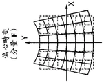
Here, a description is given as to what the mask means in an asymmetric shape. In the case where the reticle 9 is a usual single-layer reticle, not a multi-layer reticle, as shown in, for example, fig. 3A and 3B, the illumination area 90 of the reticle 9 arranged on the object plane of the projection optical system is a symmetrical shape with respect to the optical axis of the projection optical system. Here, "symmetrical" means that the center of mass of the illumination area is substantially the same as the optical axis of the projection optical system. In fig. 3A and 3B, an intersection point between the mask plane and the optical axis of the projection optical system is the origin. The solid line represents the outline of the reticle 9 and the dotted line represents the illumination area 90. Fig. 3A shows the case of the step-and-repeat (stepper) method, and fig. 3B shows the case of the step-and-scan (scanner) method. In both cases, the left and right ends of the illumination area are equidistant from the origin, the top and bottom ends of the illumination area are equidistant from the origin, and it can be seen that this forms a symmetrical shape. Note that with the step-and-scan method, during exposure, the reticle is moved along the Y-axis, while the illumination area is fixed with respect to the projection optical system. In other words, the symmetry of the illumination area is maintained for the projection optics, but not with respect to the reticle.
Meanwhile, in the case where exposure is performed by using a multilayer reticle, one region of the plurality of layer regions shown in fig. 2A to 2C becomes illuminated. Therefore, the centroid of the illumination area (i.e., the area of the layer) is different from the optical axis of the projection optical system, and the light beam passing through the projection optical system has an offset, rather than being symmetrical. In this specification, this state is discussed with "the mask is illuminated in an asymmetric shape".
Here, a description will be given about the asymmetric aberration. As described below, the asymmetric aberration includes at least one of an axis deviation, an eccentric distortion, a one-side defocus, an on-axis coma aberration, or a one-side defocus astigmatic aberration. Fig. 4A-4G are diagrams for describing various classifications of image shift errors. Distortion of an image in an image plane (image shift in the x-axis direction and the y-axis direction) is illustrated in fig. 4A to 4G, in which the origin is assumed as an intersection between the optical axis of the projection optical system and the image plane of the projection optical system, and the x-axis and the y-axis are within the image plane. The dashed grid indicates one shot in the case of an ideal projection, and the solid grid indicates one shot in the case of a projection with distortion. Magnification errors in fig. 4A, symmetric third-order distortion in fig. 4B, vertical/horizontal magnification factor errors (direction of 0 °) in fig. 4C, vertical/horizontal magnification factor errors (direction of 45 °) in fig. 4D, and the like are classified as symmetric errors. These have the property of rotational symmetry. For example, in the magnification error in fig. 4A and the symmetric third-order distortion in fig. 4B, there are four angles at which the grids self-overlap in one rotation around the origin, that is, there is four-fold symmetry. In addition, the vertical/horizontal magnification factor error (direction of 0 °) in fig. 4C and the vertical/horizontal magnification factor error (direction of 45 °) in fig. 4D have two-fold symmetry. Such aberrations having rotational symmetry are referred to as "symmetric aberrations".
On the other hand, in fig. 4A to 4G, the axis deviation in fig. 4E, the eccentric distortion (component E) in fig. 4F, and the eccentric distortion (component F) in fig. 4G are classified as asymmetric errors. These have no rotational symmetry. Such aberrations without rotational symmetry are referred to as "asymmetric aberrations". Note that the eccentric distortion of fig. 4F (component E) and the eccentric distortion of fig. 4G (component F) exemplify the eccentric distortion oriented in the y direction, but in fact, various orientations of the eccentric distortion may occur. The shaft offset may be similarly displaced in any direction. Also in such a case, the asymmetry is preserved. Note that higher order image shift components (symmetric and asymmetric) may be considered in addition to those illustrated here.
Fig. 5A to 5E are views for describing various classifications of focus errors. A focus error (image shift in the z-axis direction) in the image plane is illustrated in fig. 5A to 5E, and in fig. 5A to 5E, the origin is assumed to be the intersection between the optical axis of the projection optical system and the image plane, and the z-axis is parallel to the optical axis, and the x-axis and the y-axis are parallel to the image plane. The dashed grid indicates one shot in the case of ideal projection, and the solid grid indicates one shot in the case of focus error. Note that when there are two solid line grids, they illustrate two things: one is a plane (hface) constructed by connecting best focus points with respect to the horizontal pattern. The other is a plane (vefield) constructed by connecting best focus with respect to a vertical pattern (orthogonal pattern). A phenomenon in which the H image plane and the V image plane are deviated occurs if there is astigmatic aberration or the like, and the view illustrates such a case. Errors classified as symmetric are focus shift in fig. 5A, on-axis astigmatic aberration in fig. 5B, and field curvature in fig. 5C. These symmetric components have a characteristic of rotational symmetry similar to the case of image shift. Thus, there is at least one angle at which the aberration shape when rotated about the optical axis is aligned with the aberration shape before rotation. Meanwhile, errors classified as asymmetric are one-side defocus in fig. 5D and one-side defocus astigmatic aberration in fig. 5E. These have no rotational symmetry.
In addition, fig. 6A-6B illustrate the classification of coma aberration. Fig. 6A to 6B illustrate the magnitude and direction of coma aberration in the image plane with vectors, where the origin is assumed as the intersection between the optical axis of the projection optical system and the image plane, and the x-axis and the y-axis are parallel to the image plane. The error classified as symmetrical is third-order coma aberration in fig. 6A. Coma appears isotropically in proportion to the distance from the origin, and has a symmetrical shape. On the other hand, the error classified as asymmetric is central coma in fig. 6B. This has no rotational symmetry because coma of the same size and the same direction occurs uniformly in the screen. Note that fig. 6B illustrates the central coma oriented in one direction, and the coma may occur in virtually any direction.
The above is a description of representative symmetric aberrations and asymmetric aberrations. Here, distortion, focus error, astigmatism aberration, and coma aberration and other aberration components can be regarded as asymmetric components in the same manner. For example, each component of the wavefront aberration expressed by a Zernike polynomial expansion may be regarded as a component that is asymmetrically distributed in the image plane.
The inventors found that, if exposure is performed using a multilayer reticle, as described above, an aberration of an asymmetric component occurs as an exposure aberration. Fig. 7A to 7C illustrate exposure aberrations obtained by simulation that occur if exposure is performed using a multi-layer reticle. Fig. 7A illustrates the maximum exposure area 110 and the area 101 actually used for exposure in the projection optical system. Fig. 7B illustrates the image shift (distortion) occurring at this time. In addition, fig. 7C illustrates a focus error generated at this time. In all of these, it can be seen that errors occur intensively in the portion for exposure and have an asymmetric shape when the entire maximum exposure area is considered. It is difficult to express such asymmetric aberrations with a combination of conventional symmetric aberrations such as magnification change, symmetric third-order distortion, vertical/horizontal magnification factor error, focus shift, and field curvature. Therefore, in such a system based on symmetric aberrations, it is difficult to predict the amount of asymmetric exposure aberration that will occur or to perform correction thereof.
Note that in japanese patent No.5406437, since the exposure aberration coefficient is held for each image height, it can be said that there is a possibility that such an asymmetric image difference component can be handled. However, since it is necessary to hold a coefficient (parameter) for each image height, there is a problem that the number of parameters to be determined is large, and the number of experiments to be performed to obtain the parameters is large and time-consuming. In contrast to this, the present embodiment makes it possible to correct asymmetric exposure aberration that occurs when exposure is performed on an asymmetric exposure area with a multilayer reticle by a simple method.
Fig. 8 is a flowchart of a method for evaluating exposure aberration in the embodiment. The main controller 3 obtains the prediction coefficient for the asymmetric aberration in step S1. Next, a description will be given of specific details regarding step S1.
In step S1, a prediction coefficient for the asymmetric aberration is obtained by performing an experiment in advance using the exposure apparatus 100 before device manufacturing. If the exposure devices are of the same model, the standard prediction coefficients calculated using one device may be applied unchanged to the other device. Note that, since there are cases where the prediction coefficients are slightly different depending on individual differences or the like between devices, in the case where a prediction coefficient with high accuracy is required, the prediction coefficient may be recalculated by performing an experiment using each device.
The experiment for obtaining the prediction coefficient may be performed at the time of an assembly/adjustment step in a factory, or may be performed at the time of installation of the apparatus. Alternatively, the experiment may additionally be performed whenever there is an opportunity to use a multi-layer reticle. In the case where a multi-layer reticle to be used is identified, a prediction coefficient with higher accuracy can be obtained by obtaining a prediction coefficient using the reticle.
Hereinafter, a detailed description is given about a method for obtaining a prediction coefficient for an asymmetric aberration. First, in order to obtain a prediction coefficient for asymmetric aberration, the field stop 5 is set to a local arrangement so that only a part of the maximum exposure area is used similarly to when a multilayer reticle is used. Next, a reticle for testing is set in the exposure apparatus 100. The reticle used for the test is a reticle in which marks required for measuring a focus error and an image shift error are arranged in a sufficient number in an exposure area. For example, the marks are arranged in a grid pattern on a reticle for testing. Note that an actual multilayer reticle used for manufacturing a semiconductor device may be used as long as marks necessary for measuring a focus error or an image shift error are arranged thereon. Next, under the exposure condition, a focus error and an image shift error are measured in each of a plurality of exposure processes. For example, exposure is performed on a plurality of (e.g., from several to several hundreds) sample substrates, and a focus error and an image shift error are measured at a plurality of measurement points in each press shot of these sample substrates. Note that, since the exposure aberration has a property that it changes rapidly in the initial period of the start of exposure and it gradually saturates, the measurement can be performed by extracting some but not all of the sample substrates exposed after reaching the saturation phase. Further, by using the property of exposure aberration as described above, exposure may be sequentially performed so that the substrate is exposed mixedly in the dummy light-exposure as appropriate.
The main controller 3 obtains timing data for the symmetric aberration and the asymmetric aberration based on the results of the above measurements. Specifically, the main controller 3 decomposes the measurement results of the focus error and the image shift error obtained by the measurement at each measurement point using a method such as the least square method. In case of focus errors, a decomposition by terms is performed, which terms in addition to symmetric aberrations also comprise components of asymmetric aberrations such as, for example: focal shift, on-axis astigmatism, field curvature, one-sided defocus, and one-sided defocus astigmatic aberration. Furthermore, in case of image shift errors, a decomposition by terms is performed, said terms comprising, in addition to symmetric aberrations, components of asymmetric aberrations such as, for example: magnification error, symmetric third-order distortion, axial deviation, eccentric distortion, and the like. In this way, the timing fluctuation data for each aberration component is obtained.
The main controller 3 fits the model expression (prediction formula) to the thus obtained time-series fluctuation data for each aberration component, and finally obtains a prediction coefficient. For example, the following expression may be used as a model expression for fitting.


Here, F denotes the amount of change in the symmetric aberration of interest, G denotes the amount of change in the asymmetric aberration of interest, t denotes time, τ 1 、τ 2 、ν 1 V and v 2 Denotes the time constant, A 1 、A 2 、B 1 And B 2 Representing the amplitude. In such a case, 4 parameters A 1 、A 2 、τ 1 And τ 2 Called the prediction coefficient for symmetric aberrations (first prediction coefficient), 4 parameters B 1 、B 2 、ν 1 V and v 2 Referred to as the prediction coefficient for the asymmetric aberration (second prediction coefficient). Note that, a feature is that, in addition to the first prediction formula, the second prediction formula is newly added, the first prediction formula being a prediction formula for symmetric aberration, the second prediction formula being a prediction formula for asymmetric aberration. Conventionally, such a prediction formula for the asymmetric aberration is not considered.
Both the time constant and the coefficient are obtained by fitting. Alternatively, the configuration may be such that the time constant is fixed and only the coefficients are obtained using a fit if the time constant is known in advance. Note that A 1 、A 2 、B 1 And B 2 Is a function of the amount of energy per unit time (unit: W) applied to the projection optical system. In a simple model, A 1 、A 2 、B 1 And B 2 Proportional to the amount of energy per unit time applied to the projection optical system. In such a case, a can be made with the amount of energy per unit time applied to the projection optical system 1 、A 2 、B 1 And B 2 And (6) standardizing. Thus, a prediction of aberration during actual device fabrication can be calculated by multiplying the above equation by the amount of energy during device fabrication (e.g., every 1W). Note that, since both the symmetric aberration component and the asymmetric aberration component are used for component decomposition, prediction coefficients for both the symmetric aberration component and the asymmetric aberration component are obtained here. In the case where the aberration prediction is performed using the prediction coefficient for the asymmetric aberration component, it is always necessary to predict the symmetric aberration component using the prediction coefficient for the symmetric component calculated in set therewith. Therefore, these coefficients are stored in association in the exposure apparatus, and they are always used in sets.
Through the above processing, a prediction coefficient for symmetric aberration and a prediction coefficient for asymmetric aberration can be obtained. The obtained prediction coefficients are stored in the memory 32 of the exposure apparatus 100. Note that various region shapes can be considered for illumination regions where a multi-layer reticle is envisioned. As shown in fig. 2A-2C, this is because various patterns can be considered for the layer division method of the multilayer reticle. A plurality of prediction coefficients corresponding to various illumination region patterns can be obtained, all of which can be stored in the exposure apparatus. Further, since exposure aberration may vary depending on exposure conditions (such as NA or effective light source), it is more effective to save prediction coefficients obtained by varying these conditions in order to improve accuracy.
Next, in step S2, the main controller 3 obtains information of the shape of the illumination area on the mask surface. The control of the exposure apparatus 100 is performed by a user through a console or online setting of jobs and parameters in the exposure apparatus. The upper, lower, left and right blade position information on the field stop 5 (masking blade) is also one such parameter. Therefore, when the user inputs the setting value for the masking blade to the exposure device 100, the shape of the illumination area is set in the exposure device 100, whereby the exposure device 100 obtains information of the shape of the illumination area. Alternatively, the exposure apparatus 100 may have a file called "recipe" that describes the entire set of parameters of the exposure conditions. The user may save various parameters of the exposure conditions as a recipe in the exposure apparatus 100 in advance, and then the recipe may be called as appropriate to collectively set the parameters when performing the actual exposure. The setting value of the masking blade is also information saved in the recipe, and the setting value of the masking blade is set as the state of the exposure apparatus 100 by the user who called the recipe. In other words, when the user calls the recipe, the shape of the illumination area is set in the exposure apparatus 100, whereby the exposure apparatus 100 obtains information of the shape of the illumination area.
Next, the main controller 3 determines in step S3 whether the shape of the illumination area is symmetrical or asymmetrical. This is performed as follows. For example, the main controller 3 determines whether the shape of the illumination area is symmetrical or asymmetrical based on the information obtained in step S2 using calculation. For example, in the case where a condition that the centroid of the exposure region is sufficiently close to the optical axis of the projection optical system is satisfied, it can be determined that the shape of the illumination region is symmetrical. Alternatively, in the case where the condition that the top edge and the bottom edge and the left edge and the right edge of the masking blade are substantially equidistant from the optical axis of the projection optical system, respectively, is satisfied, it may be determined that the shape of the illumination area is symmetrical. Further, the user can determine whether the shape of the illumination area is symmetrical or asymmetrical, and input the result to the exposure apparatus 100. Alternatively, the user may input the shape of the "effective" illumination area to the exposure apparatus 100. This is because the reticle may be provided with a light-shielding tape, and when the width of the light-shielding tape is large, the illumination area defined by the masking blade may not necessarily coincide with the area actually exposed. In such a case, the user may manually input information to the exposure device. Further, in the case where the reticle being used is a multilayer reticle in which patterns of different layers are formed in a plurality of regions, respectively, it can be determined that the shape of the illumination region is asymmetric.
In steps S4 and S5, the aberration of the projection optical system is evaluated using at least one of a prediction coefficient for symmetric aberration (first prediction coefficient) and a prediction coefficient for asymmetric aberration (second prediction coefficient). Specifically, in the case where it is determined that the shape of the illumination area is symmetric, the main controller 3 evaluates the exposure aberration using only the prediction coefficients for the symmetric aberration in step S4. This will be described in detail below. In the case where the shape of the illumination area is determined to be symmetrical, the main controller 3 reads out the prediction coefficients for the symmetrical aberration from the memory 32. In some cases, a plurality of prediction coefficients obtained under different conditions related to NA, effective light source shape, screen size, and the like are stored in the memory 32. In this case, the main controller 3 may interpolate a plurality of prediction coefficients for different conditions based on the NA, effective light source, and masking blade position information (screen size information) recorded in the recipe to generate and then use new prediction coefficients. The prediction coefficients used in the recipe are determined by such processing. Note that, typically, the prediction coefficient for the symmetric aberration is obtained in the exposure apparatus mounting/adjusting step or the mounting step, unlike the prediction coefficient for the asymmetric aberration. Therefore, when exposure is started, the amount of aberration is calculated and predicted from the energy per unit time and the elapsed time applied in the projection optical system according to the model expression.
In the case where the shape of the illumination area is determined to be asymmetrical, the main controller 3 evaluates the exposure aberration using the prediction coefficient for the asymmetrical aberration and the prediction coefficient for the symmetrical aberration in step S5. This will be described in detail below. In the case where the shape of the illumination area is determined to be asymmetric, the main controller 3 reads the prediction coefficient for the asymmetric aberration and the prediction coefficient for the symmetric aberration as a set therewith from the memory 32. In the case where a plurality of asymmetric prediction coefficients obtained under different conditions are stored in the memory 32, a configuration may be adopted in which the prediction coefficients obtained under the most similar conditions are read based on NA, an effective light source, and position information on the masking blades (or shape information of an effective illumination area input by a user). Alternatively, a new prediction coefficient generated by interpolating a plurality of prediction coefficients whose conditions are different may be used. The prediction coefficients used in the recipe are determined by such processing. Moreover, the determined prediction coefficients are associated with the recipe. Then, when exposure is started, the amount of aberration is calculated and predicted (estimated) from the energy per unit time and the elapsed time applied in the projection optical system according to the model expression.
As described above, after evaluating the amount of aberration, the main controller 3 performs exposure while adjusting the exposure device based on the evaluation result so that the predicted amount of aberration is corrected. The symmetrical aberration component can be corrected with a correction system conventionally provided in an exposure apparatus. For example, the symmetric third-order distortion of the magnification error or the image shift error can be corrected by moving some of the lenses including the projection optical system parallel to the optical axis. Also, the vertical/horizontal magnification factor error of the image shift error can be corrected by constructing an Alvarez optical element in the projection optical system. Also, the focus shift of the focus error can be corrected by moving the substrate stage. For example, field curvature may be corrected by moving some of the lenses including the projection optical system parallel to the optical axis.
Furthermore, the asymmetric aberration can be corrected by changing the exposure apparatus parameters. For example, the axis deviation may be corrected by moving the substrate stage. Also, the decentering distortion (E, F component) can be corrected by slightly rotating some of the lenses including the projection optical system with an axis orthogonal to the optical axis as a rotation axis or by moving the lenses orthogonal to the optical axis. Also, one-side defocus can be corrected by tilting the substrate stage. Also, similarly to the decentering distortion, one-side defocusing astigmatic aberration and central coma can be corrected by slightly rotating some of the lenses including the projection optical system with an axis orthogonal to the optical axis as a rotation axis or by moving the lenses orthogonal to the optical axis. In this way, with the present embodiment, it is possible to correct not only symmetric aberration as conventionally done, but also asymmetric aberration. This is a feature not found in conventional methods. In other words, with the present embodiment, prediction and correction of exposure aberration are performed using the asymmetric image difference component in which the correction method exists. In this way, the prediction and subsequent correction can be smoothly connected.
In contrast, with the method in japanese patent No.5406437, since aberration prediction is performed for each image height, it is not immediately known whether it is a correctable component that can be predicted. Further, calculating the amount of movement of the correction system from the predicted aberration requires complicated calculation. Also, in the method of japanese patent No.5406437, since the prediction coefficient is held for each image height, the calculation of the prediction coefficient is more susceptible to the influence of measurement errors, and there is a corresponding possibility that the prediction accuracy will be degraded. Meanwhile, with the method of the present embodiment, the prediction coefficient is held after having been converted into the aberration component, rather than being held for each image height. Since processing for fitting between image heights is included, robustness against error is provided, and improvement in accuracy can be expected.
As described above, by switching the coefficients for prediction of exposure aberration depending on whether the illumination area is symmetrical or asymmetrical with respect to the optical axis of the projection optical system, aberration evaluation and correction more accurate than conventional can be easily performed. Therefore, improvement in accuracy and improvement in yield of the semiconductor device can be facilitated.
< second embodiment >
A description is given below about the exposure method in the second embodiment. Fig. 9 illustrates a reticle 9 as a multilayer reticle used in the present embodiment. Around each of the plurality of areas 91 and 92 used in exposure, a plurality of marks M for measuring focus/image shift are provided. The present embodiment is the same as the first embodiment in that it evaluates and corrects the asymmetrical exposure aberration when using a multilayer reticle. However, the present embodiment differs from the first embodiment in that the main controller 3 measures the asymmetric aberration between exposure sequences and feeds this back into the asymmetric aberration prediction coefficients.
For example, it is conceivable to arrange horizontal and vertical transmission line/space patterns as the marks M for measurement. A transmission window of a similar line/space pattern shape and an underlying light amount sensor are arranged at a specific position different from the position of the substrate on the substrate stage. When the mark M for measurement is illuminated with illumination light, an aerial image of a line/space pattern is formed on an image plane near the substrate stage surface via a projection optical system. The aerial image is measured through the transmission window and the underlying light sensor. The amount of light is measured while displacing the substrate stage surface in the defocus direction and the lateral direction, and the amount of shift in the defocus direction and the amount of shift in the lateral direction when the amount of light becomes maximum are the optimum focus and the optimum displacement point, respectively.
Such marks are provided, and for example, the marks M at four points of the periphery of the layer being exposed are measured at the timing at which the substrate is switched (measurement of the focus error and the image shift error). Then, component decomposition into a symmetric aberration component and an asymmetric aberration component by a least square method or the like is performed based on information of the focus error and the image shift error of the four points. By doing so, it is possible to know the amount of aberration that actually occurs. Whether prediction can be performed with high accuracy can be confirmed by comparing with the predicted value of the aberration calculated from the prediction coefficient. Therefore, it is possible to improve the prediction accuracy by feeding back the difference between the prediction and the amount of aberration actually occurring into the prediction coefficient.
For example, a focus error and an image shift error are measured between exposure sequences, actual symmetric aberration and asymmetric aberration data are obtained based on the measurement results, and the first prediction coefficient and the second prediction coefficient are corrected based on the obtained data. Therefore, improvement in the accuracy of the prediction coefficient can be achieved.
< example of method for producing article >
For example, the method of manufacturing an article according to an embodiment of the present invention is suitable for manufacturing an article such as an element having a microstructure or a microdevice (such as a semiconductor device). The method of manufacturing an article according to this embodiment includes a step of forming a latent image pattern on a photoresist applied to a substrate (a step of exposing the substrate) using the above-described exposure device, and a step of developing the substrate having the latent image pattern formed in the above step. The method of manufacture also includes other known steps (e.g., oxidation, deposition, vapor deposition, doping, planarization, etching, resist removal, dicing, bonding, and packaging). The method of manufacturing an article of the present embodiment has an advantage over conventional methods in at least one of the performance, quality, yield, and manufacturing cost of the article.
OTHER EMBODIMENTS
Embodiments of the invention may also be implemented by a computer of a system or apparatus that reads and executes computer-executable instructions (e.g., one or more programs) recorded on a storage medium (also may be more fully referred to as a "non-transitory computer-readable storage medium") to perform the functions of one or more of the above-described embodiments and/or include one or more circuits (e.g., an Application Specific Integrated Circuit (ASIC)) for performing the functions of one or more of the above-described embodiments, and embodiments of the invention may also be implemented by a computer of a system or apparatusThe machine is implemented by, for example, a method performed by reading out and executing computer-executable instructions from a storage medium to perform the functions of one or more of the above-described embodiments and/or to control one or more circuits to perform the functions of one or more of the above-described embodiments. The computer may include one or more processors (e.g., a Central Processing Unit (CPU), a Micro Processing Unit (MPU)) and may include a separate computer or a network of separate processors to read out and execute computer-executable instructions. The computer-executable instructions may be provided to the computer, for example, from a network or a storage medium. The storage medium may include, for example, one or more of the following: hard disk, Random Access Memory (RAM), read-only memory (ROM), storage for distributed computing systems, optical disk such as Compact Disk (CD), Digital Versatile Disk (DVD), or blu-ray disk (BD) TM ) Flash memory devices, memory cards, and the like.
OTHER EMBODIMENTS
The embodiments of the present invention can also be realized by a method in which software (programs) that perform the functions of the above-described embodiments are supplied to a system or an apparatus through a network or various storage media, and a computer or a Central Processing Unit (CPU), a Micro Processing Unit (MPU) of the system or the apparatus reads out and executes the methods of the programs.
While the present invention has been described with reference to exemplary embodiments, it is to be understood that the invention is not limited to the disclosed exemplary embodiments. The scope of the following claims is to be accorded the broadest interpretation so as to encompass all such modifications and equivalent structures and functions.
Claims (9)
1. An evaluation method for evaluating aberration of a projection optical system in an exposure apparatus, the method comprising:
obtaining a first prediction coefficient which is a prediction coefficient of a first prediction formula which is a prediction formula for an aberration that is symmetrical with respect to an optical axis of the projection optical system, and obtaining a second prediction coefficient which is a prediction coefficient of a second prediction formula which is a prediction formula for an aberration that is asymmetrical with respect to the optical axis of the projection optical system;
determining whether or not a center of a rectangular illumination region in an object plane of a projection optical system in which a mask is arranged coincides with an optical axis in a case where a shape of the illumination region is a rectangle; and
estimating aberrations of the projection optical system using at least one of the first prediction coefficient and the second prediction coefficient, wherein the estimating step includes:
in a case where the determining step determines that the center of the rectangular illumination area in the object plane coincides with the optical axis, evaluating aberration of the projection optical system using the first prediction coefficient; and
in a case where the determination step determines that the center of the rectangular illumination area in the object plane does not coincide with the optical axis, the aberration of the projection optical system is evaluated using the first prediction coefficient and the second prediction coefficient.
2. The evaluation method of claim 1, wherein the obtaining step comprises:
measuring a focus error and an image shift error in each of a plurality of exposure processes;
obtaining time series data of the symmetric aberration and the asymmetric aberration based on the result of the measurement; and
the first prediction coefficient is obtained by fitting the first prediction formula to the time series data of the symmetric aberration, and the second prediction coefficient is obtained by fitting the second prediction formula to the time series data of the asymmetric aberration.
3. The evaluation method according to claim 2, wherein the plurality of exposure processes include a plurality of exposure processes whose illumination areas are respectively different, wherein the illumination areas are a plurality of rectangular partial areas having different centers that are not coincident with the optical axis in the object plane.
4. The evaluation method according to claim 1, wherein the determining step determines that the center of the illumination area coincides with the optical axis in a case where the center of mass of the exposure area is close to the optical axis.
5. The evaluation method according to claim 1, wherein the determining step determines that the center of the illumination area does not coincide with the optical axis in a case where the mask is a multi-layer reticle having different layer patterns formed in a plurality of areas, respectively.
6. The evaluation method of claim 1, further comprising:
the focus error and the image shift error are measured between exposure sequences, data of symmetric aberration and asymmetric aberration are obtained based on the results of the measurement, and the first prediction coefficient and the second prediction coefficient are corrected based on the obtained data.
7. The evaluation method according to claim 1, wherein the asymmetric aberration includes at least one of an axis deviation, an eccentric distortion, a one-side defocus, an on-axis coma aberration, and a one-side defocus astigmatic aberration.
8. An exposure method performed by an exposure apparatus that projects a pattern formed on a mask onto a substrate via a projection optical system and exposes the substrate, the method comprising:
evaluating aberrations of a projection optical system by using the evaluation method according to claim 1;
adjusting an exposure device based on a result of the evaluation; and
the substrate is exposed using the adjusted exposure apparatus.
9. A method for manufacturing an article, comprising:
exposing the substrate according to the exposure method of claim 8; and
the exposed substrate is developed and then,
wherein the article is manufactured from the developed substrate.
Applications Claiming Priority (2)
| Application Number | Priority Date | Filing Date | Title |
|---|---|---|---|
| JP2018-100863 | 2018-05-25 | ||
| JP2018100863A JP7054365B2 (en) | 2018-05-25 | 2018-05-25 | Evaluation method, exposure method, and article manufacturing method |
Publications (2)
| Publication Number | Publication Date |
|---|---|
| CN110531587A CN110531587A (en) | 2019-12-03 |
| CN110531587B true CN110531587B (en) | 2022-09-27 |
Family
ID=68614496
Family Applications (1)
| Application Number | Title | Priority Date | Filing Date |
|---|---|---|---|
| CN201910420978.6A Active CN110531587B (en) | 2018-05-25 | 2019-05-21 | Evaluation method, exposure method, and method for manufacturing article |
Country Status (3)
| Country | Link |
|---|---|
| US (1) | US10545413B2 (en) |
| JP (1) | JP7054365B2 (en) |
| CN (1) | CN110531587B (en) |
Families Citing this family (2)
| Publication number | Priority date | Publication date | Assignee | Title |
|---|---|---|---|---|
| US11893668B2 (en) | 2021-03-31 | 2024-02-06 | Leica Camera Ag | Imaging system and method for generating a final digital image via applying a profile to image information |
| WO2023138892A1 (en) * | 2022-01-24 | 2023-07-27 | Asml Netherlands B.V. | Method and apparatus for illumination adjustment |
Citations (2)
| Publication number | Priority date | Publication date | Assignee | Title |
|---|---|---|---|---|
| JP2006073584A (en) * | 2004-08-31 | 2006-03-16 | Nikon Corp | Exposure apparatus and exposure method, and device manufacturing method |
| CN107065447A (en) * | 2016-02-10 | 2017-08-18 | 台湾积体电路制造股份有限公司 | The method configured for the asymmetric pupil provided for extreme ultraviolet photoetching process |
Family Cites Families (6)
| Publication number | Priority date | Publication date | Assignee | Title |
|---|---|---|---|---|
| JP2503451B2 (en) * | 1985-12-26 | 1996-06-05 | 株式会社ニコン | Projection exposure method and apparatus |
| TW500987B (en) | 2000-06-14 | 2002-09-01 | Asm Lithography Bv | Method of operating an optical imaging system, lithographic projection apparatus, device manufacturing method, and device manufactured thereby |
| JP5406437B2 (en) | 2007-06-22 | 2014-02-05 | キヤノン株式会社 | Exposure apparatus and device manufacturing method |
| JP4944690B2 (en) * | 2007-07-09 | 2012-06-06 | キヤノン株式会社 | Method for adjusting position detection apparatus, position detection apparatus, exposure apparatus, and device manufacturing method |
| NL2008310A (en) | 2011-04-05 | 2012-10-08 | Asml Netherlands Bv | Lithographic method and assembly. |
| JP6381188B2 (en) | 2013-08-13 | 2018-08-29 | キヤノン株式会社 | Exposure apparatus and device manufacturing method |
-
2018
- 2018-05-25 JP JP2018100863A patent/JP7054365B2/en active Active
-
2019
- 2019-05-15 US US16/412,524 patent/US10545413B2/en active Active
- 2019-05-21 CN CN201910420978.6A patent/CN110531587B/en active Active
Patent Citations (2)
| Publication number | Priority date | Publication date | Assignee | Title |
|---|---|---|---|---|
| JP2006073584A (en) * | 2004-08-31 | 2006-03-16 | Nikon Corp | Exposure apparatus and exposure method, and device manufacturing method |
| CN107065447A (en) * | 2016-02-10 | 2017-08-18 | 台湾积体电路制造股份有限公司 | The method configured for the asymmetric pupil provided for extreme ultraviolet photoetching process |
Also Published As
| Publication number | Publication date |
|---|---|
| CN110531587A (en) | 2019-12-03 |
| JP7054365B2 (en) | 2022-04-13 |
| US10545413B2 (en) | 2020-01-28 |
| US20190361355A1 (en) | 2019-11-28 |
| JP2019204058A (en) | 2019-11-28 |
Similar Documents
| Publication | Publication Date | Title |
|---|---|---|
| JP4352458B2 (en) | Projection optical system adjustment method, prediction method, evaluation method, adjustment method, exposure method and exposure apparatus, exposure apparatus manufacturing method, program, and device manufacturing method | |
| KR100879306B1 (en) | Measurement method and apparatus, exposure apparatus | |
| US6278514B1 (en) | Exposure apparatus | |
| KR102002666B1 (en) | Exposure apparatus, exposure method, and device manufacturing method | |
| US20090170042A1 (en) | Exposure apparatus and device manufacturing method | |
| WO2011061928A1 (en) | Optical characteristic measurement method, exposure method and device manufacturing method | |
| JP2002071514A (en) | Inspection apparatus, exposure apparatus provided with the inspection apparatus and production method of micro device | |
| CN110531587B (en) | Evaluation method, exposure method, and method for manufacturing article | |
| JP4568340B2 (en) | Manufacturing method of semiconductor device | |
| JP6917477B2 (en) | Lithography equipment and lithography method | |
| KR101530747B1 (en) | Exposure apparatus and device fabrication method | |
| KR101320240B1 (en) | Wavefront aberration measurement apparatus, exposure apparatus, and method of manufacturing device | |
| US10394134B2 (en) | Exposure method, exposure apparatus, and method of manufacturing article | |
| JP4416540B2 (en) | Aberration measurement method | |
| US20240126182A1 (en) | Exposure apparatus, control method of exposure apparatus, information processing apparatus, information processing method, and article manufacturing method | |
| JP2003178968A (en) | Method of measuring aberration and projection exposure system | |
| JP6448220B2 (en) | Exposure apparatus, exposure method, and device manufacturing method | |
| JP7378265B2 (en) | Exposure equipment, exposure method, and article manufacturing method | |
| KR20240051826A (en) | Exposure apparatus, control method of exposure apparatus, information processing apparatus, information processing method, and article manufacturing method | |
| JP2024057976A (en) | Exposure apparatus, exposure apparatus control method, information processing apparatus, information processing method, and article manufacturing method | |
| US20090213388A1 (en) | Measurement method and measurement reticle | |
| CN117950275A (en) | Exposure method, exposure apparatus, and method for manufacturing article | |
| JP2022185871A (en) | Exposure method, exposure device and article manufacturing method | |
| JP2007150354A (en) | Pattern predicting method and program | |
| JP2010133980A (en) | Inspection apparatus, exposure device having the same, and method of manufacturing micro device |
Legal Events
| Date | Code | Title | Description |
|---|---|---|---|
| PB01 | Publication | ||
| PB01 | Publication | ||
| SE01 | Entry into force of request for substantive examination | ||
| SE01 | Entry into force of request for substantive examination | ||
| GR01 | Patent grant | ||
| GR01 | Patent grant |