CN1103476C - Image forming appts. - Google Patents
Image forming appts. Download PDFInfo
- Publication number
- CN1103476C CN1103476C CN97190191A CN97190191A CN1103476C CN 1103476 C CN1103476 C CN 1103476C CN 97190191 A CN97190191 A CN 97190191A CN 97190191 A CN97190191 A CN 97190191A CN 1103476 C CN1103476 C CN 1103476C
- Authority
- CN
- China
- Prior art keywords
- pixel data
- address
- cache memory
- data item
- data
- Prior art date
- Legal status (The legal status is an assumption and is not a legal conclusion. Google has not performed a legal analysis and makes no representation as to the accuracy of the status listed.)
- Expired - Lifetime
Links
Images


Classifications
-
- G—PHYSICS
- G06—COMPUTING; CALCULATING OR COUNTING
- G06T—IMAGE DATA PROCESSING OR GENERATION, IN GENERAL
- G06T1/00—General purpose image data processing
-
- G—PHYSICS
- G09—EDUCATION; CRYPTOGRAPHY; DISPLAY; ADVERTISING; SEALS
- G09G—ARRANGEMENTS OR CIRCUITS FOR CONTROL OF INDICATING DEVICES USING STATIC MEANS TO PRESENT VARIABLE INFORMATION
- G09G5/00—Control arrangements or circuits for visual indicators common to cathode-ray tube indicators and other visual indicators
- G09G5/36—Control arrangements or circuits for visual indicators common to cathode-ray tube indicators and other visual indicators characterised by the display of a graphic pattern, e.g. using an all-points-addressable [APA] memory
- G09G5/39—Control of the bit-mapped memory
- G09G5/393—Arrangements for updating the contents of the bit-mapped memory
-
- G—PHYSICS
- G06—COMPUTING; CALCULATING OR COUNTING
- G06T—IMAGE DATA PROCESSING OR GENERATION, IN GENERAL
- G06T1/00—General purpose image data processing
- G06T1/20—Processor architectures; Processor configuration, e.g. pipelining
-
- G—PHYSICS
- G06—COMPUTING; CALCULATING OR COUNTING
- G06T—IMAGE DATA PROCESSING OR GENERATION, IN GENERAL
- G06T1/00—General purpose image data processing
- G06T1/60—Memory management
-
- G—PHYSICS
- G09—EDUCATION; CRYPTOGRAPHY; DISPLAY; ADVERTISING; SEALS
- G09G—ARRANGEMENTS OR CIRCUITS FOR CONTROL OF INDICATING DEVICES USING STATIC MEANS TO PRESENT VARIABLE INFORMATION
- G09G5/00—Control arrangements or circuits for visual indicators common to cathode-ray tube indicators and other visual indicators
- G09G5/36—Control arrangements or circuits for visual indicators common to cathode-ray tube indicators and other visual indicators characterised by the display of a graphic pattern, e.g. using an all-points-addressable [APA] memory
-
- G—PHYSICS
- G09—EDUCATION; CRYPTOGRAPHY; DISPLAY; ADVERTISING; SEALS
- G09G—ARRANGEMENTS OR CIRCUITS FOR CONTROL OF INDICATING DEVICES USING STATIC MEANS TO PRESENT VARIABLE INFORMATION
- G09G2340/00—Aspects of display data processing
- G09G2340/10—Mixing of images, i.e. displayed pixel being the result of an operation, e.g. adding, on the corresponding input pixels
-
- G—PHYSICS
- G09—EDUCATION; CRYPTOGRAPHY; DISPLAY; ADVERTISING; SEALS
- G09G—ARRANGEMENTS OR CIRCUITS FOR CONTROL OF INDICATING DEVICES USING STATIC MEANS TO PRESENT VARIABLE INFORMATION
- G09G2360/00—Aspects of the architecture of display systems
- G09G2360/12—Frame memory handling
- G09G2360/121—Frame memory handling using a cache memory
Landscapes
- Engineering & Computer Science (AREA)
- Physics & Mathematics (AREA)
- General Physics & Mathematics (AREA)
- Theoretical Computer Science (AREA)
- Computer Hardware Design (AREA)
- Image Generation (AREA)
- Controls And Circuits For Display Device (AREA)
- Memory System Of A Hierarchy Structure (AREA)
- Image Input (AREA)
- Memory System (AREA)
- Digital Computer Display Output (AREA)
- Storing Facsimile Image Data (AREA)
Abstract
Data from a main part of a drawing engine 101 is sent to and transiently stored in a first-in-first-out (FIFO) memory 102 for storage transiently therein and is supplied via an operating device 103 to a fast cache memory 104 where data exchange is carried out with a frame buffer 105. A cache controller 106 controls the cache memory 104 for pre-reading the contents of the FIFO memory 102 and collectively reading/writing data of the same page in the frame buffer 105 which is accessible at a high speed. This enables fast accessing using an inexpensive frame buffer to improve the drawing speed.
Description
Technical field:
The present invention relates to image forming appts, particularly utilize the video generation device that uses in the video equipment of computing machine, for example graphic computer, effect machine or video game machine.
Background technology
In utilizing the equipment of computer graphical, for example video game machine, personal computer or graphic computer, in order to form the image that view data or formation outputed to and be presented at television receiver, warning receiver or cathode ray tube (CRT) display device, carry out geometric manipulations or imaging processing.Coordinate conversion is carried out in the geometric manipulations unit, shear or light source calculating, and the imaging processing unit will consider to form polygonal all color of pixel and Z value according to the color data on summit and the Z value of the expression degree of depth, and pixel data is write video memory.
In order to realize this processing, imaging processing particularly recited above adopts and draws treatment circuit or drawing engine, and drawing engine utilizes the method for the pixel that forms directly being write video memory usually.
And the render speed of image is subjected to by the influence of drawing engine to the video memory writing rate.Like this, image memory access speed is slow, and render speed just reduces.Therefore, if in order to increase render speed, use expensive high-speed memory as large capacity image memory, the cost of system can be crossed the highland and increase, and if use dynamic RAM (DRAM) at a low price, the render speed of system reduces.
Can imagine, the memory buffer of a corresponding DRAM page is provided between drawing engine and video memory, and only use and transmit the access images storer at a high speed in groups, yet, if drawing data appears in the sequence of cross-over connection margin edge in the memory buffer range of capacity, then cause low efficient.
In view of the above problems, the invention provides a kind of image forming appts, thereby, even use storer at a low price,, also can keep high render speed as DRAM.
Summary of the invention:
The invention provides a kind of image forming appts, comprising: drawing apparatus is used for generating the pixel data item (item) that each all comprises address and pixel data continuously according to image information; A temporary storage is used for storing the pixel data item that described drawing apparatus generates, and is used for exporting continuously described pixel data item; A cache memory; A frame memory is used for the storage pixel data; The speed buffering control device is used for the address according to the pixel data item of being exported, and wherein pixel data is write in the cache memory; And operating means, be used for before the described pixel data item of output the address of reading the pixel data item that is stored in the described temporary storage.Wherein, pixel data in the described operating means retrieval cache memory, have the value identical and satisfy the pixel data of specified requirements with the specified portions that detects its address with the specified portions of reading the address, and the visit frame memory caches to cache memory so that once will be arranged in the pixel data at the pixel data of reading the place, address and the place, address that is positioned at the pixel data that is detected.
According to image forming appts of the present invention, wherein work as the pixel data that is detected and satisfy described specified requirements when invalid, thereby the pixel data that will not be detected is retained in the cache memory.
According to image forming appts of the present invention, wherein, each of pixel data item all comprises an operational order; And described speed buffering control device carries out processings of Z impact damper, antialiasing processing, Screening Treatment, α-hybrid processing, translucent processing and the pixel permutatation at least one item in handling according to the operational order in the pixel data item of output to the pixel data item of output, and the pixel data after will handling writes in the cache memory.
The present invention also provides a kind of video game machine that comprises above-mentioned video generation device.
The present invention also provides a kind of method that is used in the video generation device, and described video generation device comprises: drawing apparatus is used for generating the pixel data item that each all comprises address and pixel data continuously according to image information; A temporary storage is used for storing the pixel data item that described drawing apparatus generates, and is used for exporting continuously the pixel data item of being stored; A cache memory; A frame memory is used for the storage pixel data, and described method comprises the following steps: according to the address in the pixel data item of being exported, and wherein pixel data is write in the cache memory; Before the described pixel data item of output, the address of reading the pixel data item that is stored in the described temporary storage; And the pixel data in the retrieval cache memory, have the value identical and satisfy the pixel data of specified requirements with the specified portions that detects its address with the specified portions of reading the address, and the visit frame memory caches to cache memory so that once will be arranged in the pixel data at the pixel data of reading the place, address and the place, address that is positioned at the pixel data that is detected.
According to image forming appts of the present invention, the view data that is formed by drafting treating apparatus such as drawing engine temporarily is stored in the storer, as the FIFO storer, one fast high-speed cache be arranged between FIFO storer and the frame buffer, the content of FIFO storer is read in advance by cache control device, with the read/write of control to cache memory.Therefore,, can realize zero access, draw efficient to improve through high-speed cache if storer at a low price is used as frame buffer as DRAM commonly used.At this moment, the data of the one page of collective's read and write efficiently frame buffer are to realize quick access.
Operating means between FIFO storer and high-speed cache is used to realize the Z buffered, and antialiasing is handled, various screening operations, and α-hybrid processing, translucent processing or pixel permutatation are handled.
Description of drawings:
Fig. 1 is the principle structure block diagram of one embodiment of the present of invention, and image forming appts wherein is used in the video game machine.
Fig. 2 is the block diagram of the structure of graphic process unit, and graphic process unit is according to the image processing apparatus in the image forming appts of the present invention.
The block diagram of Fig. 3 structure that is apparatus of the present invention between the frame buffer of the major part of drawing engine and image forming appts.
Fig. 4 has shown the example of data structure in the FIFO storer.
Fig. 5 has shown the example of data structure in Cache.
Fig. 6 is the operation when being provided with memory buffer between drawing engine and frame buffer.
Fig. 7 has shown the data structure in the common cache memory.
Fig. 8 has shown the principle structure block diagram when between the major part of drawing engine and frame buffer common cache memory being set.
Fig. 9 has shown the operational flowchart of structure shown in Figure 8.
Figure 10 has illustrated the drawing data string has been write operation in the frame buffer.
Figure 11 is a process flow diagram, and the read operation of by director cache the FIFO storer being carried out by the structure of Fig. 3 first time has been described.
Figure 12 is a process flow diagram, has illustrated by the structure of Fig. 3 to pass through the read/write operation of high speed unwinding controller to cache memory.
Figure 13 is the square circuit diagram of specific examples of the operating means of Fig. 3.
Figure 14 is the circuit diagram of specific examples of the operating means of Figure 13.
Figure 15 is the plan view of the video game machine of the embodiment of the invention.
Figure 16 is the rear view of video game machine.
Figure 17 is the side view of video game machine.
Figure 18 is the plan view that is loaded in the CD-ROM on the video game apparatus.
Embodiment:
With reference to the accompanying drawings, describe the preferred embodiments of the present invention below in detail.Fig. 1 illustrates the principle structure of video game machine according to the present invention as image forming appts.
The games that are stored in auxilary unit such as the CD are read and carried out to video game machine shown in Figure 1, carries out recreation with the instruction of sending according to the user.
Particularly, this video game machine has two class buses, i.e. main bus 1 and sub-bus 2, and main bus 1 and sub-bus 2 are interlinked through bus controllers 16.
Link on the main bus 1 by the CPU (central processing unit) of forming by microprocessor (CPU) 11, the primary memory of forming by random-access memory (ram) 12, active attitude memory access controller or main DMAC 13, mpeg decoder 14 and graphics processing unit or Graphics Processing Unit (GPU) 15, be connected with the auxiliary centre processing unit or the sub-CPU 21 that form by microprocessor on the sub-bus 2, the supplementary storage of forming by random-access memory (ram), auxiliary DYNAMIC MEMORY ACCESS controller or sub-DMAC 23, the for example ROM (read-only memory) of operating system (ROM) 24 wherein has program stored therein, sound processing unit (SPU) 25, communication controler or asynchronous transfer mode (ATM) 26, auxilary unit 27, input media 28 and CD-ROM drive 30.
GPU 15 is devices on the main bus 1, play imaging processor, GPU 15 analyzes the rendering order of the order packet form of sending from host CPU 11 or main DMAC 13, according to the Z value of designated depth with form polygonal all color of pixel values, in as the frame buffer 18 of video memory, realize writing the imaging processing of pixel data.
But MDEC 14 be one with the I/O hookup mechanism of host CPU parallel work-flow and on bus 1 as the device of image spreading engine.Orthogonal transformation is used in MDEC 14 decodings, as discrete cosine transform compression and image encoded data.Sub-CPU 21 is according to the device of the procedure operation on the quantum memory 22 on the sub-bus 2.
SPU 25 is the devices that play the Sound Processor Unit effect on the sub-bus 2.The voice command that SPU 25 response is sent as the order bag from sub-CPU 21 or sub-DMAC 23, according to the order bag from acoustic memory 29 sound source data of reading aloud, output sense data.
The input media that input media 28 is made up of some other equipment, as the control panel on sub-bus 2, man-machine interface, Genius mouse for example, image input or phonetic entry.
CD-ROM drive 30 is the data input devices on the sub-bus 2, is used for from CD-ROM copying application program and required data.
In the just described in the above video game machine, the geometric manipulations system carries out geometric manipulations, as coordinate transform, shears or light source calculating.For drawing three-dimensional figure, represent by elementary cell figure (polygon) as triangle or tetragonal combination and the rendering order of the three-dimensional model that defines with formula, and delivering to main bus 1 with the relevant rendering order of each polygon as the order bag, these functions are formed by host CPU on the main bus 1 11 and GTE 17.In addition, the imaging processing system is made up of GPU 15, and this imaging processing system works out each polygonal pixel data according to the rendering order in the geometric manipulations system, to write frame buffer 18, draws figure with image processing method in frame buffer 18.
Detailed structure with reference to GPU 15 shown in Figure 2, GPU 15 comprises the imaging processing linking the bag engine 31 on the main bus 1 and realize writing each the polygon pixel data in the frame buffer 18 by pretreater 32, also comprise drawing engine 33, it is according to the rendering order of delivering to bag engine 31 from the conduct order bag of host CPU 11 or main DMAC by main bus 1, read out in the pixel data of institute's drawing picture in the frame buffer 18, and the pixel data of being read is offered television receiver or monitor receiver (not shown) as vision signal through CRT controller 34.
Bag engine 31 produces an order bag, is transferred to the register (not shown) by main bus 1 from host CPU 11 or main DMAC 13.
Pretreater 32 forms polygon data according to the rendering order of giving bag engine 31 by the order bag, and realizes the pre-service of presetting.Cut apart as the polygon to polygon data that will illustrate in the back, produce various data simultaneously, each polygonal apex coordinate information required as drawing engine 33, as texture or MIP mapping texture address information, or as the control information of pixel decomposition usefulness.
Drawing engine 33 comprises N the polygon engine 3 3A1 that links respectively on the pretreater 32,33A2 ... 33AN; Link polygon engine 3 3A1 respectively, 33A2 ... the N on the 33AN grain engine 33B1,33B2 ... 33BN; Link grain engine 33B1,33B2 ... the first bus converter 33C of 33BN; Link M the pixel engine 33D1 of the first bus converter 33C, 33D2 ... 33DM; Link pixel engine 33D1,33D2 ... the 2nd bus converter 33E of 33DM; Link the texture cache 33F and the CLUT high-speed cache 33G that links on the texture cache 33F of the second bus converter 33E.
In drawing engine 33, N polygon engine 3 3A1,33A2 ... 33AN sequentially produces polygon according to the pre-service of 32 pairs of polygon datas of pretreater by rendering order, so that realize the Rendering Process that walks abreast from a polygon to another polygon.
N grain engine 33B1,33B2, ... 33BN is by polygon engine 3 3A1,33A2, ... on each polygon that 33AN produces, based on from texture cache 33F through the data texturing that color look-up table (CLUT) high-speed cache 33G provides, realize that concurrently texture or MIP mapping handles.
Pretreater 32 provides address information as appending to by N grain engine 33B1 in advance, 33B2 ... texture on the polygon that 33BN handles or MIP mapping texture are given texture cache 33F.According to the above address information, required data texturing is sent to frame buffer 18 from texture area, and the CLUT data that will relate to during texture is drawn are sent to the CLUT district of frame buffer 18 from CLUT high-speed cache 33G.
By N grain engine 33B1,33B2 ... the polygon data that 33BN handles by texture or MIP mapping, pass to M pixel engine 33D1 through the first bus converter 33C, 33D2 ... 33DM.
M pixel engine 33D1,33D2 ... 33DM carries out various image processing operations, and the Z impact damper is handled or antialiasing is handled as carrying out concurrently, to form M pixel data.
By M pixel engine 33D1,33D2 ... M the pixel data that 33DM forms is written in the frame buffer 18 through the second bus converter 33E.
The second bus converter 33E obtains pixel and decomposes control information from pretreater 32, the second bus converter 33E is according to above-mentioned control information, from M pixel engine 33D1,33D2, ... select L pixel data in M the pixel data that 33DM produces, carry out pixel resolution process function,, write M pixel data with M the memory address that meets as the polygonal shape in the frame buffer 18 of access unit.
Drawing engine 33 produces and writes each polygonal whole pixel data according to pretreater 32 pretreated polygon datas in frame buffer 18, with by rendering order, on frame buffer 18, draw the image by polygon combination definition.The pixel data of the image of frame buffer 18 is read out and offers television receiver or monitor receiver (not shown) by CRTC 34 as vision signal.
Fig. 3 has illustrated the n-lustrative structure between the major part of drawing engine 33 and frame buffer 18.
In Fig. 3, the major part 101 of drawing engine 33 is corresponding to pixel engine 33D1 shown in Figure 2,33D2, ... the top of the structure of 33DM, each pixel engine 33D1,33D2, ... 33DM comprises first in first out (FIFO) storer 102 as shown in Figure 3, operating means 103, high-speed cache 104 and speed buffering controller 106, the pixel data that major part 101 outputs of drawing engine will be drawn, and pixel data is delivered to FIFO storer 102, temporarily be stored in wherein, this FIFO storer 102 can be as the back be illustrated, the content of pre-memory read, and read in advance by 106 controls of speed buffering controller.
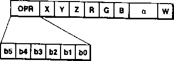
The order of structure shown in FIFO storer 102, being written among data or Fig. 4 as an example, wherein OPR represents operational code, X, Y and Z denotation coordination value, R, G and B and α represent color value, W represents to write the permission mark, operational code OPR is by forming to b5 as 6 b0, and its meta b0 indicates whether to have formed the α mixing with 1 or 0, and a position b2 indicates whether that with 1 or 0 the Z impact damper is used.Position b2 and b3 are illustrated respectively in the multiplication factor of vertical and horizontal, represent the factor 1 and 2 with 0 and 1 respectively.If b2 is 1, Y is 2 multiplication factor, draws 2 vertical pixels according to 2 vertical pixels.If b3 is 1, X is 2 multiplication factor, draws pixels across according to 2 pixels across.Position b5 and b4 are used for selecting screening or antialiasing.If position b5 and b4 are 00,01,10 or 11, then carry out directly respectively and draw antialiasing, the screening of the screening of Class1 and type 2.
The operating means 103 of Fig. 3 is made up of comparer that will illustrate later on or effector, and reads operation and the comparison that pixel goes to carry out the required Z value of pixel from FIFO storer 102.And operating means 103 is carried out and is write, and the Z impact damper is handled, and mixes translucent processing, antialiasing, various screenings and pixel permutatation operation.High-speed cache 104 utilizes storer such as common random access memory (DRAM) at a low price, carries out the block transfer with next stage frame buffer 105.
Fig. 5 has shown the data structure of cache memory, wherein Tag is distinguished or the territory by the mark (tag) that page address Page and column address Col form, DT is the data field, S and V are sign (flag) districts, whether cue mark and data are effective, and RC is the request count block, the count value of designation data request of access, frame buffer 105 is equivalent to the frame buffer 18 among Fig. 1 and 2, and this delegation calls with the delegation of the high-speed cache 104 that has 2 row or multirow memory span usually.Usually, the page address Page of mark zone and column address Col represent the high address of row address or column address or frame buffer 105 respectively.
Director cache 106 is a kind of control device, be used for controlling cache memory 104, director cache 106 sends the content that FIFO storer 102 is checked in instruction in advance, understand required data field, if enough spare regions are arranged in cache memory 104, director cache sends instruction, rearrange the data order that the data field occurs, and group address (for example DRAM) is with the same one page in the one frame buffer 105, director cache 106 also sends instruction, the data of director cache 104 are sent to frame buffer 105 jointly, so that does not cross on the border of the word boundary of DRAM or page or leaf, the number of times of result's visit and the time of visit will shorten, and the operation of director cache 106 will illustrate below.
Utilize above-mentioned image forming appts, the drafting efficient of drawing engine can be improved, and the Z impact damper, antialiasing, various screening operations, α mixes, and translucence is handled or the permutatation of pixel is handled and can be realized effectively.
Before top embodiment method was described in more detail, the relevant technologies and the reference example of pixel data write in explanation earlier in frame buffer by drawing engine.
When the direct access frame buffer of drawing engine, therefore the speed of drawing, need expensive high-speed large capacity memory by the decision of frame buffer access speed, if as frame buffer, draw speed and slowed down as the front is said with the DRAM of common low price.
Suppose between drawing engine and frame buffer, provide can the high speed block transfer memory buffer, for example, suppose capacity that memory buffer 107 has delegation corresponding to frame buffer 105, that is to say one page among Fig. 6, drawing data string L1, L2, L3 and L4 are one after the other drawn by drawing engine.In this case, drawing data string L1, L3 and drawing data string L2, L4 are plotted in respectively among the district 105a and 105b of frame buffer 105.
Drawing engine is write in buffer memory 107 before the drawing data string L1, and the data among the regional 105a of frame buffer 105 are read out, and just are loaded onto buffer memory 107 by block transfer.When drawing next drawing data string L2, the content of memory buffer 107 is written to regional 105a by block transfer, and the data of the regional 105b of frame buffer 105 are read (loadings) and arrived memory buffer 107.Then, drawing data string L2 is written to memory buffer 107, when drawing next drawing data string L3, the content of memory buffer 107 is written to the regional 105b of frame buffer 105, and the content of following regional 105a is read frame buffer 107 with en bloc transmission, and drawing data string L3 is written to followed by the position below the drawing data string L1, when drawing next drawing data string L4, drawing data string L1 in frame buffer 107, L3 is written among the regional 105a of frame buffer 105.Then, the content of regional 105b is written to frame buffer 107, and drawing data string L4 is written on the position below the drawing data string L2 and then.
In the structure of utilizing memory buffer 107, because the visit of frame buffer occurs continually, the effect of the high speed access of block transfer can not be manifested accidentally fully.
Suggestion is provided with the cache memory 108 of structure as shown in Figure 7, as shown in Figure 8 between the major part and frame buffer 105 of drawing engine 101.Cache memory 108 is by speed buffering controller 109 its reading and writing datas of control.Although the memory construction of Fig. 7 is substantially similar to Fig. 5, it is only with a V (effectively) sign, as common cache architecture.
(if adopting this cache memory 108) drawing data string L1, L2, the drawn engine 101 of L3 and L4 is drawn in succession, the data of the regional 105a of frame buffer 105 are read out (loading) as the content of the data DT (0) of cache memory 108, drawing data string L1, L3 writes as data DT (0).In addition, the data of the regional 105b of frame buffer 105 are read out as the content of data DT (1), and then write drawing data string L2, L4.This just can be as the read/write drawing data string L2 of data DT (0) collective in the regional 105a of frame buffer 105, L4, allow simultaneously in the regional 105b of frame buffer 105 as the read/write drawing data string L2 of data DT (1) collective, L4, thereby reduced the number of times of access frame buffer 105, guaranteed to draw at a high speed.
The example of the control operation algorithm that is undertaken by the speed buffering controller 109 of Fig. 8 will be illustrated with reference to figure 9.
In Fig. 9, at first step S201, the V sign of all row of cache memory 108 is set to 0.Process proceeds to step S202 then, so that standby condition to be set, up to drawing engine request memory access.Memory access if desired, process proceed to step S303, go to search the delegation in all row of cache memory 108, and V is masked as 1 and require the high position of address to meet mark Tag in this row.At next step S204, check whether this row is found, if check result is NO, process proceeds to step S205, else process proceeds to step S209, at step S205, searches and has V and be masked as 0 delegation.If check result is NO, process proceeds to S207, and else process proceeds to step S208, and at step S207, this row is selected from cache memory 108 and the content DT of data field write on the address location of the frame buffer of indicating with mark Tag.After this row is provided with the V-sign, process proceeds to step S208, at step S208, the V that has that finds on the S206 in the step is masked as 0 row or its V sign and has been set to 0 row at step S207, from the data of the memory reference address that frame buffer 105 copies require corresponding to drawing engine 101.The V sign of row be changed to 1 and the high position of address copy capable logo area to.Subsequently, process proceeds to step S209, and at this row of step S209 drawing engine 101 access cache 108, after this process turns back to step S202.
The embodiment illustrated according to Fig. 7 to 9 realizes effectively from drawing engine 101 visits cache memory 108 at a high speed, and the number of times of frame buffer 105 accessing operations is reduced, thereby can draw at a high speed.
In arranging,, when frame buffer 105 being write the drawing data string L2 that is close to drawing data string L1, need the page or leaf conversion in the above if drawn in succession to L4 corresponding to the drawing data string L1 of cache memory.Equally, when being close to drawing data string L2 and L3 respectively and writing drawing data string L3 and L4, also need the page or leaf conversion.Therefore, amount to the accessing operation that needs 4 pages or leaves, comprising the page or leaf conversion of writing first drawing data string L1, known in the frame buffer that adopts common DRAM, in with one page, this high speed page mode that is referred to as the continuous data read/write can obtain high speed data transfer, adopts page or leaf to specify visit then to become consuming time.Therefore, draw drawing data string L1 to L4, need to specify 4 kinds of accessing operations, so just reduced render speed with page or leaf for order as shown in figure 10.
In the embodiment shown in fig. 3, except cache memory 104, also provide the FIFO storer.The content of FIFO storer 102 is read in advance by speed buffering controller 106, and the same one page in frame buffer 105 is by group interview, so that further improve render speed.
Shown the example of reading the algorithm controlled with speed buffering controller 106 in advance among Figure 11.And Figure 12 has shown the example to the read-write control of cache memory 104.
First step S211 in Figure 11, the S sign and the V sign of all row of cache memory 104 all are arranged to 0.And the pointer P that indication is ordered in the FIFO storer is set to leading position.In Figure 11 and 12, index (index) variable of each row of indication cache memory 104 is arranged to i or j.And the content of the S sign of row i and V sign is arranged to S (i) and V (i) respectively, at step S211, all i value S (i) and V (i) is arranged to 0.
At step S212, check the position whether an order has write on the pointer P of FIFO storer 102.If check result is NO, process is got back to step S212.Otherwise process proceeds to step S213.
At step S213, corresponding to marked address, as page address and column address, according to operational code OPR and the coordinate X and the Y of the position command of pointer P, the variable tag_in that serves as a mark is formed and writes.
At next step S214, check in the cache memory 104 whether mark tag (i) is the content of token variable tag_in for all values to i, and whether to have its S mark S (i) be 1 i, this is equivalent to judge whether that the data of relative address are in cache memory, perhaps whether same mark is had any request of access registration row.If the result who checks on step S214 is NO, process proceeds to step S215, otherwise process proceeds to step S220.
At step S215, check that whether exist S mark S (i) is 0 i.If the result who checks is NO, processing turns to step S216, otherwise, processing turns to step S218, and this is equivalent to judgment data is effectively still to draw, and judges whether to exist the row that does not have request, promptly whether there is any high-speed cache inlet, if the check result of S216 is YES in the step, handle turning to step S217, turn to step S221 otherwise handle.
At step S217, to the row of top i value, data DT (i) is sent to and writes in the frame buffer 105 among the memory content MEM (tag (i)) by the address location of mark tag (i) appointment.
At next step S218, token variable tag_in is written in the cache memory 104 among the upper row i by tag (i) appointment.S sign S (i) and V sign V (i) are configured to 1 and 0 respectively.And request counting RC (i) is arranged to 1.This is equivalent to the new registration to request of access.
At next step S219, the pointer P of FIFO storer 102 is added to the Next Command position.Step S212 above process turns back to then.
If the step, the result of S214 was YES, at step S220, the request of access counting RC (i) of the capable i of cache memory 104 or high-speed cache inlet increases to (RC (i)+1), and process proceeds to step S219 then.
If the step, the result of S214 was NO, on cache memory 104, there is not the space, outcome procedure enters preparation (wait) state on the step S221, before turning back to step S213, waits for that the space appears in the processing of reading-writing control by high-speed cache.
Then, in the read/write control of the cache memory 104 of Figure 12,, from FIFO storer 102, take out an order at first step S231.At next step S232, check that whether having finished order in speed buffering controller 106 reads to handle in advance, as reference Figure 11 is illustrated, if the step, the result of S232 was NO, process proceed to step S233 wait for Figure 11 read in advance handle, to turn back to step S232, if the result of step S232 is YES, process proceeds to step S234.
At step S234, by coordinate x, the operational code OPR of the y and the order of reading from FIFO storer 102 produces the address that serves as a mark, and as page address and column address, writes among the token variable tag_A.
In next step S235, seek the i that makes tag (i)=tag_A and S (i)=1 in the cache memory 104, the row of this i or the inlet of high-speed cache are read, and therefore certainly find.
At next step S236, check whether V mark V (i) is 0.Proceed to step S237 if the result is the YES process, else process proceeds to step S238.When request of access is formed but data when invalid, V (i) becomes 0.
At step S237, such delegation in all row in the searching cache memory 104, if for this row pointer variable is j, the page address (j) of mark tag (j) equals the page address part tag_A.Page of token variable tag_A, S mark S (j) is 1, V mark V (j) is 0, and for all j values that satisfy this condition each the row data field, the memory content MEM (tag (j)) by mark tag (i) assigned address position in frame buffer 105 is written into as data DT (j).This is equivalent to read in same one page in frame buffer 105 at high speed the data of (loading) all requests.
At next step S238, the data DT (i) of the capable i of operating means 103 read/write cache memories 104.
At next step S239, request of access counting RC (i) is reduced (RC (i)-1), to turn back to step S231.
As mentioned above, speed buffering controller 106 is read the order in the FIFO storer 102 in advance, and combination need not the page or leaf conversion data are installed in the cache memory 104 with the data of one page together with high speed mode in frame buffer 105.For example, the drawing data string L1 of the same one page in Figure 10, L3 is combined, and drawing data string L2, L4 is combined in together, reportedly to send with cache memory 104 actual figures, therefore, result page specifies visit only to need to carry out secondary, therefore, realizes that access speed needs 4 pages or leaves to specify the speed of visit higher than the cache architecture that only utilizes shown in Fig. 8.
And, in the operating means 103 of Fig. 3, be called impact damper and handle, antialiasing, various Screening Treatments, α mixes, translucent processing and pixel permutatation are handled, the order that response receives from drawing engine and being performed, and the example of operating means 103 will be illustrated with reference to Figure 13.
In the figure, the order of taking out through FIFO storeies 102 from the main portion 101 of drawing engine has structure as shown in Figure 4, coordinate data X directly supplies with the fixed contact a of switch 122, and supply with its fixed contact b through multiplier 123 with 2 multiplication factors, and coordinate data Y directly supplies with the fixed contact a of switch 124, and supply with its fixed contact b through having 2 times of multipliers of taking advantage of 123, these switches 122,124 are subjected to the position b3 of the operational code OPR of order, b2 conversion and control.The output signal of switch 122,124 is sent to the mark zone of cache memory 104, as the X and Y coordinates in X-and the y-address in the frame buffer 105.The coordinate data Z of order represents the distance from viewpoint along the degree of depth, and is sent to the input end A of comparer 125, the Z value of another input end B feed-in cache memory 104 of comparer 125.These two input values are compared to each other, and realize the Z impact damper processing of handling as hidden surface.That is to say that the comparative result of comparer 125 output is through latch 126, write cache memory 104 as write control signal with a stiff end a of door 127 and switch 129.Obtained like this having of the write control of Z value corresponding to the pixel of nearside in the cache memory 104.About whether carrying out control that impact damper handles is that position b1 by command operation sign indicating number OPR changes a switch 129 and realizes.And it is synchronous by the control signal of the Figure 13 that takes out at not gate 128 to write sequential, and the control signal of this taking-up is delivered on the fixed contact b with door 127 and switch 129.
As data-go out to be sent to operating means 130, it is presented the color value R with order from the data of cache memory 104 output, G, and B and be used for the factor alpha that α mixes, and control by command operation sign indicating number OPR.The output of operating means 130 is as data-go into through latch 131 to deliver to cache memory 104, and the input data of cache memory 104 are written to frame buffer 105.
The schematic structure of operating means 130 will be illustrated with reference to Figure 14, the inner structure that is used for the R-operation part 132R of R (red) data processing shows in the figure, the inner structure that is used for the G-operation part 132G that G (green) handles or is used for the B-operation part 132B that B (indigo plant) handles is similar, does not illustrate for simplicity.
The R-operation part 132R of Figure 14 is presented the R-data of the order of taking out with the FIFO storer 102 from Figure 13, the data component (r) and the adjacent data thereof of the output data data of factor alpha and cache memory 104-go out, as the position b0 of the operational code OPR of data feed-in order and position b2 to b5, the R-data of order are supplied with multiplier 133, so that multiply by factor alpha.And the R data component of data output data-go out is delivered to multiplier 134, and (the 1-α) that provide with subtracter 135 in multiplier multiplies each other.Totalizer 136 is delivered in the output of multiplier 133,134, so that summation together.Its result and value are sent to the fixed contact b of switch 137, and the R-data component (R) of order offers the fixed contact point a of switch 137.Switch 137 is by the position b0 control on-off of the operational code OPR of the on-off that is used to control the α hybrid processing, and the output of switch 137 is sent to the pixel amplifying circuit 138 by the position b3 of operational code OPR and b2 control.The fixed contact a of switch 139 is delivered in the output of pixel amplifying circuit 138.Antialiasing circuit 140, model 1 screening circuit 141 and model 2 screening circuit 142.Stiff end b, c and the d of switch 139 delivered in the output of antialiasing circuit 140 and screening circuit 141,142.Switch 139 is operated position b5 and the b4 control transformation of yard OPR, the output of switch 139 is removed the output as R-operation part 132B, and deliver to latch 131 together with the output of G-operation part 132G and B-operation part 132B, as the output of the operation part 131 of Figure 13.
According to video game machine 201 of the present invention, as the plan view of Figure 15, the front view of Figure 16 and the side view of Figure 17 are configured like that.
Especially video game machine 201 is basically by main element 202, with operating means 217 compositions that are connected with main element 202 through cable 227, as shown in figure 15, the middle part of the upper surface of main element 202 has been installed 203, one CD-ROM 251 as shown in figure 18 of a dish load units and has been loaded in wherein.A power switch 205 is equipped with on the left side of dish load units 203, is used for operating connecting or stopping device.A reset switch 204 also is housed, is used for the recreation that temporarily resets.A dish step switch 206 is equipped with on the right of dish load units 203, is used for carrying out the operation of loading or unloading CD-ROM 251 with respect to dish loading part 203.
In the front of main element 202 coupling part 207A is housed, 207B, as shown in figure 16.These linking portions 207A, the binding terminal 226 that provides from cable 227 front ends of operating means 217 is provided 207B, also be equipped with one and link terminal insertion portion 212, be used for linking pen recorder 228 as memory card, and record/insertion portion 208, that is to say have two can link main element 202 in every group of operating means 217 and the pen recorder 228.
The front view of Figure 16 has shown this state, and wherein connecting end subdivision 226 and pen recorder 228 are installed in the right linking portion 207B, have not both had connecting end subdivision 226, also do not have pen recorder 228 to be contained in left side linking portion 207A.Be used on the record insertion portion 208 of device, recording device 228 baffle plate 209 being housed, when device, recording device 228 on main element 202, baffle plate 209 is recorded the fore-end of device 228 and pushes open, so that efficient loading.
Connecting end subdivision 226 have a protuberance shank portion 231A, play anti-skidding effect.Similarly, pen recorder 228 has the handle 242A of a protuberance, plays anti-skidding effect, and referring to side-looking Figure 17, the length L of connecting end subdivision 226 is substantially equal to the length of pen recorder 228.
Operating means 217 has the holder 220,221 that an available left side and the right hand are caught, holder 220,221 fore mast part is equipped with functional unit 218,219, functional unit 224 respectively, the forefinger operation of 225 usefulness, two hands, and the operation of the thumb of operation part 218,219 usefulness two hands.
Be provided with a selector switch 222 between functional unit 218 and 219, it can play the selection effect during playing, a starting switch 223, and it is used for starting recreation.
Utilize video game machine 201 of the present invention, play the CD-ROM 251 that is loaded on the dish load units 203 with CD-ROM drive 30.Operating means 217 is equivalent to input media 28 recited above, and pen recorder 228 is equivalent to auxiliary storage apparatus 27.
The present invention is not limited to embodiment recited above, and the structure shown in for example the schematic structure of operating means is not limited to can be any other desired structure, and if desired, operating means can also omit.
Claims (5)
1. image forming appts comprises:
Drawing apparatus is used for generating the pixel data item that each all comprises address and pixel data continuously according to image information;
A temporary storage is used for storing the pixel data item that described drawing apparatus generates, and is used for exporting continuously described pixel data item;
A cache memory;
A frame memory is used for the storage pixel data;
The speed buffering control device is used for the address according to the pixel data item of being exported, and wherein pixel data is write in the cache memory; And
Operating means was used for before the described pixel data item of output, the address of reading the pixel data item that is stored in the described temporary storage,
Wherein, pixel data in the described operating means retrieval cache memory, have the value identical and satisfy the pixel data of specified requirements with the specified portions that detects its address with the specified portions of reading the address, and the visit frame memory caches to cache memory so that once will be arranged in the pixel data at the pixel data of reading the place, address and the place, address that is positioned at the pixel data that is detected.
2. ask 1 described image forming appts according to right, wherein work as the pixel data that is detected and satisfy described specified requirements when invalid, thereby the pixel data that will not be detected is retained in the cache memory.
3. ask 1 described image forming appts according to right, wherein
Each of pixel data item all comprises an operational order; And
At least one item during described speed buffering control device is handled the processing of pixel data item execution Z impact damper, antialiasing processing, Screening Treatment, α-hybrid processing, translucent processing and the pixel permutatation of output according to the operational order in the pixel data item of output, and the pixel data after will handling writes in the cache memory.
4. video game machine that comprises video generation device, wherein said image forming appts comprises:
Drawing apparatus is used for generating the pixel data item that each all comprises address and pixel data continuously according to image information;
A temporary storage is used for storing the pixel data item that described drawing apparatus generates, and is used for exporting continuously described pixel data item;
A cache memory;
A frame memory is used for the storage pixel data;
The speed buffering control device is used for the address according to the pixel data item of being exported, and wherein pixel data is write in the cache memory; And
Operating means was used for before the described pixel data item of output, the address of reading the pixel data item that is stored in the described temporary storage,
Wherein, pixel data in the described operating means retrieval cache memory, have the value identical and satisfy the pixel data of specified requirements with the specified portions that detects its address with the specified portions of reading the address, and the visit frame memory caches to cache memory so that once will be arranged in the pixel data at the pixel data of reading the place, address and the place, address that is positioned at the pixel data that is detected.
5. method that is used in the video generation device, described video generation device comprises: drawing apparatus is used for generating the pixel data item that each all comprises address and pixel data continuously according to image information; A temporary storage is used for storing the pixel data item that described drawing apparatus generates, and is used for exporting continuously the pixel data item of being stored; A cache memory; A frame memory is used for the storage pixel data, and described method comprises the following steps:
According to the address in the pixel data item of being exported, wherein pixel data is write in the cache memory;
Before the described pixel data item of output, the address of reading the pixel data item that is stored in the described temporary storage; And
Pixel data in the retrieval cache memory, have the value identical and satisfy the pixel data of specified requirements with the specified portions that detects its address with the specified portions of reading the address, and the visit frame memory caches to cache memory so that once will be arranged in the pixel data at the pixel data of reading the place, address and the place, address that is positioned at the pixel data that is detected.
Applications Claiming Priority (3)
| Application Number | Priority Date | Filing Date | Title |
|---|---|---|---|
| JP02033196A JP3519199B2 (en) | 1996-02-06 | 1996-02-06 | Image generation device |
| JP20331/96 | 1996-02-06 | ||
| JP20331/1996 | 1996-02-06 |
Publications (2)
| Publication Number | Publication Date |
|---|---|
| CN1181828A CN1181828A (en) | 1998-05-13 |
| CN1103476C true CN1103476C (en) | 2003-03-19 |
Family
ID=12024163
Family Applications (1)
| Application Number | Title | Priority Date | Filing Date |
|---|---|---|---|
| CN97190191A Expired - Lifetime CN1103476C (en) | 1996-02-06 | 1997-02-06 | Image forming appts. |
Country Status (8)
| Country | Link |
|---|---|
| US (1) | US6141025A (en) |
| EP (1) | EP0820036B1 (en) |
| JP (1) | JP3519199B2 (en) |
| KR (1) | KR100422265B1 (en) |
| CN (1) | CN1103476C (en) |
| CA (1) | CA2216442C (en) |
| DE (1) | DE69722862T2 (en) |
| WO (1) | WO1997029456A1 (en) |
Families Citing this family (48)
| Publication number | Priority date | Publication date | Assignee | Title |
|---|---|---|---|---|
| US6319908B1 (en) | 1996-07-03 | 2001-11-20 | Inspire Pharmaceuticals, Inc. | Method for large-scale production of di(uridine 5′-tetraphosphate) and salts thereof |
| US5763447C1 (en) | 1996-07-23 | 2002-05-07 | Inspire Pharmaceuticals | Method of preventing or treating pneumonia in immobilized patients with uridine triphosphates and related compounds |
| BRPI9810436B1 (en) | 1997-07-25 | 2015-12-29 | Inspire Pharmaceuticals Inc | large-scale production of uridine di (5'-tetraphosphate) and salts thereof |
| TW593331B (en) | 1997-07-25 | 2004-06-21 | Inspire Pharmaceuticals Inc | Method for large-scale production of di(uridine 5')-tetraphosphate and salts thereof |
| JP4275790B2 (en) * | 1998-03-19 | 2009-06-10 | 富士通マイクロエレクトロニクス株式会社 | Graphic selection unit and graphic drawing device |
| US7518616B1 (en) * | 1998-07-17 | 2009-04-14 | 3Dlabs, Inc. Ltd. | Graphics processor with texture memory allocation system |
| JP3983394B2 (en) * | 1998-11-09 | 2007-09-26 | 株式会社ルネサステクノロジ | Geometry processor |
| US6704434B1 (en) * | 1999-01-27 | 2004-03-09 | Suzuki Motor Corporation | Vehicle driving information storage apparatus and vehicle driving information storage method |
| US6437789B1 (en) * | 1999-02-19 | 2002-08-20 | Evans & Sutherland Computer Corporation | Multi-level cache controller |
| JP2001079263A (en) * | 1999-09-16 | 2001-03-27 | Sega Corp | Game device, data processing method, and information recording medium |
| US6801203B1 (en) * | 1999-12-22 | 2004-10-05 | Microsoft Corporation | Efficient graphics pipeline with a pixel cache and data pre-fetching |
| AU766759B2 (en) * | 2000-04-18 | 2003-10-23 | Canon Kabushiki Kaisha | Image cache system and method |
| US7452870B2 (en) | 2000-08-21 | 2008-11-18 | Inspire Pharmaceuticals, Inc. | Drug-eluting stents coated with P2Y12 receptor antagonist compound |
| US7132408B2 (en) | 2000-08-21 | 2006-11-07 | Inspire Pharmaceuticals, Inc. | Composition and method for inhibiting platelet aggregation |
| US7018985B1 (en) | 2000-08-21 | 2006-03-28 | Inspire Pharmaceuticals, Inc. | Composition and method for inhibiting platelet aggregation |
| US6606689B1 (en) | 2000-08-23 | 2003-08-12 | Nintendo Co., Ltd. | Method and apparatus for pre-caching data in audio memory |
| US6643744B1 (en) | 2000-08-23 | 2003-11-04 | Nintendo Co., Ltd. | Method and apparatus for pre-fetching audio data |
| JP4409956B2 (en) | 2002-03-01 | 2010-02-03 | ティーファイヴ ラブズ リミテッド | Centralized interactive graphical application server |
| US9061207B2 (en) | 2002-12-10 | 2015-06-23 | Sony Computer Entertainment America Llc | Temporary decoder apparatus and method |
| US8711923B2 (en) | 2002-12-10 | 2014-04-29 | Ol2, Inc. | System and method for selecting a video encoding format based on feedback data |
| US9446305B2 (en) | 2002-12-10 | 2016-09-20 | Sony Interactive Entertainment America Llc | System and method for improving the graphics performance of hosted applications |
| US9192859B2 (en) | 2002-12-10 | 2015-11-24 | Sony Computer Entertainment America Llc | System and method for compressing video based on latency measurements and other feedback |
| US20090118019A1 (en) | 2002-12-10 | 2009-05-07 | Onlive, Inc. | System for streaming databases serving real-time applications used through streaming interactive video |
| US9138644B2 (en) | 2002-12-10 | 2015-09-22 | Sony Computer Entertainment America Llc | System and method for accelerated machine switching |
| US8964830B2 (en) | 2002-12-10 | 2015-02-24 | Ol2, Inc. | System and method for multi-stream video compression using multiple encoding formats |
| US10201760B2 (en) | 2002-12-10 | 2019-02-12 | Sony Interactive Entertainment America Llc | System and method for compressing video based on detected intraframe motion |
| US9314691B2 (en) | 2002-12-10 | 2016-04-19 | Sony Computer Entertainment America Llc | System and method for compressing video frames or portions thereof based on feedback information from a client device |
| US9108107B2 (en) | 2002-12-10 | 2015-08-18 | Sony Computer Entertainment America Llc | Hosting and broadcasting virtual events using streaming interactive video |
| US9077991B2 (en) | 2002-12-10 | 2015-07-07 | Sony Computer Entertainment America Llc | System and method for utilizing forward error correction with video compression |
| US20050063008A1 (en) * | 2003-09-24 | 2005-03-24 | Perry Lea | System and method of processing image data |
| JP4451717B2 (en) | 2004-05-31 | 2010-04-14 | 株式会社ソニー・コンピュータエンタテインメント | Information processing apparatus and information processing method |
| JP4664011B2 (en) * | 2004-06-21 | 2011-04-06 | 株式会社リコー | Information processing apparatus and information processing method |
| JP4377342B2 (en) * | 2005-01-18 | 2009-12-02 | Necエレクトロニクス株式会社 | Semiconductor integrated circuit, layout method, layout apparatus, and layout program |
| JP4795808B2 (en) * | 2005-02-23 | 2011-10-19 | パナソニック株式会社 | Drawing apparatus, drawing method, drawing program, and drawing integrated circuit |
| US7528837B2 (en) * | 2005-02-23 | 2009-05-05 | Panasonic Corporation | Drawing apparatus, drawing method, drawing program and drawing integrated circuit |
| US20070165042A1 (en) * | 2005-12-26 | 2007-07-19 | Seitaro Yagi | Rendering apparatus which parallel-processes a plurality of pixels, and data transfer method |
| KR100771879B1 (en) * | 2006-08-17 | 2007-11-01 | 삼성전자주식회사 | Method of deblocking filtering decreasing inner memory storage and a video processing device using the method |
| US7891818B2 (en) | 2006-12-12 | 2011-02-22 | Evans & Sutherland Computer Corporation | System and method for aligning RGB light in a single modulator projector |
| US8032711B2 (en) * | 2006-12-22 | 2011-10-04 | Intel Corporation | Prefetching from dynamic random access memory to a static random access memory |
| WO2008111396A1 (en) * | 2007-03-15 | 2008-09-18 | Nec Corporation | Semiconductor integrated circuit device |
| US9168457B2 (en) | 2010-09-14 | 2015-10-27 | Sony Computer Entertainment America Llc | System and method for retaining system state |
| US7903143B2 (en) * | 2008-03-13 | 2011-03-08 | Dell Products L.P. | Systems and methods for document scanning using a variable intensity display of an information handling system |
| US8358317B2 (en) | 2008-05-23 | 2013-01-22 | Evans & Sutherland Computer Corporation | System and method for displaying a planar image on a curved surface |
| US8702248B1 (en) | 2008-06-11 | 2014-04-22 | Evans & Sutherland Computer Corporation | Projection method for reducing interpixel gaps on a viewing surface |
| US8077378B1 (en) | 2008-11-12 | 2011-12-13 | Evans & Sutherland Computer Corporation | Calibration system and method for light modulation device |
| US9641826B1 (en) | 2011-10-06 | 2017-05-02 | Evans & Sutherland Computer Corporation | System and method for displaying distant 3-D stereo on a dome surface |
| JP6759914B2 (en) * | 2016-09-15 | 2020-09-23 | 富士ゼロックス株式会社 | Image processing equipment, image forming equipment and programs |
| CN110785734A (en) * | 2018-04-25 | 2020-02-11 | 深圳市大疆创新科技有限公司 | Data processing method and device |
Family Cites Families (10)
| Publication number | Priority date | Publication date | Assignee | Title |
|---|---|---|---|---|
| US5224210A (en) * | 1989-07-28 | 1993-06-29 | Hewlett-Packard Company | Method and apparatus for graphics pipeline context switching in a multi-tasking windows system |
| US5448264A (en) * | 1991-03-15 | 1995-09-05 | Hewlett-Packard Company | Method and apparatus for separate window clipping and display mode planes in a graphics frame buffer |
| JPH04312187A (en) * | 1991-04-10 | 1992-11-04 | Japan Aviation Electron Ind Ltd | Processor for high dimension graphics |
| JP3149477B2 (en) * | 1991-09-26 | 2001-03-26 | 富士ゼロックス株式会社 | Image data processing device |
| JPH05143741A (en) * | 1991-11-15 | 1993-06-11 | Daikin Ind Ltd | Frame buffer access device |
| GB2267203B (en) * | 1992-05-15 | 1997-03-19 | Fujitsu Ltd | Three-dimensional graphics drawing apparatus, and a memory apparatus to be used in texture mapping |
| JPH06274410A (en) * | 1993-03-23 | 1994-09-30 | Toshiba Corp | Display control system |
| US5574847A (en) * | 1993-09-29 | 1996-11-12 | Evans & Sutherland Computer Corporation | Computer graphics parallel system with temporal priority |
| JP3626514B2 (en) * | 1994-01-21 | 2005-03-09 | 株式会社ルネサステクノロジ | Image processing circuit |
| US5808617A (en) * | 1995-08-04 | 1998-09-15 | Microsoft Corporation | Method and system for depth complexity reduction in a graphics rendering system |
-
1996
- 1996-02-06 JP JP02033196A patent/JP3519199B2/en not_active Expired - Lifetime
-
1997
- 1997-02-06 CA CA002216442A patent/CA2216442C/en not_active Expired - Fee Related
- 1997-02-06 EP EP97902599A patent/EP0820036B1/en not_active Expired - Lifetime
- 1997-02-06 WO PCT/JP1997/000296 patent/WO1997029456A1/en active IP Right Grant
- 1997-02-06 CN CN97190191A patent/CN1103476C/en not_active Expired - Lifetime
- 1997-02-06 KR KR1019970707011A patent/KR100422265B1/en not_active IP Right Cessation
- 1997-02-06 DE DE69722862T patent/DE69722862T2/en not_active Expired - Lifetime
- 1997-02-06 US US08/930,588 patent/US6141025A/en not_active Expired - Lifetime
Also Published As
| Publication number | Publication date |
|---|---|
| KR19980703612A (en) | 1998-12-05 |
| DE69722862D1 (en) | 2003-07-24 |
| US6141025A (en) | 2000-10-31 |
| CA2216442C (en) | 2007-01-16 |
| CN1181828A (en) | 1998-05-13 |
| KR100422265B1 (en) | 2004-05-20 |
| JPH09212661A (en) | 1997-08-15 |
| JP3519199B2 (en) | 2004-04-12 |
| CA2216442A1 (en) | 1997-08-14 |
| DE69722862T2 (en) | 2004-05-06 |
| EP0820036A4 (en) | 1999-11-10 |
| MX9707541A (en) | 1997-11-29 |
| EP0820036B1 (en) | 2003-06-18 |
| WO1997029456A1 (en) | 1997-08-14 |
| EP0820036A1 (en) | 1998-01-21 |
Similar Documents
| Publication | Publication Date | Title |
|---|---|---|
| CN1103476C (en) | Image forming appts. | |
| CN1203428C (en) | Information processing apparatus and entertainment system | |
| CN1107287C (en) | Information processing apparatus and information processing method | |
| CN1107923C (en) | Information processing device and method thereof | |
| KR960012990B1 (en) | Personal computer apparatus for block transfer of bit-mapped image data & its use method | |
| CN1099655C (en) | Apparatus and method for drawing | |
| CN1209736C (en) | Image processor and image processing method | |
| JP4071196B2 (en) | Automatic memory management for zone rendering | |
| CN1110022C (en) | Method and apparatus for mapping texture | |
| CN1169003A (en) | Data processing method and apparatus | |
| JP4076502B2 (en) | Efficient graphics state management for zone rendering | |
| CN1922602A (en) | Graphics device clustering with PCI-express | |
| CN101044508A (en) | Cache efficient rasterization of graphics data | |
| CN1950878A (en) | GPU rendering to system memory | |
| JP2002506547A (en) | Block and band-oriented scanning in three-dimensional triangle drawing | |
| CN1255765C (en) | Data communication system and method, computer program, and recording medium | |
| CN1199197A (en) | Method and apparatus for prints | |
| CN1761935A (en) | Semiconductor memory card, semiconductor memory control apparatus, and semiconductor memory control method | |
| CN1969299A (en) | Video generation device and video generation method | |
| CN1117627A (en) | Image generating method and apparatus | |
| CN100351867C (en) | Information processing apparatus for efficient image processing | |
| CN1685363A (en) | Block-based rotation of arbitrary-shaped images | |
| CN1183842A (en) | Interface circuit and data processing apparatus and method | |
| CN1094612C (en) | Memory access method and data processor | |
| CN1471670A (en) | Storing device, storing control method and program |
Legal Events
| Date | Code | Title | Description |
|---|---|---|---|
| C06 | Publication | ||
| PB01 | Publication | ||
| C10 | Entry into substantive examination | ||
| SE01 | Entry into force of request for substantive examination | ||
| C14 | Grant of patent or utility model | ||
| GR01 | Patent grant | ||
| CX01 | Expiry of patent term |
Granted publication date: 20030319 |
|
| CX01 | Expiry of patent term |