CN110291616B - Method for producing a component comprising a III-V material and a contact compatible with a silicon process flow - Google Patents
Method for producing a component comprising a III-V material and a contact compatible with a silicon process flow Download PDFInfo
- Publication number
- CN110291616B CN110291616B CN201780085813.7A CN201780085813A CN110291616B CN 110291616 B CN110291616 B CN 110291616B CN 201780085813 A CN201780085813 A CN 201780085813A CN 110291616 B CN110291616 B CN 110291616B
- Authority
- CN
- China
- Prior art keywords
- contact
- hole
- iii
- dielectric
- producing
- Prior art date
- Legal status (The legal status is an assumption and is not a legal conclusion. Google has not performed a legal analysis and makes no representation as to the accuracy of the status listed.)
- Active
Links
- 239000000463 material Substances 0.000 title claims abstract description 206
- 238000000034 method Methods 0.000 title claims abstract description 160
- 238000004519 manufacturing process Methods 0.000 title claims abstract description 50
- 229910052710 silicon Inorganic materials 0.000 title claims description 83
- 239000010703 silicon Substances 0.000 title claims description 82
- XUIMIQQOPSSXEZ-UHFFFAOYSA-N Silicon Chemical compound [Si] XUIMIQQOPSSXEZ-UHFFFAOYSA-N 0.000 title description 81
- 230000008569 process Effects 0.000 title description 72
- 239000002184 metal Substances 0.000 claims abstract description 160
- 229910052751 metal Inorganic materials 0.000 claims abstract description 153
- 238000001465 metallisation Methods 0.000 claims abstract description 135
- 239000000758 substrate Substances 0.000 claims abstract description 44
- 238000000151 deposition Methods 0.000 claims description 115
- 230000008021 deposition Effects 0.000 claims description 82
- 238000011049 filling Methods 0.000 claims description 74
- 230000004888 barrier function Effects 0.000 claims description 69
- 229910000765 intermetallic Inorganic materials 0.000 claims description 50
- UMIVXZPTRXBADB-UHFFFAOYSA-N benzocyclobutene Chemical compound C1=CC=C2CCC2=C1 UMIVXZPTRXBADB-UHFFFAOYSA-N 0.000 claims description 44
- 238000010438 heat treatment Methods 0.000 claims description 42
- 229920000642 polymer Polymers 0.000 claims description 37
- 229910052759 nickel Inorganic materials 0.000 claims description 30
- 239000000945 filler Substances 0.000 claims description 27
- 238000009792 diffusion process Methods 0.000 claims description 25
- 229910004298 SiO 2 Inorganic materials 0.000 claims description 24
- ATJFFYVFTNAWJD-UHFFFAOYSA-N Tin Chemical compound [Sn] ATJFFYVFTNAWJD-UHFFFAOYSA-N 0.000 claims description 21
- 239000003989 dielectric material Substances 0.000 claims description 16
- 238000005538 encapsulation Methods 0.000 claims description 16
- 229910018072 Al 2 O 3 Inorganic materials 0.000 claims description 15
- 239000007769 metal material Substances 0.000 claims description 15
- 229910052738 indium Inorganic materials 0.000 claims description 14
- 239000004065 semiconductor Substances 0.000 claims description 14
- 238000004806 packaging method and process Methods 0.000 claims description 8
- 230000005855 radiation Effects 0.000 claims description 4
- 230000003472 neutralizing effect Effects 0.000 claims 2
- 229910005542 GaSb Inorganic materials 0.000 claims 1
- 229910001218 Gallium arsenide Inorganic materials 0.000 claims 1
- 229910000673 Indium arsenide Inorganic materials 0.000 claims 1
- 229910003266 NiCo Inorganic materials 0.000 claims 1
- RPQDHPTXJYYUPQ-UHFFFAOYSA-N indium arsenide Chemical compound [In]#[As] RPQDHPTXJYYUPQ-UHFFFAOYSA-N 0.000 claims 1
- 238000002360 preparation method Methods 0.000 abstract description 15
- 239000010410 layer Substances 0.000 description 147
- 238000005530 etching Methods 0.000 description 115
- 238000001312 dry etching Methods 0.000 description 68
- 238000005229 chemical vapour deposition Methods 0.000 description 44
- 238000005240 physical vapour deposition Methods 0.000 description 43
- 238000000231 atomic layer deposition Methods 0.000 description 30
- 229910045601 alloy Inorganic materials 0.000 description 29
- 239000000956 alloy Substances 0.000 description 29
- 239000011347 resin Substances 0.000 description 25
- 229920005989 resin Polymers 0.000 description 25
- 238000000206 photolithography Methods 0.000 description 22
- 230000006641 stabilisation Effects 0.000 description 22
- 238000011105 stabilization Methods 0.000 description 22
- 238000000137 annealing Methods 0.000 description 20
- 229910052721 tungsten Inorganic materials 0.000 description 17
- 230000010354 integration Effects 0.000 description 15
- 238000003746 solid phase reaction Methods 0.000 description 15
- 238000010671 solid-state reaction Methods 0.000 description 15
- 230000006911 nucleation Effects 0.000 description 14
- 238000010899 nucleation Methods 0.000 description 14
- 238000001211 electron capture detection Methods 0.000 description 13
- 239000002356 single layer Substances 0.000 description 13
- 230000015572 biosynthetic process Effects 0.000 description 12
- 150000002739 metals Chemical class 0.000 description 12
- 230000000694 effects Effects 0.000 description 11
- 235000012431 wafers Nutrition 0.000 description 10
- 150000001875 compounds Chemical class 0.000 description 9
- 239000000126 substance Substances 0.000 description 9
- 229910000510 noble metal Inorganic materials 0.000 description 8
- 229910000530 Gallium indium arsenide Inorganic materials 0.000 description 7
- 230000007547 defect Effects 0.000 description 7
- -1 i.e. Inorganic materials 0.000 description 7
- 238000012876 topography Methods 0.000 description 7
- 229910052782 aluminium Inorganic materials 0.000 description 6
- 239000013078 crystal Substances 0.000 description 5
- 239000011521 glass Substances 0.000 description 5
- 230000005540 biological transmission Effects 0.000 description 4
- 238000005119 centrifugation Methods 0.000 description 4
- 229910052802 copper Inorganic materials 0.000 description 4
- 230000005684 electric field Effects 0.000 description 4
- 238000005498 polishing Methods 0.000 description 4
- 239000000243 solution Substances 0.000 description 4
- 238000010521 absorption reaction Methods 0.000 description 3
- 230000009977 dual effect Effects 0.000 description 3
- 230000001627 detrimental effect Effects 0.000 description 2
- 230000008859 change Effects 0.000 description 1
- 238000010276 construction Methods 0.000 description 1
- 230000002950 deficient Effects 0.000 description 1
- 238000000280 densification Methods 0.000 description 1
- 230000001419 dependent effect Effects 0.000 description 1
- 238000010586 diagram Methods 0.000 description 1
- 239000003792 electrolyte Substances 0.000 description 1
- 238000000407 epitaxy Methods 0.000 description 1
- 238000009499 grossing Methods 0.000 description 1
- 238000002347 injection Methods 0.000 description 1
- 239000007924 injection Substances 0.000 description 1
- 230000007246 mechanism Effects 0.000 description 1
- 229910001092 metal group alloy Inorganic materials 0.000 description 1
- 229910052752 metalloid Inorganic materials 0.000 description 1
- 150000002738 metalloids Chemical class 0.000 description 1
- 239000013307 optical fiber Substances 0.000 description 1
- 239000002243 precursor Substances 0.000 description 1
- 239000007787 solid Substances 0.000 description 1
Images


Classifications
-
- H—ELECTRICITY
- H01—ELECTRIC ELEMENTS
- H01S—DEVICES USING THE PROCESS OF LIGHT AMPLIFICATION BY STIMULATED EMISSION OF RADIATION [LASER] TO AMPLIFY OR GENERATE LIGHT; DEVICES USING STIMULATED EMISSION OF ELECTROMAGNETIC RADIATION IN WAVE RANGES OTHER THAN OPTICAL
- H01S5/00—Semiconductor lasers
- H01S5/04—Processes or apparatus for excitation, e.g. pumping, e.g. by electron beams
- H01S5/042—Electrical excitation ; Circuits therefor
- H01S5/0421—Electrical excitation ; Circuits therefor characterised by the semiconducting contacting layers
-
- H—ELECTRICITY
- H01—ELECTRIC ELEMENTS
- H01L—SEMICONDUCTOR DEVICES NOT COVERED BY CLASS H10
- H01L21/00—Processes or apparatus adapted for the manufacture or treatment of semiconductor or solid state devices or of parts thereof
- H01L21/02—Manufacture or treatment of semiconductor devices or of parts thereof
- H01L21/02104—Forming layers
- H01L21/02107—Forming insulating materials on a substrate
- H01L21/02225—Forming insulating materials on a substrate characterised by the process for the formation of the insulating layer
- H01L21/02227—Forming insulating materials on a substrate characterised by the process for the formation of the insulating layer formation by a process other than a deposition process
- H01L21/0223—Forming insulating materials on a substrate characterised by the process for the formation of the insulating layer formation by a process other than a deposition process formation by oxidation, e.g. oxidation of the substrate
- H01L21/02233—Forming insulating materials on a substrate characterised by the process for the formation of the insulating layer formation by a process other than a deposition process formation by oxidation, e.g. oxidation of the substrate of the semiconductor substrate or a semiconductor layer
- H01L21/02241—III-V semiconductor
-
- H—ELECTRICITY
- H01—ELECTRIC ELEMENTS
- H01L—SEMICONDUCTOR DEVICES NOT COVERED BY CLASS H10
- H01L21/00—Processes or apparatus adapted for the manufacture or treatment of semiconductor or solid state devices or of parts thereof
- H01L21/02—Manufacture or treatment of semiconductor devices or of parts thereof
- H01L21/04—Manufacture or treatment of semiconductor devices or of parts thereof the devices having potential barriers, e.g. a PN junction, depletion layer or carrier concentration layer
- H01L21/18—Manufacture or treatment of semiconductor devices or of parts thereof the devices having potential barriers, e.g. a PN junction, depletion layer or carrier concentration layer the devices having semiconductor bodies comprising elements of Group IV of the Periodic Table or AIIIBV compounds with or without impurities, e.g. doping materials
- H01L21/28—Manufacture of electrodes on semiconductor bodies using processes or apparatus not provided for in groups H01L21/20 - H01L21/268
- H01L21/283—Deposition of conductive or insulating materials for electrodes conducting electric current
- H01L21/285—Deposition of conductive or insulating materials for electrodes conducting electric current from a gas or vapour, e.g. condensation
- H01L21/28506—Deposition of conductive or insulating materials for electrodes conducting electric current from a gas or vapour, e.g. condensation of conductive layers
- H01L21/28575—Deposition of conductive or insulating materials for electrodes conducting electric current from a gas or vapour, e.g. condensation of conductive layers on semiconductor bodies comprising AIIIBV compounds
- H01L21/28581—Deposition of Schottky electrodes
-
- H—ELECTRICITY
- H01—ELECTRIC ELEMENTS
- H01L—SEMICONDUCTOR DEVICES NOT COVERED BY CLASS H10
- H01L23/00—Details of semiconductor or other solid state devices
- H01L23/48—Arrangements for conducting electric current to or from the solid state body in operation, e.g. leads, terminal arrangements ; Selection of materials therefor
- H01L23/482—Arrangements for conducting electric current to or from the solid state body in operation, e.g. leads, terminal arrangements ; Selection of materials therefor consisting of lead-in layers inseparably applied to the semiconductor body
- H01L23/485—Arrangements for conducting electric current to or from the solid state body in operation, e.g. leads, terminal arrangements ; Selection of materials therefor consisting of lead-in layers inseparably applied to the semiconductor body consisting of layered constructions comprising conductive layers and insulating layers, e.g. planar contacts
-
- H—ELECTRICITY
- H01—ELECTRIC ELEMENTS
- H01L—SEMICONDUCTOR DEVICES NOT COVERED BY CLASS H10
- H01L29/00—Semiconductor devices specially adapted for rectifying, amplifying, oscillating or switching and having potential barriers; Capacitors or resistors having potential barriers, e.g. a PN-junction depletion layer or carrier concentration layer; Details of semiconductor bodies or of electrodes thereof ; Multistep manufacturing processes therefor
- H01L29/40—Electrodes ; Multistep manufacturing processes therefor
- H01L29/43—Electrodes ; Multistep manufacturing processes therefor characterised by the materials of which they are formed
- H01L29/45—Ohmic electrodes
- H01L29/452—Ohmic electrodes on AIII-BV compounds
-
- H—ELECTRICITY
- H01—ELECTRIC ELEMENTS
- H01L—SEMICONDUCTOR DEVICES NOT COVERED BY CLASS H10
- H01L33/00—Semiconductor devices having potential barriers specially adapted for light emission; Processes or apparatus specially adapted for the manufacture or treatment thereof or of parts thereof; Details thereof
- H01L33/005—Processes
- H01L33/0062—Processes for devices with an active region comprising only III-V compounds
-
- H—ELECTRICITY
- H01—ELECTRIC ELEMENTS
- H01L—SEMICONDUCTOR DEVICES NOT COVERED BY CLASS H10
- H01L33/00—Semiconductor devices having potential barriers specially adapted for light emission; Processes or apparatus specially adapted for the manufacture or treatment thereof or of parts thereof; Details thereof
- H01L33/48—Semiconductor devices having potential barriers specially adapted for light emission; Processes or apparatus specially adapted for the manufacture or treatment thereof or of parts thereof; Details thereof characterised by the semiconductor body packages
- H01L33/50—Wavelength conversion elements
- H01L33/501—Wavelength conversion elements characterised by the materials, e.g. binder
- H01L33/502—Wavelength conversion materials
-
- H—ELECTRICITY
- H01—ELECTRIC ELEMENTS
- H01S—DEVICES USING THE PROCESS OF LIGHT AMPLIFICATION BY STIMULATED EMISSION OF RADIATION [LASER] TO AMPLIFY OR GENERATE LIGHT; DEVICES USING STIMULATED EMISSION OF ELECTROMAGNETIC RADIATION IN WAVE RANGES OTHER THAN OPTICAL
- H01S5/00—Semiconductor lasers
- H01S5/02—Structural details or components not essential to laser action
- H01S5/0206—Substrates, e.g. growth, shape, material, removal or bonding
- H01S5/021—Silicon based substrates
-
- H—ELECTRICITY
- H01—ELECTRIC ELEMENTS
- H01S—DEVICES USING THE PROCESS OF LIGHT AMPLIFICATION BY STIMULATED EMISSION OF RADIATION [LASER] TO AMPLIFY OR GENERATE LIGHT; DEVICES USING STIMULATED EMISSION OF ELECTROMAGNETIC RADIATION IN WAVE RANGES OTHER THAN OPTICAL
- H01S5/00—Semiconductor lasers
- H01S5/02—Structural details or components not essential to laser action
- H01S5/022—Mountings; Housings
- H01S5/0233—Mounting configuration of laser chips
- H01S5/02345—Wire-bonding
-
- H—ELECTRICITY
- H01—ELECTRIC ELEMENTS
- H01S—DEVICES USING THE PROCESS OF LIGHT AMPLIFICATION BY STIMULATED EMISSION OF RADIATION [LASER] TO AMPLIFY OR GENERATE LIGHT; DEVICES USING STIMULATED EMISSION OF ELECTROMAGNETIC RADIATION IN WAVE RANGES OTHER THAN OPTICAL
- H01S5/00—Semiconductor lasers
- H01S5/10—Construction or shape of the optical resonator, e.g. extended or external cavity, coupled cavities, bent-guide, varying width, thickness or composition of the active region
- H01S5/18—Surface-emitting [SE] lasers, e.g. having both horizontal and vertical cavities
- H01S5/183—Surface-emitting [SE] lasers, e.g. having both horizontal and vertical cavities having only vertical cavities, e.g. vertical cavity surface-emitting lasers [VCSEL]
- H01S5/18344—Surface-emitting [SE] lasers, e.g. having both horizontal and vertical cavities having only vertical cavities, e.g. vertical cavity surface-emitting lasers [VCSEL] characterized by the mesa, e.g. dimensions or shape of the mesa
-
- H—ELECTRICITY
- H01—ELECTRIC ELEMENTS
- H01S—DEVICES USING THE PROCESS OF LIGHT AMPLIFICATION BY STIMULATED EMISSION OF RADIATION [LASER] TO AMPLIFY OR GENERATE LIGHT; DEVICES USING STIMULATED EMISSION OF ELECTROMAGNETIC RADIATION IN WAVE RANGES OTHER THAN OPTICAL
- H01S5/00—Semiconductor lasers
- H01S5/30—Structure or shape of the active region; Materials used for the active region
- H01S5/34—Structure or shape of the active region; Materials used for the active region comprising quantum well or superlattice structures, e.g. single quantum well [SQW] lasers, multiple quantum well [MQW] lasers or graded index separate confinement heterostructure [GRINSCH] lasers
- H01S5/343—Structure or shape of the active region; Materials used for the active region comprising quantum well or superlattice structures, e.g. single quantum well [SQW] lasers, multiple quantum well [MQW] lasers or graded index separate confinement heterostructure [GRINSCH] lasers in AIIIBV compounds, e.g. AlGaAs-laser, InP-based laser
- H01S5/3434—Structure or shape of the active region; Materials used for the active region comprising quantum well or superlattice structures, e.g. single quantum well [SQW] lasers, multiple quantum well [MQW] lasers or graded index separate confinement heterostructure [GRINSCH] lasers in AIIIBV compounds, e.g. AlGaAs-laser, InP-based laser with a well layer comprising at least both As and P as V-compounds
-
- H—ELECTRICITY
- H01—ELECTRIC ELEMENTS
- H01L—SEMICONDUCTOR DEVICES NOT COVERED BY CLASS H10
- H01L2224/00—Indexing scheme for arrangements for connecting or disconnecting semiconductor or solid-state bodies and methods related thereto as covered by H01L24/00
- H01L2224/01—Means for bonding being attached to, or being formed on, the surface to be connected, e.g. chip-to-package, die-attach, "first-level" interconnects; Manufacturing methods related thereto
- H01L2224/18—High density interconnect [HDI] connectors; Manufacturing methods related thereto
-
- H—ELECTRICITY
- H01—ELECTRIC ELEMENTS
- H01L—SEMICONDUCTOR DEVICES NOT COVERED BY CLASS H10
- H01L23/00—Details of semiconductor or other solid state devices
- H01L23/52—Arrangements for conducting electric current within the device in operation from one component to another, i.e. interconnections, e.g. wires, lead frames
- H01L23/522—Arrangements for conducting electric current within the device in operation from one component to another, i.e. interconnections, e.g. wires, lead frames including external interconnections consisting of a multilayer structure of conductive and insulating layers inseparably formed on the semiconductor body
- H01L23/532—Arrangements for conducting electric current within the device in operation from one component to another, i.e. interconnections, e.g. wires, lead frames including external interconnections consisting of a multilayer structure of conductive and insulating layers inseparably formed on the semiconductor body characterised by the materials
- H01L23/53204—Conductive materials
- H01L23/53209—Conductive materials based on metals, e.g. alloys, metal silicides
- H01L23/53214—Conductive materials based on metals, e.g. alloys, metal silicides the principal metal being aluminium
- H01L23/53223—Additional layers associated with aluminium layers, e.g. adhesion, barrier, cladding layers
-
- H—ELECTRICITY
- H01—ELECTRIC ELEMENTS
- H01L—SEMICONDUCTOR DEVICES NOT COVERED BY CLASS H10
- H01L23/00—Details of semiconductor or other solid state devices
- H01L23/52—Arrangements for conducting electric current within the device in operation from one component to another, i.e. interconnections, e.g. wires, lead frames
- H01L23/522—Arrangements for conducting electric current within the device in operation from one component to another, i.e. interconnections, e.g. wires, lead frames including external interconnections consisting of a multilayer structure of conductive and insulating layers inseparably formed on the semiconductor body
- H01L23/532—Arrangements for conducting electric current within the device in operation from one component to another, i.e. interconnections, e.g. wires, lead frames including external interconnections consisting of a multilayer structure of conductive and insulating layers inseparably formed on the semiconductor body characterised by the materials
- H01L23/53204—Conductive materials
- H01L23/53209—Conductive materials based on metals, e.g. alloys, metal silicides
- H01L23/53228—Conductive materials based on metals, e.g. alloys, metal silicides the principal metal being copper
- H01L23/53238—Additional layers associated with copper layers, e.g. adhesion, barrier, cladding layers
-
- H—ELECTRICITY
- H01—ELECTRIC ELEMENTS
- H01L—SEMICONDUCTOR DEVICES NOT COVERED BY CLASS H10
- H01L23/00—Details of semiconductor or other solid state devices
- H01L23/52—Arrangements for conducting electric current within the device in operation from one component to another, i.e. interconnections, e.g. wires, lead frames
- H01L23/522—Arrangements for conducting electric current within the device in operation from one component to another, i.e. interconnections, e.g. wires, lead frames including external interconnections consisting of a multilayer structure of conductive and insulating layers inseparably formed on the semiconductor body
- H01L23/532—Arrangements for conducting electric current within the device in operation from one component to another, i.e. interconnections, e.g. wires, lead frames including external interconnections consisting of a multilayer structure of conductive and insulating layers inseparably formed on the semiconductor body characterised by the materials
- H01L23/53204—Conductive materials
- H01L23/53209—Conductive materials based on metals, e.g. alloys, metal silicides
- H01L23/53257—Conductive materials based on metals, e.g. alloys, metal silicides the principal metal being a refractory metal
- H01L23/53266—Additional layers associated with refractory-metal layers, e.g. adhesion, barrier, cladding layers
-
- H—ELECTRICITY
- H01—ELECTRIC ELEMENTS
- H01L—SEMICONDUCTOR DEVICES NOT COVERED BY CLASS H10
- H01L27/00—Devices consisting of a plurality of semiconductor or other solid-state components formed in or on a common substrate
- H01L27/14—Devices consisting of a plurality of semiconductor or other solid-state components formed in or on a common substrate including semiconductor components sensitive to infrared radiation, light, electromagnetic radiation of shorter wavelength or corpuscular radiation and specially adapted either for the conversion of the energy of such radiation into electrical energy or for the control of electrical energy by such radiation
- H01L27/144—Devices controlled by radiation
- H01L27/1443—Devices controlled by radiation with at least one potential jump or surface barrier
-
- H—ELECTRICITY
- H01—ELECTRIC ELEMENTS
- H01S—DEVICES USING THE PROCESS OF LIGHT AMPLIFICATION BY STIMULATED EMISSION OF RADIATION [LASER] TO AMPLIFY OR GENERATE LIGHT; DEVICES USING STIMULATED EMISSION OF ELECTROMAGNETIC RADIATION IN WAVE RANGES OTHER THAN OPTICAL
- H01S5/00—Semiconductor lasers
- H01S5/10—Construction or shape of the optical resonator, e.g. extended or external cavity, coupled cavities, bent-guide, varying width, thickness or composition of the active region
- H01S5/1028—Coupling to elements in the cavity, e.g. coupling to waveguides adjacent the active region, e.g. forward coupled [DFC] structures
- H01S5/1032—Coupling to elements comprising an optical axis that is not aligned with the optical axis of the active region
-
- H—ELECTRICITY
- H01—ELECTRIC ELEMENTS
- H01S—DEVICES USING THE PROCESS OF LIGHT AMPLIFICATION BY STIMULATED EMISSION OF RADIATION [LASER] TO AMPLIFY OR GENERATE LIGHT; DEVICES USING STIMULATED EMISSION OF ELECTROMAGNETIC RADIATION IN WAVE RANGES OTHER THAN OPTICAL
- H01S5/00—Semiconductor lasers
- H01S5/10—Construction or shape of the optical resonator, e.g. extended or external cavity, coupled cavities, bent-guide, varying width, thickness or composition of the active region
- H01S5/18—Surface-emitting [SE] lasers, e.g. having both horizontal and vertical cavities
- H01S5/183—Surface-emitting [SE] lasers, e.g. having both horizontal and vertical cavities having only vertical cavities, e.g. vertical cavity surface-emitting lasers [VCSEL]
Landscapes
- Engineering & Computer Science (AREA)
- Physics & Mathematics (AREA)
- Microelectronics & Electronic Packaging (AREA)
- Condensed Matter Physics & Semiconductors (AREA)
- General Physics & Mathematics (AREA)
- Power Engineering (AREA)
- Computer Hardware Design (AREA)
- Manufacturing & Machinery (AREA)
- Electromagnetism (AREA)
- Optics & Photonics (AREA)
- Ceramic Engineering (AREA)
- Internal Circuitry In Semiconductor Integrated Circuit Devices (AREA)
- Electrodes Of Semiconductors (AREA)
- Chemical Vapour Deposition (AREA)
- Formation Of Insulating Films (AREA)
Abstract
The invention relates to a method for producing an element comprising a structure made of a III-V material on a surface of a substrate, said structure comprising at least one upper contact level (N sup ) And a lower contact level (N) defined on the surface of the second III-V material (2) inf ) The method comprises the following steps: -encapsulating the continuous operation of the structure with at least one dielectric (8); preparation of a main hole (O sp ;O ip ) The method comprises the steps of carrying out a first treatment on the surface of the Preparation of a secondary hole (O ss ;O is ) The method comprises the steps of carrying out a first treatment on the surface of the The holes are at least partially filled with at least one metal to produce an upper contact bottom metallization and at least one upper contact pad contacting each of the contacts with the metallization. Another subject of the invention is an element produced using said method. The element may be a laser diode.
Description
Technical Field
The field of the invention is the co-integration of group III-V materials on standard substrates such as silicon, which can be produced on silicon platforms capable of receiving wafers with a minimum diameter of 100 mm. The proposed co-integration within an integrated frame has a planarized "back end" compatible with silicon process flows of 100mm or greater.
Background
The contacts currently integrated on group III-V materials employ methods such as "lift-off" (deposition of metal over the resin and the area of interest, then dissolving the resin, removing the metal present over the resin, leaving the metal on the area of interest) as well as many very expensive metals or metals that inhibit silicon clean rooms, as described in the following articles: baca, F.ren, J.Zolper, R.Briggs and S.Pearton, "A survey of ohmic contacts to III-V compound semiconductors", thin Solid Films, volumes 308-309, pages 599-606, 1997, or in articles G.Stareev, H.Kunzel and G.Dortmann, "A controllable mechanism of forming extremely low-resistance nonalloyed ohmic contacts to group III-V compound semiconductors", journal of Applied Physics, volume 74, page 12, 7344, 1993.
Such non-planar integration does not open the way for several higher level preparations or co-integration of other objects. Thus limiting miniaturization and densification of the component.
Finally, the multiplication of the number of layers (between 3 and 5) present in existing contacts makes integration complex and not optimal. Typical examples of contact non-planar integration are given in the following references: ben Bakir, C.Sciancalepore, A.Descos, H.Duprez, D.Bordel, L.Sanchez, C.Jany, K.Hassan, P.Brianceau, V.Carron and S.Menez, "Heterogeneously integrated III-V on silicon lasers", meeting Abstracts, volume MA2014-02, 34, pages 1724, 2014 and H.Duprez, A.Descos, T.Ferrotti, J.Harduin, C.Jany, T.Card, A.Myko, L.Sanchez, C.Sciancalepore, S.Menzo and B.n Bakir, "Heterogeneously integrated III-V on silicon distributed feedback lasers at nm", in Optical Fiber Communications Conference and Exhibition (OFC), pages 2011-3, 2015 months.
Fig. 1 shows such a configuration for laser applications, where the nonplanar connection is composed of noble metal for direct rework on group III-V materials. On an n-doped InP substrate, a structure having an active region based on a multi-quantum well MQW is prepared, on which a p-doped InP layer and a p-doped InGaAs layer are stacked. The connection via the n-Pad contact Pad for connecting the n-doped substrate makes it possible to define the lower contact, while the connection via the P-Pad contact Pad for connecting the P-doped layer of InGaAs makes it possible to define the upper contact.
In this case, the present invention proposes a method of making contacts on group III-V materials that are particularly compatible with silicon process flows, so that the group III-V materials/silicon are co-integrated on a platform that handles wafers having a minimum diameter of 100 mm.
Disclosure of Invention
The present invention thus opens up a method of integrating a finished product in a silicon-compatible clean room processing wafers of 100mm or more, said finished product being compact and having at least two levels of planar contact occurring simultaneously or sequentially.
More precisely, the invention relates to a method for preparing an element comprising a structure of a group III-V material on a surface of a substrate, the structure comprising at least one upper contact level defined on a surface of a first group III-V material and a lower contact level defined on a surface of a second group III-V material, the lower contact level being lower than the upper contact level, the method comprising:
-continuous operation of encapsulation with at least one dielectric, comprising encapsulation of the structure with at least one dielectric;
-in the dielectric, making at least one upper hole on the surface of the first III-V material and at least one lower hole on the surface of the second III-V material, thereby defining a contact bottom area on the first III-V material and the second III-V material;
-performing contact bottom metallization in the at least upper hole and the at least lower hole;
-at least partially filling the at least upper hole and at least partially filling the at least lower hole with at least one metallic material, thereby creating at least one upper contact pad and at least one lower contact pad;
-contact bottom metallization and contact pads defining at least one upper contact of the first group III-V material in contact with the upper contact level and at least one lower contact of the second group III-V material in contact with the lower contact level;
-at least the upper contact and at least the lower contact are integrated in a dielectric and have upper surfaces defined in the same plane.
Plane characteristics are defined as a set of contacts that occur on the same plane.
Thus, the following is defined in this patent application:
-an upper contact starting from the upper hole and comprising a contact bottom metallization and a contact pad;
-a lower contact starting from the lower hole and comprising a contact bottom metallization and a contact pad.
To achieve this result, the lower contact (for filling the portion) may be prepared in one or more steps.
For this purpose, the lower holes may be manufactured in two consecutive operations defining a first lower hole and a second upper hole, as will be described in detail in the detailed description of the invention.
The metallic material is defined as:
-pure metals, metal alloys, alloys of metal + nonmetallic elements;
intermetallic compounds or metalloids (different from alloys in their crystal structure).
Planar integration opens the way for 3D integration by hybrid or direct bonding (e.g., photon/electron) or chip transport through bumps.
In the case of III-V/Si co-integration, the production of planarized back-ends (corresponding to a set of steps constituting the interconnect by metal bonds) also makes it possible to envisage the formation of contacts (for example back-end frontside or intermetallic compounds) on devices of lower level.
According to a variant of the invention, the structure has a lower base of a second III-V material and a mesa of a first III-V material located above said base.
According to the invention, it is envisaged to prepare contacts on two III-V materials according to at least two alternatives:
-or by making holes, wherein contact bottom metallization is performed at the bottom of the holes, and then filling the holes to make contact pads in contact with the contact bottom metallization;
or by manufacturing so-called main holes, wherein the contact bottom metallization is to be performed at the bottom of the holes, and then defining sub-holes after filling the dielectric for manufacturing contact pads, whereby several contact pads contact the same contact bottom metallization previously defined in the main holes.
In the case of the first alternative:
according to a variant of the invention, the method comprises continuously making at least one lower hole and then making at least one upper hole.
According to a variant of the invention, at least the lower hole is made in several steps defining a first lower hole and a second lower hole superimposed on each other.
According to a variant of the invention, the lower hole comprises in superimposed manner a contact bottom metallization, a metal filler, the same metal interface as the contact bottom metallization, a metal filler.
According to a variant of the invention, the method comprises continuously making at least one upper hole and then making at least one lower hole.
According to a variant of the invention, the method comprises simultaneously making at least one upper hole and at least one lower hole.
According to a variant of the invention, the width of the at least one upper aperture and/or the at least one lower aperture is between 0.5 μm and 10 μm, preferably between 1 μm and 5 μm.
In the case of the second alternative:
according to a variant of the invention, a method for preparing an element comprising a structure of a group III-V material on a surface of a substrate, the structure comprising at least one upper contact level defined on a surface of a first group III-V material and a lower contact level defined on a surface of a second group III-V material, the method comprising:
-a continuous operation of encapsulating the structure with at least one dielectric;
-fabricating at least one main upper hole and at least one main lower hole in a dielectric, thereby defining a contact bottom region on the first III-V material and the second III-V material;
-making at least one secondary upper hole and at least one secondary lower hole in the dielectric, thereby defining a region of a contact pad on said contact bottom region;
-at least partially filling the at least main upper hole, the at least main lower hole, the at least secondary upper hole and the at least secondary lower hole with at least one metallic material, thereby creating:
o at least one upper contact of said first group III-V material in contact with an upper contact level and comprising at least one upper contact bottom metallization and at least one upper contact pad in contact with said metallization;
o at least one lower contact of said second III-V material in contact with said lower contact level and comprising at least one lower contact bottom metallization and at least one lower contact pad in contact with said metallization;
-at least the upper contact and at least the lower contact are integrated in a dielectric and have surfaces defined in the same plane.
According to a variant of the invention, the method comprises continuously manufacturing at least one main upper hole and at least one main lower hole.
It may be advantageous to optimize the contact metallization independently on each material present in the III-V component in order to minimize the associated contact resistance.
According to a variant of the invention, the method comprises simultaneously making at least one secondary upper aperture and at least one secondary lower aperture.
According to a variant of the invention, the method comprises:
-encapsulating an assembly with an electrolyte, the assembly comprising a first III-V material covered with a metallization and a second III-V material covered with a metallization;
-making at least one secondary lower hole opposite the second group III-V material;
-making at least one secondary upper hole above said first III-V material and at least one additional secondary lower hole above at least said secondary lower hole;
-filling at least the secondary upper hole, at least one additional secondary lower hole and at least the secondary lower hole.
According to a variant of the invention, the structure comprises at least one so-called upper III-V material, a so-called intermediate III-V material, a so-called lower III-V material, the method comprising:
-manufacturing at least one main upper hole, at least one main intermediate hole, at least one main lower hole;
-manufacturing at least one secondary upper hole, at least one secondary intermediate hole and at least one secondary lower hole;
-filling the hole.
According to variants of the invention:
-at least the secondary lower hole comprises three portions of different dimensions;
-at least the secondary intermediate hole comprises two portions having different dimensions;
-at least said secondary upper aperture comprises a portion.
According to a variant of the invention, the method comprises the steps of:
-encapsulating the structure with a first dielectric;
-making at least one main lower port open on said second III-V material;
-depositing metallization on a surface of the first dielectric and on a surface of the second semiconductor material, defining a lower contact metallization and a first component;
-encapsulating the first component with a second dielectric;
-planarizing the encapsulated first component;
-making at least one secondary lower hole opening in said lower contact bottom metallization;
-filling the at least one secondary lower hole with at least one metallic material, defining at least one contact pad and a second component of the lower contact;
-encapsulating the second component with a third dielectric;
-fabricating at least one main upper hole above the first III-V material;
-depositing metallization on the third dielectric material and the surface of the upper hole, defining an upper contact bottom metallization and a third component;
-encapsulating the third component with a fourth dielectric;
-planarizing the third component;
-making at least one secondary upper hole over the upper contact bottom metallization and at least one upper hole over at least the contact pad of the lower contact;
-filling said at least secondary upper hole above said upper contact bottom metallization and said at least upper hole above at least said contact pad of said lower contact with at least one metal material defining at least one extension of at least one upper pad and lower contact pad for an upper contact, said upper contact and at least said lower contact having surfaces defined in the same plane.
According to a variant, the method comprises the steps of:
-encapsulating the structure with a first dielectric;
-making at least one main upper hole open on said first III-V material;
-depositing metallization on a surface of the first dielectric and on a surface of the first semiconductor material, defining an upper contact metallization and a first component;
-encapsulating the first component with a second dielectric;
-planarizing the encapsulated first component;
-making at least one secondary upper hole opening in said upper contact bottom metallization;
-filling the at least secondary upper hole with at least one metallic material defining at least one contact pad and a second component of the upper contact;
-making at least one main lower port above said second III-V material;
-depositing metallization on the first dielectric material and the surface of the main lower hole, defining a lower contact metallization and a third component;
-encapsulating the third component with a fourth dielectric;
-planarizing said third;
-making at least one secondary lower hole above the lower contact bottom layer;
-filling the at least one sub-lower hole with at least one metallic material defining at least one lower contact pad, the upper contact and at least the lower contact having surfaces defined in the same plane.
According to a variant, the method comprises:
-simultaneously manufacturing at least one main upper hole and at least one main lower hole;
-simultaneously manufacturing at least one secondary upper hole and at least one secondary lower hole;
according to a variant of the invention, the method comprises manufacturing an additional contact level on said planar contact surface, comprising:
-additional deposition of dielectric;
-manufacturing at least one lower additional hole and at least one upper additional hole;
-filling the additional hole with at least one metallic material to define at least one lower additional contact and at least one upper additional contact.
According to a variant of the invention, the method comprises making a primary lower hole having a width between 20 μm and 50 μm and making a secondary lower hole having a width between 0.5 μm and 5 μm, preferably between 1 μm and 3 μm.
According to a variant of the invention, the first III-V material and the second III-V material are selected from:
the first group III-V material may be composed of a group III-V material such as: inP, in 1-x Ga x As (where 0.ltoreq.x.ltoreq.1), gaAs, inAs, gaSb, in 1-x Ga x Sb、In x Ga 1-x As 1-y P y 、Ga 1-x In x P、In x Ga 1-x As 1-y N y 、B x In y Ga 1-x- y As。
The second III-V material may also be composed of a III-V material such as: inP, in 1-x Ga x As (where 0.ltoreq.x.ltoreq.1), gaAs, inAs, gaSb, in 1-x Ga x Sb、In x Ga 1-x As 1-y P y 、Ga 1-x In x P、In x Ga 1-x As 1-y N y 、B x In y Ga 1-x-y As, etc.
According to a variant of the invention, the substrate is silicon.
According to a variant of the invention, the one or more dielectrics are selected from: siN, siO 2 、Al 2 O 3 Planar polymers, which may be based on benzocyclobutene (BCB) or SOG.
According to variants of the invention, a material such as Ni 2 P、Ni 3 P, niGe, tiP, tiGe metal is deposited in the main holes.
According to a variant of the invention, metals such as Ni, ti and alloys such as NiPt, niTi, niCo are deposited in the main holes.
According to a variant of the invention, the filling operation comprises:
-depositing a diffusion barrier layer, which may consist of one or more layers of a material selected from: tiN, ti/TiN, taN, ta/TaN, W (fluorine-free);
-depositing a filler metal selected from: w, cu, al, alCu, alSi.
With respect to the diffusion barrier, W is fluorine-free, since the barrier is deposited by CVD (chemical method) and its precursor is free of F, as opposed to W for filling. The barrier layer is used because F is detrimental to the device. The barrier layer may also be used to promote nucleation of filler metals (W, cu, al, etc.).
The element W is particularly advantageous in the case of the present invention, since it has a very low resistance and is easy to use, and it can therefore advantageously be used for filling secondary holes.
According to a variant of the invention, the metallization deposition is followed by a heat treatment, the purpose of which is to form one or more intermetallic compounds.
According to a variant of the invention, the element is a laser and the method of the invention comprises forming a laser on a dielectric substrate (which may be SiO 2 ) For manufacturing guides of semiconductor material, which may be Si.
According to a variant of the invention, the element is a laser and the method of the invention comprises making a contact on the circle to allow vertical emission of the laser radiation.
The invention also relates to an element obtained by the method of the invention.
The element may be an edge-emitting laser or a vertical-emitting laser. Advantageously, it may also be an element comprising a series of different III-V materials with different absorption wavelengths (absorption bands for the widening element).
The present invention is applicable to many initial constructions, such as:
III-V is transferred to the wafer on any type of substrate (e.g. on Si chips);
-from wafer to wafer;
epitaxy of III-V on Si substrates, III-V, or any permanent or temporary substrates that allow III/V crystal growth. It should be noted that there should be at least one crystal nucleus of a crystal structure identical to the nucleus of the III/V material to be grown and with a lattice parameter close to that of the grown layer. The difference between the lattice parameters is greater than 5%, the crystal is defective (dislocation, inversion grain boundaries or even polycrystalline). This is not possible on glass type amorphous substrates.
The starting substrate may have a diameter of 100mm or more.
Drawings
The invention will be better understood and other advantages will become more apparent by reading the non-limiting description given below and the accompanying drawings, in which:
figure 1 shows an example of a prior art element based on a group III-V material;
figure 2 shows an example of the structure of a group III-V material on a substrate used in an embodiment of the method of the invention;
fig. 3 shows a first example of an element produced in the case of the first alternative of the invention;
fig. 4a to 4i show the steps of a first embodiment of the method according to the invention according to a first alternative, comprising preparing a lower contact, then manufacturing an upper contact on the respective contact bottom metallization;
fig. 5a to 5h show the steps of a second embodiment of the method according to the invention according to the first alternative, comprising the preparation of upper contacts, followed by the manufacture of lower contacts on the respective contact bottom metallizations;
fig. 6a to 6e show the steps of a third embodiment of the method according to the invention according to the first alternative, comprising preparing the lower contact while manufacturing the upper contact on the respective contact bottom metallization;
fig. 7f to 7k show variants of the steps for preparing the lower contact pad shown in fig. 4a to 4i, so that it is not necessary to have a metallic interface layer in the lower contact pad;
Fig. 8b to 8e show process steps constituting variants of the step of manufacturing contact pads by a dual damascene process;
figure 9 shows an integration step of additional contact levels that can be used in a variant of the method of the invention;
fig. 10 shows a first example of a laser element produced by the method of the invention:
fig. 11 shows a second example of a laser element produced by the method of the invention:
fig. 12 shows a first example of an element made in the case of the second alternative of the invention, the assembly comprising a contact bottom metallization shared between several pads;
fig. 13a to 13o show the steps of a first embodiment of the method carried out in the case of the second alternative of the invention, comprising the preparation of the lower contact and then the preparation of the upper contact and comprising a secondary upper hole and a secondary lower hole;
fig. 14a to 14n show the steps of a second embodiment of the process of the invention carried out in the case of a second alternative of the invention, comprising the preparation of an upper contact and then of a lower contact;
figures 15a to 15h show the steps of a third embodiment of the method carried out in the case of the second alternative of the invention, comprising the simultaneous preparation of the lower contact and of the upper contact
Fig. 16a to 16d show the steps of a fourth embodiment of the method of the invention, in the case of the second alternative of the invention, comprising the simultaneous preparation of a double-level upper well and a sub-lower well;
figure 17 shows an integration step of additional contact levels that can be used in a variant of the method of the invention;
fig. 18 shows a first example of a laser element produced by the method of the invention:
fig. 19 shows a second example of a laser element produced by the method of the invention:
fig. 20 shows an example of an element obtained by the method of the invention in the case of photonic integration;
figure 21 shows an example of an element absorbing in different wavelength regions due to the use of the horizontal planes of at least three different III-V materials and produced by the method of the invention;
figure 22 shows an example of an element forming a contact on a solar cell, wherein multiplication and diversification of the III-V material enables access to a wider absorption band;
fig. 23a and 23b show two schematic diagrams of contacts and electric field lines for illustrating the transmission length;
figure 24 shows a schematic of a TLM architecture;
figure 25 shows the variation of the total resistance measured with the variation of the space between contacts in the case of TLM structures.
Detailed Description
Various embodiments of the present invention are described in the detailed description set forth below.
Integration of contacts occurs at two levels but is applicable to many levels with topography of different contact levels at the III-V material level.
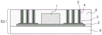
The invention is described below in the context of the preparation of a structure comprising a group III-V base material 2 and a group III-V top material 1 on a substrate 9, as shown in fig. 2, wherein a mesa having a surface lower than the surface of the group III-V base material may be prepared.
The following reference numerals are used throughout the specification:
-a first group III-V material: 1, a step of;
-a second group III-V material: 2;
-a substrate: 9, a step of performing the process;
-one or more dielectric materials: 8, 8;
-metallization: 3, a step of;
-a diffusion barrier layer: 4, a step of;
-a metal filler: 5, a step of;
upper hole O in contact with first material 1 s ;
Lower hole O in contact with second material 2 i 。
From at least one upper hole O S Starting or starting from at least one main upper hole O sp Beginning and starting from at least one secondary upper hole O ss Start to define upper contact C sup 。
From at least one lower hole O I Starting or starting from at least one main lower hole O ip Beginning and starting from at least one secondary lower hole O is Start to define lower contact C inf 。
From at least one main intermediate hole O tp Starting from at least one secondary intermediate hole O ts Start defining intermediate contact C int 。
FIG. 3 shows the result obtained by a method belonging to the first alternative of the inventionGroup III- V materials 1 and 2 are shown on substrate 9, serving as a metallization 3 contacting the bottom metallization, and a contact pad comprising a diffusion barrier layer 4 is made on the metallization 3; the secondary holes are filled with a filler metal 5. The assembly is encapsulated in a dielectric 8. Fig. 3 shows the contact level: lower level N inf Higher level N sup . According to this example, an additional level N is conceivable sup/supl On this level a contact pad filled with a diffusion barrier 7 and a filler metal 6 can be prepared.
The first group III-V material may be composed of a group III-V material such as: inP, in 1-x Ga x As (where 0.ltoreq.x.ltoreq.1), gaAs, inAs, gaSb, in 1-x Ga x Sb、In x Ga 1-x As 1-y P y 、Ga 1-x In x P、In x Ga 1-x As 1-y N y 、B x In y Ga 1-x- y As。
The second III-V material may also be composed of a III-V material such as: inP, in 1-x Ga x As (where 0.ltoreq.x.ltoreq.1), gaAs, inAs, gaSb, in 1-x Ga x Sb、In x Ga 1-x As 1-y P y 、Ga 1-x In x P、In x Ga 1-x As 1-y N y 、B x In y Ga 1-x-y A. Which may be the same or different from the first material.
The substrate may be a silicon substrate, which may for example have a thickness of about a few hundred millimeters (e.g. 200 mm).
According to the invention, the upper horizontal surfaces of the upper contact and the lower contact lie in the same plane.
The figures each show a cross-sectional view of a contact that may be circular or linear.
I) A first alternative of the invention comprises preparing a hole for receiving and contacting a contact bottom metallization.
According to a first embodiment of the method of the invention, comprising a first alternative according to the inventionIs prepared by contacting and then preparing
Contact on standby
A first step of:
this involves packaging a previously fabricated structure comprising a mesa of a first group III-V material 1 on a base surface of group III-V material 2 on a substrate 9.
The dielectric 8 used may be: siN, siO 2 、Al 2 O 3 Planar polymers (e.g., based on benzocyclobutane (BCB)), or SOG "spin-on-glass" polymers: the amorphous dielectric is deposited by centrifugation.
The deposit may be a single layer or multiple layers.
Dielectrics are deposited by PVD (physical vapor deposition), CVD (chemical vapor deposition) and/or ALD (atomic layer deposition). The deposition temperature may be generally 550 ℃ or less, preferably 450 ℃ or less.
The stress of the layer produced may advantageously be less than or equal to 200MPa, preferably less than or equal to 100MPa.
This encapsulation step is shown in fig. 4 a.
And a second step of:
this involves planarizing the dielectric by a CMP operation ("chemical mechanical planarization" or "chemical mechanical polishing") or by dry etching ("etchback") partial removal in the case of planar polymers.
Some polymers have self-leveling properties. I.e. they will fill the lower part first before filling the upper part. However, to ensure complete filling of the cavity, the deposit is thicker than the depth of the cavity. It is necessary to reduce the thickness of the excess deposit. This may be accomplished by dry etching (referred to as "etchback") over the entire wafer.
A localized engraving/etching operation may also be used on the topography prior to CMP.
This planarization step is shown in fig. 4 b.
And a third step of:
this involves making a first lower hole O for lower contact i1 。
The dimensions D1 and D2 may generally be as follows:
the dimension D1 (width of the dielectric on both sides of the mesa of the III-V material 1) is at least 200nm, preferably between 2 and 3 μm.
The dimension D2 (width of the lower hole) may be between 0.5 and 10 μm, and preferably between 1 and 5 μm.
The dimension D3 (thickness of the dielectric) is between 0.5 μm and 5 μm, preferably between 5 and 3 μm.
These holes may be made by dry etching. In this case, the presence of an etch stop layer is optional.
Sequential etching may also be employed:
a first dry etching for etching the part of the dielectric stack, a second dry etching for etching the part of the dielectric stack in the barrier layer (SiN, al 2 O 3 、SiO 2 BCB, SOC, preferably SiN) and then using a dry or wet etch to etch the barrier layer and optional underlying layers, opening on material 2.
The etching operation may be performed directly through a resin for photolithography, or preferably using a hard mask composed of SiN, for example.
Fourth step:
this involves depositing a metallization compatible with the silicon process flow to define the lower contact so that the use of noble metals, i.e., metals not used by the silicon process flow, can be avoided.
Metallization compatible with silicon process flows may be performed according to two options:
-option 1:
(a) Metal 3 (e.g., ni) compatible with silicon process flow is performed 2 P、Ni 3 P, niGe, tiP, tiGe, etc.);
phase stabilization may be performed by an optional heat treatment performed after metal deposition;
(b) Deposition of metal 3 (e.g., ni, ti, and alloys such as NiPt, niTi, niCo, etc.) compatible with silicon process flow is performed;
-option 2: performing a deposition of a metal (Ni, ti, and alloys thereof) compatible with the silicon process flow; a heat treatment is then performed in order to effect a solid state reaction between the metal and the group III-V material, resulting in the formation of one or more intermetallic compounds.
The deposition temperature is preferably 450 ℃ or less.
The annealing temperature is preferably 450 ℃ or less.
According to option 1, a metal or intermetallic compound is deposited and the work function of the intermetallic compound is utilized. In this case, annealing is used to heal the interface defect and crystallize the metal or compound.
According to option 2, a metal is deposited and reacted to form an intermetallic compound having a desired work function. In this case, annealing is used for the solid state reaction.
The selective removal of unreacted metal may be performed after the heat treatment.
All of these steps are shown in fig. 4 d.
Fifth step:
this involves filling the first lower hole and a CMP operation to manufacture the connection pad. The lower hole is filled twice:
deposition of a diffusion barrier/keying layer or nucleation layer 4. It may consist of TiN, ti/TiN, taN, ta/TaN or W deposited by CVD, PVD or ALD;
-deposition of the filler metal 5 (W, cu, alCu, alSi) by CVD, ECD or PVD deposition.
Finally, a CMP operation is performed to remove the pad contacts. Because metal is present at the top of the cavity between the two pads, a short circuit is unavoidable. The CMP operation makes it possible to remove only the metal from the pads and thus to remove them from contact.
All of these steps are shown in fig. 4 e.
Sixth step:
this involves the encapsulation step of the assembly defined above with dielectric 8. The thickness D5 of the dielectric above the material 1 may generally be between 200nm and 1 μm, and preferably between 200nm and 500 nm. The dielectrics used may be: siN, siO 2 、Al 2 O 3 Planar polymers (e.g., BCB, SOG). Deposition ofThe article may be a single layer or multiple layers. They are deposited by PVD, CVD and/or ALD.
The deposition temperature is 450 ℃ or less, preferably 300 ℃ or less.
This step is shown in fig. 4 f.
If the phase stabilization or heat treatment operation has not been performed to form one or more intermetallic compounds, it may be performed at the end of this step.
Seventh step:
this involves making a second lower hole O for lower contact i2 And a hole O for upper contact s 。
These holes may be made by dry etching. In this case, the presence of an etch stop layer is optional.
Sequential etching may also be employed: a first dry etching for etching the part of the dielectric stack, a second dry etching for etching the part of the dielectric stack in the barrier layer (SiN, al 2 O 3 、SiO 2 BCB, SOC, preferably SiN) and then etching the barrier layer and optional underlying layer using a dry or wet etch, opening in material 1.
The etching operation may be performed directly through a resin for photolithography, or preferably using a hard mask composed of SiN, for example.
The dimension D2 (width of the upper aperture) may be between 0.5 and 10 μm, and preferably between 1 and 5 μm.
This step is shown in fig. 4 g.
Eighth step:
this involves depositing a metallization compatible with the silicon process flow to define the lower contact and the upper contact so that the use of noble metals, i.e., metals not used by the silicon process flow, can be avoided.
Metallization compatible with silicon process flows may be performed according to two options:
-option 1:
(a) Metal 3 (e.g., ni) compatible with silicon process flow is performed 2 P、Ni 3 P, niGe, tiP, tiGe, etc.);
phase stabilization may be performed by an optional heat treatment performed after metal deposition;
(b) Deposition of metal 3 (e.g., ni, ti, and alloys such as NiPt, niTi, niCo, etc.) compatible with silicon process flow is performed;
-option 2: performing a deposition of a metal (Ni, ti, and alloys thereof) compatible with the silicon process flow; a heat treatment is then performed in order to effect a solid state reaction between the metal and the group III-V material, resulting in the formation of one or more intermetallic compounds.
The deposition temperature is preferably 450 ℃ or less.
The annealing temperature is preferably 450 ℃ or less.
According to option 1, a metal or intermetallic compound is deposited and the work function of the intermetallic compound is utilized. In this case, annealing is used to heal the interface defect and crystallize the metal or compound.
This step is shown in fig. 4 h.
Ninth step:
this involves filling the lower and upper holes and CMP operations to make the connection pads. Filling of the lower and upper holes was performed twice:
deposition of a diffusion barrier/keying layer or nucleation layer 4. It may consist of TiN, ti/TiN, taN, ta/TaN or W deposited by CVD, PVD or ALD;
-deposition of the filler metal 5 (W, cu, alCu, alSi) by CVD, ECD or PVD deposition.
Finally, a CMP operation is performed to remove the pad contacts. Because metal is present at the top of the cavity between the two pads, a short circuit is unavoidable. The CMP operation makes it possible to remove only the metal from the pads and thus to remove them from contact.
All these steps are shown in fig. 4i, fig. 4i showing the upper contact C sup And under contact C inf The level of the two metallizations 3.
An alternative to the embodiment described in this first example comprises sequentially defining the contacted cavities depicted in fig. 4 c-4 d and then in fig. 4 g-4 h, but defining the pad cavities depicted in fig. 4e and 4i in a single step.
According to a second embodiment of the method of the invention, comprising preparing an upper contact and then a lower contact according to the first alternative of the invention
Is provided with a lower contact
A first step of:
this involves packaging a previously fabricated structure comprising a mesa of a first group III-V material 1 on a base surface of group III-V material 2 on a substrate 9.
The dielectric 8 used may be: siN, siO 2 、Al 2 O 3 Planar polymers (e.g., based on benzocyclobutane (BCB)), or SOG "spin-on-glass" polymers: the amorphous dielectric is deposited by centrifugation.
The deposit may be a single layer or multiple layers.
Dielectrics are deposited by PVD (physical vapor deposition), CVD (chemical vapor deposition) and/or ALD (atomic layer deposition). The deposition temperature may be generally 550 ℃ or less, preferably 450 ℃ or less.
The stress of the layer produced can advantageously be less than or equal to 200MPa, preferably less than or equal to 100MPa.
This encapsulation step is shown in fig. 5 a.
And a second step of:
this involves planarizing the dielectric by a CMP operation ("chemical mechanical planarization" or "chemical mechanical polishing") or by dry etching ("etchback") partial removal in the case of planar polymers.
Some polymers have self-leveling properties. I.e. they will fill the lower part first before filling the upper part. However, to ensure complete filling of the cavity, the deposit is thicker than the depth of the cavity. It is necessary to reduce the thickness of the excess deposit. This may be accomplished by dry etching (referred to as "etchback") over the entire wafer.
A localized engraving/etching operation may also be used on the topography prior to CMP.
This planarization step is shown in fig. 5 b.
And a third step of:
this involves making an upper hole O for the upper contact s 。
These holes may be made by dry etching. In this case, the presence of an etch stop layer is optional.
Sequential etching may also be employed:
a first dry etching for etching the part of the dielectric stack, a second dry etching for etching the part of the dielectric stack in the barrier layer (SiN, al 2 O 3 、SiO 2 BCB, SOC, preferably SiN) and then etching the barrier layer and optional underlying layer using a dry or wet etch, opening in material 1.
The etching operation may be performed directly through a resin for photolithography, or preferably using a hard mask composed of SiN, for example.
This step of making the holes is shown in fig. 5 c.
Fourth step:
this involves depositing a metallization compatible with the silicon process flow to define the upper contact so that the use of noble metals, i.e., metals not used by the silicon process flow, can be avoided.
Metallization compatible with silicon process flows may be performed according to two options:
-option 1:
(a) Metal 3 (e.g., ni) compatible with silicon process flow is performed 2 P、Ni 3 P, niGe, tiP, tiGe, etc.);
phase stabilization may be performed by an optional heat treatment performed after metal deposition;
(b) Deposition of metal 3 (e.g., ni, ti, and alloys such as NiPt, niTi, niCo, etc.) compatible with silicon process flow is performed;
-option 2: performing a deposition of a metal (Ni, ti, and alloys thereof) compatible with the silicon process flow; a heat treatment is then performed in order to effect a solid state reaction between the metal and the group III-V material, resulting in the formation of one or more intermetallic compounds.
The deposition temperature is preferably 450 ℃ or less.
The annealing temperature is preferably 450 ℃ or less.
According to option 1, a metal or intermetallic compound is deposited and the work function of the intermetallic compound is utilized. In this case, annealing is used to heal the interface defect and crystallize the metal or compound.
This step is shown in fig. 5 d.
Fifth step:
this involves filling the upper holes and CMP operations to make the connection pads. Filling of the upper hole was performed twice:
deposition of a diffusion barrier/keying layer or nucleation layer 4. It may consist of TiN, ti/TiN, taN, ta/TaN or W deposited by CVD, PVD or ALD;
-deposition of the filler metal 5 (W, cu, alCu, alSi) by CVD, ECD or PVD deposition.
Finally, a CMP operation is performed to remove the pad contacts. Because metal is present at the top of the cavity between the two pads, a short circuit is unavoidable. The CMP operation makes it possible to remove only the metal from the pads and thus to remove them from contact.
All these steps are shown in fig. 5e, fig. 5e showing the level of the two metallizations 3 in the upper contact.
Sixth step:
this involves making a lower hole O for lower contact i 。
These holes may be made by dry etching. In this case, the presence of an etch stop layer is optional.
Sequential etching may also be employed:
a first dry etching for etching the part of the dielectric stack, a second dry etching for etching the part of the dielectric stack in the barrier layer (SiN, al 2 O 3 、SiO 2 BCB, SOC, preferably SiN) and then using a dry or wet etch to etch the barrier layer and optional underlying layers, opening on material 2.
The etching operation may be performed directly through a resin for photolithography, or preferably using a hard mask composed of SiN, for example.
This step of making the holes is shown in fig. 5 f.
Seventh step:
this involves depositing a metallization compatible with the silicon process flow to define the lower contact so that the use of noble metals, i.e., metals not used by the silicon process flow, can be avoided.
Metallization compatible with silicon process flows may be performed according to two options:
-option 1:
(a) Metal 3 (e.g., ni) compatible with silicon process flow is performed 2 P、Ni 3 P, niGe, tiP, tiGe, etc.);
phase stabilization may be performed by an optional heat treatment performed after metal deposition;
(b) Deposition of metal 3 (e.g., ni, ti, and alloys such as NiPt, niTi, niCo, etc.) compatible with silicon process flow is performed;
-option 2: performing a deposition of a metal (Ni, ti, and alloys thereof) compatible with the silicon process flow; a heat treatment is then performed in order to effect a solid state reaction between the metal and the group III-V material, resulting in the formation of one or more intermetallic compounds.
The deposition temperature is preferably 450 ℃ or less.
The annealing temperature is preferably 450 ℃ or less.
According to option 1, a metal or intermetallic compound is deposited and the work function of the intermetallic compound is utilized. In this case, annealing is used to heal the interface defect and crystallize the metal or compound.
This step is shown in fig. 5 g.
Eighth step:
this involves filling the lower holes and CMP operations to make the connection pads. The lower hole is filled twice:
deposition of a diffusion barrier/keying layer or nucleation layer 4. It may consist of TiN, ti/TiN, taN, ta/TaN or W deposited by CVD, PVD or ALD;
-deposition of the filler metal 5 (W, cu, alCu, alSi) by CVD, ECD or PVD deposition.
Finally, a CMP operation is performed to remove the pad contacts. Because metal is present at the top of the cavity between the two pads, a short circuit is unavoidable. The CMP operation makes it possible to remove only the metal from the pads and thus to remove them from contact.
All these operations are shown in fig. 5h, fig. 5h showing the level of the two metallizations 3 in the lower contact.
An alternative to the embodiment described in this second example comprises cavities that sequentially open the contacts described in fig. 5 c-5 d and then in fig. 5 f-5 g, but open the pad cavities described in fig. 5e and 5h in a single step.
According to a third embodiment of the method of the invention, comprising the simultaneous preparation of the upper contact and of the lower contact according to the first alternative of the invention
And (3) lower contact:
first step:
This involves packaging a previously fabricated structure comprising a mesa of a first group III-V material 1 on a base surface of group III-V material 2 on a substrate 9.
The dielectric 8 used may be: siN, siO 2 、Al 2 O 3 Planar polymers (e.g., based on benzocyclobutane (BCB)), or SOG "spin-on-glass" polymers: the amorphous dielectric is deposited by centrifugation.
The deposit may be a single layer or multiple layers.
Dielectrics are deposited by PVD (physical vapor deposition), CVD (chemical vapor deposition) and/or ALD (atomic layer deposition). The deposition temperature may be generally 550 ℃ or less, preferably 450 ℃ or less.
The stress of the layer produced can advantageously be less than or equal to 200MPa, preferably less than or equal to 100MPa.
This encapsulation step is shown in fig. 6 a.
A second step of:
This involves planarizing the dielectric by a CMP operation ("chemical mechanical planarization" or "chemical mechanical polishing") or by dry etching ("etchback") partial removal in the case of planar polymers.
Some polymers have self-leveling properties. I.e. they will fill the lower part first before filling the upper part. However, to ensure complete filling of the cavity, the deposit is thicker than the depth of the cavity. It is necessary to reduce the thickness of the excess deposit. This may be accomplished by dry etching (referred to as "etchback") over the entire wafer.
A localized engraving/etching operation may also be used on the topography prior to CMP.
This planarization step is shown in fig. 6 b.
And a third step of:
this involves making an upper hole O for the upper contact s And a lower hole O for lower contact i 。
These holes may be made by dry etching. In this case, the presence of an etch stop layer is optional.
Sequential etching may also be employed:
a first dry etching for etching the part of the dielectric stack, a second dry etching for etching the part of the dielectric stack in the barrier layer (SiN, al 2 O 3 、SiO 2 BCB, SOC, preferably SiN) and then using a dry or wet etch to etch the barrier layer and optional underlying layers, opening on material 1 and material 2.
The etching operation may be performed directly through a resin for photolithography, or preferably using a hard mask composed of SiN, for example.
This step of making the holes is shown in fig. 6 c.
Fourth step:
this involves depositing a metallization compatible with the silicon process flow to define the upper and lower contacts so that the use of noble metals, i.e., metals not used by the silicon process flow, can be avoided.
Metallization compatible with silicon process flows may be performed according to two options:
-option 1:
(a) Metal 3 (e.g., ni) compatible with silicon process flow is performed 2 P、Ni 3 P, niGe, tiP, tiGe, etc.);
phase stabilization may be performed by an optional heat treatment performed after metal deposition;
(b) Deposition of metal 3 (e.g., ni, ti, and alloys such as NiPt, niTi, niCo, etc.) compatible with silicon process flow is performed;
-option 2: performing a deposition of a metal (Ni, ti, and alloys thereof) compatible with the silicon process flow; a heat treatment is then performed in order to effect a solid state reaction between the metal and the group III-V material, resulting in the formation of one or more intermetallic compounds.
The deposition temperature is preferably 450 ℃ or less.
The annealing temperature is preferably 450 ℃ or less.
According to option 1, a metal or intermetallic compound is deposited and the work function of the intermetallic compound is utilized. In this case, annealing is used to heal the interface defect and crystallize the metal or compound.
This step is shown in fig. 6 d.
Fifth step:
this involves filling the upper and lower holes and CMP operations to make the connection pads. Simultaneous filling of the upper and lower holes is performed twice:
deposition of a diffusion barrier/keying layer or nucleation layer 4. It may consist of TiN, ti/TiN, taN, ta/TaN or W deposited by CVD, PVD or ALD;
-deposition of the filler metal 5 (W, cu, alCu, alSi) by CVD, ECD or PVD deposition.
Finally, a CMP operation is performed to remove the pad contacts. Because metal is present at the top of the cavity between the two pads, a short circuit is unavoidable. The CMP operation makes it possible to remove only the metal from the pads and thus to remove them from contact.
This step is shown in fig. 6 e.
A variant of the first embodiment of the method according to the invention comprises the preparation of the lower contact and then the preparation of the upper contact according to the first alternative of the invention, comprising the addition of an engraving step to remove the metallization layer 3 present in the low-level pad (outside). The metallization layer 3 increases the interface and may therefore be detrimental from an electrical point of view.
This variant is described below and comprises the same steps as those described in fig. 4a to 4f and is shown in fig. 7f to 7i, the reference numerals remaining the same for a better understanding.
An assembly was prepared in which the pads of the lower contact were prefabricated, encapsulated in a dielectric 8, as shown in fig. 7 f.
Holes O are then made at the level of the first material 1 s For upper contact as shown in fig. 7 g. These holes may be made by dry etching. In this case, the presence of an etch stop layer is optional.
Sequential etching may also be performed:
A first dry etching for etching the part of the dielectric stack, a second dry etching for etching the part of the dielectric stack in the barrier layer (SiN, al 2 O 3 、SiO 2 BCB, SOC, preferably SiN) and then etching the barrier layer and optional underlying layer using a dry or wet etch, opening in material 1.
The etching operation may be performed directly through a resin for photolithography, or preferably using a hard mask composed of SiN, for example.
Metallization compatible with the silicon process flow is then deposited to define the upper and lower contacts so that the use of noble metals, i.e., metals not used by the silicon process flow, can be avoided.
Metallization compatible with silicon process flows may be performed according to two options:
-option 1:
(a) Metal 3 (e.g., ni) compatible with silicon process flow is performed 2 P、Ni 3 P, niGe, tiP, tiGe, etc.);
phase stabilization may be performed by an optional heat treatment performed after metal deposition;
(b) Deposition of metal 3 (e.g., ni, ti, and alloys such as NiPt, niTi, niCo, etc.) compatible with silicon process flow is performed;
-option 2: performing a deposition of a metal (Ni, ti, and alloys thereof) compatible with the silicon process flow; a heat treatment is then performed in order to effect a solid state reaction between the metal and the group III-V material, resulting in the formation of one or more intermetallic compounds.
The deposition temperature is preferably 450 ℃ or less.
The annealing temperature is preferably 450 ℃ or less.
According to option 1, a metal or intermetallic compound is deposited and the work function of the intermetallic compound is utilized. In this case, annealing is used to heal the interface defect and crystallize the metal or compound.
This step is shown in fig. 7 h.
A CMP-type operation is then performed to remove excess metal at the top of the dielectric stack, leaving only the holes O present, as shown in fig. 7i s Layer 3 at the level of (2).
Then a second lower hole O for lower contact is manufactured i2 As shown in fig. 7 j. These holes may be made by dry etching. In this case, the presence of an etch stop layer is optional.
Sequential etching may also be used:
dielectric stack etch for opening external pads of lower contacts on material:
filling material to perform one etch up to low level pad: and (5) dry etching. In this case, the presence of an etch stop layer is optional.
Sequential etching: a first dry etching for etching the part of the dielectric stack, a second dry etching for etching the part of the dielectric stack in the barrier layer (SiN, al 2 O 3 、SiO 2 BCB, SOC, preferably SiN) and then etching the barrier layer and optional underlying layer using a dry or wet etch, opening in the fill material of the underlying level pad.
The etching operation may be performed directly through a resin for photolithography, or preferably using a hard mask composed of SiN, for example.
Then, upper pads and upper portions of the lower pads are prepared on top of the first portion of the previously prepared lower pad. By filling all holes O s And O i2 To do this.
Upper hole O s And lower hole O i2 Is performed twice:
deposition of a diffusion barrier/keying layer or nucleation layer 4. It may consist of TiN, ti/TiN, taN, ta/TaN or W deposited by CVD, PVD or ALD;
-deposition of the filler metal 5 (W, cu, alCu, alSi) by CVD, ECD or PVD deposition.
Finally, a CMP operation is performed to remove the pad contacts. Because metal is present at the top of the cavity between the two pads, a short circuit is unavoidable. The CMP operation makes it possible to remove only the metal from the pads and thus to remove them from contact.
This filling operation is shown in fig. 7 k.
Alternatives to the holes of the pads described in the three embodiments above include integrating the contact pads by a dual damascene process. Dual damascene is a two-step etching process in which metal filling and CMP for removing excess metal (one or both barrier + filling) are performed consecutively in a single step. This generally makes it possible to prepare a via and a line leading to the via: connections and paths.
This alternative is schematically shown according to the embodiment shown in fig. 8b to 8 e. The encapsulation and smoothing assembly shown in fig. 8b is prepared in a similar manner as described above.
Referred to as a second lower hole O i2 Is made by partially etching the dielectric at the top of the lower hole. Dry etching may be used. In this case, the presence of an etch stop layer is optional.
The etching operation may be performed directly through a resin for photolithography, or using a hard mask composed of SiN, for example.
This step is shown in fig. 8 c.
A second operation of etching the dielectric is performed to fabricate upper hole O s And is called a first lower hole O i1 Lower portion of the lower hole of (2).
These holes may be made by dry etching. In this case, the presence of an etch stop layer is optional.
Sequential etching may also be used:
dielectric stack etch for opening external pads of lower contacts on material:
filling material to perform one etch up to low level pad: and (5) dry etching. In this case, the presence of an etch stop layer is optional.
Sequential etching: a first dry etching for etching the part of the dielectric stack, a second dry etching for etching the part of the dielectric stack in the barrier layer (SiN, al 2 O 3 、SiO 2 BCB, SOC, preferably SiN) and then etching the barrier layer and optional underlying layer using a dry or wet etch, opening in the fill material of the underlying level pad.
The etching operation may be performed directly through a resin for photolithography, or preferably using a hard mask composed of SiN, for example.
This step is shown in fig. 8 d.
Pads for upper and lower contacts were then prepared by filling. Upper hole O s And lower hole O i2 And O i2 Is performed twice:
deposition of a diffusion barrier/keying layer or nucleation layer 4. It may consist of TiN, ti/TiN, taN, ta/TaN or W deposited by CVD, PVD or ALD;
-deposition of the filler metal 5 (W, cu, alCu, alSi) by CVD, ECD or PVD deposition.
Finally, a CMP operation is performed to remove the pad contacts. Because metal is present at the top of the cavity between the two pads, a short circuit is unavoidable. The CMP operation makes it possible to remove only the metal from the pads and thus to remove them from contact.
This filling operation is shown in fig. 8 e.
All the embodiments described in the previous examples can be supplemented with additional integration levels.
Thus, additional steps may be performed by performing additional deposition of dielectric 8, then additional upper and lower holes are made by etching and filling these holes to define contact C inf/supl And C sup/supl As shown in fig. 9.
For this purpose, in the additional upper and lower holes, a barrier layer 7 is deposited, which may be TiN, ti/TiN, taN, ta/TaN, W and filled with a metal 6, which may be W, cu or Al, alCu, alSi.
Examples of laser elements prepared by the method of the present invention:
the method of the invention advantageously makes it possible to prepare lasers based on group III-V materials:
SiO 2 comprises a silicon guide 91 on top of which the following are prepared:
a substrate of a second group III-V material 2, which material 2 may be n-doped InP, and a mesa 1 comprising a multiple quantum well structure, which may be made of InGaAsP and p-doped InGaAs layers with different doping, the properties of the group III-V material determining the emission wavelength;
the dielectric 8 may be SiN, siO 2 Or planar polymers based on BCB, for example;
the contact bottom metallization 3 may be, for example, ni, ti or an alloy thereof (Ni 2 P、Ni 3 P, niGe, tiP, tiGe, etc.);
the F diffusion barrier and/or W keying layer 4 may be TiN, ti/TiN, taN, ta/TaN, W,
the filler metal 5 may be Cu or Al, alCu, alSi.
An example of this laser is shown in fig. 10.
Examples of VCSEL type vertical-emitting laser elements:
recall that in general, a vertical cavity surface emitting laser diode or VCSEL is a semiconductor laser diode that emits a laser beam perpendicular to the surface, unlike conventional edge emitting semiconductor lasers.
Examples of the laser mainly include the same types of structures as those described in the foregoing examples.
However, to allow laser radiation to be emitted at the top of the structure, the upper contact is made circular.
An example of this element comprises a silicon substrate 9 on top of which the following are prepared: a substrate of a second group III-V material 2, which material 2 may be n-doped InP, and a mesa 1 comprising a multiple quantum well structure, which may determine the emission wavelength based on InGaAsP, alGaAs, gaAs, inGaAsN and p-doped InGaAs layers, the properties of the group III-V material.
The dielectric 8 may be SiN, siO 2 Or planar polymers based on BCB, for example.
The contact bottom metallization 3 may be, for example, ni, ti or an alloy thereof (Ni 2 P、Ni 3 P, niGe, tiP, tiGe, etc.).
The F diffusion barrier layer and/or the W keying layer 4 may be TiN, ti/TiN, taN, ta/TaN, W.
The filler metal 5 may be Cu or Al, alCu, alSi.
Due to contact C on the circle sup The laser beam may be extracted from the upper surface of the element.
An example of this laser is shown in fig. 11.
II) A second alternative of the invention comprises making the primary and secondary holes
According to this second alternative described above, the contact pads in the primary hole bottom metallization and the secondary holes are defined. Thus, the contact comprises at least a hole bottom metallization and a contact pad in contact with said metallization.
Fig. 12 shows an example of an assembly obtained by a method belonging to the first alternative of the invention and shows on a substrate 9 the III- V materials 1 and 2, acting as a contact bottom metallization 3, a contact pad comprising a diffusion barrier layer 4 made on the metallization 3; the secondary holes are filled with a filler metal 5. All encapsulated in dielectric 8. Fig. 12 shows the contact level: lower level N inf Higher level N sup . According to this example, an additional level N is conceivable sup/supl On this level a contact pad filled with a diffusion barrier 7 and a filler metal 6 can be prepared.
The first group III-V material may be composed of a group III-V material such as: inP, in 1-x Ga x As (where 0.ltoreq.x.ltoreq.1), gaAs, inAs, gaSb, in 1-x Ga x Sb、In x Ga 1-x As 1-y P y 、Ga 1-x In x P、In x Ga 1-x As 1-y N y 、B x In y Ga 1-x- y As。
The second III-V material may also be composed of a III-V material such as: inP, in 1-x Ga x As (where 0.ltoreq.x.ltoreq.1), gaAs, inAs, gaSb, in 1-x Ga x Sb、In x Ga 1-x As 1-y P y 、Ga 1-x In x P、In x Ga 1-x As 1-y N y 、B x In y Ga 1-x-y A. Which may be the same or different from the first material.
The substrate may be a silicon substrate, which may for example have a thickness of about a few hundred millimeters (e.g. 200 mm).
According to a first embodiment of the process of the invention, the lower contact is prepared and then prepared according to a second alternative of the invention
Contact on standby
First step :
This involves packaging a previously fabricated structure comprising a mesa of a first group III-V material 1 on a base surface of group III-V material 2 on a substrate 9.
The dielectric 8 used may be: siN, siO 2 、Al 2 O 3 Planar polymers (e.g., based on benzocyclobutane (BCB)), or SOG "spin-on-glass" polymers: the amorphous dielectric is deposited by centrifugation.
The deposit may be a single layer or multiple layers.
Dielectrics are deposited by PVD (physical vapor deposition), CVD (chemical vapor deposition) and/or ALD (atomic layer deposition). The deposition temperature may be generally 550 ℃ or less, preferably 450 ℃ or less.
The stress of the layer produced can advantageously be less than or equal to 200MPa, preferably less than or equal to 100MPa.
This encapsulation step is shown in fig. 13 a.
A second step of:
This involves planarizing the dielectric by a CMP operation ("chemical mechanical planarization" or "chemical mechanical polishing") or by dry etching ("etchback") partial removal in the case of planar polymers.
Some polymers have self-leveling properties. I.e. they will fill the lower part first before filling the upper part. However, to ensure complete filling of the cavity, the deposit is thicker than the depth of the cavity. It is necessary to reduce the thickness of the excess deposit. This may be accomplished by dry etching (referred to as "etchback") over the entire wafer.
A localized engraving/etching operation may also be used on the topography prior to CMP.
This planarization step is shown in fig. 13 b.
And a third step of:
this involves making a main lower hole O for lower contact ip 。
The dimensions D1, D2, D3 and D4 may generally be as follows:
the dimension D1 (width of the dielectric on both sides of the mesa of the III-V material 1) is at least 200nm, preferably between 2 and 3 μm.
The dimension D2 (width of the main lower hole) may be between 20 and 50 μm.
The dimension D3 (thickness of the dielectric) is between 0.5 μm and 5 μm, preferably between 5 and 3 μm.
The dimension D4 (intermediate width between the two main lower holes) may be between 0.5 μm and 10 μm, preferably between 1 and 5 μm.
For this purpose, a partial etching of the dielectric (in the case of several layers) is performed to open on the III-V material 2. The etching may be performed once by a dry etching operation up to the group III-V material 2. In this case, the presence of an etch stop layer is optional.
Sequential etching operations may also be performed: a first dry etching for etching the part of the dielectric stack, a second dry etching for etching the part of the dielectric stack in the barrier layer (SiN, al 2 O 3 、SiO 2 BCB, SOC, preferably SiN) and then using a dry or wet etch to etch the barrier layer and optional underlying layers, opening on the III-V material 2.
The etching operation may be performed directly through a resin for photolithography, or preferably using a hard mask composed of SiN, for example.
This step of making the holes is shown in fig. 13 c.
Fourth step:
this involves depositing a metallization compatible with the silicon process flow to define the lower contact so that the use of noble metals, i.e., metals not used by the silicon process flow, can be avoided.
Metallization compatible with silicon process flows may be performed according to two options:
-option 1:
(a) Metal 3 (e.g., ni) compatible with silicon process flow is performed 2 P、Ni 3 P, niGe, tiP, tiGe, etc.);
phase stabilization may be performed by an optional heat treatment performed after metal deposition;
(b) Deposition of metal 3 (e.g., ni, ti, and alloys such as NiPt, niTi, niCo, etc.) compatible with silicon process flow is performed;
-option 2: performing a deposition of a metal (Ni, ti, and alloys thereof) compatible with the silicon process flow; a heat treatment is then performed in order to effect a solid state reaction between the metal and the group III-V material, resulting in the formation of one or more intermetallic compounds.
The deposition temperature is preferably 450 ℃ or less.
The annealing temperature is preferably 450 ℃ or less.
According to option 1, a metal or intermetallic compound is deposited and the work function of the intermetallic compound is utilized. In this case, annealing is used to heal the interface defect and crystallize the metal or compound.
According to option 2, a metal is deposited and reacted to form an intermetallic compound having a desired work function. In this case, annealing is used for the solid state reaction.
The selective removal of unreacted metal may be performed after the heat treatment.
The assembly E1 shown in fig. 13d is then obtained.
Fifth step:
this involves the encapsulation step of the component E1 with the dielectric 8. The dielectrics used may be: siN, siO 2 、Al 2 O 3 Planar polymers (e.g., BCB, SOG). The deposit may be a single layer or multiple layers. They are deposited by PVD, CVD and/or ALD;
the deposition temperature is 450 ℃ or less, preferably 300 ℃ or less.
This step is shown in fig. 13 e.
If the phase stabilization or heat treatment operation is not performed at the end of the fourth step to form one or more intermetallic compounds, it may be performed at the end of the step.
Sixth step:
this involves planarizing the dielectric by a CMP operation or an "etchback" type operation in the case of a planar polymer.
CMP or "etchback" planarization may be performed:
-if in the fourth step no selective removal is performed, until the metal is removed;
if in the fourth step no selective removal is performed and if no CMP or "etchback" type operation of the metal can be performed, stopping on the metal. A step of selective metal removal can then be performed to obtain the structure shown in fig. 13 f;
If in the fourth step the selective removal is performed, until the structure shown in fig. 13f is obtained.
Typically, the height D5 (thickness of the dielectric on top of the III-V material 1) shown may be between 200nm and 1 μm.
If the phase stabilization or heat treatment operation is not performed at the end of the fourth step or at the end of the fifth step to form one or more intermetallic compounds, it may be performed at the end of the step.
Seventh step:
this relates to the last lower hole O for the connection pad is1 Is performed according to the operation of (a). For this purpose, an etching of the dielectric stack is performed to provide a metallization 3 at a lower levelAn opening.
Etching is performed once until metallization: and (5) dry etching. In this case, the presence of an etch stop layer is optional.
Sequential etching may be employed: a first dry etching for etching the part of the dielectric stack, a second dry etching for etching the part of the dielectric stack in the barrier layer (SiN, al 2 O 3 、SiO 2 BCB, SOC, preferably SiN) and then using a dry or wet etch to etch the barrier layer and optional underlying layers, opening on the metallization 3.
The etching operation may be performed directly through a resin for photolithography, or using a hard mask composed of SiN, for example. In general, the dimension D6 (width of the sub-lower hole) of the illustrated dielectric may be between 0.5 μm and 5 μm, and preferably between 1 μm and 3 μm. This step is shown in fig. 13 g.
Eighth step:
this involves filling the sub-down holes and CMP operations to make the connection pads. Filling of the lower hole was performed twice:
deposition of a diffusion barrier/keying layer or nucleation layer 4. It may consist of TiN, ti/TiN, taN, ta/TaN or W deposited by CVD, PVD or ALD;
-deposition of the filler metal 5 (W, cu, alCu, alSi) by CVD, ECD or PVD deposition.
Finally, a CMP operation is performed to remove the pad contacts. Because metal is present at the top of the cavity between the two pads, a short circuit is unavoidable. The CMP operation makes it possible to remove only the metal from the pads and thus to remove them from contact.
A new assembly E2 is produced. All of these steps are shown in fig. 13 h.
Ninth step:
this involves the operation of encapsulation with dielectric 8. The dielectrics used may be: siN, siO 2 、Al 2 O 3 Planar polymers (e.g., BCB, SOG). The deposit may be a single layer or multiple layers. The dielectric is deposited by PVD, CVD, and/or ALD. The deposition temperature is 450 ℃ or less, preferably 300 ℃ or less. Typically, the dielectric is shownThe height D7 of the mass may be between 200nm and 1 μm, and preferably between 200nm and 500 nm. This step is shown in fig. 13 i.
Tenth step:
this involves making a main upper hole O for forming an upper contact sp 。
This involves etching the dielectric stack to open on the III-V material 1. The etching may be performed once by dry etching up to the group III-V material 1. In this case, the presence of an etch stop layer is optional.
Sequential etching may be employed: a first dry etching for etching the part of the dielectric stack, a second dry etching for etching the part of the dielectric stack in the barrier layer (SiN, al 2 O 3 、SiO 2 BCB, SOC, preferably SiN) and then using a dry or wet etch to etch the barrier layer and optional underlying layers, opening on the III-V material 1.
The etching operation may be performed directly through a resin for photolithography, or preferably using a hard mask composed of SiN, for example.
This step is shown in fig. 13 j.
Eleventh step:
this involves the deposition of a metallization 3 compatible with the silicon process flow for the upper contact. Metallization compatible with silicon process flows can be performed in two ways:
-option 1:
(a) Metal 3 (e.g., ni) compatible with silicon process flow is performed 2 P、Ni 3 P, niGe, tiP, tiGe, etc.);
phase stabilization may be performed by an optional heat treatment performed after metal deposition;
(b) Deposition of metal 3 (e.g., ni, ti, and alloys such as NiPt, niTi, niCo, etc.) compatible with silicon process flow is performed;
-option 2: performing a deposition of a metal (Ni, ti, and alloys thereof) compatible with the silicon process flow; a heat treatment is then performed in order to effect a solid state reaction between the metal and the group III-V material, resulting in the formation of one or more intermetallic compounds.
The annealing temperature is preferably 450 ℃ or less.
The selective removal of unreacted metal may be performed after the heat treatment. A third component E3 is obtained.
This step is shown in fig. 13 k.
Twelfth step:
this involves packaging the third component E3. The dielectrics used may be: siN, siO 2 、Al 2 O 3 Planar polymers (e.g., BCB), SOG. The deposit may be a single layer or multiple layers. They are deposited by PVD, CVD and/or ALD. The deposition temperature is 450 ℃ or less, preferably 300 ℃ or less.
This step is shown in fig. 13 l.
If the phase stabilization or heat treatment operation is not performed at the end of the eleventh step to form one or more intermetallic compounds, it may be performed at the end of the step.
Thirteenth step:
this involves a planarization operation.
Planarization or etchback may be performed:
-if in the eleventh step no selective removal is performed, until the metal is removed;
if in the eleventh step no selective removal is performed and if no CMP or "etchback" type operation of the metal can be performed, stopping on the metal. A step of selective metal removal can then be performed to obtain the structure shown in fig. 13 m;
If the selective removal is performed in the eleventh step, until the structure shown in fig. 13m is obtained.
If the phase stabilization or heat treatment operation is not performed at the end of the eleventh step or at the end of the twelfth step to form one or more intermetallic compounds, it may be performed at the end of the step.
Fourteenth step:
this involves making a secondary upper hole O ss And at least contact pads in contact underIs provided with an additional upper hole O at the top is2 。
This involves etching the dielectric stack to open up the metallization at the upper contact level and the contact pads of the lower contact.
The etching is performed once by dry etching up to metallization 3 and up to the pad of the lower level. In this case, the presence of an etch stop layer is optional.
Sequential etching operations may be performed: first dry etching is used to etch portions of the dielectric stack, barrier layers (SiN, al) on pads of upper and lower contacts bottom metallization 2 O 3 、SiO 2 BCB, SOC, preferably SiN).
A dry or wet etch may be used to etch the barrier layer and optional underlying layers to open up the metallization 3.
The etching operation may be performed directly through a resin for photolithography, or using a hard mask composed of SiN, for example.
This step is shown in fig. 13 n.
Fifteenth step:
this involves filling the holes defined in the previous step.
The filling of the holes was performed twice:
deposition of a diffusion barrier/keying layer or nucleation layer. It may consist of TiN, ti/TiN, taN, ta/TaN or W deposited by CVD, PVD or ALD;
-deposition of the filler metal (W, cu, alCu, alSi, etc.) by CVD, ECD or PVD deposition.
Finally, a CMP operation is performed to remove the pad contacts.
This step is shown in FIG. 13o and allows the upper contact C to be made sup And lower contact C inf 。
An alternative to the first method embodiment may include sequentially preparing primary apertures coupled to secondary apertures prepared simultaneously.
According to a second embodiment of the method of the invention, comprising preparing an upper contact and then preparing according to a second alternative of the invention
Is provided with a lower contact
A first step of:
this involves packaging a previously fabricated structure comprising a mesa of a first group III-V material 1 on a base surface of group III-V material 2 on a substrate 9.
The dielectric 8 used may be: siN, siO 2 、Al 2 O 3 Planar polymers (e.g., BCB, SOG).
The deposit may be a single layer or multiple layers.
The dielectric is deposited by PVD, CVD, and/or ALD. The deposition temperature may be generally 450 ℃ or less, preferably 300 ℃ or less.
The stress of the layer produced may be 200MPa or less, preferably 100MPa or less. This encapsulation step is shown in fig. 14 a.
And a second step of:
this involves planarizing the dielectric by a CMP-type operation or an "etchback" type operation in the case of a planar polymer. A localized engraving/etching operation may also be used on the topography prior to CMP. This planarization step is shown in fig. 14 b.
And a third step of:
this involves making a main upper hole O for upper contact sp 。
For this purpose, a partial etching of the dielectric (in the case of several layers) is performed to open on the III-V material 1. The etching may be performed once by a dry etching operation up to the group III-V material 1. In this case, the presence of an etch stop layer is optional.
Sequential etching operations may also be performed: a first dry etching for etching the part of the dielectric stack, a second dry etching for etching the part of the dielectric stack in the barrier layer (SiN, al 2 O 3 、SiO 2 BCB, SOC, preferably SiN) and then using a dry or wet etch to etch the barrier layer and optional underlying layers, opening on the III-V material 1.
The etching operation may be performed directly through a resin for photolithography, or preferably using a hard mask composed of SiN, for example.
This step of making the holes is shown in fig. 14 c.
Fourth step:
this involves depositing a metallization 3 on the III-V material 1 that is compatible with the silicon process flow.
Metallization may be performed according to two options:
-option 1:
(a) Metal 3 (e.g., ni) compatible with silicon process flow is performed 2 P、Ni 3 P, niGe, tiP, tiGe, etc.);
phase stabilization may be performed by an optional heat treatment performed after metal deposition;
(b) Deposition of metal 3 (e.g., ni, ti, and alloys such as NiPt, niTi, niCo, etc.) compatible with silicon process flow is performed;
-option 2: performing a deposition of a metal (Ni, ti, and alloys thereof) compatible with the silicon process flow; a heat treatment is then performed in order to effect a solid state reaction between the metal and the group III-V material, resulting in the formation of one or more intermetallic compounds.
The annealing temperature is preferably 450 ℃ or less.
The selective removal of unreacted metal may be performed after the heat treatment.
The assembly E1' shown in fig. 14d is then obtained.
Fifth step:
this involves the step of encapsulating the component E1' with the dielectric 8. The dielectrics used may be: siN, siO 2 、Al 2 O 3 Planar polymers (e.g., BCB, SOG). The deposit may be a single layer or multiple layers. They are deposited by PVD, CVD and/or ALD.
The deposition temperature is 450 ℃ or less, preferably 300 ℃ or less.
This step is shown in fig. 14 e.
If the phase stabilization or heat treatment operation is not performed at the end of the fourth step to form one or more intermetallic compounds, it may be performed at the end of the step.
Sixth step:
this involves planarizing the dielectric by a CMP-type operation or an "etchback" type operation in the case of a planar polymer. These operations may be performed:
-if in the fourth step no selective removal is performed, until the metal is removed;
if in the fourth step no selective removal is performed and if no CMP-type or "etchback" type operation of the metal can be performed, stopping on the metal. A step of selective metal removal can then be performed to obtain the structure shown in fig. 14 f;
if in the fourth step the selective removal is performed, until the structure shown in fig. 14f is obtained.
If the phase stabilization or heat treatment operation is not performed at the end of the fourth step or at the end of the fifth step to form one or more intermetallic compounds, it may be performed at the end of the step.
Seventh step:
this involves a secondary upper hole O for the connection pad ss Is performed according to the operation of (a). For this purpose, an etch of the dielectric stack is performed to open up the metallization 3 at the upper level.
An etch is performed once until metallization, which may be by dry etching. In this case, the presence of an etch stop layer is optional.
Sequential etching may be employed: a first dry etching for etching the part of the dielectric stack, a second dry etching for etching the part of the dielectric stack in the barrier layer (SiN, al 2 O 3 、SiO 2 BCB, SOC, preferably SiN) and then using a dry or wet etch to etch the barrier layer and optional underlying layers, opening on the metallization 3.
The etching operation may be performed directly through a resin for photolithography, or using a hard mask composed of SiN, for example.
This step is shown in fig. 14 g.
Eighth step:
this involves filling the hole O ss And a CMP operation to manufacture the connection pad.
Hole O ss Is performed twice:
deposition of a diffusion barrier/keying layer or nucleation layer. It may consist of TiN, ti/TiN, taN, ta/TaN or W deposited by CVD, PVD or ALD;
-deposition of the filler metal (W, cu, alCu, alSi, etc.) by CVD, ECD or PVD deposition.
Finally, CMP is performed to remove the pad contacts. A new assembly E2' was produced. All of these steps are shown in fig. 14 h.
Ninth step:
this involves making a main lower hole O for making the lower contact ip 。
This involves etching the dielectric stack to open on the III-V material 2. The etching may be performed once by dry etching up to the group III-V material 2. In this case, the presence of an etch stop layer is optional.
Sequential etching may be employed: a first dry etching for etching the part of the dielectric stack, a second dry etching for etching the part of the dielectric stack in the barrier layer (SiN, al 2 O 3 、SiO 2 BCB, SOC, preferably SiN) and then using a dry or wet etch to etch the barrier layer and optional underlying layers, opening on the III-V material 2.
The etching operation may be performed directly through a resin for photolithography, or preferably using a hard mask composed of SiN, for example.
This step is shown in fig. 14 i.
Tenth step:
this involves the deposition of a metallization 3 compatible with the silicon process flow for the lower contact. CMOS compatible metallization can be performed in two ways:
it involves the deposition of a metallization 3 compatible with the silicon process flow for the upper contact. Metallization may be performed in two ways:
-option 1:
(a) Metal 3 (e.g., ni) compatible with silicon process flow is performed 2 P、Ni 3 P, niGe, tiP, tiGe, etc.);
phase stabilization may be performed by an optional heat treatment performed after metal deposition;
(b) Deposition of metal 3 (e.g., ni, ti, and alloys such as NiPt, niTi, niCo, etc.) compatible with silicon process flow is performed;
-option 2: performing a deposition of a metal (Ni, ti, and alloys thereof) compatible with the silicon process flow; a heat treatment is then performed in order to effect a solid state reaction between the metal and the group III-V material, resulting in the formation of one or more intermetallic compounds.
The deposition temperature is preferably 450 ℃ or less.
The annealing temperature is preferably 450 ℃ or less.
The selective removal of unreacted metal may be performed after the heat treatment. A third component E3' is obtained.
This step is shown in fig. 14 j.
Eleventh step:
this involves the step of encapsulating the component E3' with the dielectric 8. The dielectrics used may be: siN, siO 2 、Al 2 O 3 Planar polymers (e.g., BCB), SOG. The deposit may be a single layer or multiple layers. They are deposited by PVD, CVD and/or ALD.
The deposition temperature is 450 ℃ or less, preferably 300 ℃ or less.
This step is shown in fig. 14 k.
If the phase stabilization or heat treatment operation is not performed at the end of the tenth step to form one or more intermetallic compounds, it may be performed at the end of the step.
Twelfth step:
this involves planarizing the dielectric by a CMP-type operation or an "etchback" type operation in the case of a planar polymer.
This step is shown in fig. 14 l.
If the phase stabilization or heat treatment operation is not performed at the end of the tenth step or at the end of the twelfth step to form one or more intermetallic compounds, it may be performed at the end of the step.
Thirteenth step:
this involves a secondary lower hole O for the connection pad is Is performed according to the operation of (a). For this purpose, an etch of the dielectric stack is performed to open up the metallization 3 at a lower level.
The etching is performed once by dry etching until metallization. In this case, the presence of an etch stop layer is optional.
Sequential etching may be employed: a first dry etching for etching the part of the dielectric stack, a second dry etching for etching the part of the dielectric stack in the barrier layer (SiN, al 2 O 3 、SiO 2 BCB, SOC, preferably SiN) and then using a dry or wet etch to etch the barrier layer and optional underlying layers, opening on the metallization 3.
The etching operation may be performed directly through a resin for photolithography, or using a hard mask composed of SiN, for example. In general, the height D6 of the dielectric shown may be between 0.5 μm and 5 μm, and preferably between 1 μm and 3 μm.
This step is shown in fig. 14 m.
Fourteenth step:
this involves filling the holes defined in the previous step.
The filling of the holes was performed twice:
deposition of a diffusion barrier/keying layer or nucleation layer. It may consist of TiN, ti/TiN, taN, ta/TaN or W deposited by CVD, PVD or ALD;
-deposition of the filler metal (W, cu) by CVD, ECD or PVD deposition.
Finally, a CMP operation is performed to remove the pad contacts.
This step is shown in fig. 14n and allows the upper contact C to be made sup And lower contact C inf 。
An alternative to the second method embodiment may include sequentially preparing primary apertures coupled to secondary apertures prepared simultaneously.
According to the inventionA third example of a process comprising simultaneously preparing an upper contact and a lower contact according to the second alternative of the invention
And (3) lower contact:
first step:
This involves packaging a previously fabricated structure comprising a mesa of a first group III-V material 1 on a base surface of group III-V material 2 on a substrate 9.
The dielectric 8 used may be: siN, siO 2 、Al 2 O 3 Planar polymers (e.g., BCB, SOG).
The deposit may be a single layer or multiple layers.
The dielectric is deposited by PVD, CVD, and/or ALD. The deposition temperature may be generally 450 ℃ or less, preferably 300 ℃ or less.
The stress of the layer produced may be 200MPa or less, preferably 100MPa or less. This encapsulation step is shown in fig. 15 a.
And a second step of:
this involves planarizing the dielectric by a CMP-type operation or an "etchback" type operation in the case of a planar polymer. A localized engraving/etching operation may also be used on the topography prior to CMP. This planarization step is shown in fig. 15 b.
And a third step of:
this involves making a main lower hole O for lower contact ip And a main upper hole O for upper contact sp 。
For this purpose, a partial etching of the dielectric is performed (in the case of several layers) to open on the III-V material 2 and on the III-V material 1.
One etch may be performed through the dry etching operation up to group III-V material 2 and up to material 1. In this case, the presence of an etch stop layer is optional.
Sequential etching operations may also be performed: a first dry etching for etching the part of the dielectric stack, a second dry etching for etching the part of the dielectric stack in the barrier layer (SiN, al 2 O 3 、SiO 2 BCB, SOC, preferably SiN) and then etched using dry or wet etchingThe barrier layer and optional underlying layers are open over group III-V material 2 and group III-V material 1.
The etching operation may be performed directly through a resin for photolithography, or preferably using a hard mask composed of SiN, for example.
This step of making the holes is shown in fig. 15 c.
Fourth step:
this involves depositing a metallization 3 compatible with the silicon process flow on the group III-V material 1 and the group III-V material 2.
This involves the deposition of a metallization 3 compatible with the silicon process flow for the upper contact. Metallization may be performed in two ways:
-option 1:
(a) Metal 3 (e.g., ni) compatible with silicon process flow is performed 2 P、Ni 3 P, niGe, tiP, tiGe, etc.);
phase stabilization may be performed by an optional heat treatment performed after metal deposition;
(b) Deposition of metal 3 (e.g., ni, ti, and alloys such as NiPt, niTi, niCo, etc.) compatible with silicon process flow is performed;
-option 2: performing a deposition of a metal (Ni, ti, and alloys thereof) compatible with the silicon process flow; a heat treatment is then performed in order to effect a solid state reaction between the metal and the group III-V material, resulting in the formation of one or more intermetallic compounds.
The annealing temperature is preferably 450 ℃ or less.
The selective removal of unreacted metal may be performed after the heat treatment.
The assembly E1 "shown in fig. 15d is then obtained.
Fifth step:
this involves the step of encapsulating the component E1 "with the dielectric 8. The dielectrics used may be: siN, siO 2 、Al 2 O 3 Planar polymers (e.g., BCB, SOG). The deposit may be a single layer or multiple layers. They are deposited by PVD, CVD and/or ALD.
The deposition temperature is 450 ℃ or less, preferably 300 ℃ or less.
This step is shown in fig. 15 e.
If the phase stabilization or heat treatment operation is not performed at the end of the fourth step to form one or more intermetallic compounds, it may be performed at the end of the step.
Sixth step:
this involves planarizing the dielectric by a CMP-type operation or an "etchback" type operation in the case of a planar polymer. These operations may be performed:
-if in the fourth step no selective removal is performed, until the metal is removed;
if in the fourth step no selective removal is performed and if no CMP-type or "etchback" type operation of the metal can be performed, stopping on the metal. A step of selective metal removal may then be performed to obtain a structure as shown in fig. 15 f;
if in the fourth step the selective removal is performed, until the structure shown in fig. 15f is obtained.
If the phase stabilization or heat treatment operation is not performed at the end of the fourth step or at the end of the fifth step to form one or more intermetallic compounds, it may be performed at the end of the step.
Seventh step:
this involves a secondary upper hole O for the connection pad ss And next lower hole O is Is performed according to the operation of (a). For this purpose, an etch of the dielectric stack is performed to open the upper opening of the metallization 3 at the upper level and at the lower level.
The etching is performed once by dry etching until metallization. In this case, the presence of an etch stop layer is optional.
Sequential etching may be employed: a first dry etching for etching the part of the dielectric stack, a second dry etching for etching the part of the dielectric stack in the barrier layer (SiN, al 2 O 3 、SiO 2 BCB, SOC, preferably SiN) and then using a dry or wet etch to etch the barrier layer and optional underlying layers, opening on the metallization 3.
The etching operation may be performed directly through a resin for photolithography, or using a hard mask composed of SiN, for example.
This step is shown in fig. 15 g.
Eighth step:
this involves filling the holes defined in the previous step.
The filling of the holes was performed twice:
deposition of a diffusion barrier/keying layer or nucleation layer. It may consist of TiN, ti/TiN, taN, ta/TaN or W deposited by CVD, PVD or ALD;
-deposition of the filler metal (W, cu) by CVD, ECD or PVD deposition.
Finally, a CMP operation is performed to remove the pad contacts.
This step is shown in fig. 15h and allows the upper contact C to be prepared sup And lower contact C inf 。
Alternatives to the three method embodiments described above include manufacturing a contact pad with several portions for the lower contact.
Fourth method embodiment according to the second alternative of the invention
A first step of:
according to the same sub-steps as described above, the preparation assembly comprises:
-a substrate 9;
-group III-V material 1;
-group III-V material 2;
-metallizing 3.
The assembly is encapsulated in a dielectric 8, shown in fig. 16 a.
And a second step of:
this involves making the secondary lower hole O by partially etching the previously constituted component or by partially etching the dielectric 8 is1 . Dry etching may be used. In this case, the presence of an etch stop layer is optional.
The etching operation may be performed directly through a resin for photolithography, or using a hard mask composed of SiN, for example.
This step is shown in fig. 16 b.
And a third step of:
performing a second etching operation for the second time by making the hole O is2 In previously produced holes O is1 To lengthen the secondary lower hole and to make the secondary upper hole O ss So as to open up on the metallization 3.
An etching operation may be performed by dry etching until metallization. In this case, the presence of an etch stop layer is optional.
Preferably, a sequential etching operation may be performed: a first dry etching for etching the part of the dielectric stack, a second dry etching for etching the part of the dielectric stack in the barrier layer (SiN, al 2 O 3 、SiO 2 BCB, SOC, preferably SiN) and then using a dry or wet etch to etch the barrier layer and optional underlying layers, opening in the metallization.
The etching operation may be performed directly through a resin for photolithography, or using a hard mask composed of SiN, for example.
This step is shown in fig. 16 c.
Fourth step:
this involves filling the holes defined in the previous step.
The filling of the holes was performed twice:
deposition of a diffusion barrier/keying layer or nucleation layer. It may consist of TiN, ti/TiN, taN, ta/TaN or W deposited by CVD, PVD or ALD;
-deposition of the filler metal (W, cu, alCu, alSi) by CVD, ECD or PVD deposition.
Finally, a CMP operation is performed to remove the pad contacts.
This step is shown in fig. 16d and allows the upper contact C to be prepared sup And lower contact C inf 。
In general, additional contact levels can be prepared on the planar contact surfaces previously manufactured and specifically described in the previous embodiments of the method according to the invention.
Thus, additional steps may be performed by additional deposition of dielectric 8, followed by etching to make additional upper and lower holes and filling these holes to define contact C inf/supl And C sup/supl As shown in fig. 17.
For this purpose, in the additional upper and lower holes, a barrier layer 7 is deposited, which may be TiN, ti/TiN, taN, ta/TaN, W and filled with a metal 6, which may be W, cu or Al, alCu, alSi.
It should be noted that additional contact levels may also be prepared by etching a metal stack previously fabricated through a resin or hard mask.
Examples of laser elements prepared by the method of the present invention:
lasers based on group III-V materials can be advantageously manufactured using the method of the present invention:
SiO 2 comprises a silicon guide 91 on top of which the following are prepared:
a substrate of a second group III-V material 2, which material 2 may be n-doped InP, and a mesa 1 comprising a multiple quantum well structure, which may be made of InGaAsP and p-doped InGaAs layers with different doping, the properties of the group III-V material determining the emission wavelength;
the dielectric 8 may be SiN, siO 2 Or planar polymers based on BCB, for example;
the contact bottom metallization 3 may be, for example, ni, ti or an alloy thereof (Ni 2 P、Ni 3 P, niGe, tiP, tiGe, etc.);
the F diffusion barrier and/or the W-key layer 4 may be TiN, ti/TiN, taN, ta/TaN, W;
the filler metal 5 may be Cu or Al, alCu, alSi.
An example of this laser is shown in fig. 18.
Examples of VCSEL type vertical-emitting laser elements:
recall that in general, a vertical cavity surface emitting laser diode or VCSEL is a semiconductor laser diode that emits a laser beam perpendicular to the surface, unlike conventional edge emitting semiconductor lasers.
Examples of the laser mainly include the same types of structures as those described in the foregoing examples.
However, to allow laser radiation to be emitted at the top of the structure, the upper contact is made circular.
An example of this element comprises a silicon substrate 9 on top of which the following are prepared: a substrate of a second group III-V material 2, which material 2 may be n-doped InP, and a mesa 1 comprising a multiple quantum well structure, which may determine the emission wavelength based on InGaAsP, alGaAs, gaAs, inGaAsN and p-doped InGaAs layers, the properties of the group III-V material.
The dielectric 8 may be SiN, siO 2 Or planar polymers based on BCB, for example.
The contact bottom metallization 3 may be, for example, ni, ti or an alloy thereof (Ni 2 P、Ni 3 P, niGe, tiP, tiGe, etc.).
The F diffusion barrier layer and/or the W keying layer 4 may be TiN, ti/TiN, taN, ta/TaN, W.
The filler metal 5 may be Cu or Al, alCu, alSi.
Due to contact C on the circle sup The laser beam may be extracted from the upper surface of the element.
An example of this laser is shown in fig. 19.
For the laser elements described above, integration of planar contacts typically opens the way for 3D integration by hybrid or direct bonding (e.g. photon/electron) or chip transport through bumps.
In the case of III-V/Si co-integration, the preparation of the planarized back-end also allows connections to be envisaged on devices at lower levels (e.g. back-end frontside or intermetallic compounds).
An embodiment is shown in FIG. 20, in the photonic integrated backIn view of the above, the C is prepared on III-V elements (lasers) and on the rear end of the silicon component sup And C inf Is provided. Additional contact is made by pad P Mi Providing the pad P Mi The connection metal level Mi is integrated in the dielectric 8. Typically, substrate 91 may be silicon and dielectric 90 may be SiO 2 。
Examples of elements used in solar cell type applications, in which a series of different III-V are stacked
Group materials, which make it possible to diversify the emission wavelength
An example of this element comprises a silicon substrate 9 on top of which the following are stacked, as shown in fig. 21:
group III-V material 22 at a so-called lower level;
group III-V material 21 at a so-called mid-level;
group III-V material 10 at a so-called upper level.
The element comprises:
contact C of material 22 inf ;
Contact C of material 21 int ;
Contact C of Material 10 sup 。
Contact C inf By filling holes made continuously: o (O) is1 、O is2 And O is3 Is produced by stacking of the layers.
Contact C int By filling holes made continuously: o (O) ts1 、O ts2 Is produced by stacking of the layers.
Contact C sup Through filling holes O ss And then generated.
In general, the III-V materials used may be in particular: inGaAsN, BInGaAs, inGaN, gaInP, gaInAsP, gaAs.
A variation of the embodiment shown in fig. 21 is shown in fig. 22, and a hybrid solution of the two alternatives described above is shown: there is a single type of hole on both III- V materials 10 and 22 and a primary and secondary hole on the other III-V material 21.
Contacts were made on two different properties of group III-V materials (InP and InGaAs) with different types of doping. The interfacial resistivity Rc is different, regardless of the contact made, by solid state reaction or by deposition of the electrode alone.
When the interfacial resistivity Rc is low and the transmission length is less than the secondary hole, only a single hole for contacting the III-V material may be fabricated.
Otherwise a double hole needs to be made. There may be two conditions on the two III-V layers, so a solution that mixes the two alternatives may be employed in some cases.
When it is tuned, the solution of making a single type of hole is still an advantageous solution, since it minimizes the number of steps and has a single set of operations (photolithography/engraving/etching).
The applicant has explained in the following the conditions for selecting between two alternatives for making contacts:
-a single type of hole for contact bottom metallization and filling;
two types of holes: the very large primary holes for metallization and then the secondary holes for making contacts and filling.
The criterion for selection is the transmission length. This length is the necessary length and is therefore transmitted by the electric field lines to pass through the metal contacts in the III/V semiconductor.
Fig. 23a and 23b show two contacts with reference metal and electric field lines passing from one electrode to the other through the semiconductor substrate.
The transport length Lt is defined by the carrier injection distance (and area) between the edges of the metal pad for injecting current into the semiconductor:

the distance is mainly dependent on two parameters: contact resistivity ρ C And sheet resistance of the underlying substrate in contact.
With these elements, it can be appreciated that:
-if the length L t Less than the size of the secondary hole (Lt<a) This type of hole can be used alone for integration: contact bottom metallization and filling;
-if the length L t Is larger than the size of the secondary hole (Lt>a) In this case, then, two types of holes should be used, a metallization of a larger surface (which in the case of the present patent application is larger than the dimension Lt), and a smaller secondary hole for filling.
The transport length is experimentally measured by manufacturing a simple structure (TLM) which directly achieves this number. It is sufficient to fabricate pads on a doped semiconductor and measure the current between each of these pads.
Fig. 24 schematically shows a TLM structure of this type with identical contacts having a surface area dimension W.a separated by an increasing distance li, W being the width of the contacts, which is defined perpendicular to the electric field lines.
By plotting the change in resistance with distance, if the contact has a low resistance, a straight line is obtained, and at the intersection of this straight line with the ordinate the following is obtained: the intersection point of the 2x contact resistance and the abscissa is: 2x transmission length, as shown in fig. 25, assume R sh =R sk (resistance under pad) the total resistance corresponds to the contact resistance, sheet resistance and resistance of the substrate.
Although similar to the case of contact obtained by solid state reaction, the method is accurate enough to distinguish between the two cases of interest and to make the best integration choice.
It should be noted that if Lt > a, the simplest and cheapest integration can be chosen by compromising the total resistance of the device as long as the total resistance is still acceptable for operation of the device (required performance and acceptable heating during the lifetime of the device in question).
Claims (29)
1. A method for preparing an element comprising a structure of a group III-V material on a surface of a substrate, the structure comprising at least one first group III-V materialAn upper contact level (N) defined on the surface of the material (1) sup ) And a lower contact level (N) defined on the surface of the second III-V material (2) inf ) The method comprises the following steps:
-continuous operation of encapsulation with at least one dielectric, comprising encapsulation of the structure with at least one dielectric (8);
-in the dielectric (8), making at least one upper hole (O) on the surface of the first III-V material (1) s ) And at least one lower hole (O) is made in the surface of the second III-V material (2) i ) Defining a contact bottom region on the first III-V material and on the second III-V material;
-at said at least one upper hole (O s ) Neutralizing said at least one lower hole (O i ) Contact bottom metallization (3);
-at least partially filling said at least one upper hole (O) with at least one metallic material (5) s ) And at least partially filling the at least one lower hole (O i ) Thereby producing at least one upper contact pad and at least one lower contact pad;
-contact bottom metallization and contact pads defining a contact level (N sup ) At least one upper contact of the first III-V material in contact with the lower contact level (N inf ) At least one lower contact of the second III-V material in contact;
at least the upper contact and at least the lower contact are integrated in a dielectric and have upper surfaces defined in the same plane,
the method is characterized in that it comprises the following steps:
-encapsulating the structure with a first dielectric;
-making at least one main lower hole (O) open on said second III-V material (2) ip );
-depositing a metallization on the surface of the first dielectric and on the surface of the second III-V material (2), defining a lower contact bottom metallization and a first component (E1);
-encapsulating the first component (E1) with a second dielectric;
-planarizing the encapsulated first component;
-making at least one secondary lower hole (O is1 );
-filling the at least one secondary lower hole with at least one metallic material, defining at least one contact pad of the lower contact and a second component (E2).
2. Method for manufacturing an element according to claim 1, wherein the structure has a lower base of a second group III-V material (2) and a mesa of a first group III-V material (1) located above the base.
3. Method for producing a component according to one of claims 1 or 2, characterized in that the method comprises continuously producing at least one lower hole and then at least one upper hole.
4. A method for manufacturing a component according to claim 3, wherein at least the lower holes are made in several steps defining first lower holes (O i1 ) And a second lower hole (O i2 )。
5. A method for manufacturing a component according to claim 3, wherein the lower hole comprises in superimposed manner a contact bottom metallization (3), a metal filling, the same metal interface as the contact bottom metallization (3).
6. Method for producing a component according to one of claims 1 or 2, characterized in that the method comprises continuously producing at least one upper hole and then producing at least one lower hole.
7. A method for producing a component according to claim 1 or 2, characterized in that the method comprises simultaneously producing at least one upper hole and at least one lower hole.
8. Method for preparing an element according to claim 1 or 2, wherein the width (D2) of at least the upper hole and/or at least the lower hole is between 0.5 and 10 μm.
9. A method for preparing an element according to claim 1, the method comprising:
-making at least one main upper hole (O) on the surface of said first group III-V material (1) sp ) And at least one main lower hole (O) is made on the surface of the second III-V material (2) ip );
-performing a contact bottom metallization (3) in the at least one main upper hole and in the at least one main lower hole;
-encapsulating said at least one main upper hole (O) with at least one dielectric (8) sp ) And said at least one main lower hole (O ip );
-at the location of said at least one main upper hole (O sp ) At least one secondary upper hole (O) ss ) And is positioned in the main lower hole (O ip ) At least one secondary lower hole (O) is );
-filling said at least one secondary upper hole (O) with at least one metallic material (5) ss ) And said at least one secondary lower hole (O is ) Thereby creating at least one upper contact pad and at least one lower contact pad.
10. The method for producing a component according to claim 9, characterized in that the method comprises continuously producing at least one main upper hole and then producing at least one main lower hole.
11. The method for producing a component according to claim 9, characterized in that the method comprises simultaneously producing at least one secondary upper hole and at least one secondary lower hole.
12. The method for producing an element according to any one of claims 9 to 11, characterized in that the method comprises:
-packaging an assembly with a dielectric, the assembly comprising a first group III-V material (1) covered with a contact bottom metallization (3) and a second group III-V material (2) covered with a contact bottom metallization (3);
-making at least one secondary lower hole (O) opposite the second group III-V material (2) is1 );
-making at least one secondary upper hole (O) above said first group III-V material (1) ss ) And at least the secondary lower hole (O is1 ) Above at least one additional secondary upper hole (O is2 );
-filling at least the secondary upper hole (O ss ) At least one additional secondary upper hole (O is2 ) And at least said secondary lower hole (O is1 )。
13. A method for manufacturing an element according to claim 9 or 10, characterized in that the structure comprises at least one upper group III-V material (10), an intermediate group III-V material (21), a second lower group III-V material (22), the method comprising:
-manufacturing at least one main upper hole, at least one main intermediate hole, at least one main lower hole;
-manufacturing at least one secondary upper hole, at least one secondary intermediate hole and at least one secondary lower hole;
-filling the hole.
14. The method for producing an element according to claim 13, wherein:
-at least the secondary lower hole comprises three portions of different dimensions;
-at least said secondary intermediate hole comprises two portions (O ts1 、O ts2 );
-at least said inferiorThe aperture comprising a portion (O ss )。
15. A method for producing an element according to claim 1, characterized in that the method comprises the steps of:
-encapsulating the second component (E2) with a third dielectric;
-making at least one main upper hole above said first group III-V material (1);
-depositing a metallization on the third dielectric and the surface of the upper hole, defining an upper contact bottom metallization and a third component (E3);
-encapsulating the third component with a fourth dielectric;
-planarizing the third component;
-making at least one secondary upper hole (O ss ) And at least one additional sub-upper hole (O) is made above at least the contact pad of the lower contact is2 );
-filling said at least one sub-upper hole above the upper contact bottom metallization and said at least one additional sub-upper hole above at least the contact pad of the lower contact with at least one metal material defining at least one upper pad for upper contact and at least one extension of the lower contact pad, said upper contact (C sup ) And at least the lower contact (C inf ) Having surfaces defined in the same plane.
16. The method for producing an element according to claim 9, characterized in that the method comprises:
-simultaneously manufacturing at least one main upper hole and at least one main lower hole;
-simultaneously manufacturing at least one secondary upper hole and at least one secondary lower hole.
17. Method for preparing an element according to claim 1 or 2, characterized in that it comprises making additional contact levels on the surface of the at least one upper contact and the at least one lower contact, comprising:
-additional deposition of dielectric (8);
-manufacturing at least one lower additional hole and at least one upper additional hole;
-filling the additional hole with at least one metallic material to define at least one lower additional contact (C inf/supl ) And at least one additional contact (C sup/supl )。
18. Method for preparing an element according to one of claims 9 to 11, wherein:
-the main lower hole has a width (D2) between 20 μm and 50 μm;
-the secondary lower hole has a width (D6) between 0.5 μm and 5 μm.
19. The method for producing an element according to claim 1 or 2, characterized in that the first III-V material and/or the second III-V material is selected from: inP, in 1-x Ga x As、GaAs、InAs、GaSb、In 1-x Ga x Sb、In x Ga 1- x As 1-y P y 、Ga 1-x In x P、In x Ga 1-x As 1-y N y 、B x In y Ga 1-x-y As, where In 1-x Ga x As is 0-1.
20. The method for manufacturing a component according to claim 1 or 2, characterized in that the substrate is silicon.
21. The method for producing a component according to claim 1 or 2, wherein the one or more dielectrics are selected from the group consisting of: siN, siO 2 、Al 2 O 3 Planar polymers that can be based on benzocyclobutene (BCB) or SOG.
22. The method for producing a component according to claim 9,wherein a metal is deposited in the main upper hole and the main lower hole, the metal being Ni 2 P、Ni 3 P, niGe, tiP or TiGe.
23. The method for producing an element according to claim 9, wherein a metal is deposited in the main upper hole and the main lower hole, the metal being Ni, ti, niPt, niTi or NiCo.
24. A method for producing a component according to claim 1 or 2, wherein the metallization deposition is followed by a heat treatment to form one or more intermetallic compounds.
25. Method for preparing an element according to claim 1 or 2, characterized in that the filling operation comprises:
-depositing a diffusion barrier layer, which can consist of one or more layers of a material selected from: tiN, ti/TiN, taN, ta/TaN, W;
-depositing a filler metal selected from: w, cu, al, alCu, alSi.
26. Method for preparing an element according to claim 1 or 2, wherein the element is a laser and the method comprises an operation for manufacturing a guide (91) of semiconductor material, possibly Si, in a dielectric substrate (90), possibly SiO 2 。
27. A method for producing an element according to claim 1 or 2, wherein the element is a laser and the method comprises fabricating a circular upper contact to allow vertical emission of laser radiation at the center of the upper contact.
28. A method for producing an element comprising a structure of a group III-V material on a surface of a substrate, the structure comprising at least one junction defined on a surface of a first group III-V material (1)Touch level (N) sup ) And a lower contact level (N) defined on the surface of the second III-V material (2) inf ) The method comprises the following steps:
-continuous operation of encapsulation with at least one dielectric, comprising encapsulation of the structure with at least one dielectric (8);
-in the dielectric (8), making at least one upper hole (O) on the surface of the first III-V material (1) s ) And at least one lower hole (O) is made in the surface of the second III-V material (2) i ) Defining a contact bottom region on the first III-V material and on the second III-V material;
-at said at least one upper hole (O s ) Neutralizing said at least one lower hole (O i ) Contact bottom metallization (3);
-at least partially filling said at least one upper hole (O) with at least one metallic material (5) s ) And at least partially filling the at least one lower hole (O i ) Thereby producing at least one upper contact pad and at least one lower contact pad;
-contact bottom metallization and contact pads defining a contact level (N sup ) At least one upper contact of the first III-V material in contact with the lower contact level (N inf ) At least one lower contact of the second III-V material in contact;
at least the upper contact and at least the lower contact are integrated in a dielectric and have upper surfaces defined in the same plane,
the method is characterized in that it comprises the following steps:
-encapsulating the structure with a first dielectric;
-making at least one main upper hole (O) open on said first III-V material (1) sp );
-depositing a metallization on a surface of the first dielectric and on a surface of the first III-V material (1), defining an upper contact bottom metallization and a first component;
-encapsulating the first component with a second dielectric;
-planarizing the encapsulated first component;
-making at least one secondary upper hole (O ss );
-filling the at least one secondary upper hole with at least one metallic material defining at least one contact pad and a second component of the upper contact;
-making at least one main lower hole (O) above said second group III-V material (2) ip );
-depositing metallization on the first dielectric and the surface of the main lower hole, defining a lower contact bottom metallization and a third component;
-encapsulating the third component with a fourth dielectric;
-planarizing the third component;
-making at least one secondary lower hole (O is );
-filling the at least one secondary lower hole, defining at least one lower contact pad, the upper contact (C sup ) And at least the lower contact (C inf ) Having surfaces defined in the same plane.
29. Element obtainable by a method according to one of claims 1 to 28.
Applications Claiming Priority (3)
| Application Number | Priority Date | Filing Date | Title |
|---|---|---|---|
| FR1663133A FR3061354B1 (en) | 2016-12-22 | 2016-12-22 | COMPONENT REALIZATION PROCESS INCLUDING III-V MATERIALS AND COMPATIBLE SILICON INDUSTRY CONTACTS |
| FR1663133 | 2016-12-22 | ||
| PCT/EP2017/084529 WO2018115510A1 (en) | 2016-12-22 | 2017-12-22 | Process for producing a component comprising iii-v materials and contacts compatible with silicon process flows |
Publications (2)
| Publication Number | Publication Date |
|---|---|
| CN110291616A CN110291616A (en) | 2019-09-27 |
| CN110291616B true CN110291616B (en) | 2023-05-30 |
Family
ID=58501564
Family Applications (1)
| Application Number | Title | Priority Date | Filing Date |
|---|---|---|---|
| CN201780085813.7A Active CN110291616B (en) | 2016-12-22 | 2017-12-22 | Method for producing a component comprising a III-V material and a contact compatible with a silicon process flow |
Country Status (7)
| Country | Link |
|---|---|
| US (1) | US11075501B2 (en) |
| EP (1) | EP3559981B1 (en) |
| JP (1) | JP7299836B2 (en) |
| CN (1) | CN110291616B (en) |
| CA (1) | CA3047883A1 (en) |
| FR (1) | FR3061354B1 (en) |
| WO (1) | WO2018115510A1 (en) |
Families Citing this family (11)
| Publication number | Priority date | Publication date | Assignee | Title |
|---|---|---|---|---|
| FR3084774B1 (en) * | 2018-08-01 | 2021-08-27 | Commissariat Energie Atomique | THERMALLY STABLE OHMIC CONTACT PROCESS ON INP OR INGAAS SEMICONDUCTOR |
| JP7434710B2 (en) * | 2019-02-07 | 2024-02-21 | 富士フイルムビジネスイノベーション株式会社 | Optical semiconductor element, optical semiconductor device, optical transmission system, and method for manufacturing optical semiconductor device |
| EP3809543A1 (en) * | 2019-10-16 | 2021-04-21 | TRUMPF Photonic Components GmbH | Method of fabricating a vcsel device and vcsel device |
| US11251042B2 (en) * | 2019-10-31 | 2022-02-15 | Taiwan Semiconductor Manufacturing Co., Ltd. | Formation of single crystal semiconductors using planar vapor liquid solid epitaxy |
| US11296482B2 (en) | 2020-01-10 | 2022-04-05 | Newport Fab, Llc | Semiconductor structure having group III-V chiplet on group IV substrate and cavity in proximity to heating element |
| US11581452B2 (en) * | 2020-01-10 | 2023-02-14 | Newport Fab, Llc | Semiconductor structure having group III-V device on group IV substrate and contacts with precursor stacks |
| US11929442B2 (en) | 2020-01-10 | 2024-03-12 | Newport Fab, Llc | Structure and method for process control monitoring for group III-V devices integrated with group IV substrate |
| US11349280B2 (en) * | 2020-01-10 | 2022-05-31 | Newport Fab, Llc | Semiconductor structure having group III-V device on group IV substrate |
| US11545587B2 (en) | 2020-01-10 | 2023-01-03 | Newport Fab, Llc | Semiconductor structure having group III-V device on group IV substrate and contacts with liner stacks |
| EP3900019A4 (en) * | 2020-02-17 | 2023-08-23 | Yangtze Memory Technologies Co., Ltd. | Hybrid wafer bonding method and structure thereof |
| FR3109020B1 (en) * | 2020-04-06 | 2022-02-25 | Scintil Photonics | PHOTONIC DEVICE FOR ESTABLISHING LIGHT RADIATION COMPRISING AN OPTICAL MODE IN A WAVEGUIDE |
Citations (2)
| Publication number | Priority date | Publication date | Assignee | Title |
|---|---|---|---|---|
| US6812141B1 (en) * | 2003-07-01 | 2004-11-02 | Infineon Technologies Ag | Recessed metal lines for protective enclosure in integrated circuits |
| US8941218B1 (en) * | 2013-08-13 | 2015-01-27 | Avago Technologies General Ip (Singapore) Pte. Ltd. | Passivation for group III-V semiconductor devices having a plated metal layer over an interlayer dielectric layer |
Family Cites Families (11)
| Publication number | Priority date | Publication date | Assignee | Title |
|---|---|---|---|---|
| JPS63503583A (en) * | 1986-06-24 | 1988-12-22 | アメリカン テレフォン アンド テレグラフ カムパニー | 3-5 Method for manufacturing devices on semiconductor substrate and devices formed thereby |
| JP3216354B2 (en) * | 1993-08-11 | 2001-10-09 | ソニー株式会社 | Ohmic electrode, method for forming the same, and semiconductor device |
| JP2003101152A (en) | 2001-09-27 | 2003-04-04 | Ricoh Co Ltd | Manufacturing method for semiconductor light emitting element, semiconductor laser manufactured thereby, and optical communication system |
| US6596616B1 (en) * | 2002-04-19 | 2003-07-22 | Motorola, Inc. | Method for forming serrated contact opening in the semiconductor device |
| JP5134193B2 (en) | 2005-07-15 | 2013-01-30 | 株式会社東芝 | Semiconductor device and manufacturing method thereof |
| TWI267946B (en) * | 2005-08-22 | 2006-12-01 | Univ Nat Chiao Tung | Interconnection of group III-V semiconductor device and fabrication method for making the same |
| US8252659B2 (en) * | 2008-12-02 | 2012-08-28 | Imec | Method for producing interconnect structures for integrated circuits |
| FR3025056B1 (en) | 2014-08-22 | 2016-09-09 | Commissariat Energie Atomique | LASER DEVICE AND METHOD FOR MANUFACTURING SUCH A LASER DEVICE |
| US9595805B2 (en) * | 2014-09-22 | 2017-03-14 | International Business Machines Corporation | III-V photonic integrated circuits on silicon substrate |
| WO2016077791A1 (en) | 2014-11-13 | 2016-05-19 | Artilux Inc. | Light absorption apparatus |
| WO2016085880A1 (en) | 2014-11-24 | 2016-06-02 | Artilux, Inc. | Monolithic integration techniques for fabricating photodetectors with transistors on same substrate |
-
2016
- 2016-12-22 FR FR1663133A patent/FR3061354B1/en active Active
-
2017
- 2017-12-22 EP EP17822326.9A patent/EP3559981B1/en active Active
- 2017-12-22 CA CA3047883A patent/CA3047883A1/en active Pending
- 2017-12-22 WO PCT/EP2017/084529 patent/WO2018115510A1/en unknown
- 2017-12-22 JP JP2019528511A patent/JP7299836B2/en active Active
- 2017-12-22 US US16/472,136 patent/US11075501B2/en active Active
- 2017-12-22 CN CN201780085813.7A patent/CN110291616B/en active Active
Patent Citations (2)
| Publication number | Priority date | Publication date | Assignee | Title |
|---|---|---|---|---|
| US6812141B1 (en) * | 2003-07-01 | 2004-11-02 | Infineon Technologies Ag | Recessed metal lines for protective enclosure in integrated circuits |
| US8941218B1 (en) * | 2013-08-13 | 2015-01-27 | Avago Technologies General Ip (Singapore) Pte. Ltd. | Passivation for group III-V semiconductor devices having a plated metal layer over an interlayer dielectric layer |
Non-Patent Citations (1)
| Title |
|---|
| A new fabrication technology for algaas/gaas hemt lsi"s using ingaas nonalloyed ohmic contacts;SHIGERU KURODA;《IEEE TRANSACTIONS ON ELECTRON DEVICES》;19891031;第36卷(第10期);第2196-2203页 * |
Also Published As
| Publication number | Publication date |
|---|---|
| CN110291616A (en) | 2019-09-27 |
| WO2018115510A1 (en) | 2018-06-28 |
| US20200274321A1 (en) | 2020-08-27 |
| CA3047883A1 (en) | 2018-06-28 |
| JP7299836B2 (en) | 2023-06-28 |
| JP2020502788A (en) | 2020-01-23 |
| FR3061354A1 (en) | 2018-06-29 |
| US11075501B2 (en) | 2021-07-27 |
| FR3061354B1 (en) | 2021-06-11 |
| EP3559981B1 (en) | 2024-02-14 |
| EP3559981A1 (en) | 2019-10-30 |
Similar Documents
| Publication | Publication Date | Title |
|---|---|---|
| CN110291616B (en) | Method for producing a component comprising a III-V material and a contact compatible with a silicon process flow | |
| US9224921B2 (en) | Method for forming a buried metal layer structure | |
| KR102518449B1 (en) | Indium Phosphide VCSEL with Dielectric DBR | |
| US10892187B2 (en) | Method for creating a fully self-aligned via | |
| KR20200050405A (en) | Method of forming self-aligned via | |
| KR20160013875A (en) | Method for producing a plurality of optoelectronic semiconductor chips, and optoelectronic semiconductor chip | |
| US9419176B2 (en) | Three-dimensional light-emitting device and fabrication method thereof | |
| CN108028512A (en) | Low ESR VCSEL | |
| US10734788B2 (en) | Quantum dot lasers integrated on silicon submount with mechanical features and through-silicon vias | |
| US10096975B1 (en) | Laterally grown edge emitting laser | |
| US9917171B2 (en) | Low-resistive, CMOS-compatible, Au-free ohmic contact to N—InP | |
| US20230111170A1 (en) | Optical waveguide apparatus and method of fabrication thereof | |
| US10461495B2 (en) | Substrate technology for quantum dot lasers integrated on silicon | |
| US20210336422A1 (en) | Integrated vertical emitter structure having controlled wavelength | |
| CN115133400A (en) | Vertical cavity surface emitting laser and method of forming the same | |
| US10734785B2 (en) | Silicon photonics co-integrated with quantum dot lasers on silicon | |
| US20210217921A1 (en) | Semiconductor Structure Having Group III-V Device on Group IV Substrate and Contacts with Precursor Stacks | |
| US20210151949A1 (en) | Bonding vertical cavity surface emitting laser die onto a silicon wafer | |
| US20210375963A1 (en) | Image sensor and electronic device | |
| CN116885561A (en) | Multi-wavelength vertical cavity surface emitting laser and preparation method thereof |
Legal Events
| Date | Code | Title | Description |
|---|---|---|---|
| PB01 | Publication | ||
| PB01 | Publication | ||
| SE01 | Entry into force of request for substantive examination | ||
| SE01 | Entry into force of request for substantive examination | ||
| GR01 | Patent grant | ||
| GR01 | Patent grant |