CN110268613B - Insulated power supply and power conversion device - Google Patents
Insulated power supply and power conversion device Download PDFInfo
- Publication number
- CN110268613B CN110268613B CN201780085653.6A CN201780085653A CN110268613B CN 110268613 B CN110268613 B CN 110268613B CN 201780085653 A CN201780085653 A CN 201780085653A CN 110268613 B CN110268613 B CN 110268613B
- Authority
- CN
- China
- Prior art keywords
- power supply
- voltage
- low
- circuit
- common mode
- Prior art date
- Legal status (The legal status is an assumption and is not a legal conclusion. Google has not performed a legal analysis and makes no representation as to the accuracy of the status listed.)
- Active
Links
- 238000006243 chemical reaction Methods 0.000 title claims description 48
- 238000009413 insulation Methods 0.000 claims abstract description 67
- 230000003071 parasitic effect Effects 0.000 claims abstract description 30
- 239000003990 capacitor Substances 0.000 claims description 51
- HEZMWWAKWCSUCB-PHDIDXHHSA-N (3R,4R)-3,4-dihydroxycyclohexa-1,5-diene-1-carboxylic acid Chemical compound O[C@@H]1C=CC(C(O)=O)=C[C@H]1O HEZMWWAKWCSUCB-PHDIDXHHSA-N 0.000 claims description 44
- 238000006073 displacement reaction Methods 0.000 claims description 43
- 230000003287 optical effect Effects 0.000 claims description 17
- 238000013016 damping Methods 0.000 claims description 16
- 238000002360 preparation method Methods 0.000 claims 2
- 230000007257 malfunction Effects 0.000 abstract description 6
- 238000009499 grossing Methods 0.000 description 15
- 238000002955 isolation Methods 0.000 description 15
- 238000010586 diagram Methods 0.000 description 12
- 238000004804 winding Methods 0.000 description 11
- 238000007667 floating Methods 0.000 description 6
- 230000007935 neutral effect Effects 0.000 description 6
- XEEYBQQBJWHFJM-UHFFFAOYSA-N Iron Chemical group [Fe] XEEYBQQBJWHFJM-UHFFFAOYSA-N 0.000 description 3
- 230000000694 effects Effects 0.000 description 3
- 230000009471 action Effects 0.000 description 2
- 230000008859 change Effects 0.000 description 2
- 230000008878 coupling Effects 0.000 description 2
- 238000010168 coupling process Methods 0.000 description 2
- 238000005859 coupling reaction Methods 0.000 description 2
- 230000004907 flux Effects 0.000 description 2
- 230000005415 magnetization Effects 0.000 description 2
- 230000004048 modification Effects 0.000 description 2
- 238000012986 modification Methods 0.000 description 2
- 230000000903 blocking effect Effects 0.000 description 1
- 239000003985 ceramic capacitor Substances 0.000 description 1
- 238000005056 compaction Methods 0.000 description 1
- 238000010276 construction Methods 0.000 description 1
- 230000005684 electric field Effects 0.000 description 1
- 230000014509 gene expression Effects 0.000 description 1
- 238000010438 heat treatment Methods 0.000 description 1
- 239000004973 liquid crystal related substance Substances 0.000 description 1
- 238000004519 manufacturing process Methods 0.000 description 1
- 230000008018 melting Effects 0.000 description 1
- 238000002844 melting Methods 0.000 description 1
- 238000000034 method Methods 0.000 description 1
- 230000003014 reinforcing effect Effects 0.000 description 1
- 230000004044 response Effects 0.000 description 1
- 229920006395 saturated elastomer Polymers 0.000 description 1
- 239000004065 semiconductor Substances 0.000 description 1
- 230000001629 suppression Effects 0.000 description 1
- 230000001360 synchronised effect Effects 0.000 description 1
- 230000009466 transformation Effects 0.000 description 1
- 238000001771 vacuum deposition Methods 0.000 description 1
Images


Classifications
-
- H—ELECTRICITY
- H02—GENERATION; CONVERSION OR DISTRIBUTION OF ELECTRIC POWER
- H02M—APPARATUS FOR CONVERSION BETWEEN AC AND AC, BETWEEN AC AND DC, OR BETWEEN DC AND DC, AND FOR USE WITH MAINS OR SIMILAR POWER SUPPLY SYSTEMS; CONVERSION OF DC OR AC INPUT POWER INTO SURGE OUTPUT POWER; CONTROL OR REGULATION THEREOF
- H02M1/00—Details of apparatus for conversion
- H02M1/08—Circuits specially adapted for the generation of control voltages for semiconductor devices incorporated in static converters
- H02M1/088—Circuits specially adapted for the generation of control voltages for semiconductor devices incorporated in static converters for the simultaneous control of series or parallel connected semiconductor devices
- H02M1/092—Circuits specially adapted for the generation of control voltages for semiconductor devices incorporated in static converters for the simultaneous control of series or parallel connected semiconductor devices the control signals being transmitted optically
-
- H—ELECTRICITY
- H03—ELECTRONIC CIRCUITRY
- H03K—PULSE TECHNIQUE
- H03K17/00—Electronic switching or gating, i.e. not by contact-making and –breaking
- H03K17/16—Modifications for eliminating interference voltages or currents
- H03K17/161—Modifications for eliminating interference voltages or currents in field-effect transistor switches
-
- H—ELECTRICITY
- H02—GENERATION; CONVERSION OR DISTRIBUTION OF ELECTRIC POWER
- H02M—APPARATUS FOR CONVERSION BETWEEN AC AND AC, BETWEEN AC AND DC, OR BETWEEN DC AND DC, AND FOR USE WITH MAINS OR SIMILAR POWER SUPPLY SYSTEMS; CONVERSION OF DC OR AC INPUT POWER INTO SURGE OUTPUT POWER; CONTROL OR REGULATION THEREOF
- H02M1/00—Details of apparatus for conversion
- H02M1/08—Circuits specially adapted for the generation of control voltages for semiconductor devices incorporated in static converters
- H02M1/088—Circuits specially adapted for the generation of control voltages for semiconductor devices incorporated in static converters for the simultaneous control of series or parallel connected semiconductor devices
- H02M1/096—Circuits specially adapted for the generation of control voltages for semiconductor devices incorporated in static converters for the simultaneous control of series or parallel connected semiconductor devices the power supply of the control circuit being connected in parallel to the main switching element
-
- H—ELECTRICITY
- H02—GENERATION; CONVERSION OR DISTRIBUTION OF ELECTRIC POWER
- H02M—APPARATUS FOR CONVERSION BETWEEN AC AND AC, BETWEEN AC AND DC, OR BETWEEN DC AND DC, AND FOR USE WITH MAINS OR SIMILAR POWER SUPPLY SYSTEMS; CONVERSION OF DC OR AC INPUT POWER INTO SURGE OUTPUT POWER; CONTROL OR REGULATION THEREOF
- H02M3/00—Conversion of dc power input into dc power output
- H02M3/02—Conversion of dc power input into dc power output without intermediate conversion into ac
- H02M3/04—Conversion of dc power input into dc power output without intermediate conversion into ac by static converters
- H02M3/10—Conversion of dc power input into dc power output without intermediate conversion into ac by static converters using discharge tubes with control electrode or semiconductor devices with control electrode
- H02M3/145—Conversion of dc power input into dc power output without intermediate conversion into ac by static converters using discharge tubes with control electrode or semiconductor devices with control electrode using devices of a triode or transistor type requiring continuous application of a control signal
- H02M3/155—Conversion of dc power input into dc power output without intermediate conversion into ac by static converters using discharge tubes with control electrode or semiconductor devices with control electrode using devices of a triode or transistor type requiring continuous application of a control signal using semiconductor devices only
-
- H—ELECTRICITY
- H02—GENERATION; CONVERSION OR DISTRIBUTION OF ELECTRIC POWER
- H02M—APPARATUS FOR CONVERSION BETWEEN AC AND AC, BETWEEN AC AND DC, OR BETWEEN DC AND DC, AND FOR USE WITH MAINS OR SIMILAR POWER SUPPLY SYSTEMS; CONVERSION OF DC OR AC INPUT POWER INTO SURGE OUTPUT POWER; CONTROL OR REGULATION THEREOF
- H02M7/00—Conversion of ac power input into dc power output; Conversion of dc power input into ac power output
- H02M7/42—Conversion of dc power input into ac power output without possibility of reversal
- H02M7/44—Conversion of dc power input into ac power output without possibility of reversal by static converters
- H02M7/48—Conversion of dc power input into ac power output without possibility of reversal by static converters using discharge tubes with control electrode or semiconductor devices with control electrode
- H02M7/53—Conversion of dc power input into ac power output without possibility of reversal by static converters using discharge tubes with control electrode or semiconductor devices with control electrode using devices of a triode or transistor type requiring continuous application of a control signal
- H02M7/537—Conversion of dc power input into ac power output without possibility of reversal by static converters using discharge tubes with control electrode or semiconductor devices with control electrode using devices of a triode or transistor type requiring continuous application of a control signal using semiconductor devices only, e.g. single switched pulse inverters
- H02M7/5387—Conversion of dc power input into ac power output without possibility of reversal by static converters using discharge tubes with control electrode or semiconductor devices with control electrode using devices of a triode or transistor type requiring continuous application of a control signal using semiconductor devices only, e.g. single switched pulse inverters in a bridge configuration
-
- H—ELECTRICITY
- H03—ELECTRONIC CIRCUITRY
- H03K—PULSE TECHNIQUE
- H03K17/00—Electronic switching or gating, i.e. not by contact-making and –breaking
- H03K17/51—Electronic switching or gating, i.e. not by contact-making and –breaking characterised by the components used
- H03K17/78—Electronic switching or gating, i.e. not by contact-making and –breaking characterised by the components used using opto-electronic devices, i.e. light-emitting and photoelectric devices electrically- or optically-coupled
- H03K17/785—Electronic switching or gating, i.e. not by contact-making and –breaking characterised by the components used using opto-electronic devices, i.e. light-emitting and photoelectric devices electrically- or optically-coupled controlling field-effect transistor switches
-
- H—ELECTRICITY
- H03—ELECTRONIC CIRCUITRY
- H03K—PULSE TECHNIQUE
- H03K2217/00—Indexing scheme related to electronic switching or gating, i.e. not by contact-making or -breaking covered by H03K17/00
- H03K2217/0045—Full bridges, determining the direction of the current through the load
-
- H—ELECTRICITY
- H03—ELECTRONIC CIRCUITRY
- H03K—PULSE TECHNIQUE
- H03K2217/00—Indexing scheme related to electronic switching or gating, i.e. not by contact-making or -breaking covered by H03K17/00
- H03K2217/0063—High side switches, i.e. the higher potential [DC] or life wire [AC] being directly connected to the switch and not via the load
-
- H—ELECTRICITY
- H03—ELECTRONIC CIRCUITRY
- H03K—PULSE TECHNIQUE
- H03K2217/00—Indexing scheme related to electronic switching or gating, i.e. not by contact-making or -breaking covered by H03K17/00
- H03K2217/0081—Power supply means, e.g. to the switch driver
Abstract
A leakage current flowing into a parasitic capacitance of an insulation transformer of a high-side insulation power supply is suppressed by a high-frequency signal generated by a high-frequency operation of a switching element. The common mode current is reduced by the common mode reactor, focusing on the fact that a leakage current flowing into a parasitic capacitance of an insulation transformer of the high-side insulated power supply by a high-frequency signal generated by an on/off operation of the high-side switching element is a common mode current. The common mode reactor reduces a common mode current by the common mode reactor and loads a high frequency signal on the common mode reactor, thereby preventing a high frequency signal from being applied to an insulation transformer of a high side insulation power supply, suppressing a leakage current flowing in a parasitic capacitance of the insulation transformer, and reducing a malfunction of a high side switching element caused by the leakage current flowing in the parasitic capacitance of the insulation transformer.
Description
Technical Field
The present invention relates to an insulated power supply, and a power conversion device such as a DCDC converter and a DCAC inverter provided with the insulated power supply.
Background
In a power converter such as a step-down chopper-type DCDC converter, a step-up chopper-type DCDC converter, or a DCAC inverter using a chopper circuit, a direct-current voltage from a direct-current power supply serving as a main power supply is converted into a direct-current voltage or an alternating-current voltage by a switching operation of on/off of a switching element. The on/off operation of the switching element is performed by a drive circuit.
In a power conversion device using a chopper circuit, a driver circuit having different reference voltages for respective switching elements drives a switching element on a high voltage side (high side) and a switching element on a low voltage side (low side) to convert power. Each of the drive circuits is provided with a power supply for applying a voltage. In the switching operation of each switching element, the gate driver as the high-side driver circuit must apply a voltage higher than the source voltage of the high-side switching element to the gate, and it is necessary to prevent a short circuit between the high-side driver circuit and the low-side driver circuit having different reference voltages. Therefore, a power supply for applying a voltage to the high-side driver circuit is provided with an insulating power supply (floating power supply) for electrically insulating the high-side and low-side.
Documents of the prior art
Patent document
Patent document 1: japanese patent laid-open No. 2006 + 187138 (see [0004], FIG. 5)
Disclosure of Invention
Problems to be solved by the invention
Fig. 13 shows a DCDC converter 110 based on a step-down chopper circuit as an example of a power conversion device, and shows a configuration example of a high-side insulated power supply 120H using an insulated transformer T-H as a high-side switching element S1 for driving the high-side switching element.
The DCDC converter 110 includes a step-down chopper circuit including an inductor L and a series-parallel connection circuit in which a high-side switching device S1 and a low-side switching device S2 are connected in series to the dc power supply 100, and outputs an output voltage Vout to a load R with both ends of a capacitor C connected in parallel as output terminals.
The high side includes a high side insulated power supply 120H and a gate driver 130H that outputs a gate signal in accordance with an output voltage of the high side insulated power supply 120H. The high-side isolation power supply 120H includes a high-side inverter INV-H, an isolation transformer T-H, a high-side rectifier RFCT-H, and a smoothing capacitor Cs-Hout, converts the DC voltage Vdrv-H1, and outputs a DC voltage Vdrv-H2 insulated from ground. The gate driver 130H includes a high-side optical switch PC-H and a high-side gate driver DVR-H driven by a gate signal GateH. The high-side gate driver DVR-H outputs the output voltage Vdrv-H2 of the high-side insulated power supply 120H as a driving voltage to the gate of the high-side switching element S1 via a driving resistor Rg-H in accordance with the output signal of the high-side optical switch PC-H.
On the other hand, the low side includes a low side isolation power supply 120L and a gate driver 130L that outputs a gate signal in accordance with an output of the low side isolation power supply 120L. The low-side isolation power supply 120L includes a low-side inverter INV-L, a low-side isolation transformer T-L, a low-side rectifier RFCT-L, and a smoothing capacitor Cs-Lout, converts the dc voltage Vdrv-L1, and outputs a dc voltage Vdrv-L2 insulated from ground. The gate driver 130L includes a low-side optical switch PC-L and a low-side gate driver DRV-L driven by a gate signal GateL. The low-side gate driver DVR-L outputs the dc voltage Vdrv-L2 of the low-side isolated power supply 120L as a driving voltage to the gate of the low-side switching device S2 through a driving resistor Rg-L according to the output signal of the low-side optical switch PC-L.
In order to increase the response speed of the power conversion device, the high-side switching device S1 and the low-side switching device S2 are driven at a high frequency of, for example, several hundred kHz. This increase in frequency generates a high-frequency displacement voltage Vs1-s in the switching element.
The high-frequency offset voltage Vs1-s is applied to the isolation transformer T-H of the high-side isolation power supply 120H as an offset voltage of the source side of the high-side switching element to ground. Leakage current flows in the parasitic capacitance Ct-H of the insulation transformer T-H due to the high-frequency displacement voltage Vs 1-s.
Fig. 14 (a) and (b) show leakage currents due to the applied voltage and the high-frequency offset voltage Vs1-s in the insulation transformer T-H of the high-side insulated power supply 120H. On the high side, the high-frequency displacement voltage Vs1-s applied to the insulation transformer T-H is calculated as a displacement voltage having an amplitude Vin with the low-side voltage VN as a reference voltage ((a) of fig. 14), and therefore a minute current as a leakage current accompanying a change in the high-frequency displacement voltage Vs1-s flows into the parasitic capacitance Ct-H of the insulation transformer T-H ((b) of fig. 14).
Fig. 14 (c) and (d) show the applied voltage VN in the low-side insulation transformer T-L of the low-side insulation power supply 120L and the leakage current due to the applied voltage VN. On the low side, the high-frequency offset voltage applied to the low-side isolation transformer T-L does not exist, and the low-side voltage VN is added as it is ((c) of fig. 14). Therefore, when the reference voltages VP and VN are set to a high voltage and a low voltage obtained by full-wave rectifying the voltage of the neutral point ground of the Y-connection of the multiphase power supply, the high-frequency displacement transformation is not applied to the parasitic capacitance Ct-L of the low-side insulation transformer T-L, and thus almost no leakage current flows (fig. 14 (d)). When the frequency component of the voltage applied to low-side insulation transformer T-L is, for example, a 3-phase commercial power supply (50Hz) in which the input voltage neutral point is grounded, reference voltage VN has a frequency of 150Hz, and the leakage current of parasitic capacitance Ct-L of about several to several tens of pF can be almost ignored.
Therefore, the leakage current of the parasitic capacitance Ct-H of the insulation transformer T-H of the high-side insulated power supply 120H becomes a cause of malfunction of the high-side switching device S1.
The present invention solves the conventional problems, and an object of the present invention is to suppress a leakage current flowing into a parasitic capacitance of a high-side insulated power supply, which is generated by a high-frequency displacement voltage generated by a high-frequency operation of a switching element.
Further, the purpose is to prevent the application of a displacement voltage to the insulation transformer T-H.
Further, the object is to suppress malfunction of a high-side switching element of a power conversion device.
Means for solving the problems
The present invention focuses on the fact that a leakage current flowing into a parasitic capacitance of an insulation transformer of a high-side insulation power supply due to a high-frequency signal generated by an on/off operation of a high-side switching element is a common mode current flowing in the same direction in a high-voltage wiring and a low-voltage wiring connecting the high-side insulation power supply and a high-side drive circuit, and therefore the common mode current is reduced by a common mode reactor.
The common mode reactor can be regarded as a circuit configuration for supporting the displacement voltage generated on the high side, thereby preventing the application of the displacement voltage to the insulation transformer T-H and suppressing the leakage current flowing through the parasitic capacitance of the insulation transformer.
In any of the embodiments, the common mode reactor is provided on the high-side, high-voltage wiring between the high-side insulated power supply and the high-side drive circuit and on the low-voltage wiring to reduce the common mode current flowing in the same direction in both wirings, thereby suppressing the leakage current flowing through the parasitic capacitance of the insulated transformer of the high-side insulated power supply and reducing the malfunction of the high-side switching element caused by the leakage current flowing through the parasitic capacitance of the insulated transformer.
[ insulated Power supply ]
The insulated power supply of the present invention includes: a high-side insulated power supply for supplying a driving voltage to a high-side driving circuit for controlling the switching operation of the high-side switching element via an insulation transformer; and a low-side insulated power supply which supplies a drive voltage to a low-side drive circuit which controls a switching operation of the low-side switching element via an insulation transformer, wherein a common mode reactor is provided between the high-side insulated power supply and the high-side drive circuit. The common mode reactor is loaded with all of the high-frequency displacement voltage generated by the high-frequency operation of the switching element.
In each configuration of the insulated power supply of the present invention, the high-side insulated power supply includes, connected in series: the high-side direct-current power supply, the high-side inverter that performs dc-ac conversion on the dc voltage of the high-side direct-current power supply, the high-side insulation transformer that performs voltage conversion on the ac output of the high-side inverter, and the high-side rectifier that converts the ac output of the high-side insulation transformer into dc. The high-side drive circuit is provided with: a high-side gate driver for controlling the on/off operation of the high-side switching element, a high-side optical switch for controlling the drive of the high-side gate driver, and a high-side bypass capacitor for removing noise input to the high-side optical switch.
The low-side insulated power supply is provided with: the low-side inverter includes a low-side dc power supply, a low-side inverter that performs dc-ac conversion on a dc voltage of the low-side dc power supply, a low-side isolation transformer that performs voltage conversion on an ac output of the low-side inverter, and a low-side rectifier that converts an ac output of the low-side isolation transformer into a dc. The low-side driver circuit includes, connected in series: the low-side switching device includes a low-side gate driver for controlling on/off operation of the low-side switching device, a low-side optical switch for performing drive control of the low-side gate driver, and a low-side bypass capacitor for removing noise input to the low-side optical switch.
The common mode reactor is provided on both of a high-voltage-side wiring and a low-voltage-side wiring that connect a high-side insulated power supply and a high-side bypass capacitor of a high-side drive circuit.
(mode of common mode reactor)
One mode of the common mode reactor is to wind a high-voltage-side wire and a low-voltage-side wire of a high-side insulated power supply in the same direction with respect to a common core. The common mode reactor may be formed by winding a choke coil (hook coil) of 2 wires in the same direction around one core. The winding structure of the two wires may be a split winding structure in which 2 wires are separately wound around the core, or a two-wire winding structure in which two wires are wound in parallel around the core.
Since the common mode current flows in the same direction to the high voltage side wiring and the low voltage side wiring of the high side insulated power supply, magnetic fluxes generated in the core of the common mode reactor are combined to increase inductance by a self-induction action that mutually enhances. This increase in inductance increases the resistance of the common mode current to high frequencies, thereby acting to prevent the common mode current from passing through. By this passage blocking action of the common mode current, a leakage current flowing into the parasitic capacitance of the insulation transformer is suppressed.
The common mode reactor is formed of an iron core independent of an inductor included in a main circuit such as a chopper circuit. The core of the common mode reactor and the core of the inductance of the main circuit are not shared and are independently configured, so that the situation that the core of the common mode reactor is magnetically saturated due to the main current of the main circuit can be avoided. This makes it possible to reduce the size of the core of the common mode reactor.
Further, since the core of the common mode reactor is configured independently of the core of the main circuit, the inductance value of the core of the common mode reactor can be set arbitrarily without depending on the core of the main circuit, and the common mode reactor can be set to bear all displacement voltages.
Further, by making the wire diameter of the winding wire wound around the core of the common mode reactor small, the number of winding wires is increased, and magnetic saturation of the core by the compaction product (Bm) can be suppressed.
The common mode reactor includes a configuration in which a damping resistor is connected in series to both high-voltage-side wiring and low-voltage-side wiring of a high-side insulated power supply. When the coupling degree of the two coils constituting the common mode reactor is less than 1, leakage inductance occurs. This leakage inductance constitutes a resonant circuit together with a capacitor provided on the insulated power supply side or the drive circuit (gate driver). The damping resistance attenuates a resonance current generated by a resonance phenomenon of a capacitor and a leakage inductance (leakage inductance) of two coils constituting the common mode reactor to suppress resonance.
(bias power supply)
The insulated power supply includes a configuration in which a bias power supply for magnetically resetting an iron core of the common mode reactor is connected to a low voltage side of the high side insulated power supply. The bias power supply suppresses magnetic saturation of the core of the common mode reactor.
The switching element that is turned on/off by the high-side insulated power supply generates a high-frequency offset voltage Vs1-s due to the on/off operation. The high-frequency displacement voltage Vs1-s is applied to a common mode reactor provided for reducing a common mode current. In addition, only a low-frequency voltage is applied to the parasitic capacitance Ct-H of the insulation transformer included in the high-side insulated power supply.
The reference potential of the high-side insulated power supply is in a floating state to be insulated from the low-side insulated power supply. Therefore, the high-frequency displacement voltage Vs1-s applied to the common mode reactor is superimposed on the reference potential in the floating state, and the magnetization state of the core of the common mode reactor that fluctuates by the displacement voltage Vs1-s is controlled by the reference potential.
A bias power supply of the present invention adjusts the potential of a high-frequency displacement voltage Vs1-s with respect to the reference potential of a high-side insulated power supply, and magnetically resets the positive and negative voltage products of the core of a common mode reactor in a balanced manner, thereby suppressing magnetic saturation of the core.
The bias voltage of the bias power supply is an output voltage of an output circuit such as a chopper circuit driven by an insulated power supply, and thus the reference voltage of the high-frequency displacement voltage Vs1-s applied to the common mode reactor is adjusted in accordance with the voltage amount of the output voltage. By adjusting the reference voltage of the displacement voltage Vs1-s by the bias power supply, the common mode reactor is applied with voltage time products of opposite polarities and the same magnitude, and magnetic reset is performed.
The bias voltage may be a voltage corresponding to the output voltage of the output circuit other than the above-described method using the output voltage of the output circuit.
The bias power supply may use another power supply that outputs the same voltage as the output voltage of the output circuit instead of using the output circuit itself as the bias power supply. The other power supply is configured to generate the same voltage as the output voltage of the output circuit in accordance with the duty ratio of the control signal for driving the switching element.
[ Power conversion device ]
The power conversion device provided with the insulated power supply of the present invention includes a DCDC converter system and a DCAC inverter system. The DCDC converter may be configured to use a step-down chopper circuit or a step-up chopper circuit as a chopper circuit for performing DCDC conversion.
(mode of DCDC Buck chopper converter)
The DCDC converter including the step-down chopper circuit includes a step-down chopper circuit in which a series-parallel connection circuit of a high-side switching element and a low-side switching element and an inductor are connected in series to a dc power supply to constitute a main circuit, and an insulated power supply for supplying a dc voltage to a high-side drive circuit for driving the high-side switching element and a low-side drive circuit for driving the low-side switching element.
The isolated power supply is a power supply that drives a high-side driver circuit and a low-side driver circuit, wherein the high-side driver circuit and the low-side driver circuit drive a high-side switching device and a low-side switching device, and a common mode reactor is provided between the high-side isolated power supply and the high-side driver circuit on the high side. The output voltage of the step-down chopper circuit may be used as the bias voltage of the bias power supply.
(mode of DCDC boost chopper converter)
The DCDC converter including the boost chopper circuit includes a boost chopper circuit in which an inductor and a series-parallel connection circuit of a high-side switching element and a low-side switching element are connected in series to a dc power supply to constitute a main circuit, and includes an insulated power supply that supplies a dc voltage to a high-side drive circuit that drives the high-side switching element and a low-side drive circuit that drives the low-side switching element.
The isolated power supply is a power supply that drives a high-side driver circuit and a low-side driver circuit, wherein the high-side driver circuit and the low-side driver circuit drive a high-side switching device and a low-side switching device, and a common mode reactor is provided between the high-side isolated power supply and the high-side driver circuit on the high side. The output voltage of the boost chopper circuit may be used as the bias voltage of the bias power supply.
In the DCDC buck chopper converter system and the DCDC boost chopper converter system, the high side and the low side of the converters may be each configured by a multiphase structure by interleaving with respect to a common single insulated power supply.
In the multi-phase configuration, the high-side multi-phase configuration includes a plurality of high-side switching elements connected in parallel. The plurality of high-side switching elements are applied with the same voltage from a common insulated power supply on the high side via a common mode reactor. By setting the voltages applied to the high-side switching elements to the same voltage, the on-resistances of the high-side switching elements can be made uniform, and the outputs of the phases can be equalized.
(DCAC inverter mode)
The DCAC inverter is provided with an insulated power supply for supplying a dc voltage to a high-side drive circuit for driving the high-side switching device and a low-side drive circuit for driving the low-side switching device.
The isolated power supply is a power supply that drives a high-side driver circuit and a low-side driver circuit, wherein the high-side driver circuit and the low-side driver circuit drive a high-side switching device and a low-side switching device, and a common mode reactor is provided between the high-side isolated power supply and the high-side driver circuit on the high side. As the bias voltage of the bias power supply, 1/2, which is the output voltage of the main circuit of the inverter circuit, can be used.
In the DCDA inverter system, the bridge circuit includes a plurality of switching elements connected in parallel to a common isolated power supply on the high side and the low side, respectively. These plurality of high-side switching elements are supplied with the same voltage from a common high-side insulated power supply via a common mode reactor. By setting the voltages applied to the high-side switching elements to the same voltage, the on-resistances of the high-side switching elements can be made uniform, and variations in the output voltage can be suppressed.
Further, according to the present invention, in a power conversion device in which a main circuit includes a plurality of high-side switching elements, the common mode reactor and the bias power supply are used in the high-side circuit, whereby the insulated power supply can be shared.
Drawings
Fig. 1 is a diagram for explaining a schematic configuration of an insulated power supply and a power converter according to the present invention.
Fig. 2 is a diagram for explaining the voltage state of each part of the power conversion device.
Fig. 3 is a diagram for explaining the voltage state of each part of the power conversion device.
Fig. 4 is a schematic diagram for explaining voltage adjustment of the high-frequency offset voltage Vs1-s by the bias power supply.
Fig. 5 is a schematic block diagram for explaining configuration example 1 of the present invention.
Fig. 6 is a circuit example for explaining a DCDC converter having a step-down chopper circuit according to configuration example 1 of the present invention as a main circuit.
Fig. 7 is a schematic block diagram for explaining configuration example 2 of the present invention.
Fig. 8 is a circuit example for explaining a DCDC converter having a step-down chopper circuit according to configuration example 2 of the present invention as a main circuit.
Fig. 9 is a schematic block diagram for explaining configuration example 3 of the present invention.
Fig. 10 is a circuit example for explaining a DCDC converter having a boost chopper circuit according to configuration example 4 of the present invention as a main circuit.
Fig. 11 is a circuit example for explaining an interleaved configuration of a DCDC converter according to a configuration example 5 of the present invention.
Fig. 12 is a circuit example for explaining the configuration of the DCAC inverter according to configuration example 6 of the present invention.
Fig. 13 is a diagram for explaining an example of a conventional power converter.
Fig. 14 is a diagram for explaining a leakage current caused by an applied voltage and a high-frequency displacement voltage in an insulation transformer of an insulated power supply.
Detailed Description
The insulated power supply and the power converter of the present invention will be described with reference to fig. 1 to 12. Hereinafter, a schematic configuration of the insulated power supply and the power conversion device of the present invention, a voltage state of each part, and a magnetic reset (magnetic reset) will be described with reference to fig. 1 to 4, and an example of the configuration of the power conversion device of the DCDC converter will be described with reference to fig. 5 to 10. Fig. 5 to 9 and 11 show examples of the configuration of a DCDC converter having a step-down chopper circuit as a main circuit, and fig. 10 shows an example of the configuration of a DCDC converter having a step-up chopper circuit as a main circuit. Fig. 11 shows an example of a configuration of a DCDC converter in which a main circuit of a step-down chopper circuit is made multiphase by interleaving (interleave), and fig. 12 shows an example of a configuration of a power conversion device of a DCAC inverter.
(schematic configuration of insulated Power supply and Power conversion device of the invention)
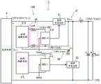
First, a schematic configuration of an insulated power supply and a power converter according to the present invention will be described with reference to fig. 1. The power conversion device shown in fig. 1 is an example of a configuration of a DCDC converter having a step-down chopper circuit as a main circuit.
The DCDC converter 10 is a main circuit including a step-down chopper circuit 12, and converts an input voltage Vin from the dc power supply 6 to output an output voltage Vout. The step-down chopper circuit 12 includes a series-parallel circuit of a high-side switching element S1 and a low-side switching element S2, and a series-parallel circuit of an inductor (inductance) L and a smoothing capacitor C, and supplies an output voltage Vout across the smoothing capacitor C to a load resistor R.
The high-side switching element S1 includes a high-side insulated power supply 2-H and a high-side driver circuit (gate driver) 3-H as a configuration for controlling the switching operation thereof. On the other hand, the low side includes a low side insulated power supply 2-L and a low side driver (gate driver) 3-L as a configuration for controlling the switching operation of the low side switching device S2. The reference voltage of the high-side insulated power supply 2-H and the reference voltage of the low-side insulated power supply 2-L are different and are insulated from each other.
On the low side, the low-side driver circuit (Gate driver) 3-L receives the drive voltage Vdrv-L2 from the low-side insulated power supply 2-L, and applies the drive voltage Vdrv-L2 to the Gate terminal of the low-side switching device S2 in accordance with the Gate signal Gate2 to drive the low-side switching device S2.
On the other hand, on the high side, the high side drive circuit (Gate driver) 3-H receives the supply of the drive voltage Vdrv-H2 from the high side insulated power supply 2-H, and applies the drive voltage Vdrv-H2 to the Gate terminal of the high side switching element S1 in accordance with the Gate signal Gate1 to drive the high side switching element S1. A common mode reactor (common mode reactor)4 is provided between the high-side insulated power supply 2-H and the high-side drive circuit (gate driver) 3-H on the high side.
When the high-side switching element S1 is turned on/off at a high frequency, a high-frequency displacement voltage Vs1-S is generated. The high-frequency offset voltage Vs1-S is applied as an offset voltage of the source side voltage to ground of the high-side switching element S1, overlapping the voltage VN, to an insulation transformer T-H (not shown in fig. 1) included in the high-side insulation power supply 2-H. By the high frequency displacement voltage Vs1-s, a slight leakage current flows in the parasitic capacitance CT-H of the insulation transformer T-H. The leakage current of the parasitic capacitance Ct-H of the insulation transformer T-H becomes a cause of malfunction of the high-side switching element S1.
The common mode reactor 4 provided on the high side receives a high-frequency displacement voltage Vs1-S generated by turning on/off the high-side switching element S1 at a high frequency, thereby preventing the parasitic capacitance Ct-H of the insulation transformer T-H of the high-side insulation power supply 2-H from being applied with the displacement voltage Vs1-S, reducing the leakage current, and suppressing the malfunction of the high-side switching element S1.
The leakage current flowing into the parasitic capacitance of the insulation transformer of the high-side insulation power supply by the high-frequency displacement voltage generated during the on/off operation of the high-side switching element is a common-mode current flowing in the same direction on the high-voltage wiring and the low-voltage wiring connecting the high-side insulation power supply and the high-side drive circuit. The common mode reactor 4 reduces the common mode current.
The common mode reactor 4 includes a plurality of systems. Fig. 1 (b), (c), and (d) show examples of the common mode reactor.
(common mode reactor)
The common mode reactor includes a common core and two coils wound in the same direction with respect to the common core. The common mode reactors 4A, 4B, and 4C shown in fig. 1 (B), (C), and (d) are configured by winding a high-voltage-side wire and a low-voltage-side wire of a high-side insulated power supply in the same direction with respect to a common core (not shown). The coil structure of the two conductive wires may be, for example, a split winding structure in which 2 conductive wires are separately wound around a core, or a double winding structure (parallel winding) in which two conductive wires are wound around a core in parallel.
Since the common mode current flows in the same direction to the high voltage side wiring and the low voltage side wiring of the high side insulated power supply, magnetic fluxes generated in the cores are combined to increase inductance by a mutual reinforcing self-induction action. Due to this increase in inductance, the electrical resistance against the high-frequency common mode current becomes high, and the effect of preventing the passage of the common mode current is generated. The effect of preventing the passage of the common mode current and the load of the displacement voltage Vs1-s by the common mode reactor prevent the parasitic capacitance of the insulation transformer from being applied with the displacement voltage, and suppress the leakage current flowing into the parasitic capacitance of the insulation transformer.
The common mode reactors 4A, 4B, and 4C are formed of iron cores independent of the inductance L of the main circuit such as a chopper circuit. By forming the cores (not shown) of the common mode reactors 4A, 4B, and 4C and the core (not shown) of the inductance L of the main circuit of the chopper circuit independently from each other, magnetic saturation of the cores of the common mode reactors 4A, 4B, and 4C due to the main current of the main circuit of the chopper circuit can be avoided. This makes it possible to reduce the size of the cores of the common mode reactors 4A, 4B, and 4C.
Further, by making the core of the common mode reactor and the core of the inductance L of the main circuit of the chopper circuit independent, the inductances of the respective cores can be determined separately, and by making the wire diameters of the coils wound around the cores of the common mode reactors 4A, 4B small and increasing the number of coils, the inductances can be set arbitrarily. Further, since the voltage-time product (Bm) can be set arbitrarily, magnetic saturation of the core can be suppressed.
The common mode reactor 4A is configured by winding primary coils 4A and 4b around a common core (not shown) in the same direction. The common mode reactor 4B includes a secondary coil 4c short-circuited with a resistor 4d, in addition to primary coils 4A and 4B wound around a common core in the same manner as the common mode reactor 4A. The secondary coil 4c induces a common mode current of the primary coils 4a and 4b, and is consumed by the resistor 4 d.
The common mode reactor 4C is wound around the primary coils 4A and 4b of the common core in the same manner as the common mode reactor 4A, and short-circuits the primary coils 4A and 4b with resistors 4e and 4 f. The resistors 4e and 4f consume the common mode current of the primary coils 4a and 4b to reduce the current.
On the other hand, only the low-side voltage VN is applied to the high-frequency offset voltage applied to the low-side isolation transformer T-L (not shown in fig. 1) of the low-side isolation power supply 2-L. When voltages VP and VN are set to high and low voltages obtained by grounding the neutral point of the Y-word line of the multiphase power supply, only a low frequency VN is applied to the parasitic capacitance Ct-L of the low-side insulation transformer T-L, and therefore only a small leakage current is present. When the frequency component of the voltage applied to low-side insulation transformer T-L is, for example, a 3-phase commercial power supply (50Hz) in which the input voltage neutral point is grounded, reference voltage VN has a frequency of 150Hz, and the leakage current of parasitic capacitance Ct-L of about several to several tens of pF can be almost ignored.
(bias power supply)
The low-side insulated power supply 2-L has the voltage VN as a reference voltage, and the high-side insulated power supply 2-H on the high side is in a floating state insulated from the low-side insulated power supply 2-L. The reference voltage of the high-side insulated power supplies 2-H is determined according to the voltage of the source terminal of the high-side switching element S1.
In the DCDC converter 10 of the power conversion device 1 of the present invention, the high-side insulated power supplies 2 to H include a bias power supply 5 connected to the low-voltage side. The bias power supply 5 adjusts a bias voltage of a high-frequency displacement voltage Vs1-s applied to the common mode reactor. By adjusting the bias voltage of the bias power supply 5, the core of the common mode reactor is magnetically reset, and magnetic saturation of the core is suppressed. The magnetic reset of the core by the bias power supply will be described in the following section.
(Voltage status of each part of the power converter)
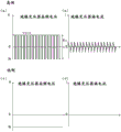
Next, the voltage state of each part of the power conversion device will be described with reference to fig. 2 and 3.
Fig. 2 shows a case where a 3-phase commercial power supply (50Hz) having a neutral point grounded and a rectifier and a smoothing circuit for rectifying an ac voltage of the 3-phase commercial power supply and outputting a dc voltage are used as a dc power supply, and the dc voltage obtained by the dc power supply is used as an input voltage Vin of the power conversion device. Fig. 2 (a) shows the variation of each voltage of the voltage VP at the positive voltage end, the voltage VN at the negative voltage end, and the voltage (VN + Vout) at the output end of the dc power supply, and fig. 2 (b) shows the variation of the high-frequency displacement voltage Vs1-s as the voltage of each part of the power conversion device. Fig. 2 (c) shows the voltage states of the voltages VP, VN + Vout, VN and Vs1-s at an arbitrary time point in fig. 2 (b).
The voltage VN at the negative voltage end, out of the voltages at the output end of the dc power supply, becomes the reference voltage at the low side of the power conversion device, and the voltage VP at the positive voltage end becomes a voltage (VN + Vin) obtained by adding the input voltage Vin to the reference voltage VN.
When the main circuit of the power conversion device is configured by a step-down chopper circuit, VP (VN + Vin) > (VN + Vout) has a relationship.
When the frequency of each commercial power supply is 50Hz, the output voltage of the dc power supply that rectifies the ac voltage of the 3-phase commercial power supply and outputs the dc voltage becomes 150Hz, and the frequency of the voltage VN and the voltage VP becomes 150 Hz. When S is grounded, the frequency of the voltage VN and the frequency of the voltage VP are 50 Hz.
The high-frequency shift voltage Vs1-S generated when the high-side switching device S1 and the low-side switching device S2 are driven at a high frequency has the same amplitude value as the input voltage Vin and is represented by a voltage state added based on the reference voltage VN.
Fig. 3 shows voltage states of the voltage VP (VN + Vin) at the positive voltage end with the voltage VN at the negative voltage end as the reference voltage, the output voltage (VN + Vout) at the output end, and the voltage (Vdrv-H + Vs1-S) of the gate driver signal that drives the gate of the high-side switching element S1. Since the voltage of the gate driver signal needs to be higher than the voltage on the output side (source side) of the high-side switching element S1, the reference voltage of the high-side insulated power supply 2-H is set to Vs1-S, and a voltage (Vdrv-H + VN + Vin) obtained by adding the voltage Vdrv-H to the reference voltage Vs1-S and taking the voltage (Vdrv-H + Vs1-S) as a peak voltage is set as the gate driver signal Vgate-H. The amplitude of the voltage shown in fig. 3 is schematically illustrated in the description, and does not indicate the actual amplitude of the voltage.
(magnetic reset)
In each mode of the common mode reactor, the bias power supply 5 magnetically resets the core of the common mode reactor, and suppresses magnetic saturation of the core of the common mode reactor.
The high-side switching element S1 turned on/off by the high-side insulated power supply 2-H generates a high-frequency offset voltage Vs1-S in accordance with the on/off operation. The high-frequency displacement voltage Vs1-s is applied to the common mode reactor. On the other hand, only a low-frequency voltage is applied to the parasitic capacitance Ct-H of the insulation transformer included in the high-side insulated power supply 2-H.
The reference potential of the high-side insulated power supply 2-H is in a floating state so as to be insulated from the low-side insulated power supply 2-L. Therefore, the high-frequency displacement voltage Vs1-s applied to the common mode reactor is superimposed on the reference potential in the floating state, and the magnetization state of the core of the common mode reactor, which fluctuates according to the displacement voltage Vs1-s, is controlled by the reference potential.
The bias power supply 5 adjusts the potential of the high-frequency displacement voltage Vs1-s with respect to the reference potential of the high-side insulated power supply 2-H, and magnetically resets the positive and negative voltage products of the core of the common mode reactor in a time-product balanced manner, thereby suppressing magnetic saturation of the core.
The bias voltage of the bias power supply 5 is an output voltage of an output circuit such as a chopper circuit driven by an insulated power supply, and thus the reference potential of the high-frequency offset voltage Vs1-s applied to the common mode reactor is adjusted in accordance with the output voltage. The common mode reactor is applied with voltage time products of opposite polarities and the same magnitude by adjusting the reference potential of the displacement voltage Vs1-s according to the bias power supply.
Fig. 4 is a schematic diagram for explaining potential adjustment based on the high-frequency displacement voltage Vs1-s of the bias power supply 5. The voltage amplitude and the voltage at each portion shown in fig. 4 are schematically shown in the description, and do not show the actual voltage amplitude and voltage state.
Fig. 4 (a) shows a potential state of a high-frequency displacement voltage Vs1-s applied to the common mode reactor. In the potential state shown in fig. 4 (a), the bias voltage is 1/2 of the input voltage Vin as an example, and the magnetic reset of the core is not performed because the voltage time product in the positive direction is applied to the common mode reactor in a large amount in the fluctuation of the displacement voltage Vs 1-s.
Fig. 4 (b) shows a state in which the high-frequency displacement voltage Vs1-s applied to the common mode reactor is changed in potential by the bias power supply in accordance with the reference voltage VN. According to this potential change, the reference potential of the common mode reactor becomes (VN + Vout). In fig. 4 (b), the (VN + Vout) is indicated by a thick dotted line.
Thus, a displacement voltage Vs1-s having the same area of voltage-time product is applied to the core of the common mode reactor in both the positive direction and the negative direction with respect to the reference potential (VN + Vout).
When the main circuit of the power conversion device is a step-down chopper circuit, the output voltage Vout of the step-down chopper circuit is represented by Vout — Vin × Duty. Duty is a Duty ratio of the high-side switching element S1, and represents a time ratio for turning on the high-side switching element S1 for one cycle.
When the drive of the high-side switching element S1 is controlled by the Duty, the voltage of (Vin-Vout) is applied to the common mode reactor only during the Duty while the high-side switching element S1 is in the on state, and the polarity of the voltage of Vout is applied to the common mode reactor in the reverse direction and only during the (1-Duty) while the high-side switching element S1 is in the off state.
When the voltage application state is represented by the voltage-time product Bm, the period during which the high-side switching element S1 is in the on state is
Bm-on=(Vin-Vout)×Duty
=(Vin-Vin×Duty)×Duty
=Vin×(1-Duty)×Duty…(1)
On the other hand, the high-side switching element S1 is in the off state
Bm-off=(-Vout×(1-Duty))
=-Vin×(1-Duty)×Duty…(2)
The displacement voltage Vs1-s is applied to the common mode reactor in its entirety, and the parasitic capacitance Ct-H of the insulation transformer T-H of the high-side insulated power supply 2-H is applied with only a low-frequency voltage of (VN + Vout).
As shown in the above equations (1) and (2), the displacement voltage Vs1-S applied to the common mode reactor has the voltage time product Bm-on applied to the core in the on state of the high-side switching element S1 and the voltage time product Bm-off applied to the core in the off state of the high-side switching element S1, which have opposite polarities and the same magnitude, and therefore the core of the common mode reactor is magnetically reset.
On the other hand, the parasitic capacitance Ct-H of the insulation transformer T-H is almost negligible for the leakage current due to the low-frequency voltage (VN + Vout) applied to the parasitic capacitance Ct-H, which is a small capacitance of several to several tens pF, for example.
(suppression of resonance phenomenon of high-side insulated Power supply)
Next, a configuration for suppressing a resonance phenomenon generated in the high-side insulated power supply will be described. When the coupling degree of the two coils 4A and 4B constituting the common mode reactors 4A and 4B is less than 1, a leakage inductance Ls (not shown in fig. 1) is generated. The leakage inductance Ls constitutes a resonance circuit together with the high-side insulated power supply 2-H and a capacitor provided in the drive circuit (gate driver) 3-H.
As capacitors constituting the resonance circuit, there are a smoothing capacitor provided in the high-side insulated power supply 2-H connected to the common mode reactors 4A and 4B, and a bypass capacitor (bypass capacitor) provided in the drive circuit (gate driver) 3-H. The bypass capacitor functions as a filter for bypassing the ac component and preventing the noise from partially entering the drive circuit (gate driver) 3-H.
In addition, since a capacitor having a large capacitance such as an electric field capacitor is generally used as a smoothing capacitor provided after rectification of the high-side insulated power supply, the capacitor can be ignored as a capacitor constituting the resonance circuit. In addition, in the case of using a photocoupler for insulation in the drive circuit (gate driver), the bypass capacitor provided in the drive circuit is a small capacitor having a capacitance such as a ceramic capacitor, and therefore cannot be ignored as a capacitor constituting the resonant circuit.
The common mode reactors 4A and 4B may be configured such that a damping resistance (damping resistance)7 (not shown in fig. 1) is connected in series to both the high-voltage-side wiring and the low-voltage-side wiring of the high-side insulated power supply 2-H. The damping resistor 7 damps resonance by damping a resonance current generated by a resonance phenomenon between a capacitor and leakage inductances Ls of the two coils 4A and 4B constituting the common mode reactors 4A and 4B.
In the series circuit of the leakage inductance Ls, the capacitor C, and the damping resistance Rdamp, the Q value and the damping ratio ζ are expressed by the following expressions (3) and (4), respectively.
Q=(1/R damp)×(Ls/C)1/2…(3)
ζ=1/2Q=(R damp/2)×(C/Ls)1/2…(4)
Here, the damping resistance Rdamp can be selected by, for example, obtaining a value at which the damping ratio ζ exceeds a predetermined value.
Here, when the smoothing capacitor does not contribute to resonance, and the capacitor constituting the resonance circuit is simply a bypass capacitor Cs-in for bypassing the photocoupler of the drive circuit (gate driver), the attenuation ratio ζ is expressed by the following equation (5).
ζ=1/2Q=(R damp/2)×(Cs-in/Ls)1/2…(5)
When ζ k is determined as a predetermined value of the attenuation value ζ, the damping resistance Rdamp can be expressed by the following equation (6).
R damp>2ζk×(Ls/Cs-in)1/2…(6)
Hereinafter, configuration examples (1 st configuration example to 6 th configuration example) of the insulated power supply and the power conversion device according to the present invention will be described with reference to fig. 5 to 12. The 1 st to 3 rd configuration examples shown in fig. 5 to 9 are mode examples of the bias power supply, and show an example of a DCDC converter having a step-down chopper circuit as a main circuit. The 4 th configuration example shown in fig. 10 is an example of a DCDC converter having a boost chopper circuit as a main circuit, the 5 th configuration example shown in fig. 11 is an example of an interleaved configuration of the DCDC converter, and the 6 th configuration example shown in fig. 12 is an example of a configuration of a DCAC inverter.
(embodiment 1)
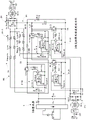
In configuration example 1, the bias power supply 5A according to configuration example 1 applies a voltage to the high-side insulated power supply. Fig. 5 shows an outline module, and fig. 6 shows an example of the configuration.
A DCDC converter 10A of configuration example 1 includes a bias power supply 5A of configuration example 1 as a bias power supply of the configuration shown in fig. 1. The bias power supply 5A is configured to connect the high output terminal of the step-down chopper circuit 12 to the low voltage side of the high-side insulated power supplies 2 to H, and by this configuration, the voltage (VN + Vout) of the output terminal on the high voltage side of the step-down chopper circuit 12 is applied to the low voltage side of the high-side insulated power supplies 2 to H, thereby setting the reference potential of the high-side insulated power supplies 2 to H.
The voltage (VN + Vout) at the high-voltage-side output terminal of the step-down chopper circuit 12 is a voltage obtained by superimposing the voltage VN at the negative-voltage-side output terminal of the step-down chopper circuit 12 on the output voltage Vout applied to the load resistor R.
Fig. 6 shows a circuit configuration of the summary module shown in fig. 5.
The dc power supply 6 includes a 3-phase power supply with a grounded neutral point, a 3-phase rectifier for converting 3-phase ac into dc, and a smoothing circuit including a series-parallel circuit of a coil Lin and a capacitor Cin. For example, a 3-phase commercial power supply of 50Hz may be used as the 3-phase power supply. When a 3-phase commercial power supply of 50Hz is used, the frequency of reference voltage VN obtained by dc power supply 6 is 150 Hz.
The high side insulation power supply 2-H is configured by connecting a high side dc power supply, a high side inverter INV-H for dc-ac converting the dc voltage Vdrv-H1 of the high side dc power supply, a high side insulation transformer T-H for voltage converting the ac output of the high side inverter INV-H, a high side rectifier RECT-H for converting the ac output of the high side insulation transformer T-H into dc in series, and a smoothing capacitor Cs-Hout in parallel.
The high-side drive circuit 3-H includes a high-side gate driver DRV-H for controlling the on/off operation of the high-side switching element S1, a high-side optical switch (photo switch) PC-H for controlling the drive of the high-side gate driver DRV-H, and a high-side bypass capacitor Cs-Hin for removing noise input to the high-side optical switch PC-H, which are connected in series. The output of the high-side gate driver DRV-H is input to the gate of the high-side switching element S1 via a resistor Rg-H.
The low-side insulation power supply 2-L is configured by connecting a low-side dc power supply, a low-side inverter INV-L for dc-ac converting a dc voltage Vdrv-L1 of the low-side dc power supply, a low-side insulation transformer T-L for voltage converting an ac output of the low-side inverter INV-L, and a low-side rectifier RECT-L for converting an ac output of the low-side insulation transformer T-L into a dc voltage in series, and connecting a smoothing capacitor Cs-Lout in parallel.
The low-side driver circuit 3-L is provided with: a low-side gate driver DRV-L for controlling the ON/OFF operation of the low-side switching device S2, a low-side optical switch PC-L for performing drive control of the low-side gate driver DRV-L, and a low-side bypass capacitor Cs-Lin for removing noise input to the low-side optical switch PC-L. The output of the low side gate driver DRV-L is input to the gate of the low side switching device S2 via resistor Rg-L.
A common mode reactor 4A is provided on a wiring between the high-side insulated power supply 2-H and the high-side drive circuit 3-H. The common mode reactor 4A is formed by a coil Lcom connected to both high-voltage-side wiring and low-voltage-side wiring connected between the smoothing capacitor Cs-Hout on the high-side insulated power supply 2-H side and the high-side bypass capacitor Cs-Hin on the high-side drive circuit 3-H side.
In addition, an inductance Ls in fig. 6 indicates a leakage inductance of the common mode reactor 4A, and Rdamp is a damping resistance that suppresses resonance generated by the leakage inductance Ls.
(embodiment 2)
Configuration example 2 applies a voltage to the high-side insulated power supply by the bias power supply of the 2 nd aspect.
Fig. 7 shows an outline module, and fig. 8 shows an example of the configuration.
A DCDC converter 10B of configuration example 2 includes a bias power supply 5B of embodiment 2 as a bias power supply of the configuration shown in fig. 1. The bias power supply 5B is configured to apply a low voltage to the high-side insulated power supplies 2 to H by another power supply, and the voltage source Vc of the other power supply is set to the same voltage as the voltage (VN + Vout) obtained by adding the output voltage Vout to the voltage VN at the negative voltage end of the step-down chopper circuit. With this configuration, the same voltage as the voltage (VN + Vout) at the high output terminal of the step-down chopper circuit 12 is set as the potential on the low voltage side of the high-side insulated power supply 2-H.
Fig. 8 shows a circuit configuration of the summary module shown in fig. 7. The circuit configuration shown in fig. 8 is the same except that the bias power supply 5A of the circuit configuration shown in fig. 6 is changed to the bias power supply 5B. Hereinafter, the description of the portions common to the 1 st configuration example shown in fig. 6 will be omitted, and only the bias power supply 5B will be described.
The bias power supply 5B is configured by connecting a voltage source Vc to the low voltage side of the high side isolation power supplies 2 to H. The voltage source Vc is set to the same voltage as the output voltage Vout of the main circuit. Thus, the voltage of (VN + Vout) is set on the low voltage side of the high-side insulated power supply 2-H. When the input voltage of the step-down chopper circuit 12 as the main circuit is Vin and the Duty ratio of the high-side switching element S1 is Duty, the voltage of the voltage source Vc is set to (Vin × Duty). Therefore, the voltage of the voltage source Vc of the bias power supply 5B can be set according to the known input voltages Vin and Duty.
(configuration example 3)
Configuration example 3 applies a voltage to the high-side insulated power supply by the bias power supply of the 3 rd embodiment.
Fig. 9 shows a schematic block diagram.
A DCDC converter 10C of configuration example 3 includes a bias power supply 5C of embodiment 3 as a bias power supply of the configuration shown in fig. 1. The bias power supply 5C sets the potential on the low voltage side of the high-side isolation power supply 2-H by another power supply, and the voltage source Vc of the other power supply generates the same voltage as the output voltage Vout from the Gate signals Gate1 and Gate2, as in the bias power supply 5B of the 2 nd embodiment. With this configuration, the voltage (VN + Vout) at the high output terminal of the step-down chopper circuit 12 is set as the potential on the low voltage side of the high-side insulated power supply 2-H.
The bias power supply 5C is configured by connecting the bias power supply 5C between the low voltage side of the main circuit of the step-down chopper circuit and the low voltage side of the high-side insulated power supplies 2 to H. The bias power supply 5C includes a bias power supply circuit 5C1 and a controller 5C 2. The control unit 5C2 receives the Gate signal Gate1 for controlling the high-side driver circuit 3-H to be turned on/off, the Gate signal Gate2 for controlling the low-side driver circuit 3-L to be turned on/off, and the input voltage Vin, calculates the Duty ratio Duty from the Gate signal Gate1 and the Gate signal Gate2, and generates the same voltage as the output voltage Vout by an operation (Vin × Duty) based on the acquired Duty and the input voltage Vin. Thus, the bias power supply 5C can constitute a voltage source Vc that outputs the same voltage as the output voltage Vout of the main circuit, and the voltage of (VN + Vout) is set at the potential on the low voltage side of the high-side insulated power supply 2-H.
With the configuration of the bias power supply 5C, the Gate signals Gate1 and Gate2 and the voltage synchronized with the fluctuation of the input voltage Vin can be set in the high-side insulated power supply 2-H.
(configuration example 4)
The 4 th configuration example is an example in which a DCDC converter is configured using a step-up chopper circuit instead of a step-down chopper circuit as a main circuit of a power conversion device. Fig. 10 (a) shows a schematic block diagram, and fig. 10 (b) shows a voltage relationship between the respective portions.
The DCDC converter 10D of the configuration example 4 includes a boost chopper circuit 13 as a main circuit of the power conversion device. The DCDC converter 10D has a boost chopper circuit 13 as a main circuit, converts an input voltage Vin from the dc power supply 6, and outputs a boosted voltage Vout. The boost chopper circuit 13 includes a series-parallel circuit including a high-side switching element S1 and a low-side switching element S2 between an inductor L and a smoothing capacitor C constituting the series-parallel circuit, and supplies an output voltage Vout to a load resistor R.
In configuration example 4, the configuration of the high side including the high-side insulated power supply 2-H, the high-side driver circuit 3-H, and the common mode reactor 4, and the configuration of the low side including the low-side insulated power supply 2-L and the low-side driver circuit 3-L are the same as those in configuration examples 1 to 3 including the step-down chopper circuit, and therefore, descriptions of these configurations are omitted.
A DCDC converter 10D of the 4 th configuration example includes a bias power supply 5D of the 4 th aspect. The bias power supply 5D is configured such that the input terminal on the low voltage side, which is the boost chopper circuit 13, is connected to the low voltage side of the high-side insulated power supplies 2 to H. With this configuration, the voltage (VN + Vin) at the low input terminal of the boost chopper circuit 13 is set as the potential on the low voltage side of the high-side insulated power supplies 2 to H.
Fig. 10 (b) shows the voltage states of the positive voltage VP at the input end of the main circuit (VN + Vin), the output voltage at the output end of the main circuit (VN + Vout), and the voltage of the gate driver signal (Vdrv-H + VN + Vout) that drives the gate of the high-side switching element S1, with the voltage VN at the negative voltage end of the main circuit as the reference voltage.
Since the voltage of the gate driver signal needs to be higher than the voltage on the output side (source side) of the high-side switching element S1, the reference voltage of the high-side insulated power supply 2-H is set to Vs1-S, and a voltage (Vdrv-H + VN + Vout) obtained by adding the voltage Vdrv-H to the reference voltage Vs1-S is regarded as a peak voltage (Vdrv-H + Vs1-S) as the gate driver signal Vgate-H. The amplitude of the voltage shown in fig. 10 (b) is schematically illustrated in the description, and does not indicate the actual amplitude of the voltage.
(example of the 5 th configuration)
The 5 th configuration example is an example in which the main circuit of the power conversion device is configured by a multi-phase configuration by interleaving. Here, a step-down chopper circuit is used as a main circuit, and an example of a DCDC converter having a configuration of 2-phase interleaving is shown. Fig. 11 shows a circuit example of the 5 th configuration example.
The DCDC converter 10E of the configuration example 5 constitutes a main circuit in 2 phases by interleaving of the power conversion device.
In this multiphase configuration, the same number of common mode reactors as the number of interleaved phases are provided on the high side of each phase. The high-side insulated power supplies 2 to H and the low-side insulated power supplies 2 to L may be 1 insulated power supply in common for each phase.
In the configuration example shown in FIG. 11, 2 common mode reactors 4A-A and 4A-B and 2 high side drive circuits 3-HA and 3-HB are provided for 1 high side insulated power supply 2-H on the high side, one phase is constituted by the common mode reactor 4A-A and the high side drive circuit 3-HA, and the other phase is constituted by the common mode reactor 4A-B and the high side drive circuit 3-HB.
On the other hand, 2 low-side driver circuits 3-LA and 3-LB are provided for 1 low-side insulated power supply 2-L on the low side, and one phase is configured by low-side driver circuit 3-LA and the other phase is configured by low-side driver circuit 3-LB.
In the power converter having the interleave structure, when the same values as those of the coil Lcom and the damping resistance Rdamp of the common mode reactor set in the single-phase power converter shown in the configuration example 1 are selected, the voltage Vdrv-H2-a applied to the high-side bypass capacitor Cs-Hin-a of the optocoupler of the high-side drive circuit 3-HA and the voltage Vdrv-H2-B applied to the high-side bypass capacitor Cs-Hin-B of the optocoupler of the high-side drive circuit 3-HB become the same voltages. This voltage is a gate voltage applied to the gate of the high-side switching element S1-A, S1-B, and affects the on-resistance of the switching element, but according to the present configuration, the gate voltages applied to the gates of both switching elements are the same voltage, so that the currents flowing into the phases of the main circuit that are woven at most can be made the same current value, and imbalance of the currents can be prevented.
Although 2-phase interleaving is shown as an example of polyphase interleaving, the number of interleaved phases is not limited to 2, and the same applies to multi-phase interleaving of 3 or more phases.
In the DCDC converter 10E of the configuration example 5, the DCDC step-down chopper converter is shown as the main circuit, but the same is applicable to a converter in which the main circuit is a DCDC step-up chopper converter.
In these multiphase interleaving, the high-side and low-side of the converter may each have a multiphase configuration with respect to a common single isolated power supply, and in this multiphase configuration, the high-side multiphase configuration includes a plurality of high-side switching elements connected in parallel. These plurality of high-side switching elements are applied with the same voltage from a common insulated power supply on the high side via a common mode reactor. By setting the voltages applied to the high-side switching elements to the same voltage, the on-resistances of the high-side switching elements can be made uniform, and the outputs of the phases can be equalized.
(example 6 construction)
The 6 th configuration example is an example in which the power conversion device is configured as a DCAC inverter, and performs power conversion on a dc input voltage Vin to output an ac output voltage Vout to an output impedance (impedance) RL. In the configuration example of the DCAC inverter 11 shown in fig. 12, a bridge circuit is configured by 2 high-side driver circuits 3-HA and 3-HB on the high side and 2 low-side driver circuits 3-LA and 3-LB on the low side. A voltage is supplied to 2 high-side drive circuits 3-HA and 3HB from 1 common high-side insulated power supply 2-H. In addition, voltage is supplied to 2 low-side driver circuits 3-LA and 3-LB from 1 common low-side insulated power supply 2-L.
Further, on the high side, a common mode reactor 4A is connected between the high side insulated power supply 2-H and the high side drive circuit 3-HA, and a common mode reactor 4B is connected between the high side insulated power supply 2-H and the high side drive circuit 3-HB.
A bias power supply Vc is connected between the low voltage side of the high side insulated power supply 2-H and the low voltage side of the main circuit, and the voltage on the low voltage side of the high side insulated power supply 2-H is set to (VN + Vc). On the other hand, the low-voltage side of the low-side insulated power supply 2-L and the low-voltage side of the main circuit are connected, and the reference voltage of the low-side insulated power supply 2-L is set to VN.
Here, the voltage of the bias power source Vc is selected to be (Vin/2). In each cycle, since the high-side driver circuits 3-HA and 3-HB constituting the bridge circuit receive a voltage of 1/2 of the input voltage Vin, the bias power source Vc is selected to be (Vin/2), and the common mode reactors 4A and 4B can be appropriately magnetically reset.
In addition, the values of the inductance Lcom-a and the inductance Lcom-B of the common mode reactors 4A and 4B are selected to be sufficiently large values with respect to the output impedance RL of the DCAC inverter 11, whereby the impedance of the high-side insulated power supply 2-H as viewed from the DCAC inverter 1 can be set sufficiently larger than the output impedance of the DCAC inverter 11 in the high frequency band. This can reduce the influence of the high-side insulated power supplies 2 to H on the output impedance viewed from the DCAC inverter 11. This effect is because the core of the common mode reactor is separated and independent from the core of the main circuit, and the inductance of the common mode reactor can be freely set.
In the DCAC inverter system shown in configuration example 6, the bridge circuit includes a plurality of switching elements S1-A, S1-B, S2-A, S2-B connected in parallel to a common isolated power supply on the high side and the low side, respectively. These high-side switching elements S1-A, S1-B are supplied with the same voltage from a common one of the high-side insulated power supplies 2-H via the common mode reactors 4A, 4B. By setting the voltages applied to the high-side switching devices S1 to A, S1-B to the same voltage, the on-resistances of the high-side switching devices S1 to A, S1-B can be made uniform, and variations in the output voltage of the DCAC inverter can be suppressed.
The above embodiments and modifications are described as examples of the power supply device according to the present invention, and the present invention is not limited to the embodiments, and various modifications can be made according to the gist of the present invention, and these are not excluded from the scope of the present invention.
Industrial applicability
The power conversion device of the present invention can be applied to supplying high-frequency power to a device using high frequency, such as a manufacturing device for a semiconductor or a liquid crystal panel, a vacuum deposition device, or a heating and melting device.
Description of the symbols
1: power conversion device
2-H: high side insulation power supply
2-L: low side isolated power supply
3-H, 3-HA, 3-HB: high-side driving circuit
3-L, 3-LA, 3-LB: low side driver circuit
4. 4A, 4B, 4C, 4A-A, 4A-B: common mode reactor
4a, 4b, 4 c: coil
4 d: resistance (RC)
4e, 4 f: capacitor with a capacitor element
5. 5A, 5B, 5C, 5D: bias power supply
5C 1: bias power supply circuit
5C 2: control unit
6: direct current power supply
7: damping resistor
10. 10A, 10B, 10C, 10D, 10E: DCDC converter
11: DCAC inverter
12: voltage-reducing chopper circuit
13: boost chopper circuit
100: direct current power supply
110: DCDC converter power supply
120H: high side insulation power supply
120L: low side isolated power supply
130H, 130L: gate driver
C: smoothing capacitor
Cin: capacitor with a capacitor element
Cs-in: bypass capacitor
Cs-Hin, Cs-Hin-A, Cs-Hin-B: high side bypass capacitor
Cs-Hout, Cs-Lout: smoothing capacitor
Cs-Lin: low side bypass capacitor
Ct-H, Ct-L: parasitic capacitance
DRV-H: high side gate driver
DRV-L: low side gate driver
GateH, GateL, Gate1, Gate 2: grid signal
INV-H: high side converter
INV-L: low-side inverter
L, Lcom-A, Lcom-B, Ls: inductance
Lcom, Lin: coil
PC: optical switch
PC-H: high side light switch
PC-L: low side light switch
R: load resistance
RG-H: driving resistor
RG-L: driving resistor
Rdamp: damping resistor
Rg-H, Rg-L: resistance (RC)
RECT-H: high side rectifier
RECT-L: low-side rectifier
RL: output impedance
S1, S1-A, S1-B: high side switch element
S2: low-side switching element
T-H: high side insulation transformer
T-L: low-side insulation transformer
Vdrv-H1, Vdrv-L1: direct voltage
Vdrv-H1, Vdrv-L2: DC voltage (driving voltage)
Vgate-H: gate driver signal
VN: reference voltage
VP: reference voltage
Vc: voltage source, bias power supply
Vin: input voltage
Vout: output voltage
Vs 1-s: the displacement voltage.
Claims (14)
1. An insulated power supply is provided with: a high-side insulated power supply for supplying a driving voltage to a high-side driving circuit for controlling the switching operation of the high-side switching element via an insulation transformer; and a low-side insulated power supply for supplying a driving voltage to a low-side driving circuit for controlling the switching operation of the low-side switching device via an insulation transformer,
a bias power supply connected to a low voltage side of the high side insulation power supply and setting a reference potential of the high side insulation power supply,
the bias voltage of the bias power supply is an output voltage of an output circuit driven by the high-side driver circuit,
the high-side insulated power supply includes a common mode reactor between the insulation transformer and the high-side drive circuit,
the common mode reactor is provided on two lines, i.e., a high-voltage line and a low-voltage line, connecting the insulation transformer and a high-side bypass capacitor of the high-side drive circuit, reduces common mode currents flowing in the same direction on the two lines, and suppresses leakage currents flowing in a parasitic capacitance of the insulation transformer,
the common mode reactor is loaded with a high-frequency displacement voltage generated by a high-frequency operation of the high-side switching element,
the bias power supply adjusts the potential of the high-frequency displacement voltage with respect to the reference potential of the high-side insulated power supply, and magnetically resets the core of the common mode reactor by balancing the voltage-time product in the positive direction and the negative direction.
2. The isolated power supply of claim 1,
the high-side insulated power supply includes, connected in series: a high-side DC power supply, a high-side inverter for DC-AC converting the DC voltage of the high-side DC power supply, a high-side insulation transformer for voltage converting the AC output of the high-side inverter, and a high-side rectifier for converting the AC output of the high-side insulation transformer into DC,
the high-side drive circuit includes a high-side gate driver for controlling an ON/OFF operation of the high-side switching element and a high-side optical switch for controlling a drive of the high-side gate driver, which are connected in series, and a high-side bypass capacitor for removing a noise input to the high-side optical switch, which is connected in parallel between a high-side voltage side and a low-side voltage side of the high-side gate driver,
the low-side insulated power supply is provided with: a low-side DC power supply, a low-side inverter for DC-AC converting the DC voltage of the low-side DC power supply, a low-side insulation transformer for voltage converting the AC output of the low-side inverter, and a low-side rectifier for converting the AC output of the low-side insulation transformer into DC,
the low-side driver circuit includes a low-side gate driver for controlling an on/off operation of the low-side switching device and a low-side optical switch for controlling driving of the low-side gate driver, which are connected in series, and a low-side bypass capacitor for removing noise input to the low-side optical switch, which is connected in parallel between a high-voltage side and a low-voltage side of the low-side driver circuit.
3. The isolated power supply of claim 1 or 2,
the common mode reactor winds the high-voltage-side wiring and the low-voltage-side wiring of the high-side insulated power supply in the same direction with respect to the common core.
4. The isolated power supply of claim 3,
the insulated power supply includes a damping resistor connected in series to the common mode reactor.
5. The isolated power supply of claim 3,
the common core of the common mode reactor and the core of the coil provided in the circuit driven and controlled by the high-side driver circuit and the low-side driver circuit are separated and independent from each other.
6. The isolated power supply of claim 1,
the bias voltage of the bias power supply is an output voltage of the output circuit driven by the high-side driver circuit.
7. A power conversion device constituting a DCDC converter, the power conversion device comprising: a step-down chopper circuit configured by connecting a series-parallel connection circuit in which a high-side switching element and a low-side switching element are connected in series to a direct-current power supply, and an inductor; and
the isolated power supply of any of the above claims 1 to 6,
it is characterized in that the preparation method is characterized in that,
the insulated power supply is a power supply that drives a high-side driver circuit and a low-side driver circuit, wherein the high-side driver circuit and the low-side driver circuit drive the high-side switching device and the low-side switching device.
8. The power conversion device according to claim 7,
the bias voltage of the bias power supply is the output voltage of the step-down chopper circuit.
9. A power conversion device constituting a DCDC converter, the power conversion device comprising: a boost chopper circuit configured by connecting a direct-current power supply in series with a inductor and a series-parallel connection circuit of a high-side switching element and a low-side switching element; and
the isolated power supply of any of the above claims 1 to 6,
it is characterized in that the preparation method is characterized in that,
the insulated power supply is a power supply that drives a high-side driver circuit and a low-side driver circuit, wherein the high-side driver circuit and the low-side driver circuit drive the high-side switching device and the low-side switching device.
10. The power conversion device according to claim 9,
the bias voltage of the bias power supply is the input voltage of the boost chopper circuit.
11. The power conversion device according to any one of claims 7 to 10,
the high side and the low side are each constituted by a plurality of phases by interleaving with respect to a common insulated power supply,
the high-side multiphase structure includes a plurality of high-side switching elements connected in parallel, and the voltage applied to the plurality of high-side switching elements is the same voltage supplied from the common high-side insulated power supply via the common mode reactor.
12. A power converter which constitutes a DCAC inverter including a bridge circuit including a high-side switching element and a low-side switching element for a direct-current power source,
the power conversion device includes the insulated power supply according to any one of claims 1 to 6,
the high-side driver circuit and the low-side driver circuit of the insulated power supply drive the high-side switching device and the low-side switching device.
13. The power conversion device according to claim 12,
the insulated power supply includes a bias power supply connected to a low-voltage side of the high-side insulated power supply, and a bias voltage of the bias power supply is 1/2 of an input voltage of the DCAC inverter.
14. The power conversion device according to claim 12 or 13,
the bridge circuit includes a plurality of switching elements connected in parallel to a common insulated power supply on the high side and the low side,
the voltage applied to the plurality of high-side switching elements is the same voltage supplied from the common one of the high-side insulated power supplies via the common mode reactor.
Applications Claiming Priority (3)
| Application Number | Priority Date | Filing Date | Title |
|---|---|---|---|
| JP2017019865A JP6784607B2 (en) | 2017-02-06 | 2017-02-06 | Insulated power supply and power converter |
| JP2017-019865 | 2017-02-06 | ||
| PCT/JP2017/006754 WO2018142631A1 (en) | 2017-02-06 | 2017-02-23 | Insulated power source and power conversion device |
Publications (2)
| Publication Number | Publication Date |
|---|---|
| CN110268613A CN110268613A (en) | 2019-09-20 |
| CN110268613B true CN110268613B (en) | 2021-12-31 |
Family
ID=63039484
Family Applications (1)
| Application Number | Title | Priority Date | Filing Date |
|---|---|---|---|
| CN201780085653.6A Active CN110268613B (en) | 2017-02-06 | 2017-02-23 | Insulated power supply and power conversion device |
Country Status (8)
| Country | Link |
|---|---|
| US (1) | US10992217B2 (en) |
| EP (1) | EP3550704B1 (en) |
| JP (1) | JP6784607B2 (en) |
| KR (1) | KR102294894B1 (en) |
| CN (1) | CN110268613B (en) |
| PL (1) | PL3550704T3 (en) |
| TW (1) | TWI731953B (en) |
| WO (1) | WO2018142631A1 (en) |
Families Citing this family (11)
| Publication number | Priority date | Publication date | Assignee | Title |
|---|---|---|---|---|
| GB2565297B (en) * | 2017-08-07 | 2020-09-02 | Murata Manufacturing Co | An adjustable power supply device for supplying power to a power switch control device |
| KR102542941B1 (en) * | 2018-06-08 | 2023-06-14 | 현대자동차주식회사 | Charging apparatus capable of reducing low frequency leakage current |
| US11228238B2 (en) | 2018-12-12 | 2022-01-18 | Hyundai Motor Company | Charging apparatus capable of reducing low-frequency leakage current |
| US11018519B2 (en) | 2018-12-12 | 2021-05-25 | Hyundai Motor Company | Charging apparatus capable of reducing low frequency leakage current |
| US20200412362A1 (en) * | 2019-06-25 | 2020-12-31 | Enersys Delaware Inc. | Electrical power switching circuits |
| JP2021164289A (en) | 2020-03-31 | 2021-10-11 | 株式会社京三製作所 | Driver device for class D full bridge amplifier |
| EP4122099A4 (en) * | 2020-04-17 | 2024-04-10 | Murata Manufacturing Co | Isolated gate driver |
| CN112491252A (en) * | 2020-12-30 | 2021-03-12 | 深圳市永联科技股份有限公司 | Driving method and circuit for improving reliability of SIC MOSFET |
| EP4037187A1 (en) * | 2021-01-29 | 2022-08-03 | ABB Schweiz AG | Semiconductor unit with asymmetrically arranged common mode chokes on gate driver input side |
| CN113391170B (en) * | 2021-05-26 | 2022-10-18 | 上海电力大学 | Method for monitoring end insulation state of inverter driving motor on line |
| US20230268858A1 (en) * | 2022-02-23 | 2023-08-24 | Hamilton Sundstrand Corporation | Parasitic immune isolated drive |
Citations (2)
| Publication number | Priority date | Publication date | Assignee | Title |
|---|---|---|---|---|
| CN1468463A (en) * | 2001-02-06 | 2004-01-14 | �������ʹ�ҵ����˾ | Half-bridge gate driver circuit |
| CN102684461A (en) * | 2011-03-15 | 2012-09-19 | 英飞凌科技股份有限公司 | Semiconductor device including circuit to compensate for parasitic inductance |
Family Cites Families (10)
| Publication number | Priority date | Publication date | Assignee | Title |
|---|---|---|---|---|
| JPH0833315A (en) * | 1994-07-08 | 1996-02-02 | Toshiba Corp | Load driver |
| US7068005B2 (en) * | 2004-08-30 | 2006-06-27 | Hamilton Sundstrand Corporation | Motor drive with damper |
| JP4458353B2 (en) | 2004-12-28 | 2010-04-28 | 株式会社タムラ製作所 | High side drive circuit |
| FR2915031B1 (en) * | 2007-04-16 | 2009-05-22 | Renault Sas | ELECTRIC ENERGY EXCHANGE SYSTEM, ESPECIALLY FOR A HYBRID VEHICLE. |
| JP2010119177A (en) * | 2008-11-12 | 2010-05-27 | Rohm Co Ltd | Multiphase dc/dc converter |
| US8324875B2 (en) | 2008-10-30 | 2012-12-04 | Rohm Co., Ltd. | Multiphase DC/DC converter with output phases deviated from or aligned with each other and driven with fixed on time |
| DE102008055157A1 (en) | 2008-12-23 | 2010-06-24 | Infineon Technologies Ag | Control circuit for a power semiconductor device and power semiconductor device |
| JP5243347B2 (en) * | 2009-06-05 | 2013-07-24 | 三菱電機株式会社 | High frequency AC power supply |
| US9866102B2 (en) | 2014-12-03 | 2018-01-09 | Nissan Motor Co., Ltd. | Power conversion device |
| JP6370279B2 (en) * | 2015-09-09 | 2018-08-08 | 三菱電機株式会社 | Bootstrap compensation circuit and power module |
-
2017
- 2017-02-06 JP JP2017019865A patent/JP6784607B2/en active Active
- 2017-02-23 US US16/475,180 patent/US10992217B2/en active Active
- 2017-02-23 WO PCT/JP2017/006754 patent/WO2018142631A1/en unknown
- 2017-02-23 CN CN201780085653.6A patent/CN110268613B/en active Active
- 2017-02-23 PL PL17894958T patent/PL3550704T3/en unknown
- 2017-02-23 KR KR1020197017436A patent/KR102294894B1/en active IP Right Grant
- 2017-02-23 EP EP17894958.2A patent/EP3550704B1/en active Active
- 2017-03-28 TW TW106110349A patent/TWI731953B/en active
Patent Citations (2)
| Publication number | Priority date | Publication date | Assignee | Title |
|---|---|---|---|---|
| CN1468463A (en) * | 2001-02-06 | 2004-01-14 | �������ʹ�ҵ����˾ | Half-bridge gate driver circuit |
| CN102684461A (en) * | 2011-03-15 | 2012-09-19 | 英飞凌科技股份有限公司 | Semiconductor device including circuit to compensate for parasitic inductance |
Also Published As
| Publication number | Publication date |
|---|---|
| CN110268613A (en) | 2019-09-20 |
| EP3550704A4 (en) | 2020-07-15 |
| US20190341847A1 (en) | 2019-11-07 |
| JP6784607B2 (en) | 2020-11-11 |
| JP2018129891A (en) | 2018-08-16 |
| TW201830842A (en) | 2018-08-16 |
| PL3550704T3 (en) | 2022-05-30 |
| TWI731953B (en) | 2021-07-01 |
| EP3550704A1 (en) | 2019-10-09 |
| EP3550704B1 (en) | 2022-03-30 |
| WO2018142631A1 (en) | 2018-08-09 |
| US10992217B2 (en) | 2021-04-27 |
| KR20190080944A (en) | 2019-07-08 |
| KR102294894B1 (en) | 2021-08-26 |
Similar Documents
| Publication | Publication Date | Title |
|---|---|---|
| CN110268613B (en) | Insulated power supply and power conversion device | |
| CN110289777B (en) | Three-phase soft switching PFC rectifier | |
| JP4910078B1 (en) | DC / DC converter and AC / DC converter | |
| US7463498B1 (en) | Apparatus for isolated switching power supply with coupled output inductors | |
| JP3656865B2 (en) | converter | |
| JP6511224B2 (en) | Power supply | |
| TWI536709B (en) | Power systme and method for providing power | |
| US20080247195A1 (en) | Dc/dc converter | |
| US20150188437A1 (en) | Power supply apparatus, power supply system with the power supply apparatus, and method of controlling the same | |
| US11296607B2 (en) | DC-DC converter | |
| JPH07250471A (en) | Three-phase sine-wave input switching power circuit | |
| CN109274273A (en) | Multiple Output Flyback Converter, motor driver and new-energy automobile | |
| JP4124814B2 (en) | Input / output isolated DC-DC converter | |
| US5995398A (en) | Power supply device | |
| JP6045664B1 (en) | Power converter | |
| GB2346744A (en) | Heavy duty isolating converter | |
| CN207459985U (en) | For the circuit being filtered to the signal from power supply | |
| JP2009165337A (en) | Power supplying device | |
| US9923480B2 (en) | DC-to-AC power converter with high efficiency | |
| US20180198382A1 (en) | Passive boost network and dc-dc boost converter applying the same | |
| US11863085B2 (en) | Converter assembly | |
| JPH09131056A (en) | Power-factor improved converter circuit | |
| WO2023122105A1 (en) | Transformerless bidirectional dc charger for electric vehicles | |
| CN113808818A (en) | Electric reactor |
Legal Events
| Date | Code | Title | Description |
|---|---|---|---|
| PB01 | Publication | ||
| PB01 | Publication | ||
| SE01 | Entry into force of request for substantive examination | ||
| SE01 | Entry into force of request for substantive examination | ||
| GR01 | Patent grant | ||
| GR01 | Patent grant |