Disclosure of Invention
The array substrate provided by the embodiment of the invention comprises a substrate, a first electrode and a second electrode which are positioned on the substrate, wherein the first electrode and the second electrode are configured to generate an electric field parallel to the upper surface of the substrate, the upper surface is the surface of the substrate facing the first electrode and the second electrode, the array substrate further comprises a quantum rod orientation layer and a quantum rod layer positioned on the quantum rod orientation layer, and quantum rods in the quantum rod layer are configured to deflect in response to the electric field generated by the first electrode and the second electrode.
In some embodiments, a first electrode and the second electrode are arranged on the substrate along a vertical direction perpendicular to the upper surface, the first electrode and the second electrode are separated by an insulating layer, and at least one of the first electrode and the second electrode includes a plurality of electrode bars spaced apart from each other.
In some embodiments, each of the first and second electrodes includes a plurality of electrode stripes spaced apart from each other, the electrode stripes of the first electrodes and the electrode stripes of the second electrodes are alternately arranged on the substrate along the upper surface of the substrate with each other, and adjacent electrode stripes are isolated from each other by an insulating material.
In some embodiments, the quantum rod alignment layer and quantum rod layer are positioned above the first and second electrodes.
In some embodiments, the quantum rod alignment layer is configured such that an initial alignment of a long axis direction of the quantum rods in the quantum rod layer is not perpendicular to an extending direction of the electrode stripes.
In some embodiments, the quantum rods in the quantum rod layer comprise the same number of red, blue and green quantum rods, and the red, blue and green quantum rods are alternately arranged in the same layer such that the quantum rod layer emits white light upon absorption of light.
In some embodiments, the quantum rod layer comprises a first sub-quantum rod layer and a second sub-quantum rod layer over the first sub-quantum rod layer, wherein the first sub-quantum rod layer comprises a first quantum rod and the second sub-quantum rod layer comprises a second quantum rod and a third quantum rod, the first, second and third quantum rods selected from a red, blue and green quantum rod and each other different.
In some embodiments, the second sub-quantum rod layer comprises a plurality of quantum rod groups, each quantum rod group comprises one second quantum rod and one third quantum rod, and a light transmitting layer is arranged between each two adjacent quantum rod groups.
In some embodiments, one of the first and second electrodes is a common electrode, and the array substrate further comprises a patterned pixel electrode over the quantum rod layer.
Another embodiment of the present invention provides a liquid crystal display panel, which includes a color film substrate and the array substrate according to any of the embodiments.
In some embodiments, the liquid crystal display panel includes a polarizer over the color film substrate, and the initial orientation of the long axis direction of the quantum rods in the quantum rod layer is perpendicular to the light transmission axis of the polarizer.
In some embodiments, at least one of the first and second electrodes comprises a plurality of electrode stripes spaced apart from each other, each electrode stripe extending in a direction non-perpendicular to an initial orientation of a long axis direction of a quantum rod in the quantum rod layer.
In some embodiments, the liquid crystal display panel further includes a controller configured to control whether to apply a voltage to the first electrode and the second electrode.
In some embodiments, the controller comprises a voltage regulator configured to provide a regulated voltage to the first and second electrodes, the first and second electrodes generating the electric field in response to receiving the regulated voltage such that an angle between an orientation of a long axis direction of a quantum rod in the quantum rod layer and a light transmission axis of the polarizer is greater than 85 degrees and less than 90 degrees.
Another embodiment of the present disclosure provides a liquid crystal display device including the liquid crystal display panel according to any one of the foregoing embodiments.
The foregoing briefly describes some embodiments of the present invention, which may be combined in various ways, along with features of those embodiments, to provide various additional embodiments, which also fall within the scope of the present application.
Detailed Description
Specific embodiments of the present invention will be described in detail below by way of examples. It is to be understood that the embodiments of the present invention are not limited to the examples set forth below, and that modifications and variations may be made in the illustrated embodiments by those skilled in the art using the principles and spirit of the present invention to obtain other embodiments in different forms and with the scope of the invention claimed.
In this document, expressions such as "first", "second", and the like do not denote the importance, precedence, or the like of the technical features they modify, but rather are used to distinguish one element region from another region having the same or similar structure or function in name. The use of the terms "a" and "an" and "the" herein does not exclude the presence of a plurality of such features from the relevant art, unless expressly stated otherwise. Further, the term "comprising" or "comprises" when used in this specification is taken to specify the presence of stated features, elements or steps, but does not exclude the presence of other features, elements, steps or combinations thereof. Moreover, unless otherwise defined, all terms (including technical and scientific terms) used herein have the same meaning as commonly understood by one of ordinary skill in the art to which this disclosure belongs. Terms such as those defined in commonly used dictionaries should be interpreted as having a meaning that is consistent with their meaning in the context of this specification and will not be interpreted in an idealized or overly formal sense unless expressly so defined herein.
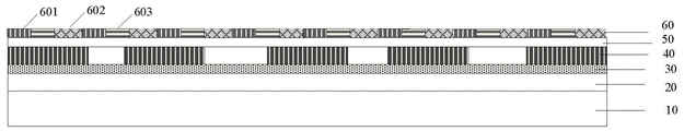
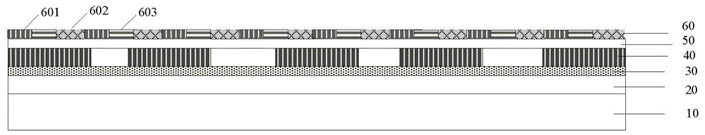
The array substrate provided by the embodiment of the invention comprises a substrate, a first electrode and a second electrode which are positioned on the substrate, a quantum rod orientation layer and a quantum rod layer positioned on the quantum rod orientation layer. Fig. 1 schematically illustrates a partial cross-sectional view of an array substrate according to an embodiment of the present disclosure. As shown in fig. 1, the array substrate includes a substrate 10, a first electrode 20 and a second electrode 40 on the substrate 10, the first electrode 20 and the second electrode 40 being configured to generate an electric field parallel to an upper surface of the substrate 10 facing the first electrode and the second electrode. The array substrate further includes a quantum rod alignment layer 50, and a quantum rod layer 60 on the quantum rod alignment layer 50, the quantum rod layer 60 having a plurality of quantum rods configured to deflect in response to an electric field generated by the first and second electrodes. By using the quantum rod layer in the array substrate shown in fig. 1 and the electrode for controlling the deflection of the quantum rod in the quantum rod layer, the liquid crystal display product to which the array substrate of the embodiment of the disclosure is applied can realize switching between a narrow viewing angle and a normal viewing angle.
The principle that the array substrate provided by the above embodiments of the present invention can provide a narrow viewing angle effect for a liquid crystal display device is specifically described below. The inventors of the present application have realized that quantum rods have the following properties: the quantum rod can emit linearly polarized light with the vibration direction parallel to the long axis and perpendicular to the short axis in response to receiving external light, namely, the linearly polarized light can be generated by the quantum rod, and the vibration direction of the linearly polarized light is parallel to the long axis direction of the quantum rod. Therefore, the quantum rod layer in the array substrate can receive external light (e.g., backlight) to generate linearly polarized light, and the array substrate provided by the embodiment of the invention does not need to include a polarizer. The quantum rod alignment layer in the array substrate is used to determine the initial orientation or azimuth of each quantum rod in the quantum rod layer, which is similar to an alignment film for liquid crystal molecules in a liquid crystal display device, and may also be referred to herein as a quantum rod alignment layer. It can be understood that the orientation of the quantum rods in the quantum rod layer is influenced by the electric field generated by the first electrode 20 and the second electrode 40, that is, when the first electrode 20 and the second electrode 40 receive a suitable voltage to generate a corresponding electric field, the quantum rods in the quantum rod layer 60 are deflected relative to their initial state due to the electric field. As described above, the quantum rod layer in the array substrate may generate linearly polarized light by receiving the backlight, and the vibration direction of the linearly polarized light is parallel to the long axis direction of the quantum rod, so that the quantum rod layer may replace the polarizer included in the conventional array substrate, and the polarization state of the linearly polarized light generated by the quantum rod layer may be controlled by the electric field generated by the first electrode and the second electrode. That is, the combination of the quantum rod layer, the first electrode and the second electrode in the array substrate proposed by the embodiments of the present disclosure can be regarded as a polarizer whose light transmission axis can be adjusted to some extent, which provides a possibility for a liquid crystal display device to which the array substrate is applied to switch between operation modes having different viewing angle ranges.
As can be understood by those skilled in the art, the array substrate and the color filter substrate of the conventional liquid crystal display device respectively include a polarizer, that is, an upper polarizer in the color filter substrate and a lower polarizer in the array substrate, and a light transmission axis of the upper polarizer and a light transmission axis of the lower polarizer are perpendicular to each other, so as to implement a normal display function. With the array substrate provided by the embodiment of the present disclosure, by controlling the electric field between the first electrode and the second electrode, the orientation of the quantum rod in the quantum rod layer can be controlled or adjusted, so that the vibration direction of the polarized light emitted from the quantum rod layer can be controlled. Therefore, for the liquid crystal display device applying the array substrate provided by the embodiment of the disclosure, the polarization state of the linearly polarized light emitted by the quantum rod layer can be the same as the linearly polarized light generated by the lower polarizer in the conventional array substrate, for example, the first electrode and the second electrode do not receive a voltage and do not generate an electric field, and at this time, the liquid crystal display device is in a normal display state, so as to provide a normal range of viewing angle for a user. On the other hand, by means of the first electrode and the second electrode, an electric field for deflecting the quantum rod in the quantum rod layer may be generated, for example, by applying a voltage to the first electrode and the second electrode to deflect the quantum rod, and the polarization state of the polarized light emitted from the quantum rod will be different from the polarization state when the liquid crystal display device normally displays, so that the vibration direction of the polarized light emitted from the quantum rod layer is not perpendicular to the light transmission axis of the upper polarizer, thereby affecting the range of the viewing angle of the liquid crystal display device. For example, when the liquid crystal display device is in a fully off state or a dark state displaying a minimum brightness value, a part of light is emitted from the upper polarizer of the liquid crystal display device, and a viewer at a side of the liquid crystal display device perceives a strong visual brightness, which reduces the contrast of the perceived image, thereby affecting the viewing effect thereof. When the liquid crystal display device displays a normal picture, for a darker display area in the picture, a viewer beside the liquid crystal display device can perceive stronger brightness, and the contrast of the picture perceived by the viewer beside the liquid crystal display device is also greatly reduced, so that the viewer is difficult to see the displayed content clearly, and the peep-proof function is realized. As for the privacy effect achieved by the liquid crystal display device, an exemplary explanation will be given below by way of a specific experiment.
Layer 60 in fig. 1 represents a quantum rod layer, and quantum rod layer 60 includes a plurality of quantum rods, which may be formed on quantum rod alignment layer 50 by inkjet printing or spin coating. These quantum rods may be orderly arranged and positioned by means of the quantum rod alignment layer 60. In some embodiments, the quantum rod layer comprises the same number of red quantum rods 601, green quantum rods 602, and blue quantum rods 603, which are alternately arranged in the same layer, in a ratio of 1: 1: 1 can be mixed to produce white light, as shown in fig. 1. The red, green and blue quantum rods mentioned herein refer to quantum rods that emit red, green and blue light, respectively, upon receiving external light. Materials from which quantum rods are fabricated include, but are not limited to, cadmium selenide (CdSe), cadmium sulfide (CdS), cadmium telluride (CdTe), zinc oxide (ZnO), zinc selenide (ZnSe), zinc sulfide (ZnS), zinc telluride (ZnTe), mercury selenide (HgSe), mercury telluride (HgTe), and the like. In the manufacture of the quantum rod, the quantum rod capable of emitting light of different colors can be obtained by considering different factors such as the size and material of the quantum rod.
In the example of fig. 1, the first electrode 20 and the second electrode 40 are arranged on the substrate 10 along a vertical direction perpendicular to the upper surface of the substrate 10, the first electrode 20 and the second electrode 40 are separated by the insulating layer 30, and the second electrode 40 includes a plurality of electrode bars spaced apart from each other, which may also be separated by an insulating material. Accordingly, when a voltage is applied to the first and second electrodes 20 and 40, the electric field generated by the first and second electrodes includes an electric field component parallel to the upper surface of the substrate 10, and the quantum rods in the quantum rod layer 60 may be deflected by the electric field.
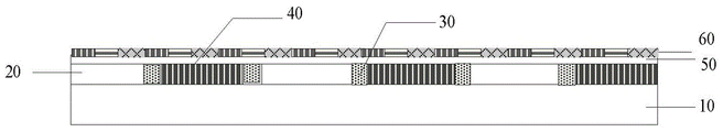
It can be appreciated that the arrangement of the first and second electrodes is not limited to the example of fig. 1 in order to deflect the quantum rods in the quantum rod layer. In fig. 1, the second electrode 40 is patterned, i.e. comprises a plurality of electrode stripes spaced apart from each other, but in further embodiments the first electrode 20 may be patterned while the second electrode 40 is one continuous whole, in which case the quantum rod alignment layer 50 and the quantum rod layer 60 may be arranged below the first electrode. Alternatively, in other embodiments, both the first and second electrodes may be patterned. For another example, in yet another embodiment of the present disclosure, the first electrode and the second electrode may be substantially in the same layer. As shown in fig. 2, each of the first and second electrodes 20 and 40 includes a plurality of electrode bars spaced apart from each other, the electrode bars in the first electrode and the electrode bars in the second electrode are alternately arranged with each other on the substrate 10 along an upper surface of the substrate 10 facing the first and second electrodes 20 and 40, and adjacent electrode bars are isolated from each other by an insulating material 30. Thus, when a voltage is applied to the first electrode and the second electrode, an electric field for deflecting the quantum rod can be generated between the adjacent electrode bars. In the example of fig. 1 and 2, the quantum rod alignment layer and the quantum rods are located above the first electrode and the second electrode. Alternatively, the quantum rod alignment layer and the quantum rod layer may also be located below the first electrode and the second electrode. Therefore, in order to realize that the quantum rod in the quantum rod layer can deflect in response to the electric field between the first electrode and the second electrode, the specific structures of the first electrode and the second electrode and the position relationship between the electrodes and the quantum rod layer can have a plurality of different design schemes, and any obvious modification or variation based on the embodiments described in the disclosure is within the protection scope of the present application. The material forming the first and second electrodes may include various transparent conductive materials, including but not limited to Indium Tin Oxide (ITO).
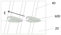
The quantum rod alignment layer 50 may determine an initial state of the quantum rods in the quantum rod layer 60, and when a voltage is applied to the first and second electrodes, an electric field generated by the first and second electrodes may deflect the quantum rods in the nano-scale. Fig. 3 schematically shows that the quantum rod 600 is deflected by the electric field E generated by the first electrode 20 and the second electrode 40. When the array substrate is applied to a liquid crystal display device, a control mechanism for controlling a voltage between the first electrode and the second electrode may be provided. For example, the presence or absence of a voltage between the first and second electrodes may be controlled by a switch, and a voltage regulator with an adjustable output voltage may be provided to provide a variable magnitude voltage to the first and second electrodes. That is, whether a voltage is present between the first electrode and the second electrode and the magnitude of the voltage can be controlled or adjusted, and accordingly, the strength of the electric field between the first electrode and the second electrode can be adjusted, and thus, whether and to what extent the quantum rods in the quantum rod layer are deflected with respect to their initial state can be controlled. Therefore, the display device applying the array substrate can be controlled to be in a normal display state with a normal viewing angle and also can be controlled to be switched to a peep-proof state with a narrow viewing angle.
The example of fig. 1 or 2 only shows a partial cross-sectional view of the array substrate according to the embodiment of the present disclosure, and the array substrate may further include any other necessary elements in order to implement a display function depending on the type of the liquid crystal display device. In some embodiments, one of the first and second electrodes is a common electrode electrically connected to a reference potential, and the array substrate further comprises a patterned pixel electrode over the quantum rod layer. Fig. 4 schematically shows such an array substrate, and in fig. 4, the first electrode 20 may be a common electrode receiving a reference potential, and the patterned pixel electrode 70 is disposed above the quantum rod layer 60. When a display device using the array substrate operates, the pixel electrode and the common electrode may generate another electric field for deflecting liquid crystal molecules above the array substrate, i.e., the display device actually constitutes an ADS mode display device. It can be understood that the electric field for deflecting the quantum rods in the quantum rod layer and the other electric field for deflecting the liquid crystal molecules are independent of each other. In the example of fig. 4, the pixel electrode 70 and the second electrode 40 actually share one common electrode 20, and in other embodiments, another common electrode may be provided that exclusively cooperates with the pixel electrode 70 to generate an electric field for deflecting liquid crystal molecules. Furthermore, it can be appreciated that any suitable intermediate layer may be present between the quantum rod layer 60 and the pixel electrode 70 to provide a protective effect to the quantum rod layer.
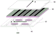
Another embodiment of the present disclosure provides a liquid crystal display panel, which includes the array substrate and the color filter substrate according to any of the embodiments. The principle that the array substrate described herein can provide a privacy function to the liquid crystal display device can be more clearly understood through the following detailed description of the embodiments of the liquid crystal display panel. Fig. 5 schematically shows a partial structure view of a liquid crystal display panel provided according to an embodiment of the present disclosure, and in fig. 5, the substrate 10 in the array substrate, the second electrode 40 including a plurality of electrode stripes separated from each other, the color film layer 80 in the color film substrate, and the polarizer 90 are schematically shown. Also shown in fig. 5 are the direction P in which the light transmission axis of the polarizer 90 is located and the initial direction a of the long axis direction of the quantum rods in the quantum rod layer. In this embodiment, the quantum rod alignment layer in the array substrate is configured such that the initial alignment a of the long axis direction of the quantum rods in the quantum rod layer is perpendicular to the light transmission axis P of the polarizer 90. Therefore, the vibration direction of the linearly polarized light emitted from the quantum rod layer is perpendicular to the light transmission axis of the polarizer on the color film substrate, so as to implement a normal display function, or in this embodiment, the quantum rod layer implements a function of a lower polarizer generally included in a conventional liquid crystal display panel. Also, in this example, the angle θ between the extending direction of the electrode stripes in the first electrode or the second electrode and the initial direction a of the long axis direction of the quantum rods in the quantum rod layer is deviated by 90 degrees. In this way, the quantum rod can be more easily deflected when being subjected to the electric field generated by the first electrode and the second electrode, so that the orientation of the long axis direction of the quantum rod in the quantum rod layer is not perpendicular to the light transmission axis P of the polarizer 90, thereby realizing the peep-proof effect. .
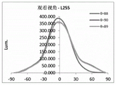
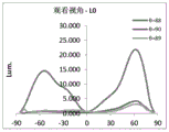
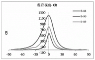
As described above, the privacy effect can be achieved by setting the vibration direction of the polarized light emitted from the quantum rod layer to be non-perpendicular to the light transmission axis of the polarizer on the color film substrate of the liquid crystal display device. The inventor of the present application performed a simulation experiment on this, and applied a voltage to the first electrode and the second electrode to deflect the quantum rod in the quantum rod layer, so that an included angle between the long axis direction of the quantum rod and the light transmission axis of the polarizer deviates by 90 degrees. The inventors of the present application have simulated different cases when the included angles between the long axis direction of the quantum rod and the light transmission axis of the polarizer were 88 degrees, 89 degrees, and 90 degrees, respectively. Fig. 6 shows a relationship between a viewing angle and a visual brightness at a maximum brightness value of a liquid crystal display device to which the array substrate of the embodiment of the present disclosure is applied, and fig. 7 shows a relationship between a viewing angle and a visual brightness at a minimum brightness value of a liquid crystal display device to which the array substrate of the embodiment of the present disclosure is applied. As can be seen from fig. 6, when the liquid crystal display device is controlled to be at the highest display luminance, a normal user who can normally look at the screen of the liquid crystal display device can perceive a higher visual luminance. When the included angle between the long axis direction of the quantum rod and the light transmission axis of the polarizer is reduced to 88 degrees, the visual brightness perceived by a viewer at the side is reduced. As shown in fig. 7, the liquid crystal display device is controlled to have the lowest display brightness, and when the angle between the long axis direction of the quantum rod and the light transmission axis of the polarizer is 90 degrees or 89 degrees, the visual brightness perceived by a normal user looking at the screen of the liquid crystal display device and a viewer beside the screen is low. However, when the angle between the long axis of the quantum rod and the light transmission axis of the polarizer is 88 degrees, the viewer at the side can perceive a significant visual brightness. Further, fig. 8 shows the relationship between the contrast and the viewing angle for different cases in which the long axis direction of the quantum rod and the light transmission axis of the polarizer are at angles of 88 degrees, 89 degrees and 90 degrees, respectively. In fig. 6 to 8, 0 in the abscissa corresponds to the middle position of the center of the screen of the front-view-able liquid crystal display panel where the user is located, and other numerical values on the abscissa indicate the distance to the middle position. As can be seen from fig. 8, when the angle between the long axis direction of the quantum rod and the light transmission axis of the polarizer gradually decreases from 90 degrees, the contrast of the image perceived by the side viewer far from the middle position sharply decreases, so that the side viewer cannot clearly see the displayed content, thereby achieving the peep-proof effect. However, in the simulation example of fig. 8, as the angle between the long axis direction of the quantum rod and the light transmission axis of the polarizer gradually deviates from 90 degrees, the contrast perceived by a user at an intermediate position also decreases, and the angle between the long axis direction of the quantum rod and the light transmission axis of the polarizer is not preferably excessively shifted by 90 degrees so as not to affect the viewing effect of a normal user of the display device.
The angle between the long axis direction of the quantum rod and the light transmission axis of the polarizer can be realized by adjusting the intensity of the electric field between the first electrode and the second electrode, and the intensity of the electric field between the first electrode and the second electrode is related to the magnitude of the voltage supplied to the first electrode and the second electrode. In addition, under the condition that no voltage is applied to the first electrode and the second electrode, the quantum rod in the quantum rod layer can not be deflected, the vibration direction of linear polarized light emitted from the quantum rod layer is vertical to the light transmission axis of the polaroid, and the liquid crystal display device has a normal viewing angle. That is, the peep prevention function of the liquid crystal display device is not turned on at this time, which is applicable to a case where there is no need to worry about that the displayed content is known to others, for example, viewing behavior in a private space, or a case where it is desired that the displayed content is seen by more people. Therefore, according to one embodiment of the present disclosure, a liquid crystal display panel includes a controller configured to control whether to apply a voltage to a first electrode and a second electrode. For example, the controller may include a switching element that controls whether the first and second electrodes are connected to a circuit for supplying a voltage, thereby conveniently turning on or off a peep prevention function of the liquid crystal display device. The controller can be arranged at any suitable position of the liquid crystal display panel, for example, as an accessory component of the array substrate or the color film substrate, and also as a separate component independent of the array substrate and the color film substrate in the liquid crystal display device.
Further, in further embodiments, the controller may include a voltage regulator configured to provide a regulated voltage to the first and second electrodes, the first and second electrodes generating the electric field in response to receiving the regulated voltage such that an angle between an orientation of a long axis direction of the quantum rods in the sub-rod layer and a light transmission axis of the polarizer is greater than 85 degrees and less than 90 degrees. Therefore, the influence on the normal watching effect of the user of the display device can be reduced on the premise of the peep-proof effect. That is, in this embodiment, fine adjustment of the peep prevention effect can be achieved by adjusting the magnitude of the voltage supplied to the first electrode and the second electrode by the controller, whereby dynamic adjustment of the viewable viewing angle range of the liquid crystal display device can also be achieved, achieving viewing angles of different ranges. In practice, a switch or a button for operating the controller may be provided on an outer surface or a display screen of the liquid crystal display device, facilitating a user's flexible control over whether to activate the anti-peeping function of the liquid crystal display device and over the viewable viewing angle range of the liquid crystal display device.
Fig. 9 schematically illustrates a partial structural view of an array substrate in a liquid crystal display panel according to another embodiment of the present disclosure. Unlike the previous embodiments, in this embodiment, the quantum rod layer includes a first sub-quantum rod layer and a second sub-quantum rod layer above the first sub-quantum rod layer. The first sub-quantum rod layer comprises a first quantum rod, the second sub-quantum rod layer comprises a second quantum rod and a third quantum rod, and the first quantum rod, the second quantum rod and the third quantum rod are selected from a red quantum rod, a blue quantum rod and a green quantum rod and are different from each other. As shown in fig. 9, the quantum rods in the first sub-quantum rod layer are all composed of red quantum rods 601, and the second sub-quantum rod layer is disposed on another quantum rod alignment layer 50a, which includes green quantum rods 602 and blue quantum rods 603, so that the first sub-quantum rod layer can emit linearly polarized light of a single color (e.g., red light), and the second sub-quantum rod layer absorbs the linearly polarized light of the single color to emit linearly polarized light of a corresponding color. Alternatively, the first sub-quantum rod layer is composed entirely of blue quantum rods, and the second sub-quantum rod layer includes red quantum rods and green quantum rods, so that the second sub-quantum rod layer can absorb linearly polarized blue light to emit linearly polarized red light and green light. Therefore, the first sub-quantum rod layer actually has the function of filtering partial wavelength light to obtain single wavelength light, so that the wavelength of the light emitted by each pixel of the display panel is more concentrated in a certain wavelength range, and the color gamut of the display picture of the display panel is favorably improved.
Further, as shown in fig. 9, the second sub-quantum rod layer includes a plurality of quantum rod groups, each quantum rod group includes one second quantum rod 602 and one third quantum rod 603, and a light-transmitting layer 604 is provided between each adjacent two quantum rod groups. That is, in the embodiment of fig. 9, the second quantum rod 602, the third quantum rod 603, and the light transmissive layer 604 constitute a repeating unit of the second sub-quantum rod layer. The second quantum rod 602 and the third quantum rod 603 may absorb the light of a single color emitted from the first sub-quantum rod layer to emit light of different colors, and the light-transmitting layer 604 in the second sub-quantum rod layer may allow the light of a single color emitted from the first sub-quantum rod layer to pass through. In addition, in this case, the numbers of the second quantum rods, the third quantum rods and the light-transmitting layer in the second sub-quantum rod layer are equal, which is advantageous for achieving uniformity of light of different colors emitted from the second sub-quantum rod layer. In fig. 9, the second quantum rod, the third quantum rod, and the light-transmitting layer are spaced apart from each other by light-blocking materials, which form a black matrix. Therefore, in this case, sub-pixel regions displaying different colors are actually formed, and the color filter substrate may not have a color filter layer. For the example of the array substrate shown in fig. 9, the liquid crystal display panel can also be made to perform normal display and anti-peep functions, and the principle is similar to that of the foregoing embodiment. It can be understood that, for the first sub-quantum rod layer and the second sub-quantum rod layer, the orientation of the quantum rod in only one of the layers may be controlled, while the orientation of the quantum rod in the other sub-quantum rod layer is fixed, or the orientations of the quantum rods in both the first sub-quantum rod layer and the second sub-quantum rod layer may be controlled at the same time, so as to achieve the technical effect of peep prevention. For example, in the case where the orientations of the quantum rods 602 and 603 in the second sub-quantum rod layer are fixed, the orientation of the first sub-quantum rod 601 in the first sub-quantum rod layer may be controlled in a similar manner as for the quantum rod layer 60 in fig. 1, 2, or 5 to achieve normal display and privacy display, because a part of the light emitted from the first sub-quantum rod layer may be transmitted through the light transmitting layer 604 in the second sub-quantum rod layer.
In the example of fig. 9, the second sub-quantum rod layer is remote from the first and second electrodes, the first and second electrodes 20 and 40 may change the orientation of the first quantum rod in the first sub-quantum rod layer, and the second and third quantum rods in the second sub-quantum rod layer have fixed orientations. That is, the long axis directions of the second and third quantum rods are fixed to be perpendicular to the light transmission axis of the polarizer on the color film substrate of the display panel, and the orientation of the first quantum rod in the first sub-quantum rod layer may be controlled, but the initial orientation thereof is perpendicular to the light transmission axis of the polarizer. Alternatively, the positions of the first and second electrodes may be modified such that the orientation of the quantum rods in the second sub-quantum rod layer is controlled by the electric field generated by the first and second electrodes, and the orientation of the first quantum rods in the first sub-quantum rod layer is fixed (not affected by the electric field), i.e., the long axis direction of the first quantum rods is perpendicular to the light transmission axis of the polarizer on the color filter substrate of the display panel. Alternatively, additional electrodes may be disposed in the array substrate to achieve separate control of the first and second sub-quantum rod layers. Also, in addition to the quantum rod alignment layer 50a, any other necessary layer structure may exist between the first sub-quantum layer and the second sub-quantum rod layer. These are all obvious variations to the embodiment shown in fig. 9 and fall within the scope of protection of the present application.
Yet another embodiment of the present disclosure provides a liquid crystal display device including the liquid crystal display panel according to the foregoing embodiments. It can be understood that the liquid crystal display device has the same technical effects as the liquid crystal display panel, and the details are not repeated herein.
While certain exemplary embodiments of the invention have been described in detail above, other variations to the disclosed embodiments can be understood and effected by those skilled in the art in practicing the claimed invention, from a study of the drawings, the disclosure, and the appended claims. In the claims, the word "comprising" does not exclude the presence of other elements. Although some features are recited in different dependent claims, the invention is also intended to cover embodiments in which these features are combined together.