CN109891651B - Power storage device and method for manufacturing power storage device - Google Patents
Power storage device and method for manufacturing power storage device Download PDFInfo
- Publication number
- CN109891651B CN109891651B CN201780062803.1A CN201780062803A CN109891651B CN 109891651 B CN109891651 B CN 109891651B CN 201780062803 A CN201780062803 A CN 201780062803A CN 109891651 B CN109891651 B CN 109891651B
- Authority
- CN
- China
- Prior art keywords
- resin member
- bipolar electrodes
- current collector
- bipolar
- electrode layer
- Prior art date
- Legal status (The legal status is an assumption and is not a legal conclusion. Google has not performed a legal analysis and makes no representation as to the accuracy of the status listed.)
- Active
Links
- 238000003860 storage Methods 0.000 title claims abstract description 49
- 238000000034 method Methods 0.000 title claims description 16
- 238000004519 manufacturing process Methods 0.000 title claims description 15
- 239000011347 resin Substances 0.000 claims abstract description 159
- 229920005989 resin Polymers 0.000 claims abstract description 159
- 230000002093 peripheral effect Effects 0.000 claims abstract description 25
- 239000000463 material Substances 0.000 claims description 14
- 238000003466 welding Methods 0.000 claims description 13
- 238000001746 injection moulding Methods 0.000 claims description 9
- 230000005611 electricity Effects 0.000 claims description 7
- 238000010030 laminating Methods 0.000 claims description 7
- 239000012530 fluid Substances 0.000 claims description 4
- 239000007773 negative electrode material Substances 0.000 claims description 4
- 239000007774 positive electrode material Substances 0.000 claims description 4
- 238000010438 heat treatment Methods 0.000 claims description 3
- -1 polypropylene Polymers 0.000 description 11
- 239000004743 Polypropylene Substances 0.000 description 8
- 229920001155 polypropylene Polymers 0.000 description 8
- 238000006073 displacement reaction Methods 0.000 description 7
- OKTJSMMVPCPJKN-UHFFFAOYSA-N Carbon Chemical compound [C] OKTJSMMVPCPJKN-UHFFFAOYSA-N 0.000 description 4
- 239000003792 electrolyte Substances 0.000 description 4
- 125000006850 spacer group Chemical group 0.000 description 4
- HBBGRARXTFLTSG-UHFFFAOYSA-N Lithium ion Chemical compound [Li+] HBBGRARXTFLTSG-UHFFFAOYSA-N 0.000 description 3
- PXHVJJICTQNCMI-UHFFFAOYSA-N Nickel Chemical compound [Ni] PXHVJJICTQNCMI-UHFFFAOYSA-N 0.000 description 3
- KWYUFKZDYYNOTN-UHFFFAOYSA-M Potassium hydroxide Chemical compound [OH-].[K+] KWYUFKZDYYNOTN-UHFFFAOYSA-M 0.000 description 3
- 230000000694 effects Effects 0.000 description 3
- 229910001416 lithium ion Inorganic materials 0.000 description 3
- 230000004048 modification Effects 0.000 description 3
- 238000012986 modification Methods 0.000 description 3
- 238000000465 moulding Methods 0.000 description 3
- 229920002647 polyamide Polymers 0.000 description 3
- WHXSMMKQMYFTQS-UHFFFAOYSA-N Lithium Chemical compound [Li] WHXSMMKQMYFTQS-UHFFFAOYSA-N 0.000 description 2
- 239000004952 Polyamide Substances 0.000 description 2
- 239000004734 Polyphenylene sulfide Substances 0.000 description 2
- 229910052799 carbon Inorganic materials 0.000 description 2
- 230000004927 fusion Effects 0.000 description 2
- 229910002804 graphite Inorganic materials 0.000 description 2
- 239000010439 graphite Substances 0.000 description 2
- 229910052739 hydrogen Inorganic materials 0.000 description 2
- 239000001257 hydrogen Substances 0.000 description 2
- 230000001678 irradiating effect Effects 0.000 description 2
- 238000003475 lamination Methods 0.000 description 2
- 229910052744 lithium Inorganic materials 0.000 description 2
- 229910052751 metal Inorganic materials 0.000 description 2
- 239000002184 metal Substances 0.000 description 2
- 229910052987 metal hydride Inorganic materials 0.000 description 2
- 239000002245 particle Substances 0.000 description 2
- 229920001707 polybutylene terephthalate Polymers 0.000 description 2
- 229920000069 polyphenylene sulfide Polymers 0.000 description 2
- BQCIDUSAKPWEOX-UHFFFAOYSA-N 1,1-Difluoroethene Chemical compound FC(F)=C BQCIDUSAKPWEOX-UHFFFAOYSA-N 0.000 description 1
- ZOXJGFHDIHLPTG-UHFFFAOYSA-N Boron Chemical compound [B] ZOXJGFHDIHLPTG-UHFFFAOYSA-N 0.000 description 1
- UFHFLCQGNIYNRP-UHFFFAOYSA-N Hydrogen Chemical compound [H][H] UFHFLCQGNIYNRP-UHFFFAOYSA-N 0.000 description 1
- DGAQECJNVWCQMB-PUAWFVPOSA-M Ilexoside XXIX Chemical compound C[C@@H]1CC[C@@]2(CC[C@@]3(C(=CC[C@H]4[C@]3(CC[C@@H]5[C@@]4(CC[C@@H](C5(C)C)OS(=O)(=O)[O-])C)C)[C@@H]2[C@]1(C)O)C)C(=O)O[C@H]6[C@@H]([C@H]([C@@H]([C@H](O6)CO)O)O)O.[Na+] DGAQECJNVWCQMB-PUAWFVPOSA-M 0.000 description 1
- 239000004698 Polyethylene Substances 0.000 description 1
- 239000004642 Polyimide Substances 0.000 description 1
- 239000004793 Polystyrene Substances 0.000 description 1
- NINIDFKCEFEMDL-UHFFFAOYSA-N Sulfur Chemical compound [S] NINIDFKCEFEMDL-UHFFFAOYSA-N 0.000 description 1
- 239000003513 alkali Substances 0.000 description 1
- 229910052783 alkali metal Inorganic materials 0.000 description 1
- 150000001340 alkali metals Chemical class 0.000 description 1
- 239000000956 alloy Substances 0.000 description 1
- 229910045601 alloy Inorganic materials 0.000 description 1
- 239000007864 aqueous solution Substances 0.000 description 1
- 239000004760 aramid Substances 0.000 description 1
- 229920006231 aramid fiber Polymers 0.000 description 1
- 229910052796 boron Inorganic materials 0.000 description 1
- 239000003990 capacitor Substances 0.000 description 1
- 239000002131 composite material Substances 0.000 description 1
- 150000001875 compounds Chemical class 0.000 description 1
- 239000011888 foil Substances 0.000 description 1
- 229910021385 hard carbon Inorganic materials 0.000 description 1
- 238000009413 insulation Methods 0.000 description 1
- 239000002931 mesocarbon microbead Substances 0.000 description 1
- 150000002736 metal compounds Chemical class 0.000 description 1
- 229910052759 nickel Inorganic materials 0.000 description 1
- AIBQNUOBCRIENU-UHFFFAOYSA-N nickel;dihydrate Chemical compound O.O.[Ni] AIBQNUOBCRIENU-UHFFFAOYSA-N 0.000 description 1
- 239000004745 nonwoven fabric Substances 0.000 description 1
- 229920000927 poly(p-phenylene benzobisoxazole) Polymers 0.000 description 1
- 229920002577 polybenzoxazole Polymers 0.000 description 1
- 239000004417 polycarbonate Substances 0.000 description 1
- 229920000515 polycarbonate Polymers 0.000 description 1
- 229920000573 polyethylene Polymers 0.000 description 1
- 229920001721 polyimide Polymers 0.000 description 1
- 229920000098 polyolefin Polymers 0.000 description 1
- 238000002360 preparation method Methods 0.000 description 1
- 230000000452 restraining effect Effects 0.000 description 1
- 229910052708 sodium Inorganic materials 0.000 description 1
- 239000011734 sodium Substances 0.000 description 1
- 229910021384 soft carbon Inorganic materials 0.000 description 1
- 239000000243 solution Substances 0.000 description 1
- 229910052717 sulfur Inorganic materials 0.000 description 1
- 239000011593 sulfur Substances 0.000 description 1
Images


Classifications
-
- H—ELECTRICITY
- H01—ELECTRIC ELEMENTS
- H01M—PROCESSES OR MEANS, e.g. BATTERIES, FOR THE DIRECT CONVERSION OF CHEMICAL ENERGY INTO ELECTRICAL ENERGY
- H01M4/00—Electrodes
- H01M4/02—Electrodes composed of, or comprising, active material
- H01M4/64—Carriers or collectors
- H01M4/70—Carriers or collectors characterised by shape or form
-
- H—ELECTRICITY
- H01—ELECTRIC ELEMENTS
- H01G—CAPACITORS; CAPACITORS, RECTIFIERS, DETECTORS, SWITCHING DEVICES, LIGHT-SENSITIVE OR TEMPERATURE-SENSITIVE DEVICES OF THE ELECTROLYTIC TYPE
- H01G11/00—Hybrid capacitors, i.e. capacitors having different positive and negative electrodes; Electric double-layer [EDL] capacitors; Processes for the manufacture thereof or of parts thereof
- H01G11/10—Multiple hybrid or EDL capacitors, e.g. arrays or modules
- H01G11/12—Stacked hybrid or EDL capacitors
-
- H—ELECTRICITY
- H01—ELECTRIC ELEMENTS
- H01G—CAPACITORS; CAPACITORS, RECTIFIERS, DETECTORS, SWITCHING DEVICES, LIGHT-SENSITIVE OR TEMPERATURE-SENSITIVE DEVICES OF THE ELECTROLYTIC TYPE
- H01G11/00—Hybrid capacitors, i.e. capacitors having different positive and negative electrodes; Electric double-layer [EDL] capacitors; Processes for the manufacture thereof or of parts thereof
- H01G11/74—Terminals, e.g. extensions of current collectors
- H01G11/76—Terminals, e.g. extensions of current collectors specially adapted for integration in multiple or stacked hybrid or EDL capacitors
-
- H—ELECTRICITY
- H01—ELECTRIC ELEMENTS
- H01G—CAPACITORS; CAPACITORS, RECTIFIERS, DETECTORS, SWITCHING DEVICES, LIGHT-SENSITIVE OR TEMPERATURE-SENSITIVE DEVICES OF THE ELECTROLYTIC TYPE
- H01G11/00—Hybrid capacitors, i.e. capacitors having different positive and negative electrodes; Electric double-layer [EDL] capacitors; Processes for the manufacture thereof or of parts thereof
- H01G11/78—Cases; Housings; Encapsulations; Mountings
- H01G11/80—Gaskets; Sealings
-
- H—ELECTRICITY
- H01—ELECTRIC ELEMENTS
- H01G—CAPACITORS; CAPACITORS, RECTIFIERS, DETECTORS, SWITCHING DEVICES, LIGHT-SENSITIVE OR TEMPERATURE-SENSITIVE DEVICES OF THE ELECTROLYTIC TYPE
- H01G11/00—Hybrid capacitors, i.e. capacitors having different positive and negative electrodes; Electric double-layer [EDL] capacitors; Processes for the manufacture thereof or of parts thereof
- H01G11/78—Cases; Housings; Encapsulations; Mountings
- H01G11/82—Fixing or assembling a capacitive element in a housing, e.g. mounting electrodes, current collectors or terminals in containers or encapsulations
-
- H—ELECTRICITY
- H01—ELECTRIC ELEMENTS
- H01G—CAPACITORS; CAPACITORS, RECTIFIERS, DETECTORS, SWITCHING DEVICES, LIGHT-SENSITIVE OR TEMPERATURE-SENSITIVE DEVICES OF THE ELECTROLYTIC TYPE
- H01G11/00—Hybrid capacitors, i.e. capacitors having different positive and negative electrodes; Electric double-layer [EDL] capacitors; Processes for the manufacture thereof or of parts thereof
- H01G11/84—Processes for the manufacture of hybrid or EDL capacitors, or components thereof
- H01G11/86—Processes for the manufacture of hybrid or EDL capacitors, or components thereof specially adapted for electrodes
-
- H—ELECTRICITY
- H01—ELECTRIC ELEMENTS
- H01M—PROCESSES OR MEANS, e.g. BATTERIES, FOR THE DIRECT CONVERSION OF CHEMICAL ENERGY INTO ELECTRICAL ENERGY
- H01M10/00—Secondary cells; Manufacture thereof
- H01M10/04—Construction or manufacture in general
-
- H—ELECTRICITY
- H01—ELECTRIC ELEMENTS
- H01M—PROCESSES OR MEANS, e.g. BATTERIES, FOR THE DIRECT CONVERSION OF CHEMICAL ENERGY INTO ELECTRICAL ENERGY
- H01M10/00—Secondary cells; Manufacture thereof
- H01M10/04—Construction or manufacture in general
- H01M10/0413—Large-sized flat cells or batteries for motive or stationary systems with plate-like electrodes
- H01M10/0418—Large-sized flat cells or batteries for motive or stationary systems with plate-like electrodes with bipolar electrodes
-
- H—ELECTRICITY
- H01—ELECTRIC ELEMENTS
- H01M—PROCESSES OR MEANS, e.g. BATTERIES, FOR THE DIRECT CONVERSION OF CHEMICAL ENERGY INTO ELECTRICAL ENERGY
- H01M10/00—Secondary cells; Manufacture thereof
- H01M10/04—Construction or manufacture in general
- H01M10/0486—Frames for plates or membranes
-
- H—ELECTRICITY
- H01—ELECTRIC ELEMENTS
- H01M—PROCESSES OR MEANS, e.g. BATTERIES, FOR THE DIRECT CONVERSION OF CHEMICAL ENERGY INTO ELECTRICAL ENERGY
- H01M10/00—Secondary cells; Manufacture thereof
- H01M10/05—Accumulators with non-aqueous electrolyte
- H01M10/052—Li-accumulators
- H01M10/0525—Rocking-chair batteries, i.e. batteries with lithium insertion or intercalation in both electrodes; Lithium-ion batteries
-
- H—ELECTRICITY
- H01—ELECTRIC ELEMENTS
- H01M—PROCESSES OR MEANS, e.g. BATTERIES, FOR THE DIRECT CONVERSION OF CHEMICAL ENERGY INTO ELECTRICAL ENERGY
- H01M10/00—Secondary cells; Manufacture thereof
- H01M10/05—Accumulators with non-aqueous electrolyte
- H01M10/058—Construction or manufacture
- H01M10/0585—Construction or manufacture of accumulators having only flat construction elements, i.e. flat positive electrodes, flat negative electrodes and flat separators
-
- H—ELECTRICITY
- H01—ELECTRIC ELEMENTS
- H01M—PROCESSES OR MEANS, e.g. BATTERIES, FOR THE DIRECT CONVERSION OF CHEMICAL ENERGY INTO ELECTRICAL ENERGY
- H01M10/00—Secondary cells; Manufacture thereof
- H01M10/24—Alkaline accumulators
- H01M10/30—Nickel accumulators
-
- H—ELECTRICITY
- H01—ELECTRIC ELEMENTS
- H01M—PROCESSES OR MEANS, e.g. BATTERIES, FOR THE DIRECT CONVERSION OF CHEMICAL ENERGY INTO ELECTRICAL ENERGY
- H01M4/00—Electrodes
- H01M4/02—Electrodes composed of, or comprising, active material
- H01M4/64—Carriers or collectors
-
- H—ELECTRICITY
- H01—ELECTRIC ELEMENTS
- H01M—PROCESSES OR MEANS, e.g. BATTERIES, FOR THE DIRECT CONVERSION OF CHEMICAL ENERGY INTO ELECTRICAL ENERGY
- H01M50/00—Constructional details or processes of manufacture of the non-active parts of electrochemical cells other than fuel cells, e.g. hybrid cells
- H01M50/10—Primary casings; Jackets or wrappings
- H01M50/102—Primary casings; Jackets or wrappings characterised by their shape or physical structure
- H01M50/103—Primary casings; Jackets or wrappings characterised by their shape or physical structure prismatic or rectangular
-
- H—ELECTRICITY
- H01—ELECTRIC ELEMENTS
- H01M—PROCESSES OR MEANS, e.g. BATTERIES, FOR THE DIRECT CONVERSION OF CHEMICAL ENERGY INTO ELECTRICAL ENERGY
- H01M50/00—Constructional details or processes of manufacture of the non-active parts of electrochemical cells other than fuel cells, e.g. hybrid cells
- H01M50/50—Current conducting connections for cells or batteries
- H01M50/572—Means for preventing undesired use or discharge
- H01M50/584—Means for preventing undesired use or discharge for preventing incorrect connections inside or outside the batteries
- H01M50/586—Means for preventing undesired use or discharge for preventing incorrect connections inside or outside the batteries inside the batteries, e.g. incorrect connections of electrodes
-
- H—ELECTRICITY
- H01—ELECTRIC ELEMENTS
- H01M—PROCESSES OR MEANS, e.g. BATTERIES, FOR THE DIRECT CONVERSION OF CHEMICAL ENERGY INTO ELECTRICAL ENERGY
- H01M50/00—Constructional details or processes of manufacture of the non-active parts of electrochemical cells other than fuel cells, e.g. hybrid cells
- H01M50/50—Current conducting connections for cells or batteries
- H01M50/572—Means for preventing undesired use or discharge
- H01M50/584—Means for preventing undesired use or discharge for preventing incorrect connections inside or outside the batteries
- H01M50/59—Means for preventing undesired use or discharge for preventing incorrect connections inside or outside the batteries characterised by the protection means
- H01M50/593—Spacers; Insulating plates
-
- H—ELECTRICITY
- H01—ELECTRIC ELEMENTS
- H01M—PROCESSES OR MEANS, e.g. BATTERIES, FOR THE DIRECT CONVERSION OF CHEMICAL ENERGY INTO ELECTRICAL ENERGY
- H01M4/00—Electrodes
- H01M4/02—Electrodes composed of, or comprising, active material
- H01M2004/026—Electrodes composed of, or comprising, active material characterised by the polarity
- H01M2004/029—Bipolar electrodes
-
- Y—GENERAL TAGGING OF NEW TECHNOLOGICAL DEVELOPMENTS; GENERAL TAGGING OF CROSS-SECTIONAL TECHNOLOGIES SPANNING OVER SEVERAL SECTIONS OF THE IPC; TECHNICAL SUBJECTS COVERED BY FORMER USPC CROSS-REFERENCE ART COLLECTIONS [XRACs] AND DIGESTS
- Y02—TECHNOLOGIES OR APPLICATIONS FOR MITIGATION OR ADAPTATION AGAINST CLIMATE CHANGE
- Y02E—REDUCTION OF GREENHOUSE GAS [GHG] EMISSIONS, RELATED TO ENERGY GENERATION, TRANSMISSION OR DISTRIBUTION
- Y02E60/00—Enabling technologies; Technologies with a potential or indirect contribution to GHG emissions mitigation
- Y02E60/10—Energy storage using batteries
-
- Y—GENERAL TAGGING OF NEW TECHNOLOGICAL DEVELOPMENTS; GENERAL TAGGING OF CROSS-SECTIONAL TECHNOLOGIES SPANNING OVER SEVERAL SECTIONS OF THE IPC; TECHNICAL SUBJECTS COVERED BY FORMER USPC CROSS-REFERENCE ART COLLECTIONS [XRACs] AND DIGESTS
- Y02—TECHNOLOGIES OR APPLICATIONS FOR MITIGATION OR ADAPTATION AGAINST CLIMATE CHANGE
- Y02P—CLIMATE CHANGE MITIGATION TECHNOLOGIES IN THE PRODUCTION OR PROCESSING OF GOODS
- Y02P70/00—Climate change mitigation technologies in the production process for final industrial or consumer products
- Y02P70/50—Manufacturing or production processes characterised by the final manufactured product
Landscapes
- Engineering & Computer Science (AREA)
- Power Engineering (AREA)
- Chemical & Material Sciences (AREA)
- Chemical Kinetics & Catalysis (AREA)
- Electrochemistry (AREA)
- General Chemical & Material Sciences (AREA)
- Microelectronics & Electronic Packaging (AREA)
- Manufacturing & Machinery (AREA)
- Materials Engineering (AREA)
- Secondary Cells (AREA)
- Electric Double-Layer Capacitors Or The Like (AREA)
- Sealing Battery Cases Or Jackets (AREA)
- Cell Electrode Carriers And Collectors (AREA)
- Connection Of Batteries Or Terminals (AREA)
Abstract
The power storage device is provided with: a plurality of bipolar electrodes which are stacked, each of the plurality of bipolar electrodes having a current collector, a positive electrode layer, and a negative electrode layer, the current collector having a 1 st surface and a 2 nd surface opposite to the 1 st surface, the positive electrode layer being provided on the 1 st surface, the negative electrode layer being provided on the 2 nd surface; a 1 st resin member provided on at least one of a 1 st surface and a 2 nd surface in at least a part of an outer peripheral portion of the current collector; and a 2 nd resin member provided on the 1 st resin member and supporting an outer peripheral portion of the current collector via the 1 st resin member. The 1 st resin members of the bipolar electrodes adjacent to each other in the stacking direction of the plurality of bipolar electrodes are connected to each other by a welded portion.
Description
Technical Field
One aspect of the invention relates to an electricity storage device and a method of manufacturing the electricity storage device.
Background
A bipolar battery is known which includes a bipolar electrode having a positive electrode formed on one surface of a current collector and a negative electrode formed on the other surface. In a bipolar battery, a plurality of bipolar electrodes are stacked in series with an electrolyte layer interposed therebetween.
For example, in the bipolar battery disclosed in patent document 1, a polypropylene layer covers the periphery of a bipolar plate (collector) using a metal such as nickel. The polypropylene layer and the unit case made of polypropylene for supporting the plurality of current collectors are fixed by integral molding. When the polypropylene layer and the cell case are integrally molded, the bipolar plate coated with the polypropylene layer is placed in a mold, and injection molding (insert molding) is performed by flowing polypropylene into the mold.
Documents of the prior art
Patent document
Patent document 1: japanese unexamined patent publication No. 2005-135764
Disclosure of Invention
Problems to be solved by the invention
When a plurality of bipolar plates are stacked and arranged in a mold for injection molding, the position of the adjacent bipolar plates may be displaced by the pressure of polypropylene flowing into the mold.
An object of one aspect of the present invention is to provide an electric storage device in which positional displacement between adjacent bipolar electrodes is suppressed, and a method for manufacturing the electric storage device.
Means for solving the problems
An electric storage device according to an aspect of the present invention includes: a plurality of bipolar electrodes which are stacked, each of the plurality of bipolar electrodes having a current collector, a positive electrode layer, and a negative electrode layer, the current collector having a 1 st surface and a 2 nd surface opposite to the 1 st surface, the positive electrode layer being provided on the 1 st surface, and the negative electrode layer being provided on the 2 nd surface; a 1 st resin member provided on at least one of the 1 st surface and the 2 nd surface in at least a part of an outer peripheral portion of the current collector; and a 2 nd resin member that is provided on the 1 st resin member, supports the outer peripheral portion of the collector via the 1 st resin member, and connects the 1 st resin members of the bipolar electrodes adjacent to each other in the stacking direction of the plurality of bipolar electrodes to each other by a welded portion.
In the above-described power storage device, the 1 st resin members of the bipolar electrodes adjacent in the stacking direction of the plurality of bipolar electrodes are connected to each other by the welded portion. Therefore, even if pressure is applied to the bipolar electrodes when the 2 nd resin member is formed, positional displacement between the adjacent bipolar electrodes can be suppressed.
The 2 nd resin member may cover an outer side of the 1 st resin member.
The welded portion may be provided on an outer end surface of the 1 st resin member, and may extend from one bipolar electrode to the other bipolar electrode in the stacking direction of the plurality of bipolar electrodes.
The welded portion may be cylindrical and arranged to surround the entire periphery of the outer peripheral portion of the current collector.
The welded portion may be disposed on each side of the current collector having a rectangular shape when viewed from a stacking direction of the plurality of bipolar electrodes.
In this case, the effect of suppressing the positional shift between the adjacent bipolar electrodes is greater than in the case where the welded portions are disposed at the respective apexes of the current collector.
In a method for manufacturing an electricity storage device according to an aspect of the present invention, the electricity storage device includes a plurality of stacked bipolar electrodes, each of the plurality of bipolar electrodes includes a current collector, a positive electrode layer, and a negative electrode layer, the current collector includes a 1 st surface and a 2 nd surface opposite to the 1 st surface, the positive electrode layer is provided on the 1 st surface, and the negative electrode layer is provided on the 2 nd surface, and the method includes: a step of providing a 1 st resin member on at least one of the 1 st surface and the 2 nd surface in at least a part of an outer peripheral portion of the current collector of each of the plurality of bipolar electrodes; a step of laminating the plurality of bipolar electrodes; welding the 1 st resin members of the bipolar electrodes adjacent to each other in the stacking direction of the plurality of bipolar electrodes to each other; and forming a 2 nd resin member by injection molding, the 2 nd resin member covering the outside of the 1 st resin member after being welded to each other, the outer peripheral portion of the current collector being supported via the 1 st resin member.
Effects of the invention
According to one aspect of the present invention, a power storage device and a method of manufacturing a power storage device in which positional displacement between adjacent bipolar electrodes is suppressed can be provided.
Drawings
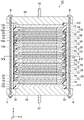
Fig. 1 is a sectional view schematically showing a power storage device of an embodiment.
Fig. 2 is an exploded perspective view schematically showing a part of the power storage device according to the embodiment.
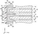
Fig. 3 is an enlarged sectional view of the 1 st resin member, the 2 nd resin member, and the welded portion.
Fig. 4 is a sectional view of the power storage device along line IV-IV of fig. 1.
Fig. 5 is a sectional view of an electricity storage device having a fusion-spliced portion according to a modification.
Fig. 6 is an enlarged sectional view of the 1 st resin member, the 2 nd resin member, and the welded portion of the modification.
Fig. 7 is a sectional view showing one step of the method for manufacturing the power storage device according to the embodiment.
Fig. 8 is a sectional view showing one step of the method for manufacturing a power storage device according to the embodiment.
Fig. 9 is a sectional view showing one step of the method for manufacturing the power storage device according to the embodiment.
Detailed Description
Hereinafter, embodiments of the present invention will be described in detail with reference to the drawings. In the description of the drawings, the same or equivalent elements will be denoted by the same reference numerals, and redundant description thereof will be omitted. In the drawings, XYZ orthogonal coordinate systems are shown as necessary.
Fig. 1 is a sectional view schematically showing a power storage device of an embodiment. Fig. 2 is an exploded perspective view schematically showing a part of the power storage device according to the embodiment. Power storage device 10 shown in fig. 1 may be a secondary battery such as a nickel-metal hydride secondary battery or a lithium ion secondary battery, or may be an electric double layer capacitor. Power storage device 10 can be mounted on a vehicle such as a forklift, a hybrid vehicle, or an electric vehicle.
The power storage device 10 includes a plurality of bipolar electrodes 12. The bipolar electrodes 12 are stacked in series with a separator 14 interposed therebetween. Each of the bipolar electrodes 12 has: a current collector 16 having a 1 st surface 16a and a 2 nd surface 16b opposite to the 1 st surface 16 a; a positive electrode layer 18 provided on the 1 st surface 16 a; and a negative electrode layer 20 provided on the 2 nd surface 16 b. Positive electrode layer 18 and negative electrode layer 20 extend along a plane (for example, XY plane) intersecting the stacking direction (hereinafter, also referred to as Z-axis direction) of the plurality of bipolar electrodes 12.
The separator 14 may be in the form of a sheet or a bag. The separator 14 is, for example, a porous film or a nonwoven fabric. The separator 14 is permeable to the electrolyte. Examples of the material of the separator 14 include polyolefins such as polyethylene and polypropylene, and polyamide-based materials such as polyimide and aramid fibers. The separator 14 reinforced with a vinylidene fluoride resin compound may be used. As the electrolyte, an alkali solution such as an aqueous solution of potassium hydroxide can be used.
The current collector 16 may be a metal foil such as a nickel foil, or may be a conductive resin member such as a conductive resin film. The thickness of the current collector 16 is, for example, 0.1 to 1000 μm. The positive electrode layer 18 contains a positive electrode active material. When power storage device 10 is a nickel-hydrogen secondary battery, the positive electrode active material is, for example, nickel hydroxide (Ni (OH) 2 ) The particles of (1). When power storage device 10 is a lithium-ion secondary battery, the positive electrode active material is, for example, a composite oxide, metallic lithium, sulfur, or the like. The negative electrode layer 20 contains a negative electrode active material. In the case where power storage device 10 is a nickel-metal hydride secondary battery, the negative electrode active material is, for example, particles of a hydrogen storage alloy. When power storage device 10 is a lithium ion secondary battery, the negative electrode active material is, for example, graphite, highly oriented graphite, mesocarbon microbeads, carbon such as hard carbon and soft carbon, an alkali metal such as lithium and sodium, a metal compound, or SiO x (x is more than or equal to 0.5 and less than or equal to 1.5), and the like, boron added carbon, and the like.
The plurality of bipolar electrodes 12 and the plurality of spacers 14 may be sandwiched between the electrodes 112 and 212 in the Z-axis direction. The electrode 112 and the electrode 212 are electrodes located on the outermost sides in the Z-axis direction. Electrode 112 includes current collector 116 and positive electrode layer 18 provided on the surface of current collector 116 on the separator 14 side. Electrode 212 includes current collector 116 and negative electrode layer 20 provided on the surface of current collector 116 on the separator 14 side. The current collector 116 has the same configuration as the current collector 16 except that it is thicker than the current collector 16 in the Z-axis direction.
The power storage device 10 includes a resin member 28 (1 st resin member) and an insulating case 30 (2 nd resin member). The resin member 28 is provided on an outer peripheral portion 161 of the current collector 16 (see fig. 3 described later). The resin members 28 adjacent in the Z-axis direction are connected to each other by a welded portion 128. The insulating case 30 is a resin case that supports the plurality of bipolar electrodes 12 via the resin member 28. The material of the insulating case 30 may be the same as or different from that of the resin member 28. The insulating case 30 is, for example, a case made of poly (p-phenylene benzobisoxazole) (Zylon (registered trademark)). The insulating housing 30 may also support the electrode 112 and the electrode 212. The insulating case 30 may be a cylindrical member that can house the plurality of bipolar electrodes 12 and the plurality of separators 14. The insulating case 30 contains an electrolyte. The resin member 28, the insulating case 30, and the weld portion 128 will be described in detail again with reference to fig. 3 to 5.
The positive electrode plate 40 and the negative electrode plate 50 are provided with through holes through which bolts B extending in the Z-axis direction pass. The through hole is disposed outside the insulating housing 30 when viewed from the Z-axis direction. The bolt B can be inserted from the positive electrode plate 40 to the negative electrode plate 50 in a state of being insulated from the positive electrode plate 40 and the negative electrode plate 50. A nut N is screwed to the tip of the bolt B. Thus, the positive electrode plate 40 and the negative electrode plate 50 can restrain the plurality of bipolar electrodes 12, the plurality of separators 14, the electrodes 112, the electrodes 212, and the insulating case 30. As a result, the insulating housing 30 can be sealed.
Fig. 3 is an enlarged sectional view of the resin member 28, the insulating case 30, and the welded portion 128. The resin member 28 is provided on at least a part of the outer peripheral portion 161 of the current collector 16. The resin member 28 may be provided in a ring shape along the entire outer peripheral portion 161. The resin member 28 is provided on at least one of the 1 st surface 16a and the 2 nd surface 16b of the current collector 16. In the example shown in fig. 3, the resin member 28 is provided on both the 1 st surface 16a and the 2 nd surface 16b of the current collector 16. The resin member 28 has: a contact surface 28a that contacts the 1 st surface 16a of the current collector 16; and a contact surface 28b that contacts the 2 nd surface 16b of the current collector 16. The resin member 28 may be provided on the end face 16c of the current collector 16, and in this case, the resin member 28 may further have a contact face 28c that contacts the end face 16c of the current collector 16. The end face 16c is a face connecting the 1 st face 16a and the 2 nd face 16 b. The contact surface 28c is a surface connecting the contact surface 28a and the contact surface 28b. The resin member 28 has a U-shaped cross section when viewed from a direction orthogonal to the outer circumferential direction of the current collector 16 (Y-axis direction in the portion shown in fig. 3), so as to cover the outer circumferential portion 161 of the current collector 16.
Examples of the material of the resin member 28 are Polystyrene (PS), polyamide (PA) 66, polycarbonate (PC), polyphenylene sulfide (PPS), polybutylene terephthalate (PBT resin), and the like. By using these materials, the resin member 28 can be provided with insulation.
The insulating case 30 is provided on the resin member 28. The insulating case 30 supports the outer peripheral portion 161 of the current collector 16 via the resin member 28. In the example shown in fig. 3, the resin member 28 is embedded in the insulating case 30 together with the outer peripheral portion 161 of the current collector 16. The insulating housing 30 has: the 1 st portion 301 located between the resin members 28 adjacent in the Z-axis direction; and a 2 nd portion 302 covering the outer side of the resin member 28. The 1 st segment 301 and the 2 nd segment 302 are alternately arranged in the Z-axis direction.
The fusion-bonding portions 128 fix the resin members 28 of the bipolar electrodes 12 adjacent to each other in the Z-axis direction to each other. The fusion-bonded portion 128 is provided on an end surface 28e located on the outer side of the resin member 28 when viewed from the Z-axis direction. The welded portion 128 extends in the Z-axis direction from the bipolar electrode 12 at one end to the bipolar electrode 12 at the other end. The weld portion 128 may be formed by irradiating the end surface 28e of the resin member 28 with ultrasonic waves, laser light, or the like, for example, or may be formed by heating the end surface 28e of the resin member 28 using a hot plate or the like, for example. The material of the weld 128 is the same as the material of the resin member 28.
Fig. 4 is a sectional view of the power storage device along line IV-IV of fig. 1. In the example shown in fig. 4, the welded portion 128 is arranged so as to surround the entire circumference of the outer peripheral portion 161 of the current collector 16 when viewed from the Z-axis direction. In this case, the welded portion 128 has a cylindrical shape. Alternatively, as shown in fig. 5, the welded portions 128 may be disposed on the respective sides of the current collector 16 having, for example, a rectangular shape when viewed from the Z-axis direction. In this case, the plurality of fusion portions 128 are arranged apart from each other. Each weld 128 is rod-shaped. The welded portion 128 is disposed at, for example, the center of each side of the current collector 16. The fusion-bonded portions 128 may be disposed at the respective apexes of the current collector 16 having a rectangular shape, for example.
In the power storage device 10 described above, the resin members 28 of the bipolar electrodes 12 adjacent in the Z-axis direction are connected to each other by the welded portion 128. Therefore, when the insulating case 30 is formed by, for example, injection molding (insert molding), even if a pressure in the lateral direction (direction within the XY plane) is applied to the bipolar electrodes 12 by, for example, a fluid of the material of the insulating case 30, positional displacement between the adjacent bipolar electrodes 12 can be suppressed. If the number of stacked bipolar electrodes 12 is large or the thickness of the bipolar electrode 12 is thin, the positional shift between adjacent bipolar electrodes tends to be large. However, even in this case, in the power storage device 10, the positional displacement between the adjacent bipolar electrodes 12 can be suppressed. By suppressing the positional shift between the adjacent bipolar electrodes, it is possible to suppress short-circuiting due to contact between the adjacent bipolar electrodes, dimensional failure of the bipolar electrodes, positional shift of the internal space in the insulating case 30, and the like.
As shown in fig. 5, if the welded portions 128 are arranged on the sides of the current collector 16 having a rectangular shape when viewed from the Z-axis direction, the effect of suppressing the positional displacement between the adjacent bipolar electrodes 12 is greater than in the case where the welded portions 128 are arranged on the vertices of the current collector 16. This is because the pressure applied to the bipolar electrode 12 is generally larger on each side than on each vertex of the current collector 16, and the positional deviation is large.
In the example described above, the 1 st resin members (resin members 28) adjacent to each other are provided separately from each other via the insulating case 30, but the 1 st resin members may be provided in contact with each other. Fig. 6 is an enlarged sectional view of the 1 st resin member (resin member 29), the 2 nd resin member (insulating housing 31), and the welded portion 129 of this modification. In the example shown in fig. 6, the respective resin members 29 of the bipolar electrodes 12 adjacent in the Z-axis direction are in contact with each other. Specifically, the resin member 29 has a contact surface 29c on the side opposite to the contact surface 29a contacting the 1 st surface 16a of the current collector 16, and a contact surface 29d on the side opposite to the contact surface 29b contacting the 2 nd surface 16b of the current collector 16. The contact surface 29c of the resin member 29 is in contact with the contact surface 29d of the resin member 29 below (in the negative Z-axis direction). The contact surface 29d of the resin member 29 is in contact with the contact surface 29c of the resin member 29 above (in the positive direction of the Z axis). The spacer 14 is located inside the resin member 29 as viewed from the Z-axis direction. In the example shown in fig. 6, the contact surface 29c of the resin member 29 is located at the center of the separator 14 below the current collector 16 on which the resin member 29 is provided, in the Z-axis direction. The contact surface 29d of the resin member 29 is located at the center of the separator 14 above the current collector 16 on which the resin member 29 is provided. The insulating housing 31 is provided in a shape matching the shape of the resin members 29, and is different from the insulating housing 30 (fig. 3) in that it does not have a portion located between the resin members 29 adjacent in the Z-axis direction.
The thickness of the resin member 29 is larger than both the thickness of the positive electrode layer 18 and the thickness of the negative electrode layer 20. When the resin member 29 is provided on both the 1 st surface 16a and the 2 nd surface 16b of the current collector 16, the thickness (length in the Z-axis direction) of the portion of the resin member 29 provided on the 1 st surface 16a of the current collector 16 is larger than the thickness of the negative electrode layer 20. The thickness of the portion of the resin member 29 provided on the 2 nd surface 16b of the current collector 16 is larger than the thickness of the positive electrode layer 18.
As described above, the thickness of resin member 29 may be larger than both the thickness of positive electrode layer 18 and the thickness of negative electrode layer 20. This ensures a space between positive electrode layer 18 and negative electrode layer 20 provided on current collector 16 of bipolar electrode 12 adjacent to each other in the stacking direction (Z-axis direction) of the plurality of bipolar electrodes 12.
The respective resin members 29 of the bipolar electrodes 12 adjacent in the Z-axis direction may also be in contact with each other. This allows the distance between the collectors 16 to be determined by the thickness of the resin member 29.
The welded portion 129 fixes the resin members 29 of the bipolar electrodes 12 adjacent in the Z-axis direction to each other. The fusion-bonded portion 129 is provided on an end surface 29e located on the outer side of the resin member 29 when viewed from the Z-axis direction. The end surface 29e connects the contact surface 29c with the contact surface 29d. The welded portion 129 extends from the bipolar electrode 12 at one end to the bipolar electrode 12 at the other end in the Z-axis direction. The welded portion 129 can be formed by the same method as the welded portion 128. The welded portion 129 may be arranged in the same manner as the welded portion 128 shown in fig. 4 or 5. The material of the weld 129 is the same as the material of the weld 128.
Next, an example of a method for manufacturing the power storage device 10 will be described with reference to fig. 7 to 9. Fig. 7 to 9 are sectional views showing one step of the method for manufacturing the power storage device according to the embodiment. Here, a case where the 1 st resin member, the 2 nd resin member, and the welded portion are the resin member 29, the insulating case 31, and the welded portion 129 shown in fig. 6 described above will be described.
(preparation Process)
First, as shown in fig. 7, a plurality of bipolar electrodes 12 and a plurality of separators 14 are prepared. Each of the plurality of bipolar electrodes 12 has a current collector 16, a positive electrode layer 18, and a negative electrode layer 20.
(step of providing the 1 st resin Member)
Next, as shown in fig. 7, the resin member 29 is provided on the outer peripheral portion 161 of the current collector 16 (see fig. 6). The resin member 29 may be provided on both surfaces of the 1 st surface 16a and the 2 nd surface 16b of the current collector 16 along the entire outer peripheral portion 161. The resin member 29 is formed, for example, by injection molding such that the resin member 29 covers the outer peripheral portion 161 of the current collector 16. Thereby, the current collector 16 and the resin member 29 are welded.
(laminating step)
Next, as shown in fig. 8, a plurality of bipolar electrodes 12 are stacked in series with a separator 14 interposed therebetween. In this lamination step, the resin members 29 of the bipolar electrodes 12 adjacent to each other in the lamination direction of the plurality of bipolar electrodes 12 are in contact with each other. The separator 14 is provided so as to be located inside the resin member 29 when viewed from the stacking direction (Z-axis direction) of the plurality of bipolar electrodes 12.
(welding Process)
Next, as shown in fig. 8, the resin members 29 of the bipolar electrodes 12 adjacent to each other in the stacking direction of the plurality of bipolar electrodes 12 are connected to each other by the fusion portion 129. That is, the adjacent resin members 29 are welded to each other. For example, the weld 129 is formed by heating the end surface 29e (see fig. 6) of the resin member 29. Thereby, the adjacent resin members 29 are fixed to each other. Alternatively, the welded portion 129 is formed by irradiating the end surface 29e of the resin member 29 with ultrasonic waves, laser light, or the like, for example.
(step of providing the No. 2 resin Member)
Next, as shown in fig. 9, the insulating case 31 is provided on the resin members 29 connected to each other by the fusion-bonded portion 129. The insulating housing 31 is formed by injection molding using a mold M, for example. First, the bipolar electrodes 12 connected to each other by the welding portion 129 are arranged in the mold M. Then, a fluid of the material of the insulating housing 31 is supplied into the mold M, and the material is cured. Thereby, the resin member 29 and the welding portion 129 are welded to the insulating case 31. The insulating case 31 supports the outer peripheral portion of the current collector 16 via the resin member 29.
Then, as described above with reference to fig. 1, the plurality of bipolar electrodes 12, the plurality of separators 14, the electrodes 112, the electrodes 212, and the insulating case 31 are sandwiched between the positive electrode plate 40 and the negative electrode plate 50. Further, the positive electrode plate 40 and the negative electrode plate 50 are applied with a restraining force using the bolt B and the nut N. Thereby, power storage device 10 is manufactured.
In the case where the 1 st resin member, the 2 nd resin member, and the welded portion are the resin member 28, the insulating case 30, and the welded portion 128 shown in fig. 3, the power storage device 10 can be manufactured by the same method as the above-described manufacturing method.
According to the above-described method for manufacturing a power storage device, the resin member 29 is provided on at least one of the 1 st surface 16a and the 2 nd surface 16b in at least a part of the outer peripheral portion 161 of the current collector 16, and then the plurality of bipolar electrodes 12 are laminated. Thus, when a plurality of bipolar electrodes 12 are stacked, the resin members 29 provided on the collectors 16 of the bipolar electrodes 12 can be used for positioning the collectors relative to each other.
The resin members 29 of the bipolar electrodes 12 adjacent to each other in the stacking direction of the plurality of bipolar electrodes 12 are connected to each other by the welding portion 129. Therefore, when the insulating case 31 is formed by, for example, injection molding, even if a lateral pressure is applied to the bipolar electrodes 12 by, for example, a fluid of the material of the insulating case 31, positional displacement between the adjacent bipolar electrodes 12 can be suppressed.
In the step of providing the resin member 29 (1 st resin member), the resin member 29 may be provided on both the 1 st surface 16a and the 2 nd surface 16 b. In the laminating step, the plurality of bipolar electrodes 12 may be laminated with the separator 14 interposed therebetween, the resin members 29 of the bipolar electrodes 12 adjacent to each other in the laminating direction of the plurality of bipolar electrodes 12 may be in contact with each other, and the separator 14 may be located inside the resin member 29 when viewed from the laminating direction of the plurality of bipolar electrodes 12. In this case, since the resin members 29 of the bipolar electrodes 12 adjacent to each other in the stacking direction are in contact with each other, the distance between the collectors 16 can be determined by the thickness of the resin members 29. Further, since the spacer 14 is positioned inside the resin member 29 when viewed from the stacking direction, the spacer 14 can also be positioned by the resin member 29.
One embodiment of the present invention has been described above, but the present invention is not limited to the above embodiment.
For example, the current collector 16 may have a polygonal or circular shape when viewed from the stacking direction of the plurality of bipolar electrodes 12.
The welded portion 128 or the welded portion 129 may be disposed on at least a part of the outer peripheral portion 161 of the current collector 16 when viewed from the stacking direction of the plurality of bipolar electrodes 12.
The fusion-bonded portion 128 may be disposed between the resin members 28 adjacent to each other in the Z-axis direction, instead of the end face 28e of the resin member 28. Similarly, the welding portion 129 may be disposed between the resin members 29 adjacent to each other in the Z-axis direction, instead of the end surface 29e of the resin member 29.
Reference numeralsDescription of the invention
10: power storage device, 12: bipolar electrode, 14: separator, 16: current collector, 16a: face 1, 16b: side 2, 18: positive electrode layer, 20: negative electrode layer, 28, 29: resin member (1 st resin member), 30, 31: insulating housing (2 nd resin member), 128, 129: weld, 161: an outer peripheral portion.
Claims (4)
1. An electricity storage device is characterized by comprising:
a plurality of bipolar electrodes which are stacked, each of the plurality of bipolar electrodes having a current collector, a positive electrode layer, and a negative electrode layer, the current collector having a 1 st surface and a 2 nd surface opposite to the 1 st surface, the positive electrode layer being provided on the 1 st surface, and the negative electrode layer being provided on the 2 nd surface;
a 1 st resin member provided on at least one of the 1 st surface and the 2 nd surface in at least a part of an outer peripheral portion of the current collector; and
a 2 nd resin member provided on the 1 st resin member and supporting the outer peripheral portion of the current collector via the 1 st resin member,
the 1 st resin members of the bipolar electrodes adjacent to each other in the stacking direction of the plurality of bipolar electrodes are connected to each other by a welded portion made of the same material as that of the 1 st resin member,
the 2 nd resin member covers the outside of the 1 st resin member,
the 1 st resin members adjacent in the laminating direction are in contact with each other,
the welded portion is provided on an end surface of the 1 st resin member on an outer side as viewed from the stacking direction, and extends from the bipolar electrode arranged at one end of the stacked body of the bipolar electrodes to the bipolar electrode at the other end of the stacked body of the bipolar electrodes,
the 2 nd resin member is welded to the 1 st resin member and the welded portion,
the 2 nd resin member is welded to the welding portion in a range from the bipolar electrode disposed at one end of the stacked body of bipolar electrodes to the bipolar electrode at the other end of the stacked body of bipolar electrodes.
2. The power storage device according to claim 1,
the welded portion is cylindrical and arranged to surround the entire circumference of the outer peripheral portion of the current collector.
3. The power storage device according to claim 1,
the welding portion is disposed on each side of the current collector having a rectangular shape when viewed from a stacking direction of the plurality of bipolar electrodes.
4. A method for manufacturing an electricity storage device having a plurality of laminated bipolar electrodes, each of the plurality of bipolar electrodes having a current collector, a positive electrode layer, and a negative electrode layer, the current collector having a 1 st surface and a 2 nd surface opposite to the 1 st surface, the positive electrode layer being provided on the 1 st surface, the negative electrode layer being provided on the 2 nd surface,
the method for manufacturing the power storage device is characterized by comprising the following steps:
a step of providing a 1 st resin member on at least one of the 1 st surface and the 2 nd surface in at least a part of an outer peripheral portion of the current collector of each of the plurality of bipolar electrodes after forming the plurality of bipolar electrodes having the positive electrode layer containing a positive electrode active material and the negative electrode layer containing a negative electrode active material;
a step of laminating the plurality of bipolar electrodes;
welding the 1 st resin members of the bipolar electrodes adjacent to each other in the stacking direction of the plurality of bipolar electrodes to each other; and
a step of forming a 2 nd resin member by injection molding, the 2 nd resin member covering the outside of the 1 st resin member after being welded to each other, the outer peripheral portion of the current collector being supported via the 1 st resin member,
in the step of welding the 1 st resin members to each other, a welded portion extending from one end of the stacked body of the bipolar electrodes to the other end of the stacked body of the bipolar electrodes in the stacking direction is formed on an outer end surface of the 1 st resin member as viewed from the stacking direction by heating the end surface of the 1 st resin member, and the 1 st resin members adjacent to each other in the stacking direction are brought into contact with each other,
in the step of forming the 2 nd resin member by injection molding, by supplying a fluid to the 2 nd resin member in a state where the plurality of bipolar electrodes in which the 1 st resin members adjacent in the stacking direction are connected to each other by the welding portion are arranged in a mold, the 2 nd resin member is welded to the 1 st resin member and the welding portion, and the 2 nd resin member is welded to the welding portion in a range from the bipolar electrode arranged at one end of the stacked body of the bipolar electrodes to the bipolar electrode arranged at the other end of the stacked body of the bipolar electrodes.
Applications Claiming Priority (3)
| Application Number | Priority Date | Filing Date | Title |
|---|---|---|---|
| JP2016-203570 | 2016-10-17 | ||
| JP2016203570A JP6705358B2 (en) | 2016-10-17 | 2016-10-17 | Method for manufacturing power storage device |
| PCT/JP2017/034103 WO2018074135A1 (en) | 2016-10-17 | 2017-09-21 | Power storage device and power storage device production method |
Publications (2)
| Publication Number | Publication Date |
|---|---|
| CN109891651A CN109891651A (en) | 2019-06-14 |
| CN109891651B true CN109891651B (en) | 2022-12-13 |
Family
ID=62019357
Family Applications (1)
| Application Number | Title | Priority Date | Filing Date |
|---|---|---|---|
| CN201780062803.1A Active CN109891651B (en) | 2016-10-17 | 2017-09-21 | Power storage device and method for manufacturing power storage device |
Country Status (5)
| Country | Link |
|---|---|
| US (1) | US11735743B2 (en) |
| JP (1) | JP6705358B2 (en) |
| CN (1) | CN109891651B (en) |
| DE (1) | DE112017005247B4 (en) |
| WO (1) | WO2018074135A1 (en) |
Families Citing this family (7)
| Publication number | Priority date | Publication date | Assignee | Title |
|---|---|---|---|---|
| CN111630680B (en) * | 2018-01-30 | 2023-01-06 | 株式会社丰田自动织机 | Power storage module and method for manufacturing power storage module |
| JP6899347B2 (en) * | 2018-03-09 | 2021-07-07 | 株式会社豊田自動織機 | Power storage device |
| JP7102911B2 (en) * | 2018-04-27 | 2022-07-20 | 株式会社豊田自動織機 | Manufacturing method of power storage module |
| JP7188062B2 (en) * | 2018-12-25 | 2022-12-13 | 株式会社豊田自動織機 | Storage module manufacturing apparatus and manufacturing method |
| US11876187B2 (en) * | 2020-08-28 | 2024-01-16 | EOS Energy Technology Holdings, LLC | Terminal assembly and battery frame member for rechargeable battery |
| WO2023218864A1 (en) * | 2022-05-11 | 2023-11-16 | 株式会社豊田自動織機 | Power storage device |
| DE102022112678B3 (en) | 2022-05-20 | 2023-08-17 | Dr. Ing. H.C. F. Porsche Aktiengesellschaft | Device and method for thermal insulation in cell stacks |
Family Cites Families (26)
| Publication number | Priority date | Publication date | Assignee | Title |
|---|---|---|---|---|
| US4275130A (en) * | 1979-09-27 | 1981-06-23 | California Institute Of Technology | Bipolar battery construction |
| JPH01195673A (en) * | 1988-01-29 | 1989-08-07 | Shin Kobe Electric Mach Co Ltd | Cell |
| US5098801A (en) * | 1990-09-12 | 1992-03-24 | General Motors Corporation | Bipolar battery and assembly method |
| CA2118866A1 (en) * | 1993-06-21 | 1994-12-22 | Clarence A. Meadows | Bipolar battery housing and method |
| US5428501A (en) * | 1993-08-13 | 1995-06-27 | Marine Mechanical Corporation | Packaging structure and method for solid electrolyte capacitors |
| JP3070474B2 (en) * | 1996-03-28 | 2000-07-31 | 日本電気株式会社 | Electric double layer capacitor and method of manufacturing the same |
| JP4122647B2 (en) * | 1999-09-09 | 2008-07-23 | 株式会社明電舎 | Electric double layer capacitor and manufacturing method thereof |
| JP2001155973A (en) | 1999-11-30 | 2001-06-08 | Meidensha Corp | Electric double-layer capacitor |
| KR100662165B1 (en) * | 2001-08-06 | 2006-12-27 | 마츠시타 덴끼 산교 가부시키가이샤 | Angular enclosed battery |
| CA2506600A1 (en) * | 2002-11-29 | 2004-06-17 | Nilar International Ab | A bipolar battery and a method for manufacturing a bipolar battery |
| JP4570863B2 (en) | 2003-10-30 | 2010-10-27 | 川崎重工業株式会社 | Bipolar plate stacked battery |
| JP4370902B2 (en) * | 2003-12-24 | 2009-11-25 | 日産自動車株式会社 | Bipolar battery and manufacturing method thereof. |
| EP1841001B1 (en) | 2004-12-10 | 2018-09-05 | Nissan Motor Co., Ltd. | Bipolar battery |
| US20090053601A1 (en) * | 2005-03-31 | 2009-02-26 | Kelley Kurtis C | Modular Bipolar Battery |
| GB0509753D0 (en) * | 2005-04-27 | 2005-06-22 | Atraverda Ltd | Electrode and manufacturing methods |
| JP2007087743A (en) * | 2005-09-21 | 2007-04-05 | Dainippon Printing Co Ltd | In-mold label and packaging container for storage battery using it |
| WO2008114738A1 (en) * | 2007-03-15 | 2008-09-25 | Gs Yuasa Corporation | Lead storage cell and battery |
| JP5458605B2 (en) * | 2009-03-05 | 2014-04-02 | 日産自動車株式会社 | Bipolar secondary battery |
| KR101218893B1 (en) * | 2009-03-05 | 2013-01-09 | 닛산 지도우샤 가부시키가이샤 | Bipolar secondary battery and method for producing the same |
| JP2011023191A (en) * | 2009-07-15 | 2011-02-03 | Nissan Motor Co Ltd | Bipolar type secondary battery |
| CN102511098B (en) * | 2010-01-29 | 2015-02-18 | 日产自动车株式会社 | Collector for bipolar lithium ion secondary battery |
| KR101209461B1 (en) * | 2010-02-01 | 2012-12-07 | 주식회사 엘지화학 | Battery Cell Assembly of Novel Structure and Battery Pack Employed with the Same |
| WO2012164642A1 (en) * | 2011-05-27 | 2012-12-06 | トヨタ自動車株式会社 | Bipolar all-solid-state battery |
| US9941546B2 (en) * | 2011-09-09 | 2018-04-10 | East Penn Manufacturing Co., Inc. | Bipolar battery and plate |
| US9685677B2 (en) * | 2011-10-24 | 2017-06-20 | Advanced Battery Concepts, LLC | Bipolar battery assembly |
| CN103959507A (en) * | 2011-10-24 | 2014-07-30 | 高级电池概念有限责任公司 | Bipolar battery assembly |
-
2016
- 2016-10-17 JP JP2016203570A patent/JP6705358B2/en active Active
-
2017
- 2017-09-21 CN CN201780062803.1A patent/CN109891651B/en active Active
- 2017-09-21 WO PCT/JP2017/034103 patent/WO2018074135A1/en active Application Filing
- 2017-09-21 US US16/325,488 patent/US11735743B2/en active Active
- 2017-09-21 DE DE112017005247.5T patent/DE112017005247B4/en active Active
Also Published As
| Publication number | Publication date |
|---|---|
| US11735743B2 (en) | 2023-08-22 |
| DE112017005247B4 (en) | 2023-05-11 |
| JP2018067381A (en) | 2018-04-26 |
| JP6705358B2 (en) | 2020-06-03 |
| CN109891651A (en) | 2019-06-14 |
| US20190260034A1 (en) | 2019-08-22 |
| DE112017005247T5 (en) | 2019-07-11 |
| WO2018074135A1 (en) | 2018-04-26 |
Similar Documents
| Publication | Publication Date | Title |
|---|---|---|
| CN109891651B (en) | Power storage device and method for manufacturing power storage device | |
| JP6780345B2 (en) | Power storage device and manufacturing method of power storage device | |
| JP6586969B2 (en) | Power storage module | |
| US9299964B2 (en) | Energy storage element | |
| KR20130113301A (en) | Battery cell of stair-like structure | |
| JP6838640B2 (en) | Power storage device | |
| EP2683010B1 (en) | Secondary battery comprising two electrode assemblies | |
| CN110770956A (en) | Stacked prismatic architecture for electrochemical cells | |
| JP2009087613A (en) | Square battery | |
| KR20210041503A (en) | Electrochemical cell | |
| JP2018049793A (en) | Power storage device | |
| JP2015082386A (en) | Storage battery | |
| US20140255761A1 (en) | Battery cell, manufacturing method thereof, and battery module including the same | |
| JP5692359B2 (en) | Power storage device and method for manufacturing power storage device | |
| KR101918412B1 (en) | Stacked battery | |
| US20220247023A1 (en) | Power storage device | |
| WO2018123502A1 (en) | Power storage module and manufacturing method for power storage module | |
| JP2013232374A (en) | Power storage device | |
| JP2019061881A (en) | Power storage element | |
| JP2018018666A (en) | Power storage device and method for manufacturing power storage device | |
| JP2019079614A (en) | Power storage module, and method for manufacturing power storage module | |
| JP2019061892A (en) | Power storage element | |
| JP2018067382A (en) | Power storage device | |
| JP2018049794A (en) | Power storage device, and method for manufacturing the same | |
| CN107591555B (en) | Secondary battery |
Legal Events
| Date | Code | Title | Description |
|---|---|---|---|
| PB01 | Publication | ||
| PB01 | Publication | ||
| SE01 | Entry into force of request for substantive examination | ||
| SE01 | Entry into force of request for substantive examination | ||
| GR01 | Patent grant | ||
| GR01 | Patent grant |