Disclosure of Invention
In view of the above, embodiments of the present invention provide a shift register, a gate driving circuit, a display panel and a display device, so as to solve the problem of multiple outputs of the shift register caused by insufficient discharge of pull-up nodes in the conventional shift register.
Accordingly, an embodiment of the present invention provides a shift register, including: a reset module having a first terminal, a second terminal, and a reset control terminal, the first terminal of the reset module being connected to a first reference voltage signal terminal, the second terminal of the reset module being connected to a pull-up node of the shift register, the reset module being configured to: when a reset signal is loaded to the reset control end, resetting the potential of the pull-up node to a first reference voltage; and
a first capacitor having a first electrode and a second electrode disposed opposite to each other, the first electrode of the first capacitor being connected to the reset control terminal, and the first capacitor being configured to: a first electrode of the first capacitor can be loaded with a first voltage signal, and a second electrode of the first capacitor can be loaded with a second voltage signal;
the first voltage signal and the second voltage signal have the same waveform, and the starting edge of the first voltage signal is earlier than that of the second voltage signal.
In a possible implementation manner, in the shift register provided in an embodiment of the present invention, the reset module includes: a first transistor;
the grid electrode of the first transistor is connected with the first voltage signal end and the first electrode of the first capacitor, the first pole of the first transistor is connected with the first reference voltage signal end, and the second pole of the first transistor is connected with the pull-up node.
In a possible implementation manner, the shift register provided in the embodiment of the present invention further includes: a second transistor;
the grid electrode of the second transistor and the first pole of the second transistor are both connected with an input signal end, and the second pole of the second transistor is connected with the pull-up node;
the second transistor is configured to: and providing the signal of the input signal terminal to the pull-up node under the control of the input signal terminal.
In a possible implementation manner, the shift register provided in the embodiment of the present invention further includes: a third transistor;
the grid electrode of the third transistor is connected with the pull-up node, the first pole of the third transistor is connected with the clock signal end, and the second pole of the third transistor is connected with the first signal output end;
the third transistor is configured to: and providing the signal of the clock signal end to the first signal output end under the control of the electric potential of the pull-up node.
In a possible implementation manner, the shift register provided in the embodiment of the present invention further includes: a fourth transistor;
the grid electrode of the fourth transistor is connected with the pull-up node, the first pole of the fourth transistor is connected with the clock signal end, and the second pole of the fourth transistor is connected with the second signal output end;
the fourth transistor is configured to: and providing the signal of the clock signal end to the second signal output end under the control of the pull-up node.
In a possible implementation manner, the shift register provided in the embodiment of the present invention further includes: a second capacitor;
the second capacitor has a first electrode and a second electrode disposed opposite to each other, the first electrode of the second capacitor is connected to the pull-up node, the second pole of the second capacitor is connected to the first signal output terminal, and the second capacitor is configured to: and keeping the voltage difference between the pull-up node and the first signal output terminal stable.
In a possible implementation manner, in the shift register provided in the embodiment of the present invention, all the transistors are N-type transistors, or all the transistors are P-type transistors.
Correspondingly, the embodiment of the invention also provides a gate drive circuit, which comprises any one of the shift registers provided by the embodiment of the invention;
the first voltage signal end of the nth stage shift register is connected with the second signal output end of the (n +1) th stage shift register;
and the second voltage signal end of the nth stage shift register is connected with the second signal output end of the (n +2) th stage shift register.
Correspondingly, the embodiment of the invention also provides a display panel which comprises the gate driving circuit provided by the embodiment of the invention.
Correspondingly, the embodiment of the invention also provides a display device which comprises the display panel provided by the embodiment of the invention.
The invention has the following beneficial effects:
the shift register, the gate driving circuit, the display panel and the display device provided by the embodiment of the invention comprise: a reset module and a first capacitor; wherein the reset module is configured to: when the reset signal is loaded to the reset control end, the potential of the pull-up node is reset to the first reference voltage, the reset control end of the reset module is provided with a first capacitor to keep the potential of the reset control end, and the potential of the reset control end is improved through the input of the first voltage signal and the second voltage signal, so that the sufficient discharge of the pull-up node is realized, the problem of multiple output of the shift register is relieved, and the normal display of the display panel is ensured.
Detailed Description
In order to make the objects, technical solutions and advantages of the present invention clearer, specific embodiments of a shift register, a gate driver circuit and a display device according to an embodiment of the present invention are described in detail below with reference to the accompanying drawings. It should be understood that the preferred embodiments described below are only for illustrating and explaining the present invention and are not to be used for limiting the present invention. And the embodiments and features of the embodiments in the present application may be combined with each other without conflict.
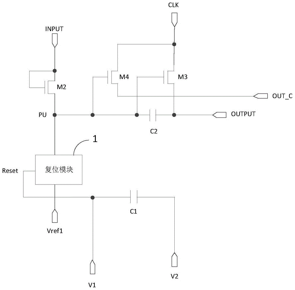
An embodiment of the present invention provides a shift register, as shown in fig. 1, including: the Reset module 1, the Reset module 1 having a first terminal, a second terminal and a Reset control terminal Reset, the first terminal of the Reset module 1 being connected to a first reference voltage signal terminal Vref1, the second terminal of the Reset module 1 being connected to a pull-up node PU of the shift register, the Reset module 1 being configured to: when a Reset signal is loaded to a Reset control end Reset, resetting the potential of a pull-up node PU to a first reference voltage; and
a first capacitor C1, the first capacitor C1 having a first electrode and a second electrode disposed opposite to each other, the first electrode of the first capacitor C1 being connected to the Reset control terminal Reset, and the first capacitor C1 being configured to: a first electrode of the first capacitor C1 can be loaded with a first voltage signal V1, and a second electrode of the first capacitor C1 can be loaded with a second voltage signal V2;
the first voltage signal V1 and the second voltage signal V2 have the same waveform, and the start edge of the first voltage signal V1 is earlier than the start edge of the second voltage signal V2.
It should be noted that, in the shift register provided in the embodiment of the present invention, the first reference voltage signal terminal is configured to provide a first reference voltage, the first voltage signal terminal is configured to provide a first voltage signal, and the second voltage signal terminal is configured to provide a second voltage signal; the pull-up node is connected with the control end of a module or a transistor for controlling the output of each signal output end of the shift register.
In the prior art, a reset control end of a shift register is directly connected with an output end of a next-stage shift register, when the next-stage shift register has a signal output, a pull-up node of the shift register is discharged, but due to the fact that channel current is low under the low-temperature condition, a reset module cannot completely discharge the pull-up node, the pull-up node has residual voltage, and the shift register has the phenomenon of multiple output.
The shift register provided by the embodiment of the invention comprises: a reset module and a first capacitor; wherein the reset module is configured to: when the reset signal is loaded to the reset control end, the potential of the pull-up node is reset to the first reference voltage, the reset control end of the reset module is provided with a first capacitor to keep the potential of the reset control end, and the potential of the reset control end is improved through the input of the first voltage signal and the second voltage signal, so that the sufficient discharge of the pull-up node is realized, the problem of multiple output of the shift register is relieved, and the normal display of the display panel is ensured.
It is to be noted that, in the shift register provided by the embodiment of the present invention, the phase of the first voltage signal provided by the first voltage signal terminal is the same as the phase of the second voltage signal provided by the second voltage signal terminal, and the start edge of the first voltage signal is earlier than the start edge of the second voltage signal (i.e. the time that the first voltage signal terminal provides the signal is earlier than the time that the second voltage signal terminal provides the signal). In specific implementation, the time for providing the signal by the first voltage signal end is earlier than the time for providing the signal by the second voltage signal end, and there are two situations, wherein one situation is that the first voltage signal end provides the signal first, and the second voltage signal end provides the signal again when the signal of the first voltage signal end is provided, so as to improve the voltage of the reset control end; in another case, the first voltage signal terminal first provides a signal, and the second voltage signal terminal starts to provide a signal when the first voltage signal terminal does not finish providing the signal, that is, the first voltage signal terminal and the second voltage signal terminal simultaneously provide signals within a preset time, so as to increase the voltage of the reset control terminal. The voltage of the reset control end can be longer than the time of a signal of the reset control end in the prior art and higher than the voltage by the arrangement of the two conditions, so that the pull-up node is better discharged. The two conditions are selected according to actual requirements, and are not specifically limited herein.
In practical implementation, in the shift register provided in the embodiment of the present invention, the first voltage signal terminal of the shift register (n) in this stage is connected to the output terminal of the next shift register (n +1), and the second voltage signal terminal is connected to the output terminal of the next shift register (n +2), so that the signal provided by the first voltage signal terminal is earlier than the signal provided by the second voltage signal terminal. When the time that the first voltage signal end provides signals to the reset control end and the time that the second voltage signal end provides signals to the reset control end coincide, the next-stage shift register and the next-stage shift register can be charged, and the high-pixel display panel can achieve better display.
Specifically, in the shift register provided in the embodiment of the present invention, when the first voltage signal terminal inputs the first voltage signal, the first voltage signal is provided to the reset control terminal to discharge the pull-up node, and the first voltage signal of the first voltage signal terminal also charges the first capacitor, where the reset control terminal has the first voltage; and then a second voltage signal is input into the second voltage signal end, the voltage of the reset control end is increased due to the bootstrap action of the first capacitor, namely the reset control end has the second voltage, the discharge of the pull-up node is sufficient by increasing the voltage of the reset control end and prolonging the time, and the problem of multiple output of the shift register caused by insufficient discharge of the pull-up node due to low temperature and small channel current is solved.
The shift register in the above embodiment may be used to improve the problem of insufficient noise reduction of the pull-up node at low temperature, and may also be used to solve the problem of insufficient noise reduction of the pull-up node caused by other reasons. If the use temperature of a gate drive circuit on a vehicle-mounted product is relatively wide (-40-90 ℃), wherein the problem of insufficient noise reduction of a pull-up node is easily caused at-40 ℃, the shift register provided by the embodiment of the invention can ensure that the noise of the pull-up node is fully released, and normal display is ensured.
The present invention will be described in detail with reference to specific examples. It should be noted that the present embodiment is for better explaining the present invention, but not limiting the present invention.
Optionally, in the shift register provided in the embodiment of the present invention, as shown in fig. 2, the reset module 1 includes: a first transistor M1;
a gate of the first transistor M1 is connected to the first voltage signal terminal V1 and a first electrode of the first capacitor C1, a first pole of the first transistor M1 is connected to the first reference voltage signal terminal Vref1, and a second pole of the first transistor is connected to the pull-up node PU.
Specifically, in the shift register provided in the embodiment of the present invention, the channel current of the first transistor is related to the gate voltage and the threshold voltage of the first transistor, and since the threshold voltage of one transistor belongs to the attribute of the transistor, the channel current of the first transistor can be increased by increasing the gate voltage of the first transistor, so that the pull-up node is more sufficiently discharged.
The above is only an example of the specific structure of the reset module in the shift register, and in the specific implementation, the specific structure of the reset module is not limited to the above structure provided by the embodiment of the present invention, and may be other structures known to those skilled in the art, and is not limited herein.
Optionally, in the shift register provided in the embodiment of the present invention, as shown in fig. 2, the shift register further includes: a second transistor M2;
the grid of the second transistor M2 and the first pole of the second transistor M2 are both connected to the INPUT signal terminal INPUT, and the second pole of the second transistor M2 is connected to the pull-up node PU;
the second transistor M2 is configured to: the signal of the INPUT signal terminal INPUT is supplied to the pull-up node PU under the control of the INPUT signal terminal INPUT.
Specifically, in the shift register provided by the embodiment of the present invention, the second transistor supplies a signal of the input signal terminal to the pull-up node under the control of the input signal terminal, that is, charges the pull-up node to control the outputs of the third transistor and the fourth transistor.
Optionally, in the shift register provided in the embodiment of the present invention, as shown in fig. 2, the shift register further includes: a third transistor M3;
a gate of the third transistor M3 is coupled to the pull-up node PU, a first pole of the third transistor M3 is coupled to the clock signal terminal CLK, and a second pole of the third transistor M3 is coupled to the first signal OUTPUT terminal OUTPUT;
the third transistor M3 is configured to: the signal of the clock signal terminal CLK is supplied to the first signal OUTPUT terminal OUTPUT under the control of the potential of the pull-up node PU.
Specifically, in the shift register provided in the embodiment of the present invention, the third transistor provides a clock signal at a clock signal end to the first signal output end under the control of the potential of the pull-up node, so as to input a driving scan signal to a corresponding gate line in the display panel, so that a pixel corresponding to the display panel performs display.
Optionally, in the shift register provided in the embodiment of the present invention, as shown in fig. 2, the shift register further includes: a fourth transistor M4;
a gate of the fourth transistor M4 is connected to the pull-up node PU, a first pole of the fourth transistor M4 is connected to the clock signal terminal CLK, and a second pole of the fourth transistor M4 is connected to the second signal output terminal OUT _ C;
the fourth transistor M4 is configured to: the signal of the clock signal terminal CLK is supplied to the second signal output terminal OUT _ C under the control of the pull-up node PU.
Specifically, in the shift register provided in the embodiment of the present invention, the fourth transistor provides a clock signal at a clock signal end to the second signal output end under the control of the potential of the pull-up node, and the fourth transistor is cascaded with the shift registers of other stages through the second signal output end, so as to ensure normal cascaded signal transmission of the entire gate driving circuit.
It should be noted that, in the shift register provided in the embodiment of the present invention, the first signal output terminal is used to provide a driving scanning signal to a corresponding gate line in the display panel, and the second signal output terminal is used to cascade with other shift registers, so that the reset of other shift registers can be prevented from being affected when the first signal output terminal of a certain stage of shift register outputs an abnormal output.
Optionally, in the shift register provided in the embodiment of the present invention, as shown in fig. 2, the shift register further includes: a second capacitance C2;
the second capacitor C2 has first and second electrodes disposed opposite to each other, the first electrode of the second capacitor C2 is connected to the pull-up node PU, the second pole of the second capacitor C2 is connected to the first signal OUTPUT terminal OUTPUT, and the second capacitor C2 is configured to: the voltage difference between the pull-up node PU and the first signal OUTPUT terminal OUTPUT is kept stable.
Optionally, in the shift register provided in the embodiment of the present invention, all the transistors are N-type transistors, or all the transistors are P-type transistors. The N-type switch transistor is switched on under the action of a high potential signal and is switched off under the action of a low potential signal; the P-type switching transistor is turned off under the action of a high potential signal and turned on under the action of a low potential signal.
The transistors mentioned in the above embodiments of the present invention may be Thin Film Transistors (TFTs) or Metal Oxide Semiconductor field effect transistors (MOS), unless otherwise specified, and are not limited herein. In a specific implementation, the control electrode of each transistor is used as the gate thereof, and according to the type of the transistor and the input signal, the first electrode can be used as the source, and the second electrode can be used as the drain; or the first pole is used as the drain and the second pole is used as the source, which is not specifically distinguished here.
In practical implementation, in the shift register provided by the present invention, as shown in fig. 3, the shift register includes not only the first transistor M1, the second transistor M2, the third transistor M3, the fourth transistor M4, the first capacitor C1 and the second capacitor C2, but also the first pull-down node control module (M5, M6, M8 and M9) and the second pull-down node control module (M5-1, M6-1, M8-1 and M9-1) for controlling the pull-down node PD, the pull-up node noise reduction module (M10 and M10-1), the first signal output terminal noise reduction module (M11 and M11-1) and the second output terminal noise reduction module (M12 and M12-1), wherein the first pull-down node control module, the second pull-down node control module, the pull-up node noise reduction module, the first signal output terminal noise reduction module and the second output terminal noise reduction module are all in the existing noise reduction process, and will not be described in detail herein.
Based on the same inventive concept, the embodiment of the invention further provides a gate driving circuit, which comprises the shift register provided by any one of the embodiments;
the first voltage signal end of the nth stage shift register is connected with the second signal output end of the (n +1) th stage shift register;
and the second voltage signal end of the nth stage shift register is connected with the second signal output end of the (n +2) th stage shift register.
Examples
The process of charging and discharging the pull-up node PU will be described in detail with reference to the shift register shown in fig. 2 and the timing diagram shown in fig. 4, wherein all the transistors are N-type transistors, and the first reference voltage signal terminal Vref1 is a low level signal.
First, the INPUT signal terminal INPUT of the nth stage shift register is a high level signal, the second transistor M2 is turned on to precharge the pull-up node PU, after the precharge of the pull-up node PU is completed, the clock signal from the clock signal terminal CLK is provided to the first signal OUTPUT terminal OUTPUT, the potential of the pull-up node PU is further pulled up by the bootstrap action of the second capacitor C2, and the clock signal from the clock signal terminal CLK is INPUT to the first signal OUTPUT terminal OUTPUT and the second signal OUTPUT terminal OUT _ C (n).
Next, the signal of the second signal output terminal OUT _ C (n +1) of the n +1 th stage shift register is supplied to the first voltage signal terminal V1 of the nth stage shift register, thereby raising the potential of the gate of the first transistor M1 of the nth stage shift register (i.e., the Reset control terminal Reset of the nth stage shift register) to discharge the pull-up node PU while charging the first capacitor C1; when the second signal output terminal OUT _ C (n +2) of the n +2 th stage shift register supplies a signal to the second voltage signal terminal V2 of the nth stage shift register, the voltage of the gate of the first transistor M1 (i.e., the Reset control terminal Reset of the nth stage shift register) is further increased due to the bootstrap action of the first capacitor C1 to increase the channel current of the first transistor M1, and the pull-up node PU is sufficiently discharged to prevent the nth stage shift register from having a phenomenon of multiple outputs.
Wherein, CLK (n), CLK (n +1), and CLK (n +2) are clock signals supplied from clock signal lines connected to clock signal terminals of the nth stage shift register, the n +1 th stage shift register, and the n +2 th stage shift register, respectively.
Based on the same inventive concept, embodiments of the present invention further provide a display panel, including any one of the gate driving circuits provided in embodiments of the present invention.
Based on the same inventive concept, the embodiment of the invention also provides a display device, which comprises the display panel provided by the embodiment of the invention. The display device may be: the display panel of any product with a display function, such as a mobile phone, a tablet personal computer, a television, a display, a notebook computer, a digital photo frame, a navigator and the like. The implementation of the display device can be seen in the embodiments of the gate driving circuit, and repeated descriptions are omitted.
The shift register, the gate driving circuit, the display panel and the display device provided by the embodiment of the invention comprise: a reset module and a first capacitor; wherein the reset module is configured to: when the reset signal is loaded to the reset control end, the potential of the pull-up node is reset to the first reference voltage, the reset control end of the reset module is provided with a first capacitor to keep the potential of the reset control end, and the potential of the reset control end is improved through the input of the first voltage signal and the second voltage signal, so that the sufficient discharge of the pull-up node is realized, the problem of multiple output of the shift register is relieved, and the normal display of the display panel is ensured.
It will be apparent to those skilled in the art that various changes and modifications may be made in the present invention without departing from the spirit and scope of the invention. Thus, if such modifications and variations of the present invention fall within the scope of the claims of the present invention and their equivalents, the present invention is also intended to include such modifications and variations.