Detailed Description
The term "device" will be used herein to refer to a "microfluidic or millifluidic device" according to the present invention. In the same way, the term "main channel" will be used herein to refer to a "main microchannel or millimeter channel" according to the invention.
Dielectric material
The support of the device according to the invention is at least partially made of a dielectric material (which is thus solid) in order to insulate the device (since a high voltage electric field is generated inside the support between electrodes embedded in said dielectric material), and to allow the formation of a plasma in the gas bubbles by means of a Dielectric Barrier Discharge (DBD). This is why the main channel is present in the dielectric material.
The dielectric material used in the present invention may be any material that is well known for its dielectric properties. However, the dielectric material is advantageously impermeable to gases and liquids that need to flow through the channels comprised in the support. Furthermore, the dielectric material should advantageously also be able to form a support comprising at least a channel (main channel) and a buried electrode.
The dielectric material may thus be a UV-cured polymer (i.e., a polymer obtained from photopolymerization of a monomer or prepolymer), such as a polymer obtained by photopolymerization of a mercapto-ene based resin (e.g., Norland Optical
(NOA), such as NOA-81 or NOA-61, preferably NOA-81)), poly (tetramethylene succinate) (PTMS), cyclic olefin copolymer (COC, such as a copolymer of ethylene and norbornene or tetracyclododecene), glass, or combinations thereof.
Main channel
The support comprises micro-or millimeter-channels, which are preferably linear micro-or millimeter-channels.
In the present invention, "microchannel or millimeter channel" means a channel having a cross-sectional dimension (particularly, width) in the range of micrometers or millimeters. Thus, a microchannel will be a channel having a cross-sectional dimension (particularly width) in the micrometer range, while a millimeter channel will be a channel having a cross-sectional dimension (particularly width) in the millimeter range. Typically, the width and depth of the micro-or millimetre channels will be between 1 μm and 10mm, in particular between 10 μm and 5mm, preferably between 100 μm and 3 mm.
The width of the main microchannel will more particularly be between 1 and 1000 μm, in particular between 10 and 500 μm, preferably between 100 and 300 μm, while the depth of the main microchannel will more particularly be between 10 μm and 2mm, in particular between 50 μm and 1mm, preferably between 70 and 200 μm. The width of the main millimeter-wave channel will more particularly be between 1mm and 10mm, in particular between 1mm and 5mm, preferably between 1mm and 3mm, while the depth of the main millimeter-wave channel will more particularly be between 10 μm and 2mm, in particular between 50 μm and 2mm, preferably between 100 and 2 mm.
However the length of the micro-or millimetre channels may be in the range of centimetres or decimetres.
Electrode for electrochemical cell
The device according to the invention comprises at least one ground electrode and at least one high voltage electrode.
"ground electrode" (also referred to as ground pole) means an electrode connected to ground.
By "high voltage electrode" is meant an electrode connected to a high voltage power supply, advantageously a high voltage power supply between 1kV and 30kV, in particular between 5kV and 20kV, preferably between 10kV and 15 kV.
The ground electrode and the high voltage electrode are made of an electrically conductive material, such as indium (In), tin (Sn), copper (Cu), gold (Au) or oxides and/or alloys thereof, In particular Indium Tin Oxide (ITO), copper (Cu), gold (Au) or indium tin (In-Sn) alloys, more In particular indium tin alloys. The ground electrode and the high voltage electrode may be made of the same or different conductive materials.
The ground electrode may be constituted by one or several ground electrodes extending along the main channel. Each ground electrode may have various forms. It may be a planar electrode, an electrode with a meandering form, a planar electrode with fins and/or tips extending towards the main channel, etc.
In the same way, the hv electrode may be constituted by one or several hv electrodes extending along the main channel. Each ground electrode may have various forms. It may be a planar electrode, an electrode with a meandering form, a planar electrode with fins and/or tips extending towards the main channel, etc. In particular, it is a planar electrode.
The ground electrode and the high voltage electrode may have the same or different forms.
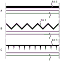
Fig. 2A-2B schematically illustrate top views of a high voltage electrode 5 or a ground electrode 4 extending along a primary microchannel or millimeter-channel 3, the electrodes 5 or 4 having various possible forms, according to various embodiments of the invention. Thus, fig. 2A shows a planar electrode 5 or 4 extending along the main channel 3, fig. 2B shows a meandering electrode 5 or 4 extending along the main channel 3, and fig. 2C shows a planar electrode 5 or 4 with fins and/or tips extending towards the main channel 3. However other forms are contemplated.
According to a particular embodiment, there is one ground electrode (in particular a planar ground electrode) and one or several high voltage electrodes extending along the main channel.
According to another embodiment, there is one high voltage electrode (in particular a planar high voltage electrode) and one or several ground electrodes extending along the main channel.
According to a preferred embodiment, there is one ground electrode and one high voltage electrode extending along the main channel. According to a most preferred embodiment, the ground electrode and the high voltage electrode are planar electrodes.
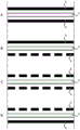
Fig. 3A to 3D schematically show various embodiments according to the invention of the high and ground voltage electrodes 5 and 4 and the main channel 3. Thus, fig. 3A shows an embodiment where there is one high voltage electrode 5 and one ground electrode 4 extending along the main channel 3, fig. 3B shows an embodiment where there is one high voltage electrode 5 and several ground electrodes 4 extending along the main channel 3, fig. 3C shows an embodiment where there are several high voltage electrodes 5 and several ground electrodes 4 extending along the main channel 3, and fig. 3D shows an embodiment where there are several high voltage electrodes 5 and one ground electrode 4 extending along the main channel 3. However other embodiments are contemplated. In these figures, the electrodes 4 and 5 are shown as planar electrodes for practical reasons. However, other forms are contemplated, such as those represented in fig. 2.
Advantageously, the distance between the high voltage electrode and the ground electrode will be between 500 μm and 10mm, in particular between 500 μm and 5mm, preferably between 500 and 2 mm. Smaller distances are preferred, in particular between 500 μm and 1000 μm, in order to achieve a lower breakdown voltage (which is less energy consuming). The distance also depends on the width of the main channel present between the two electrodes.
Advantageously, the distance between the high voltage electrode or the ground electrode and the main channel will be between 10 μm and 2mm, in particular between 50 μm and 1mm, preferably between 100 μm and 1 mm.
Advantageously, the distance over which the hv electrode extends along the main microchannel or millichannel 3 is at least 1cm, in particular at least 2cm, for example between 1cm and 10cm, in particular between 2cm and 5 cm.
Advantageously, the ground electrode extends along the main microchannel or millichannel 3 for a distance of at least 1cm, in particular at least 2cm, for example between 1cm and 10cm, in particular between 2cm and 5 cm.
Microfluidic or microfluidic devices
The support of the device comprises a first inlet and a second inlet adapted to be connected to a first reservoir and a second reservoir, respectively, said first reservoir being adapted to contain a gas and said second reservoir being adapted to contain a liquid. The support further comprises an outlet adapted to be connected to a receiving vessel adapted to contain a gas and/or a liquid.
Thus, the device according to the invention further comprises a first reservoir and a second reservoir; said first reservoir is adapted to contain a gas (more particularly a pressurised gas) so as to enable the gas to be injected from the first reservoir into the support and to flow through the main channel; the second reservoir is adapted to contain a liquid (more particularly, a pressurized liquid) so that the liquid can be injected from the second reservoir into the support and flow through the primary channel. The device further comprises a receiving container adapted to contain a gas and/or liquid, thereby receiving the gas and/or liquid obtained at the end of the main channel.
The outlet of the support enables the gas and/or liquid obtained at the end of the main channel to exit outside the support. Thus, the outlet is connected to the main channel by any means that enables gas and liquid to flow from the main channel to the outlet; for example through an outlet channel (which may be of any shape and size and which is advantageously a microchannel or a microchannel).
The inlet of the support enables gas and liquid to enter the support from the corresponding reservoir. The inlet is then connected to the main channel in such a way that gas and liquid can flow up to the main channel, in which gas bubbles are formed in the liquid.
Various methods can be used to form gas bubbles in a liquid. For example, pulsed pressure may be applied to the gas to form gas bubbles in the liquid. A flow focusing design may also be used to generate gas bubbles in a liquid as described by Garstecki et al [4 ]. This means that the gas flow is sheared by two opposing liquid flows and thus means the second liquid inlet. This second embodiment using a flow-focusing design is preferred because it enables bubbles to be formed with controlled shape (roughly spherical bubbles), controlled size, and controlled flow-through velocity.
Advantageously, the two inlets 21a and 21b are connected to the two injection channels 6a and 6b, respectively (advantageously micro-channels or millimetric channels). The two injection channels 6a and 6b are then connected to the main microchannel or millimeter channel 3.
In the present invention, an "injection channel" means a channel that enables a liquid or gas to enter the microfluidic or microfluidic device 1 through one of its inlets. The liquid or gas thus entering can then reach the main micro-or milli-channel 3.
Two injection channels 6a and 6b will be connected to the two inlets 21a and 21b and to the main micro-or milli-channel 3, ensuring that liquid and gas enter the micro-or milli-fluidic device 1 and gas bubbles are formed in the liquid (especially at a controlled size and frequency).
According to a first embodiment, the support comprises:
a first injection channel, advantageously a microchannel or a millimeter channel, and connecting the first inlet to the main channel, an
A second injection channel, advantageously a microchannel or a millimeter channel, and connecting the second inlet to the main channel,
wherein the first and second channels meet the main channel at a junction, and
wherein the secondary channel and the primary channel are advantageously continuations of each other.
This first embodiment can be used to form gas bubbles in the liquid at the junction of the first channel, the second channel and the main channel.
Such an embodiment with point-to-face electrodes is schematically shown in fig. 1A. The support 2 made of dielectric material then comprises:
a first inlet 21a adapted to be connected to a first reservoir containing a gas,
a second inlet 21b adapted to be connected to a second reservoir containing a liquid,
an outlet 22 adapted to be connected to a receiving vessel containing a gas and/or a liquid,
a main microchannel or millichannel 3 enabling the liquid and gas to flow from the inlets 21a and 21b towards the outlet 22,
one or several ground electrodes 4 (represented in fig. 1A as a planar ground electrode) embedded in the dielectric material and extending along the main microchannel or millimeter-channel 3,
one or several high voltage electrodes 5 (represented in fig. 1A as one meandering high voltage electrode) embedded in the dielectric material and extending along the main micro-or millimeter-wave channel 3,
a first injection channel 6a, advantageously a microchannel or a millichannel, and connecting the first inlet 21a to the main channel 3,
a second injection channel 6b, advantageously a microchannel or a millimeter channel, and connecting the second inlet 21b to the main channel 3, an
An outlet channel 7, advantageously a microchannel or a microchannel, and connecting the outlet 22 to the main channel 3.
According to a second embodiment, the support further comprises a third inlet adapted to be connected to the second reservoir or a third reservoir adapted to contain a liquid, in particular for enabling the generation of gas bubbles by a flow-concentrating design. Thus, according to this preferred embodiment, the device can further comprise a third reservoir adapted to contain a liquid (more particularly, a pressurized liquid).
In this second embodiment, the support will advantageously comprise:
a first injection channel, advantageously a microchannel or a millimeter channel, and connecting the first inlet to the main channel,
a second injection channel, advantageously a microchannel or a millimeter channel, and connecting the second inlet to the main channel, an
A third injection channel, advantageously a microchannel or a millimeter channel, and connecting the third inlet to the main channel,
wherein the first, second and third injection passages merge with the main passage at a junction, and
wherein, at the junction, each of the second and third injection channels extends perpendicularly with respect to the first injection channel, the second and third injection channels being continuations of each other. Advantageously, the first injection channel and the main channel are continuations of each other.
Such an embodiment with facing electrodes is schematically shown in fig. 1B. The support 2 made of dielectric material then comprises:
a first inlet 21a adapted to be connected to a first reservoir containing a gas,
a second inlet 21b adapted to be connected to a second reservoir containing a liquid,
a third inlet 21c adapted to be connected to the second reservoir or a third reservoir containing a liquid,
an outlet 22 adapted to be connected to a receiving vessel containing a gas and/or a liquid,
a main microchannel or millichannel 3 enabling liquid and gas to flow from the inlets 21a, 21b and 21c towards the outlet 22,
one or several ground electrodes 4 (represented in fig. 1B as a planar ground electrode) embedded in the dielectric material and extending along the main microchannel or millimeter-channel 3,
one or several high voltage electrodes 5 (represented in fig. 1B as one planar high voltage electrode) embedded in the dielectric material and extending along the main micro-or millimeter-channel 3,
a first injection channel 6a, advantageously a microchannel or a millichannel, and connecting the first inlet 21a to the main channel 3,
a second injection channel 6b, advantageously a microchannel or a millichannel, and connecting the second inlet 21b to the main channel 3,
a third injection channel 6c, advantageously a microchannel or a millimeter channel, and connecting the third inlet 21c to the main channel 3, an
An outlet channel 7, advantageously a microchannel or a microchannel, and connecting the outlet 22 to the main channel 3.
FIG. 1C further shows a second embodiment (flow concentration design) [4] according to the above]And the three injection channels 6a, 6b and 6c with the main channel 3. In fact, to better control the size of the bubbles at this junction, the width (W) of the main channel at the junction where the gas bubbles are formedo) Advantageously not greater than (in particular less than) the width (W) of the main channel (where the gas bubbles flow into the liquid) after the junctionout)。
Advantageously, the microfluidic or millifluidic device 1 will further comprise a high voltage power supply connected to the ground electrode 4 and the high voltage electrode 5.
The high voltage power supply is used to apply a high voltage between the ground electrode 4 and the high voltage electrode 5 and to generate an electric field inside the main micro-or millimeter-channel 3. In particular, the high voltage power supply must be able to supply sufficient energy to the gas bubbles to be circulated inside the main micro-or millimeter-channel 3, so as to generate a Dielectric Barrier Discharge (DBD) with suitable energy and to generate a plasma in the bubbles in a continuous manner.
The high voltage supplied by the high voltage power supply is typically comprised between 1kV and 30kV, in particular between 5kV and 20kV, preferably between 10kV and 15 kV.
According to a first embodiment, the high voltage power supply is a variable high voltage power supply, i.e. provides a variable high voltage. The high voltage supplied by the high voltage power supply will more particularly be a sinusoidal high voltage, the frequency of which is advantageously between 1Hz and 10MHz, in particular between 100Hz and 1MHz, preferably between 100Hz and 10 kHz. This enables the generation of micro-discharges in the gas bubbles at a precise frequency. Advantageously, this frequency will be adapted to the experimental conditions, such as the nature of the gas, the flow rate of the bubbles, the kinetics of the target reaction, etc. In this case, the high voltage (peak-to-peak voltage) is typically between 1kV and 30kV, in particular between 5kV and 20kV, preferably between 10kV and 15 kV.
According to a second embodiment, the high voltage power supply is a high voltage pulsed power supply, i.e. providing a pulsed high voltage. In this case, the applied voltage is high voltage only during a short pulse (typically 0.001 to 1 microsecond), the frequency of which is advantageously between 1Hz and 10MHz, in particular between 100Hz and 1MHz, preferably between 100Hz and 10 kHz. In this case, the high voltage (peak-to-peak voltage) is typically between 1kV and 30kV, in particular between 5kV and 20kV, preferably between 10kV and 15 kV.
Fig. 4 schematically shows a microfluidic or millifluidic device 1 according to an embodiment of the present invention, comprising a support 2 according to the embodiment shown in fig. 1B. The inlet 21a of the support 2 is connected to the gas reservoir 9, while the inlets 21b and 21c of the support 2 are connected to the liquid reservoir 10. The outlet 22 of the support 2 is connected to the receiving container 11. The device 1 can be monitored by a computer to monitor:
a pressure controller controlling the pressure in the device,
a high voltage power supply which may be composed of various devices such as a function generator, a signal amplifier and an oscilloscope, and
an optional camera (e.g. an iCCD camera or a CCD camera) to visualize the bubbles or discharges in the bubble flow in the channel 3, if necessary.
Manufacture of support
The support according to the invention can comprise a lower side portion and an upper side portion. Typically, the lower portion is grooved to enable the formation of a channel when the lower portion is covered by the upper portion. These channels may be channels through which gas (optionally in the form of bubbles) and liquid flow (main channels, injection channels, outlet channels), or may also be filled with conductive material through holes present on the upper part of the support to form electrodes (for example by micro solid (micro solid) technology).
The channel will typically have a rectangular cross-section and thus be made up of four walls, namely a bottom wall, a top wall and two side walls. The bottom wall and the side walls are constituted by the walls of the trench, while the top wall is part of the surface of the upper part.
The lower and upper portions may be made of any of the dielectric materials previously defined. The lower and upper portions may be made of different dielectric materials, which may be a combination of dielectric materials.
Fig. 5A and 5B show the configuration of the channels in the support, which may be the main channel 3, the injection channel 6a, 6B or 6c, the outlet channel 7 or the channels to be filled with a conductive material to form the ground electrode 4 or the high voltage electrode 5.
In the example shown in these figures, the support 2 (only a small part of which is shown) comprises a lower portion 23 and an upper portion 24. The lower portion 23 comprises a layer 231 (made of a dielectric material or a combination of dielectric materials) of a material having an upper surface 232 and a lower surface 233. In layer 231 of material, upper side surface 232 includes trenches 234.
The upper portion 24 includes a layer 241 (made of a dielectric material or combination of dielectric materials) of a material having an upper surface 242 and a lower surface 243. As shown in fig. 5B, the upper portion 24 is intended to be mounted on the lower portion 23, thereby closing the groove 234 to form the channel 8. More precisely, the upper portion 24 is arranged with its lower surface 243 in contact with the upper surface 232 of the lower portion 23. The upper portion 24 is sealed to the lower portion 23.
Once the upper portion 24 is mounted on the lower portion 23 (fig. 5B), the groove 234 defines the microchannel 8 extending between the lower portion 23 and the upper portion 24. The surface of microchannel 8 is defined by the inner surface of groove 234 of lower portion 23 extending over groove 234 and the lower surface 243 of upper portion 24.
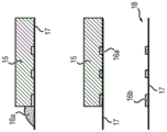
The method of forming the channels may be any method known to those skilled in the art used in the field of microfluidics or microfluidics, for example a method using NOA-81 as the dielectric material. As an example of a method of forming a via in a dielectric material, a method of using NOA-81 as a dielectric material is shown in fig. 6 and described in detail below.
The first step (fig. 6A) is a photolithography step. The patterned mask 14 is prepared with black portions corresponding to the surface to be imprinted and transparent portions corresponding to the surface not to be imprinted, the latter corresponding to the walls of the trenches to be imprinted. The mask is placed over a silicon wafer 12(Si wafer) covered with a thin SU-8 photoresist layer 13a before being irradiated with UV light. The SU-8 regions not covered by the mask (regions corresponding to the transparent portions of the mask) are crosslinked by UV light, while the SU-8 regions covered by the mask remain soluble and can be washed away after UV light treatment. This enables a micron or millimeter patterned thin layer 13b of cross-linked Su-8 to be obtained on a silicon wafer 12(Si wafer) after washing away the Su-8 that is not cross-linked by UV light. A first replica of these millimeter or micrometer patterns can then be achieved by PDMS (polydimethylsiloxane) (RTV) molding after the room temperature vulcanization step to obtain an imprinted pattern of grooves for the PDMS RTV 15 mold.
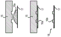
The second step (fig. 6B1 and 6B2) consists in making the NOA-81 bond (packer) 18 from the PDMS mold 15 with a pattern of micro-or millimetre structures (the same pattern as that obtained by SU-8). Two main techniques can be used to make the NOA-81 bond 18: stamping technique (fig. 6B1) or capillary action technique (fig. 6B2) [1 ]. For stamping techniques, the NOA-81 liquid 16a is first placed on a rigid substrate 17 (glass slide, Si wafer, etc.). The PDMS mold 15 was then placed over the NOA-81 liquid 16a, followed by a brief treatment with UV light through the PDMS mold 15 to partially insulate the NOA-81 liquid 16a (insulation) to enable a partially insulated NOA-81 liquid 16B to be obtained while leaving a thin layer of uncured polymer on the surface, thereby enabling the formation of the NOA-81 bond 18 (fig. 6B 1). For the capillary technique, the PDMS mold 15 is first brought into contact with a rigid substrate 17 (glass slide, Si wafer, etc.) before the NOA-81 liquid 16a is placed around the PDMS mold 15. Driven by capillary forces, the NOA-81 liquid 16a will be injected into the microstructure of the PDMS mold 15. To this end, a "porous" structure can be formed in the previous step by forming a mold of PDMS with various micro-pillars (small transparent dots are added on the mask to form these micro-pillars) in the regions not corresponding to the final channel region, so that the NOA-81 liquid can be driven by capillary forces between these micro-pillars. A short treatment with UV light was then carried out to obtain a partially insulated NOA-8116B and thus a NOA-81 bond 18 (figure 6B 2).
The third step consists in assembling the NOA-81 bond 18 (lower part) with the upper part (19+ optional 20b) so as to form the channel 8 (fig. 6C1, 6C2 and 6C 3). Two methods of assembly are contemplated. The NOA-81 bond 18 made by stamping or capillary techniques can be sealed under UV light through a rigid substrate 19 (e.g., a glass slide) (see fig. 6C2 and 6C3, respectively); alternatively, the NOA-81 bond 18 made by stamping or capillary techniques may also be sealed under UV light by another NOA-81 bond 21 comprising a rigid substrate 19 covered with a partially insulating NOA-81 layer 20b (see FIG. 6C1 in the case of the NOA-81 bond 18 made by stamping techniques; the case of the NOA-81 bond 18 made by capillary techniques is not shown). UV treatment of the partially insulated NOAs-8116 b, 20b enables complete insulation of the NOAs-81 and results in fully insulated NOAs-8116 c, 20c, enabling sealing of the lower section 23 with the upper section 24.
Two well-known types of electrode designs can be used to form the ground electrode and the high voltage electrode: metal deposition technology [2] or micron solid technology [3 ]. However, other methods for manufacturing the electrode are contemplated.
A method of forming an electrode by a metal deposition technique is shown in fig. 7A.
First, a substrate 25 (e.g., a glass slide) covered with a thin layer 26 of positive photoresist (e.g., S181) is provided (e.g., the substrate 25 may be prepared by spreading the positive photoresist uniformly over the substrate, especially by spin coating, followed by post-baking (hard cake) at about 115 ℃ for about 60S). The positive photoresist thin layer 26 on the substrate 25 is exposed to UV light at a desired wavelength through a patterned mask 27, the mask 27 including transparent portions (corresponding to the structure of the electrodes) and black portions, so that only regions of the photoresist thin layer 26 placed under the transparent portions of the mask 27 are exposed to the UV light. The photoresist is then developed so that the exposed areas dissolve in the developer and are washed away. Once the pattern of the mask is 'replicated' on the substrate 25 with the positive photoresist 26, a thin film of conductive material 28 (e.g., ITO-indium tin oxide) may be deposited on the substrate 25 and the positive photoresist 26 using various deposition methods (physical vapor deposition, sputtering methods, etc.). For example, the deposition of the ITO thin film may be performed via magnetron sputtering. To this end, the patterned photoresist is placed on a substrate holder in a magnetron sputtering chamber together with the substrate, and an ITO thin film is uniformly deposited on the substrate. After deposition of the conductive material 28, the photoresist layer 26 and the thin film of conductive material 28 thereon are removed, while the conductive material 28 deposited directly on the substrate 25 remains on the substrate 25, thereby forming the desired electrodes.
After thermal annealing, the substrate comprising the patterned thin film of conductor material can then be used as a substrate for making a support according to the invention comprising various channels that can be prepared as disclosed before using NOA-81 as a dielectric material as shown in fig. 6. In this case, the substrate including the patterned thin film of conductive material may be the substrate 17 or 19 of fig. 6. In these cases, electrodes made via deposition may be disposed above and below the main channel.
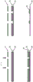
A method of forming an electrode by a micron solid technology (the method used in the examples of the present patent application) is shown in fig. 7B.
For this method, the ground electrode and the high voltage electrode embedded in the dielectric material of the support are formed in the following manner: a channel is first formed in the support (e.g. by the method described above, in particular the method shown in fig. 6), which is subsequently filled with the conductive material of the electrode. For this purpose, the channel is preferably formed using a pre-perforated upper side portion, so that the channel can be filled through a hole located in the upper side portion area above the channel.
To this end, a support 2 comprising, for example, a channel made according to fig. 6 (for example fig. 6C1) and a pre-perforated piece of PDMS (for example a block) 29a, 29b (for example with a hole having a diameter between 0.75mm and 1mm) is placed in a plasma cleaner (in particular for 30s to 2min) to carry out an oxygen plasma treatment. This oxygen plasma is able to activate the PDMS surface, so that the activated surface of the PDMS pre-punctures 29a, 29b can be bonded to the support 2 (for example, to the glass surface of the support). The holes of the PDMS pre-punched pieces 29a, 29c have to be connected to the holes of the upper side part of the support 2 in order to be able to fill the channels with the conductor material 30 and form the electrodes through these holes. The support 2 is then placed on a hot plate (for example at 200 ℃) and a wire of conductive material 30 with a low melting point is introduced into the channel through the holes of the PDMS pre-perforated block 29a and of the upper part of the support 2. Under heat, the conductive material 30 melts and fills the channel by capillary action. The wire is removed when molten conductor material 30 is present at the other end of the channel through the aperture of the second PDMS pre-perforated block 29 b. Upon cooling, the conductor material 30 hardens and forms an electrode. If necessary, a connection cable may be added to the hole of the PDMS pre-perforated block. By this method, electrodes are provided on both sides of the main channel, rather than above and below as with the deposition method.
Method for generating plasma
The microfluidic or millifluidic device according to the invention can be used to generate a plasma in a continuous manner in gas bubbles flowing through a main channel into a liquid.
The invention therefore also relates to a method for generating plasma in a continuous manner using a microfluidic or millifluidic device according to the invention, comprising the following steps:
(a) providing a liquid, circulating the liquid through a main microchannel or millimeter channel of a microfluidic or millimeter fluidic device,
(b) providing a gas, generating bubbles of said gas in said liquid, such that gas bubbles circulate with the liquid through a main micro-channel or milli-channel of a micro-fluidic or milli-fluidic device,
(c) a high voltage is applied between the high voltage electrode and the ground electrode to generate a plasma in the gas bubbles flowing through the primary microchannel or millimeter-channel of the microfluidic or millimeter-fluidic device.
The microfluidic or millifluidic device according to the invention is capable of forming a stream of gas bubbles in the liquid phase inside the main channel of the support, in particular under pressurized conditions. High voltage electrodes and ground electrodes located on opposite sides of and extending along the primary channel are capable of generating a high voltage electric field inside the primary channel. Due to the electric field generated inside the main channel, and more particularly due to the Dielectric Barrier Discharge (DBD), a plasma can thereby be generated in a continuous manner in the gas bubbles flowing in the main channel.
In the framework of the present invention, the plasma is generated "in a continuous manner" in the gas bubble, meaning that the bubble remains in the plasma state throughout its travel along the main microchannel or millimeter channel 3 between the ground electrode and the high voltage electrode.
Using a microfluidic or millifluidic device according to the invention enables:
-performing a hydrodynamic control, in particular of the size, the flow-through speed and the generation frequency of the bubbles, so as to have a reproducible homogeneous system, and
controlling the discharge and controlling the amount and frequency of energy injected into the bubbles, which allows to control the nature and concentration of the reactive species formed in the plasma.
The high voltage is typically between 1kV and 30kV, in particular between 5kV and 20kV, preferably between 10kV and 15 kV.
According to a first embodiment, the high voltage will be a variable voltage, more particularly a sinusoidal voltage, the frequency of which is advantageously between 1Hz and 10MHz, in particular between 100Hz and 1MHz, preferably between 100Hz and 10 kHz. This enables the generation of micro-discharges in the gas bubbles at a precise frequency. Advantageously, this frequency will be adapted to the experimental conditions, such as the nature of the gas, the flow rate of the bubbles, the kinetics of the target reaction, etc. In this case, the high voltage (peak-to-peak voltage) is typically between 1kV and 30kV, in particular between 5kV and 20kV, preferably between 10kV and 15 kV.
According to a second embodiment, the high voltage is a pulsed voltage. In this case, the applied voltage is high voltage only during a short pulse duration (typically 0.001 to 1 millisecond), the frequency of which is advantageously between 1Hz and 10MHz, in particular between 100Hz and 1MHz, preferably between 100Hz and 10 kHz. In this case, the high voltage (peak-to-peak voltage) is typically between 1kV and 30kV, in particular between 5kV and 20kV, preferably between 10kV and 15 kV.
As previously described, the high voltage is supplied by a high voltage power supply connected to the ground electrode 4 and the high voltage electrode 5.
The gas used in the method is any gas capable of generating plasma under high pressure conditions, such as air, argon, helium, nitrogen, oxygen, water vapor or mixtures thereof, and preferably air, argon, helium, nitrogen or mixtures thereof. The use of a gas phase confined in small gas bubbles enables the use of gases other than air and the control of the reactive species produced.
The width and height of the gas bubbles circulating in the main channel will depend on the width and height of the main channel. The width/height of the gas bubbles will typically be less than the width/height of the main channel, respectively. The length of each gas bubble will advantageously be between 1 μm and 10mm, in particular between 10 μm and 5mm, preferably between 100 μm and 3 mm. More particularly, the length of each gas bubble circulating in the main microchannel will advantageously be between 1 μm and 1000 μm, in particular between 10 μm and 500 μm, preferably between 100 μm and 300 μm, while the length of each gas bubble circulating in the main microchannel will advantageously be between 1mm and 10mm, in particular between 1mm and 5mm, preferably between 1mm and 3 mm. Advantageously, the gas bubbles have substantially the shape of spheres or flat spheres.
However, it is preferred to have smaller bubbles in order to increase the volume/surface area ratio of the bubbles, thereby maximizing the mass transfer efficiency between the gas and liquid phases.
These gas bubbles are able to flow with the liquid in the main channel, in particular by means of the pressure applied at the inlet of the support of the device. The pressure is advantageously between 1bar and 2bar (100 and 200 kPa).
The process according to the invention is advantageously carried out at room temperature, i.e. at a temperature comprised between 15 and 40 ℃, preferably between 20 and 30 ℃, in particular at a temperature of about 25 ℃. However, the method may be used at other temperatures, if necessary.
The plasma formed in the gas bubble is a partially ionized gas comprising molecules, atoms (typically in an excited state), ions, electrons, radicals, and the like. The plasma thus includes reactive species, e.g. ions (O)2 -、Ar+Etc.) or free radicals (OH °, O °, NO °, etc.). These reactive species can then react with each other to form new molecules that can be transported into the liquid, or conversely, the reactive species can be transported directly into the liquid to react with the reactants present in the liquid to form new molecules. The device according to the invention can therefore be used for chemical synthesis, more particularly for the synthesis of organic molecules.
The method according to the invention is shown in fig. 8, which shows the flow of gas bubbles in the liquid phase in a main channel surrounded by a high voltage electrode and a ground electrode in a point-to-face configuration. The dielectric barrier discharge generated between the two electrodes can generate plasma including the reactive speciesA body, the reaction substance exhibiting an electron (e)-) And a radical (. cndot.). These reactive species (or molecules formed in the gas bubbles by these reactive species) can then be transferred into the liquid as indicated by the arrows.
In the process according to the invention, gas bubbles (in which the reaction mass is generated) are adjacent to the liquid phase. Thus, in the method according to the invention, the loss of reactive species (which typically have a short half-life) during transfer from the gas bubble to the liquid is minimized, since the plasma (i.e. the reactive species) is generated continuously.
The liquid can include various components, such as one or several solvents and/or one or several reactants.
The solvent may be any solvent commonly used in organic chemistry, for example: water, aliphatic hydrocarbons (pentane, hexane, cyclopentane, cyclohexane), aromatic hydrocarbons (benzene, toluene), alcohols (methanol, ethanol, n-propanol, isopropanol, n-butanol, isobutanol, tert-butanol), ethers (1, 4-dioxane, diethyl ether, Tetrahydrofuran (THF)), esters (ethyl acetate), ketones (acetone), halogenated solvents (chloroform, dichloromethane, dichloroethane), dimethyl sulfoxide (DMSO), acetonitrile, Dimethylformamide (DMF) or mixtures thereof. Specifically, it may be water, alcohol (e.g., methanol, ethanol, n-propanol, isopropanol, n-butanol, isobutanol, t-butanol), or a mixture thereof.
The reactant can be any reactant that can be used in organic chemistry, such as a monomer. It may be, in particular, Methyl Methacrylate (MMA), phenol, etc. If the reactants are in liquid form at the operating temperature, they can be used separately without any solvent.
Examples of the invention
Example 1
Materials and methods
The thiol-ene based resin NOA-81(Norland Optical additive) was used primarily to prepare microfluidic or millifluidic devices according to the present invention. This resin was chosen instead of the traditionally used PDMS (polydimethylsiloxane) because of its good physical, chemical, electrical and optical properties: i) unlike PDMS devices, NOA-81 microreactors are impermeable to gases such as air and water vapor, which ensures a closed environment [1] to the plasma; ii) the cured NOA-81 has a high modulus of elasticity (typically 1GPa), which avoids the sagging (bagging) effect [1 ]; iii) NOA-81 exhibits less solvent swelling (swelling) effect than PDMS [1 ]; iv) the NOA-81 has a dielectric constant of 4.05 at 1MHz and also behaves as an insulating material; v) NOA-81 has high transmittance in the visible and near UV range, enabling in situ (in situ) discharge diagnostics (optical emission spectroscopy (OES) or ultra fast camera measurements). Thanks to these properties, NOA-81 is a good candidate for the fabrication of plasma micro-or millimeter reactors.
The struts were prepared as shown in fig. 6A, 6B1, and 6C1 and described in detail in the specification. The geometry of the supports used is shown in fig. 9, with small circles showing the tiny pillars used to form the PDMC mold. Which corresponds to a support with a flow concentrating design for generating gas bubbles. The dimensions of the channels used in this experiment were as follows: wg=240μm,Wl=240μm,Wo=120μm,Wout=240μm,Wd=120μm,We=240μm。
The ground electrode and the high voltage electrode were made of an alloy of 52% In and 48% In (Indium Corporation of America) In a face-to-face configuration according to the method shown In fig. 7B and described In detail In the specification.
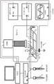
Fig. 9 shows the complete apparatus for observing the plasma discharge. The two electrodes of the microreactor are connected to a high voltage power supply and ground, respectively. The sine wave generated by the function generator is amplified to tens of thousands of volts by a signal amplifier (Trek, 20/20C). The stable generation of bubbles in the flow concentration geometry was enabled by a computer controlled pressure controller (Fluigent, MCFS-EZ system, france). A current probe is disposed between the microreactor and a ground connection to electrically detect plasma discharge. An iCCD camera (Pimax4, Princeton Instruments) was triggered by a function generator to collect images of the plasma discharge through a microscope (Leica Z16 APO). In order to detect weak luminescence at the time of discharge, a dark environment is indispensable.
The liquid selected was deionized water and the working gas was argon. The driving pressures for the liquid and gas phases were 88mbar and 86mbar (8.8 and 8.6kPa), respectively.
The high voltage was gradually increased until a discharge was observed. In this example, the Pk-Pk voltage is 12.51kV and the frequency is 228 Hz.
Results
Fig. 10 shows the main result of the plasma discharge obtained by means of two electrodes in a bubble passing in the main channel. During the experiment, the plasma bubbles were observed to move through the light emitting section of the microchannel.
Example 2
Materials and methods:
in order to meter the radical species transferred from the plasma bubble to the liquid phase, an EPR (electron paramagnetic resonance) experiment was performed. For these experiments, argon bubbles were fixed in cavities arranged along the main channel (where the liquid flows). With this geometry, the liquid residence time can be more easily controlled. The experiment was performed at a liquid flow of 10. mu.L/min. Under these conditions, the time of exposure to the plasma was 0.9S, corresponding to a surface to liquid volume ratio S/V of 2000m for exposure to the plasma phase2/m3。
The liquid phase was deionized water including 0.4mol/L of 5, 5-dimethyl-pyrroline-N-oxide (DMPO), which is a commonly used spin-trap.
The high voltage was gradually increased until a discharge was observed. In this example, the Pk-Pk voltage is 3kV and the frequency is 2 kHz.
The liquid phase with spin traps passes through the main channel and traps the radicals initially generated in the plasma bubbles, which are fixed in the cavity. The reacted solution was then collected at the outlet of the reactor and after 30 minutes at the end of the experiment the product mixture was passed through an EPR spectrometer. A reference experiment was performed in which the same DMPO solution was passed through a reactor without plasma discharge.
As a result:
figure 11 shows the EPR spectrum of the collected liquid. It showed the presence of. DMPO-OH and. DMPO-H, while no significant signal was detected in the reference sample.
To further confirm the presence of these two free radicals, spectral simulations were performed by public EPR software (Winsim v.1.0, 2002). Winsim is a specialized program used to compute simulations of isotropic radicals for multiple free rotations in complex systems. Software and databases are provided by the National Institute of Environmental Health Sciences (NIEHS) in the United states. The simulation parameters are shown in table 1.
Table 1: parameters for EPR spectral modeling
Fig. 12 compares the simulated signal with the EPR spectrum obtained by the experimental results. The high similarity between the simulated and measured spectra confirms that DMPO-OH and DMPO-H are detected in the liquid phase. The concentration ratio of. DMPO-OH and. DMPO-H can also be calculated by comparing the areas of the two substances based on the simulation (Table 1), which is about 0.8.
Reference to the literature
[1]D.Bartolo,G.Degré,P.Nghe,V.Studer,"Microfluidic stickers",Lab.Chip,vol.8,no 2,p.274-279,janv.2008。
[2]G.Schelcher,C.Guyon,S.Ognier,S.Cavadias,E.Martinez,V.Taniga,L.Malaquin,P.Tabeling,M.Tatoulian,"Cyclic olefin copolymer plasma millireactors",Lab.Chip,vol.14,no 16,p.3037-3042,
2014。
[3]A.C.Siegel,S.S.Shevkoplyas,D.B.Weibel,D.A.Bruzewicz,A.W.Martinez,et G.M.Whitesides,"Cofabrication of Electromagnets and Microfluidic Systems in Poly(dimethylsiloxane)",Angew.Chem.,vol.118,no 41,p.7031-7036,oct.2006。
[4]P.Garstecki,I.Gitlin,W.DiLuzio,G.M.Whitesides,E.Kumacheva,H.A.Stone,"Formation of monodisperse bubbles in a microfluidic flow-focusing device",Appl.Phys.Lett.,vol.85,no 13,p.2649-2651,sept.2004。
[5]M.A.Malik,"Water Purification by Plasmas:Which Reactors are Most Energy Efficient?",Plasma Chem Plasma Process,vol.30,no 1,p.21 31,nov.2009。
[6]T.Yano,I.Uchiyama,F.Fukawa,K.Teranishi,and N.Shimomura,"Water Treatment by Atmospheric Discharge Produced with Nanosecond Pulsed Power",in IEEE International Power Modulators and High Voltage Conference,Proceedings of the 2008,2008,pp.80–83。
[7]Y.Matsui,N.Takeuchi,K.Sasaki,R.Hayashi,K.Yasuoka,"Experimental and theoretical study of acetic-acid decomposition by a pulsed dielectric-barrier plasma in a gas–liquid two-phase flow",Plasma Sources Sci.Technol.20(2011)034015(11pp)。
[8]Y.Yamanishi,S.Sameshima,H.Kuriki,S.Sakuma,F.Arai,"Transportation of mono-dispersed micro-plasma bubble in microfluidic chip under atmospheric pressure",Transducers 2013,Barcelona,SPAIN,16-20 June 2013。
[9]US 2006/0034736。
[10]US 2008/0108122。
[11]GB 2 466 664 A。