CN108808237B - Planar omnidirectional circularly polarized antenna - Google Patents
Planar omnidirectional circularly polarized antenna Download PDFInfo
- Publication number
- CN108808237B CN108808237B CN201810691912.6A CN201810691912A CN108808237B CN 108808237 B CN108808237 B CN 108808237B CN 201810691912 A CN201810691912 A CN 201810691912A CN 108808237 B CN108808237 B CN 108808237B
- Authority
- CN
- China
- Prior art keywords
- metal layer
- substrate
- center
- front metal
- circularly polarized
- Prior art date
- Legal status (The legal status is an assumption and is not a legal conclusion. Google has not performed a legal analysis and makes no representation as to the accuracy of the status listed.)
- Active
Links
Images


Classifications
-
- H—ELECTRICITY
- H01—ELECTRIC ELEMENTS
- H01Q—ANTENNAS, i.e. RADIO AERIALS
- H01Q1/00—Details of, or arrangements associated with, antennas
- H01Q1/50—Structural association of antennas with earthing switches, lead-in devices or lightning protectors
-
- H—ELECTRICITY
- H01—ELECTRIC ELEMENTS
- H01Q—ANTENNAS, i.e. RADIO AERIALS
- H01Q1/00—Details of, or arrangements associated with, antennas
- H01Q1/36—Structural form of radiating elements, e.g. cone, spiral, umbrella; Particular materials used therewith
- H01Q1/38—Structural form of radiating elements, e.g. cone, spiral, umbrella; Particular materials used therewith formed by a conductive layer on an insulating support
Landscapes
- Variable-Direction Aerials And Aerial Arrays (AREA)
Abstract
Description
技术领域technical field
本发明属于天线装备技术领域,更具体地说,是涉及一种平面全向圆极化天线。The invention belongs to the technical field of antenna equipment, and more particularly, relates to a plane omnidirectional circularly polarized antenna.
背景技术Background technique
天线技术是无线通信与探测技术中不可或缺的重要一环,天线为无线射频通信提供了信息交换通道。传统的天线主要采用线极化方式进行设计,而线极化又分为水平极化和垂直极化,在天线的使用过程中,接收天线和发射天线必须处于同一线极化方式才可以正常工作,因此,天线对于安装方式极其敏感,不利于在复杂多变环境中的应用,并且传统天线的波束宽度不会很宽,限制了单个天线的通信角度范围,若需要宽角度通信,就需要多个天线同时工作,在增加系统的重量和成本的同时也增加了系统的复杂度,对于整个系统的设计是极为不利的。同时,在使用传统天线的过程中,为了保证性能,往往需要单独加工天线,然后将天线与系统通过预留的馈电接口进行连接,不能与通信系统实现一体化集成,增加了工艺的复杂度,降低了生产效率。Antenna technology is an indispensable part of wireless communication and detection technology, and antenna provides information exchange channel for wireless radio frequency communication. The traditional antenna is mainly designed with linear polarization, and the linear polarization is divided into horizontal polarization and vertical polarization. During the use of the antenna, the receiving antenna and the transmitting antenna must be in the same linear polarization to work normally. , Therefore, the antenna is extremely sensitive to the installation method, which is not conducive to the application in complex and changeable environments, and the beam width of the traditional antenna is not very wide, which limits the communication angle range of a single antenna. The simultaneous operation of multiple antennas increases the weight and cost of the system and also increases the complexity of the system, which is extremely unfavorable for the design of the entire system. At the same time, in the process of using the traditional antenna, in order to ensure the performance, it is often necessary to process the antenna separately, and then connect the antenna to the system through the reserved feeder interface, which cannot be integrated with the communication system, which increases the complexity of the process. , reducing production efficiency.
发明内容SUMMARY OF THE INVENTION
本发明的目的在于提供一种平面全向圆极化天线,以解决现有技术中存在的单个天线波束宽度窄、覆盖范围小且不能与通信系统实现一体化集成的技术问题。The purpose of the present invention is to provide a plane omnidirectional circularly polarized antenna to solve the technical problems in the prior art that a single antenna has a narrow beam width, a small coverage and cannot be integrated with a communication system.
为实现上述目的,本发明采用的技术方案是:提供一种平面全向圆极化天线,包括:基板、设于所述基板前侧的前金属层、围绕所述基板中心设于所述前金属层外周的多个前金属辐射结构、设于所述基板后侧的后金属层、围绕所述基板中心设于所述后金属层外周的多个后金属辐射结构、设于所述基板中心处的金属化馈电孔、围绕所述金属化馈电孔分布且贯通所述前金属层和所述后金属层的多个金属化屏蔽通孔组及设于所述前金属层前侧且与所述金属化馈电孔通过第一键合金属丝连接的射频芯片结构;所述前金属辐射结构的内端与所述前金属层的外缘连接,所述后金属辐射结构的内端与所述后金属层的外缘连接;所述前金属层的中心与所述后金属层的中心分别与所述基板的中心重合。In order to achieve the above object, the technical solution adopted in the present invention is to provide a plane omnidirectional circularly polarized antenna, comprising: a substrate, a front metal layer arranged on the front side of the substrate, and a front metal layer arranged around the center of the substrate on the front side of the substrate. a plurality of front metal radiating structures on the periphery of the metal layer, a rear metal layer disposed on the back side of the substrate, a plurality of rear metal radiating structures disposed on the periphery of the rear metal layer around the center of the substrate, and disposed in the center of the substrate a metallization feed hole at the position, a plurality of metallization shielding through hole groups distributed around the metallization feed hole and passing through the front metal layer and the rear metal layer, and a plurality of metallization shielding via groups disposed on the front side of the front metal layer and an RF chip structure connected to the metallized feed hole through a first bonding wire; the inner end of the front metal radiation structure is connected to the outer edge of the front metal layer, and the inner end of the rear metal radiation structure connected with the outer edge of the rear metal layer; the center of the front metal layer and the center of the rear metal layer respectively coincide with the center of the substrate.
进一步地,所述基板为圆形基板,所述前金属层和所述后金属层均为圆形金属层。Further, the substrate is a circular substrate, and both the front metal layer and the rear metal layer are circular metal layers.
进一步地,所述金属化屏蔽通孔组具有至少八个,每个所述金属化屏蔽通孔组分别包括多个沿所述基板径向分布的金属化屏蔽通孔。Further, there are at least eight metallized shielding through-hole groups, and each metallized shielding through-hole group respectively includes a plurality of metallized shielding through-holes distributed along the radial direction of the substrate.
进一步地,所述金属化屏蔽通孔组具有至少八个,每个所述金属化屏蔽通孔组分别包括一个金属化屏蔽通孔。Further, there are at least eight metallized shielding through hole groups, and each metallization shielding through hole group includes one metallization shielding through hole respectively.
进一步地,所述前金属辐射结构包括围绕所述前金属层均匀分布且长轴分别平行于所述前金属层径向的多个前金属径向条及设于所述前金属径向条外端且沿所述前金属层切向分布的前金属切向条;所述后金属辐射结构包括围绕所述后金属层均匀分布且长轴分别平行于所述后金属层径向的多个后金属径向条及设于所述后金属径向条外端且沿所述后金属层切向分布的前金属切向条;相邻的所述前金属切向条之间间隔设置,相邻的所述后金属切向条之间间隔设置。Further, the front metal radiating structure includes a plurality of front metal radial strips which are evenly distributed around the front metal layer and whose long axes are respectively parallel to the radial direction of the front metal layer, and are disposed outside the front metal radial strips. front metal tangential strips at the ends and tangentially distributed along the front metal layer; the rear metal radiating structure includes a plurality of rear metal radiating structures evenly distributed around the rear metal layer and whose major axes are respectively parallel to the radial direction of the rear metal layer Metal radial strips and front metal tangential strips disposed at the outer ends of the rear metal radial strips and tangentially distributed along the rear metal layer; adjacent front metal tangential strips are arranged at intervals, adjacent to each other. The rear metal tangential strips are spaced apart.
进一步地,所述前金属切向条和所述后金属切向条在所述基板前板面上的投影相互重合,所述前金属径向条和所述后金属径向条在所述基板前板面上的投影围绕所述基板的中心交替设置。Further, the projections of the front metal tangential strips and the rear metal tangential strips on the front plate surface of the substrate coincide with each other, and the front metal radial strips and the rear metal radial strips are on the base plate. The projections on the front panel are alternately arranged around the center of the substrate.
进一步地,所述前金属层上设有中心与所述前金属层中心重合的前辐射缝隙环组,所述后金属层上设有中心与所述后金属层中心重合的后辐射缝隙环组。Further, the front metal layer is provided with a front radiating slot ring group whose center coincides with the center of the front metal layer, and the rear metal layer is provided with a rear radiating gap ring group whose center coincides with the center of the rear metal layer. .
进一步地,所述前辐射缝隙环组包括多个内径逐渐增加且中心分别与所述前金属层中心重合的前辐射缝隙环,所述后辐射缝隙环组包括多个内径逐渐增加且中心分别与所述后金属层中心重合的后辐射缝隙环;或者,所述前辐射缝隙环组包括一个中心与所述前金属层中心重合的前辐射缝隙环,所述后辐射缝隙环组包括一个中心与所述后金属层中心重合的后辐射缝隙环。Further, the front radiating slot ring group includes a plurality of front radiating slot rings whose inner diameters gradually increase and whose centers respectively coincide with the centers of the front metal layers, and the rear radiating slot ring groups include a plurality of which inner diameters increase gradually and whose centers are respectively the same as the center of the front metal layer. The rear radiating slot ring with the center of the rear metal layer coincident; or, the front radiating slot ring group includes a front radiating slot ring whose center is coincident with the center of the front metal layer, and the rear radiating slot ring group includes a center and The rear radiating slot ring with the center of the rear metal layer overlapping.
进一步地,所述射频芯片结构包括设于所述前金属层前侧的射频芯片、罩设于所述射频芯片前侧的前罩体、设于所述前罩体边缘的信号传输通孔及设于所述信号传输通孔前端外周的焊盘组件;所述射频芯片通过信号传输线与所述信号传输通孔连接,所述射频芯片通过所述第一键合金属丝与所述金属化馈电孔连接。Further, the radio frequency chip structure includes a radio frequency chip disposed on the front side of the front metal layer, a front cover body disposed on the front side of the radio frequency chip, a signal transmission through hole disposed on the edge of the front cover body, and A pad assembly arranged on the outer periphery of the front end of the signal transmission through hole; the radio frequency chip is connected to the signal transmission through hole through a signal transmission line, and the radio frequency chip is connected to the metallization feed through the first bonding wire electrical connection.
进一步地,所述信号传输线和所述前金属层之间以及所述信号传输通孔的底端和所述前金属层之间还设有隔离垫层,所述信号传输线通过第二键合金属丝与所述射频芯片连接。Further, an isolation pad layer is also provided between the signal transmission line and the front metal layer and between the bottom end of the signal transmission through hole and the front metal layer, and the signal transmission line passes through the second bonding metal. The wire is connected with the radio frequency chip.
本发明提供的平面全向圆极化天线的有益效果在于:与现有技术相比,本发明平面全向圆极化天线,金属化屏蔽通孔组组成了径向功分结构,将馈入的信号分为与金属化屏蔽通孔组数量一致的多个,然后采用类波导形式,将能量传输出去,实现水平面内360°均匀辐射,而在垂直面内有一定波束宽度,对方向性不敏感,既可以接收水平面上各个方向的信号,发射的信号也可以被水平面上任意方位的接收端接收;前金属辐射结构和后金属辐射结构用于调节加载的前金属辐射结构和后金属辐射结构产生的电场与类波导结构(前金属层和后金属层)产生的电场的方向的夹角,以控制两个电场的相位差,进而实现圆极化特性,在安装方式上,只要将发射天线和接收天线对准,即可实现稳定有效的即时通信,降低了系统的安装与调试难度;射频芯片结构用于实现多层有功能的介质基板间互连以及与外部接口之间的信号互通,通过这种三维堆叠技术,实现天线本体、射频芯片结构以及外部系统之间的互连。本发明提供的平面全向圆极化天线波束宽度宽、覆盖范围大,可实现任意角度、任意放置方式的通信方案,可以有效降低系统中天线的数量,降低系统的调试难度,提高系统的运行效率,还可方便的实现天线与系统的一体化集成。The beneficial effect of the planar omnidirectional circularly polarized antenna provided by the present invention is: compared with the prior art, the planar omnidirectional circularly polarized antenna of the present invention has a radial power division structure formed by the metallized shielding through-hole group, which feeds the The signal is divided into a number of the same number of metallized shielding through-hole groups, and then the waveguide-like form is used to transmit the energy to achieve 360° uniform radiation in the horizontal plane, and there is a certain beam width in the vertical plane, which has no effect on directivity. Sensitive, it can receive signals from all directions on the horizontal plane, and the transmitted signal can also be received by the receiving end in any direction on the horizontal plane; the front metal radiation structure and the rear metal radiation structure are used to adjust the loading front metal radiation structure and rear metal radiation structure The angle between the generated electric field and the direction of the electric field generated by the waveguide-like structure (front metal layer and rear metal layer) is used to control the phase difference between the two electric fields, thereby realizing circular polarization characteristics. By aligning with the receiving antenna, stable and effective instant communication can be achieved, which reduces the difficulty of system installation and debugging; the RF chip structure is used to achieve interconnection between multi-layer functional dielectric substrates and signal intercommunication with external interfaces. Through this three-dimensional stacking technology, the interconnection between the antenna body, the radio frequency chip structure and the external system is realized. The plane omnidirectional circularly polarized antenna provided by the invention has a wide beam width and a large coverage, can realize a communication scheme of any angle and any placement method, can effectively reduce the number of antennas in the system, reduce the debugging difficulty of the system, and improve the operation of the system Efficiency, and it is also convenient to realize the integrated integration of the antenna and the system.
附图说明Description of drawings
为了更清楚地说明本发明实施例中的技术方案,下面将对实施例或现有技术描述中所需要使用的附图作简单地介绍,显而易见地,下面描述中的附图仅仅是本发明的一些实施例,对于本领域普通技术人员来讲,在不付出创造性劳动性的前提下,还可以根据这些附图获得其他的附图。In order to illustrate the technical solutions in the embodiments of the present invention more clearly, the following briefly introduces the accompanying drawings that need to be used in the description of the embodiments or the prior art. Obviously, the drawings in the following description are only for the present invention. In some embodiments, for those of ordinary skill in the art, other drawings can also be obtained according to these drawings without any creative effort.
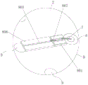
图1为本发明实施例提供的平面全向圆极化天线的立体结构示意图一;1 is a schematic diagram 1 of a three-dimensional structure of a planar omnidirectional circularly polarized antenna provided by an embodiment of the present invention;
图2为本发明实施例提供的平面全向圆极化天线的立体结构示意图二;FIG. 2 is a schematic diagram 2 of a three-dimensional structure of a planar omnidirectional circularly polarized antenna provided by an embodiment of the present invention;
图3为本发明实施例提供的平面全向圆极化天线的主视结构示意图;3 is a schematic structural diagram of a front view of a planar omnidirectional circularly polarized antenna provided by an embodiment of the present invention;
图4为图3的A-A剖视图;Fig. 4 is the A-A sectional view of Fig. 3;
图5为图4的局部放大图;Fig. 5 is a partial enlarged view of Fig. 4;
图6为本发明实施例提供的平面全向圆极化天线的未装配前罩体的立体结构示意图;6 is a schematic three-dimensional structural diagram of an unassembled front cover of a planar omnidirectional circularly polarized antenna provided by an embodiment of the present invention;
图7为图8的B部放大图;FIG. 7 is an enlarged view of part B of FIG. 8;
图8为本发明实施例提供的平面全向圆极化天线的仿真反射系数图;8 is a simulated reflection coefficient diagram of a planar omnidirectional circularly polarized antenna provided by an embodiment of the present invention;
图9为本发明实施例提供的平面全向圆极化天线的辐射3D方向图;9 is a radiation 3D pattern of a planar omnidirectional circularly polarized antenna provided by an embodiment of the present invention;
图10为本发明实施例提供的平面全向圆极化天线的轴比图。FIG. 10 is an axial ratio diagram of a planar omnidirectional circularly polarized antenna provided by an embodiment of the present invention.
其中,图中各附图标记:Among them, each reference sign in the figure:
1-基板;2-前金属层;3-前金属辐射结构;301-前金属径向条;302-前金属切向条;4-后金属层;5-后金属辐射结构;501-后金属径向条;502-后金属切向条;6-金属化馈电孔;7-第一键合金属丝;8-射频芯片结构;801-射频芯片;802-前罩体;803-信号传输通孔;805-信号传输线;806-隔离垫层;807-第二键合金属丝;9-金属化屏蔽通孔;10-前辐射缝隙环;11-后辐射缝隙环1-substrate; 2-front metal layer; 3-front metal radiation structure; 301-front metal radial strip; 302-front metal tangential strip; 4-back metal layer; 5-back metal radiation structure; 501-back metal Radial strip; 502-Rear metal tangential strip; 6-Metalized feed hole; 7-First bonding wire; 8-RF chip structure; 801-RF chip; 802-Front cover body; 803-Signal transmission 805-signal transmission line; 806-isolation pad; 807-second bonding wire; 9-metallized shielding through hole; 10-front radiation slot ring; 11-back radiation slot ring
具体实施方式Detailed ways
为了使本发明所要解决的技术问题、技术方案及有益效果更加清楚明白,以下结合附图及实施例,对本发明进行进一步详细说明。应当理解,此处所描述的具体实施例仅仅用以解释本发明,并不用于限定本发明。In order to make the technical problems, technical solutions and beneficial effects to be solved by the present invention clearer, the present invention will be further described in detail below with reference to the accompanying drawings and embodiments. It should be understood that the specific embodiments described herein are only used to explain the present invention, but not to limit the present invention.
需要说明的是,当元件被称为“固定于”或“设置于”另一个元件,它可以直接在另一个元件上或者间接在该另一个元件上。当一个元件被称为是“连接于”另一个元件,它可以是直接连接到另一个元件或间接连接至该另一个元件上。It should be noted that when an element is referred to as being "fixed to" or "disposed on" another element, it can be directly on the other element or indirectly on the other element. When an element is referred to as being "connected to" another element, it can be directly connected to the other element or indirectly connected to the other element.
需要理解的是,术语“长度”、“宽度”、“上”、“下”、“前”、“后”、“左”、“右”、“竖直”、“水平”、“顶”、“底”“内”、“外”等指示的方位或位置关系为基于附图所示的方位或位置关系,仅是为了便于描述本发明和简化描述,而不是指示或暗示所指的装置或元件必须具有特定的方位、以特定的方位构造和操作,因此不能理解为对本发明的限制。It is to be understood that the terms "length", "width", "upper", "lower", "front", "rear", "left", "right", "vertical", "horizontal", "top" , "bottom", "inside", "outside", etc. indicate the orientation or positional relationship based on the orientation or positional relationship shown in the accompanying drawings, which are only for the convenience of describing the present invention and simplifying the description, rather than indicating or implying the indicated device. Or elements must have a particular orientation, be constructed and operate in a particular orientation, and therefore should not be construed as limiting the invention.
此外,术语“第一”、“第二”仅用于描述目的,而不能理解为指示或暗示相对重要性或者隐含指明所指示的技术特征的数量。由此,限定有“第一”、“第二”的特征可以明示或者隐含地包括一个或者更多个该特征。在本发明的描述中,“多个”的含义是两个或两个以上,除非另有明确具体的限定。In addition, the terms "first" and "second" are only used for descriptive purposes, and should not be construed as indicating or implying relative importance or implying the number of indicated technical features. Thus, a feature defined as "first" or "second" may expressly or implicitly include one or more of that feature. In the description of the present invention, "plurality" means two or more, unless otherwise expressly and specifically defined.
请一并参阅图1至图6,现对本发明提供的平面全向圆极化天线进行说明。所述平面全向圆极化天线,包括基板1、设于基板1前侧的前金属层2、围绕基板1中心设于前金属层2外周的多个前金属辐射结构3、设于基板1后侧的后金属层4、围绕基板1中心设于后金属层4外周的多个后金属辐射结构5、设于基板1中心处的金属化馈电孔6、围绕金属化馈电孔6分布且贯通前金属层2和后金属层4的多个金属化屏蔽通孔组及设于前金属层2前侧且与金属化馈电孔6通过第一键合金属丝7连接的射频芯片结构8;前金属辐射结构3的内端与前金属层2的外缘连接,后金属辐射结构5的内端与后金属层4的外缘连接;前金属层2的中心与后金属层4的中心分别与基板1的中心重合。Please refer to FIG. 1 to FIG. 6 together, and now the planar omnidirectional circularly polarized antenna provided by the present invention will be described. The planar omnidirectional circularly polarized antenna includes a
本发明提供的平面全向圆极化天线,与现有技术相比,金属化屏蔽通孔组组成了径向功分结构,将馈入的信号分为与金属化屏蔽通孔组数量一致的多个,然后采用类波导形式,将能量传输出去,实现水平面内360°均匀辐射,而在垂直面内有一定波束宽度,对方向性不敏感,既可以接收水平面上各个方向的信号,发射的信号也可以被水平面上任意方位的接收端接收;前金属辐射结构和后金属辐射结构用于调节加载的前金属辐射结构3和后金属辐射结构5产生的电场与类波导结构(前金属层2和后金属层4)产生的电场的方向的夹角,以控制两个电场的相位差,进而实现圆极化特性,在安装方式上,只要将发射天线和接收天线对准,即可实现稳定有效的即时通信,降低了系统的安装与调试难度,且与现有的工艺相兼容;射频芯片结构8用于实现多层有功能的介质基板间互连以及与外部接口之间的信号互通,通过这种三维堆叠技术,实现天线本体、射频芯片结构8以及外部系统之间的互连。本发明提供的平面全向圆极化天线波束宽度宽、覆盖范围大,可实现任意角度、任意放置方式的通信方案,可以有效降低系统中天线的数量,降低系统的调试难度,提高系统的运行效率,还可方便的实现天线与系统的一体化集成。Compared with the prior art, in the planar omnidirectional circularly polarized antenna provided by the present invention, the group of metallized shielding through holes forms a radial power division structure, and the fed signal is divided into the same number as the number of groups of metallized shielding through holes. Multiple, and then adopt the form of a waveguide to transmit the energy to achieve 360° uniform radiation in the horizontal plane, while in the vertical plane, there is a certain beam width, which is not sensitive to directionality. It can receive signals in all directions on the horizontal plane, and transmit The signal can also be received by the receiving end at any orientation on the horizontal plane; the front metal radiation structure and the rear metal radiation structure are used to adjust the electric field generated by the loaded front
具体地,作为本发明提供的平面全向圆极化天线的一种具体实施方式,前金属层2和后金属层4为镀金层。Specifically, as a specific embodiment of the planar omnidirectional circularly polarized antenna provided by the present invention, the
进一步地,请一并参阅图1至图6,作为本发明提供的平面全向圆极化天线的一种具体实施方式,为了方便制造,同时充分实现水平面360°波束的均匀覆盖,并更好的实现圆极化特性,基板1为圆形基板,前金属层2和后金属层4均为圆形金属层。Further, please refer to FIG. 1 to FIG. 6 together, as a specific embodiment of the planar omnidirectional circularly polarized antenna provided by the present invention, in order to facilitate the manufacture, at the same time fully realize the uniform coverage of the horizontal plane 360° beam, and better To achieve circular polarization characteristics, the
进一步地,作为本发明提供的平面全向圆极化天线的一种具体实施方式,金属化屏蔽通孔组具有至少八个,每个金属化屏蔽通孔组分别包括多个沿基板1径向分布的金属化屏蔽通孔9。金属化屏蔽通孔组配合构成径向功分结构,将馈入的信号一分八,然后采用类波导形式将能量传输出去,实现水平面内360°均匀辐射。Further, as a specific embodiment of the planar omnidirectional circularly polarized antenna provided by the present invention, the metallized shielding through hole group has at least eight, Distributed metallization shields vias 9 . The metallized shielding through-hole group cooperates to form a radial power division structure, which divides the incoming signal into eight parts, and then transmits the energy in a waveguide-like form to achieve 360° uniform radiation in the horizontal plane.
进一步地,参阅图1至图7,作为本发明提供的平面全向圆极化天线的一种具体实施方式,金属化屏蔽通孔组具有至少八个,为了最大化的降低径向功分结构的结构复杂程度,每个金属化屏蔽通孔组分别包括一个金属化屏蔽通孔9。Further, referring to FIG. 1 to FIG. 7 , as a specific embodiment of the planar omnidirectional circularly polarized antenna provided by the present invention, the metallized shielding through hole group has at least eight, in order to maximize the reduction of the radial power division structure According to the structural complexity, each metallized shielding through hole group includes one metallized shielding through
进一步地,请参阅图1至图3及图6,作为本发明提供的平面全向圆极化天线的一种具体实施方式,前金属辐射结构3包括围绕前金属层2均匀分布且长轴分别平行于前金属层2径向的多个前金属径向条301及设于前金属径向条301外端且沿前金属层2切向分布的前金属切向条302;后金属辐射结构5包括围绕后金属层4均匀分布且长轴分别平行于后金属层4径向的多个后金属径向条501及设于后金属径向条501外端且沿后金属层4切向分布的后金属切向条502;相邻的前金属切向条302之间间隔设置,相邻的后金属切向条502之间间隔设置。前金属径向条301的内端和前金属层2外缘连接;后金属径向条501的内端和后金属层4外缘连接。前金属切向条302为弧形结构,后金属切向条502为弧形结构。Further, please refer to FIG. 1 to FIG. 3 and FIG. 6 , as a specific embodiment of the planar omnidirectional circularly polarized antenna provided by the present invention, the front
需要注意的是,前金属径向条301和前金属切向条302配合构成“L”型的金属结构,该“L”型的金属结构均朝向一个旋向偏斜;后金属径向条501和后金属切向条502配合构成“L”型的金属结构,该“L”型的金属结构均朝向另一个旋向偏斜。前金属辐射结构3和后金属辐射结构5使加载的金属辐射结构产生的电场与类波导结构产生的电场方向相互垂直,且通过调节前金属辐射结构3和后金属辐射结构5,使得两个电场的相位差正好为90°,以更好的实现圆极化特性。It should be noted that the front metal radial strips 301 and the front metal
进一步地,作为本发明提供的平面全向圆极化天线的一种具体实施方式,前金属切向条302和后金属切向条502在基板1前板面上的投影相互重合,前金属径向条301和后金属径向条501在基板1前板面上的投影围绕基板1的中心交替设置,进而有效实现使加载的金属辐射结构产生的电场与类波导结构产生的电场方向相互垂直的技术效果。Further, as a specific embodiment of the planar omnidirectional circularly polarized antenna provided by the present invention, the projections of the front metal
进一步地,参阅图1至图3及图6,作为本发明提供的平面全向圆极化天线的一种具体实施方式,前金属层2上设有中心与前金属层2中心重合的前辐射缝隙环组,后金属层4上设有中心与后金属层4中心重合的后辐射缝隙环组。前辐射缝隙环组与后辐射缝隙环组在前后方向上的位置一一对应,在前金属层2和后金属层4(类波导结构)上开有规律的辐射缝隙,可以通过调节辐射缝隙的大小以及间距,调整在法线方向上的辐射能量,最终减小天线法线方向的辐射能量。Further, referring to FIG. 1 to FIG. 3 and FIG. 6, as a specific embodiment of the planar omnidirectional circularly polarized antenna provided by the present invention, the
进一步地,请参阅图1至图3及图6,作为本发明提供的平面全向圆极化天线的一种具体实施方式,为了合理减小天线法线方向的辐射能量,前辐射缝隙环组包括多个内径逐渐增加且中心分别与前金属层2中心重合的前辐射缝隙环10,后辐射缝隙环组包括多个内径逐渐增加且中心分别与后金属层4中心重合的后辐射缝隙环11。其中,相邻的前辐射缝隙环10间距一致,相邻的后辐射缝隙环11间距一致;前辐射缝隙环10与后辐射缝隙环11在前后方向上一一对应。Further, please refer to FIG. 1 to FIG. 3 and FIG. 6, as a specific embodiment of the planar omnidirectional circularly polarized antenna provided by the present invention, in order to reasonably reduce the radiation energy in the normal direction of the antenna, the front radiation slot ring group It includes a plurality of front radiating slot rings 10 whose inner diameters gradually increase and whose centers respectively coincide with the centers of the
进一步地,作为本发明提供的平面全向圆极化天线的一种具体实施方式,为了合理减小天线法线方向的辐射能量,前辐射缝隙环组包括一个中心与前金属层2中心重合的前辐射缝隙环10,后辐射缝隙环组包括一个中心与后金属层4中心重合的后辐射缝隙环11。Further, as a specific embodiment of the planar omnidirectional circularly polarized antenna provided by the present invention, in order to reasonably reduce the radiation energy in the normal direction of the antenna, the front radiation slot ring group includes a center of which coincides with the center of the
进一步地,请参阅图1、图3至图7,作为本发明提供的平面全向圆极化天线的一种具体实施方式,射频芯片结构8包括设于前金属层2前侧的射频芯片801、罩设于射频芯片801前侧的前罩体802、设于前罩体802边缘的信号传输通孔803及设于信号传输通孔803前端外周的焊盘组件;射频芯片801通过信号传输线805与信号传输通孔803连接,射频芯片801通过第一键合金属丝7与金属化馈电孔6连接。射频芯片结构8用于实现天线与系统的一体化集成,将射频芯片801集成在前金属层2,通过信号传输通孔803实现多层有功能的基板1间互连以及与外部接口之间的信号互通,通过这种三维堆叠技术,实现天线本体、射频芯片8以及外部系统之间的互连。Further, please refer to FIG. 1 , FIG. 3 to FIG. 7 , as a specific embodiment of the planar omnidirectional circularly polarized antenna provided by the present invention, the radio
其中,射频芯片801、信号传输通孔803和信号传输线805之间一一对应,可分别设置多个。Among them, the
进一步地,请参阅图4至图7,作为本发明提供的平面全向圆极化天线的一种具体实施方式,信号传输线805和前金属层2之间以及信号传输通孔803的底端和前金属层2之间还设有隔离垫层806,信号传输线805通过第二键合金属丝807与射频芯片801连接。隔离垫层806用于防止信号传输线805和信号传输通孔803与前金属层2发生导电接触,保证使用性能稳定。Further, please refer to FIG. 4 to FIG. 7 , as a specific embodiment of the planar omnidirectional circularly polarized antenna provided by the present invention, between the
进一步地,作为本发明提供的平面全向圆极化天线的一种具体实施方式,前罩体802和隔离垫层806的材质与基板1材质相同。Further, as a specific embodiment of the planar omnidirectional circularly polarized antenna provided by the present invention, the materials of the
以上所述仅为本发明的较佳实施例而已,并不用以限制本发明,凡在本发明的精神和原则之内所作的任何修改、等同替换和改进等,均应包含在本发明的保护范围之内。The above descriptions are only preferred embodiments of the present invention and are not intended to limit the present invention. Any modifications, equivalent replacements and improvements made within the spirit and principles of the present invention shall be included in the protection of the present invention. within the range.
Claims (5)
Priority Applications (1)
| Application Number | Priority Date | Filing Date | Title |
|---|---|---|---|
| CN201810691912.6A CN108808237B (en) | 2018-06-28 | 2018-06-28 | Planar omnidirectional circularly polarized antenna |
Applications Claiming Priority (1)
| Application Number | Priority Date | Filing Date | Title |
|---|---|---|---|
| CN201810691912.6A CN108808237B (en) | 2018-06-28 | 2018-06-28 | Planar omnidirectional circularly polarized antenna |
Publications (2)
| Publication Number | Publication Date |
|---|---|
| CN108808237A CN108808237A (en) | 2018-11-13 |
| CN108808237B true CN108808237B (en) | 2020-07-07 |
Family
ID=64071398
Family Applications (1)
| Application Number | Title | Priority Date | Filing Date |
|---|---|---|---|
| CN201810691912.6A Active CN108808237B (en) | 2018-06-28 | 2018-06-28 | Planar omnidirectional circularly polarized antenna |
Country Status (1)
| Country | Link |
|---|---|
| CN (1) | CN108808237B (en) |
Families Citing this family (1)
| Publication number | Priority date | Publication date | Assignee | Title |
|---|---|---|---|---|
| US11588237B2 (en) * | 2018-12-13 | 2023-02-21 | Htc Corporation | Antenna structure |
Citations (5)
| Publication number | Priority date | Publication date | Assignee | Title |
|---|---|---|---|---|
| CN105591194A (en) * | 2016-03-10 | 2016-05-18 | 哈尔滨工业大学 | Omnidirectional ultra-wide band circular antenna based on substrate integrated waveguide |
| CN106299650A (en) * | 2016-09-05 | 2017-01-04 | 哈尔滨工业大学 | L-type loads the wideband omnidirectional circular polarisation printed antenna improving floor |
| CN106329156A (en) * | 2016-09-23 | 2017-01-11 | 西安电子科技大学 | Novel dual-frequency dual-polarized omnidirectional antenna |
| CN106329107A (en) * | 2016-10-17 | 2017-01-11 | 山西大学 | Broadband wide-angle omni-directional circularly-polarized antenna |
| CN107910648A (en) * | 2017-11-01 | 2018-04-13 | 山西大学 | A kind of low section double frequency-band omnidirectional circular-polarized antenna |
Family Cites Families (4)
| Publication number | Priority date | Publication date | Assignee | Title |
|---|---|---|---|---|
| JPH1028012A (en) * | 1996-07-12 | 1998-01-27 | Harada Ind Co Ltd | Planar antenna |
| CN106099350A (en) * | 2016-07-25 | 2016-11-09 | 上海交通大学 | Low section circular polarisation conical beam antenna |
| CN106785408B (en) * | 2017-01-24 | 2022-10-14 | 桂林电子科技大学 | Broadband low-profile omnidirectional circularly polarized antenna |
| CN107978861B (en) * | 2017-12-14 | 2023-11-07 | 南京航空航天大学 | A low-profile omnidirectional left-right circularly polarized reconfigurable antenna |
-
2018
- 2018-06-28 CN CN201810691912.6A patent/CN108808237B/en active Active
Patent Citations (5)
| Publication number | Priority date | Publication date | Assignee | Title |
|---|---|---|---|---|
| CN105591194A (en) * | 2016-03-10 | 2016-05-18 | 哈尔滨工业大学 | Omnidirectional ultra-wide band circular antenna based on substrate integrated waveguide |
| CN106299650A (en) * | 2016-09-05 | 2017-01-04 | 哈尔滨工业大学 | L-type loads the wideband omnidirectional circular polarisation printed antenna improving floor |
| CN106329156A (en) * | 2016-09-23 | 2017-01-11 | 西安电子科技大学 | Novel dual-frequency dual-polarized omnidirectional antenna |
| CN106329107A (en) * | 2016-10-17 | 2017-01-11 | 山西大学 | Broadband wide-angle omni-directional circularly-polarized antenna |
| CN107910648A (en) * | 2017-11-01 | 2018-04-13 | 山西大学 | A kind of low section double frequency-band omnidirectional circular-polarized antenna |
Also Published As
| Publication number | Publication date |
|---|---|
| CN108808237A (en) | 2018-11-13 |
Similar Documents
| Publication | Publication Date | Title |
|---|---|---|
| KR102091739B1 (en) | Low loss and Curved and Orthogonal Transmission line integrated multi-port antenna for mmWave band | |
| WO2022002074A1 (en) | Antenna and mobile terminal | |
| CN107369895B (en) | A Directional High Gain Microstrip Antenna | |
| US20200411967A1 (en) | Antenna, antenna array and base station | |
| WO2020155345A1 (en) | Patch antenna unit and antenna in package structure | |
| CN111864362A (en) | Antenna modules and electronic equipment | |
| WO2021103949A1 (en) | Antenna structure, circuit board having antenna structure, and communication device | |
| CN109742515B (en) | A millimeter wave circularly polarized antenna for mobile terminals | |
| CN110400779A (en) | Encapsulating structure | |
| CN219371394U (en) | Dual-band circularly polarized panel array antenna | |
| CN112153833B (en) | Housing assembly, antenna device and electronic equipment | |
| CN108808237B (en) | Planar omnidirectional circularly polarized antenna | |
| CN209104370U (en) | Across the frequency band double-frequency dual-polarization radiating unit of single layer patch type microwave and millimeter wave for 5G mobile communication | |
| CN111864343A (en) | Electronic equipment | |
| CN107221759B (en) | Double-fed circularly polarized millimeter wave array antenna system | |
| CN209981457U (en) | Combined antenna and terminal equipment | |
| CN115207602A (en) | Multi-frequency antenna and base station | |
| TWI700864B (en) | Antenna structure and wireless communication device using the same | |
| CN206850753U (en) | A signal transceiver connection device | |
| CN210692769U (en) | Patch antenna, antenna array and electronic equipment | |
| CN103730719B (en) | A kind of height of the small size based on printed circuit board (PCB) isolation three unit multi-input/output antennas | |
| CN219086244U (en) | PCB panel directional antenna with 2.4GHz frequency band | |
| CN223713063U (en) | Antenna structure and wireless terminal access equipment | |
| CN114336016A (en) | Antenna structure and electronic equipment | |
| CN220652350U (en) | SP double-frequency low-profile common-aperture array antenna |
Legal Events
| Date | Code | Title | Description |
|---|---|---|---|
| PB01 | Publication | ||
| PB01 | Publication | ||
| SE01 | Entry into force of request for substantive examination | ||
| SE01 | Entry into force of request for substantive examination | ||
| GR01 | Patent grant | ||
| GR01 | Patent grant |