CN108804049B - Print memory grid connector - Google Patents
Print memory grid connector Download PDFInfo
- Publication number
- CN108804049B CN108804049B CN201810313374.7A CN201810313374A CN108804049B CN 108804049 B CN108804049 B CN 108804049B CN 201810313374 A CN201810313374 A CN 201810313374A CN 108804049 B CN108804049 B CN 108804049B
- Authority
- CN
- China
- Prior art keywords
- conductive pads
- print memory
- conductive
- subset
- grid connector
- Prior art date
- Legal status (The legal status is an assumption and is not a legal conclusion. Google has not performed a legal analysis and makes no representation as to the accuracy of the status listed.)
- Active
Links
Images


Classifications
-
- G—PHYSICS
- G06—COMPUTING; CALCULATING OR COUNTING
- G06F—ELECTRIC DIGITAL DATA PROCESSING
- G06F3/00—Input arrangements for transferring data to be processed into a form capable of being handled by the computer; Output arrangements for transferring data from processing unit to output unit, e.g. interface arrangements
- G06F3/12—Digital output to print unit, e.g. line printer, chain printer
- G06F3/1201—Dedicated interfaces to print systems
- G06F3/1223—Dedicated interfaces to print systems specifically adapted to use a particular technique
- G06F3/1236—Connection management
-
- G—PHYSICS
- G11—INFORMATION STORAGE
- G11C—STATIC STORES
- G11C5/00—Details of stores covered by group G11C11/00
- G11C5/02—Disposition of storage elements, e.g. in the form of a matrix array
-
- G—PHYSICS
- G01—MEASURING; TESTING
- G01R—MEASURING ELECTRIC VARIABLES; MEASURING MAGNETIC VARIABLES
- G01R1/00—Details of instruments or arrangements of the types included in groups G01R5/00 - G01R13/00 and G01R31/00
- G01R1/02—General constructional details
- G01R1/06—Measuring leads; Measuring probes
- G01R1/067—Measuring probes
- G01R1/073—Multiple probes
-
- H—ELECTRICITY
- H01—ELECTRIC ELEMENTS
- H01R—ELECTRICALLY-CONDUCTIVE CONNECTIONS; STRUCTURAL ASSOCIATIONS OF A PLURALITY OF MUTUALLY-INSULATED ELECTRICAL CONNECTING ELEMENTS; COUPLING DEVICES; CURRENT COLLECTORS
- H01R12/00—Structural associations of a plurality of mutually-insulated electrical connecting elements, specially adapted for printed circuits, e.g. printed circuit boards [PCB], flat or ribbon cables, or like generally planar structures, e.g. terminal strips, terminal blocks; Coupling devices specially adapted for printed circuits, flat or ribbon cables, or like generally planar structures; Terminals specially adapted for contact with, or insertion into, printed circuits, flat or ribbon cables, or like generally planar structures
- H01R12/70—Coupling devices
- H01R12/7076—Coupling devices for connection between PCB and component, e.g. display
-
- G—PHYSICS
- G06—COMPUTING; CALCULATING OR COUNTING
- G06F—ELECTRIC DIGITAL DATA PROCESSING
- G06F3/00—Input arrangements for transferring data to be processed into a form capable of being handled by the computer; Output arrangements for transferring data from processing unit to output unit, e.g. interface arrangements
- G06F3/12—Digital output to print unit, e.g. line printer, chain printer
- G06F3/1201—Dedicated interfaces to print systems
- G06F3/1278—Dedicated interfaces to print systems specifically adapted to adopt a particular infrastructure
- G06F3/1279—Controller construction, e.g. aspects of the interface hardware
-
- G—PHYSICS
- G11—INFORMATION STORAGE
- G11C—STATIC STORES
- G11C5/00—Details of stores covered by group G11C11/00
- G11C5/02—Disposition of storage elements, e.g. in the form of a matrix array
- G11C5/025—Geometric lay-out considerations of storage- and peripheral-blocks in a semiconductor storage device
-
- H—ELECTRICITY
- H01—ELECTRIC ELEMENTS
- H01L—SEMICONDUCTOR DEVICES NOT COVERED BY CLASS H10
- H01L24/00—Arrangements for connecting or disconnecting semiconductor or solid-state bodies; Methods or apparatus related thereto
- H01L24/01—Means for bonding being attached to, or being formed on, the surface to be connected, e.g. chip-to-package, die-attach, "first-level" interconnects; Manufacturing methods related thereto
- H01L24/02—Bonding areas ; Manufacturing methods related thereto
- H01L24/07—Structure, shape, material or disposition of the bonding areas after the connecting process
- H01L24/09—Structure, shape, material or disposition of the bonding areas after the connecting process of a plurality of bonding areas
-
- H—ELECTRICITY
- H05—ELECTRIC TECHNIQUES NOT OTHERWISE PROVIDED FOR
- H05K—PRINTED CIRCUITS; CASINGS OR CONSTRUCTIONAL DETAILS OF ELECTRIC APPARATUS; MANUFACTURE OF ASSEMBLAGES OF ELECTRICAL COMPONENTS
- H05K1/00—Printed circuits
- H05K1/02—Details
- H05K1/11—Printed elements for providing electric connections to or between printed circuits
- H05K1/111—Pads for surface mounting, e.g. lay-out
Abstract
A grid connector for communicating with a printed memory includes a substrate and a plurality of first conductive pads coupled to the substrate. Each of the first conductive pads protrudes outward relative to the outer surface of the substrate. The subset of the first conductive pads are configured to contact the second conductive pads of the print memory regardless of an orientation of the print memory relative to the grid connector as long as the second conductive pads are within a boundary of the first conductive pads.
Description
Technical Field
The present teachings relate generally to print storage and, more particularly, to systems and methods for communicating with print storage.
Background
Print memories are thin, flexible adhesive backed devices (e.g., similar to postage stamps) that are manufactured by a sequential lamination process. The print memory includes conductive pads through which digital data can be transmitted (e.g., written onto and/or read from the print memory). The data may include information about the product to which the print memory is attached.
Conventionally, to transfer data to and/or receive data from the print memory, the conductive pads are attached to the print memory by spring-loaded pogo pins, The connectors or leaf spring connectors are physically in contact. However, each of these pins/connectors requires precise 1:1 alignment with the conductive pads in order to transmit data. There is a need for an improved system and method for communicating with print memory.
Disclosure of Invention
The following presents a simplified summary in order to provide a basic understanding of some aspects of one or more embodiments of the present teachings. This summary is not an extensive overview and is intended to neither identify key or critical elements of the teachings nor delineate the scope of the disclosure. Rather, its primary purpose is merely to present one or more concepts in a simplified form as a prelude to the more detailed description that is presented later.
A grid connector for communicating with a print memory includes a substrate and a plurality of first conductive pads coupled to the substrate. Each of the first conductive pads protrudes outward relative to the outer surface of the substrate. The subset of the first conductive pads are configured to contact the second conductive pads of the print memory regardless of an orientation of the print memory relative to the grid connector as long as the second conductive pads are within a boundary of the first conductive pads.
A system for communicating with a print memory includes a print memory, a grid connector, and a computing system. The print memory includes a first substrate and a plurality of first conductive pads coupled to the first substrate. Each of the first conductive pads is recessed relative to the outer surface of the substrate. The grid connector includes a second substrate and a plurality of second conductive pads coupled to the second substrate. Each of the second conductive pads protrudes outward relative to the outer surface of the second substrate. A different subset of the second conductive pads is configured to contact each of the first conductive pads regardless of the orientation of the print memory relative to the grid connector as long as the first conductive pads are within the boundaries of the second conductive pads. Each subset includes two or more of the second conductive pads. A computing system is in communication with the grid connector. The computing system is configured to communicate with the print memory via the grid connector when a different subset of the second conductive pads are in contact with each of the first conductive pads.
A method for communicating with a print memory includes placing a grid connector in contact with the print memory. The print memory includes a first conductive pad. The grid connector includes a plurality of second conductive pads. Placing the grid connector in contact with the printed memory includes placing a subset of the second conductive pads of the grid connector in contact with the first conductive pads of the printed memory regardless of the orientation of the printed memory relative to the grid connector as long as the first conductive pads are within the boundaries of the second conductive pads. The method also includes transferring data between the first conductive pads of the print memory and the subset of second conductive pads of the grid connector.
Drawings
The accompanying drawings, which are incorporated in and constitute a part of this specification, illustrate embodiments of the present teachings and together with the description, serve to explain the principles of the disclosure. In the drawings:
fig. 1 depicts a top view of a print memory according to an embodiment.
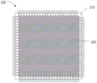
Fig. 2 depicts a top view of a grid connector according to an embodiment.
Fig. 3 depicts a top view of a print memory of a contact grid connector according to an embodiment.
Fig. 4 depicts an enlarged top view of a portion of fig. 3, according to an embodiment.
Fig. 5 depicts a cross-sectional side view of a portion of a print memory contacting a portion of a grid connector according to an embodiment.
Fig. 6 depicts a flowchart of a method for transferring data between a print memory and a grid connector according to an embodiment.
FIG. 7 depicts a computing system for performing at least a portion of a method according to an embodiment.
Detailed Description
Reference will now be made to exemplary embodiments of the present teachings, examples of which are illustrated in the accompanying drawings. Wherever possible, the same reference numbers will be used throughout the drawings to refer to the same, like, or similar parts.
Fig. 1 depicts a top view of a print memory 100 according to an embodiment. Print memory 100 may include a thin flexible substrate 110. Substrate 110 may include a rewritable memory. For example, rewritable memory may include 36 bits, which may store up to approximately 680 hundred million data points.
Fig. 2 depicts a top view of a grid connector 200 according to an embodiment. Grid connector 200 may be part of (e.g., coupled with) a data transfer device for communicating with print memory 100. More specifically, grid connector 200 may be configured to transmit (i.e., write) data to print memory 100 and/or receive (i.e., read) data from print memory 100. The grid connector 200 may include a thin substrate 210. Substrate 210 may be made of silicon. The grid connector 200 (e.g., substrate 210) may be used as a mechanical interface between the print memory 100 and the computing system of the data transfer device (see fig. 7).
The grid connector 200 may also include a plurality of conductive pads 220. The conductive pad 220 may be made of a metal or a metal alloy. The conductive pads 220 may protrude outward with respect to the upper/outer surface of the substrate 210.
Fig. 3 depicts a top view of the print memory 100 of the contact grid connector 200, and fig. 4 depicts an enlarged top view of a portion of fig. 3, according to an embodiment. More specifically, fig. 3 and 4 depict a face-down printing memory 100 in which the conductive pads 120A, 120B contact the conductive pads 220 of the face-up grid connector 200. Print memory 100 is shown as transparent in fig. 3 and 4.
The substrate 110 of the print memory 100 may have a smaller surface area than the substrate 210 of the grid connector 200. The conductive pads 120A, 120B of the print memory 100 may each have a larger surface area than the conductive pads 220 of the connector 200. Therefore, compared with the traditional spring-loaded spring thimble, Connectors, leaf spring connectors, and the like, the conductive pads (e.g., plurality of conductive pads) 220 of the
 grid connector 200 may be aligned with and in physical contact with each conductive pad 120A, 120B of the print memory 100 regardless of the position and/or orientation of the print memory 110 relative to the grid connector 200. In other words, the print memory 100 may move and/or rotate relative to the grid connector 200, and the conductive pads (e.g., a plurality of conductive pads) 220 of the grid connector 200 may align with and physically contact each conductive pad 120A, 120B of the print memory 100 as long as the conductive pads 120A, 120B of the print memory 100 remain within the circumference/boundary 224 of the conductive pads 220 of the grid connector 200.
The conductive pads 220 of the grid connector 200 that are in contact with the conductive pads 120A, 120B of the print memory 100 may provide an electrical connection between each other (e.g., through the conductive pads 120A, 120B). However, the conductive pads 220 of the grid connector 200 that are not in contact with the conductive pads 120A, 120B of the print memory 100 may not provide an electrical connection between each other. As explained in more detail below, this may allow a computing system in the data transfer device (see fig. 7) to determine/identify the subset of conductive pads 220 of the grid connector 200 that are in contact with the conductive pads 120A, 120B of the print memory 100. Each subset may include a plurality of conductive pads 220 (e.g., from about 5 to about 30 or about 10 to about 20).
Once the subset of conductive pads 220 in contact with the conductive pads 120A, 120B of the print memory 100 is identified, the computing system may also determine/identify conductive pads 220 in the subset that are located within a predetermined distance of the boundary 124 of the conductive pads 120A, 120B. For example, the boundary conductive pad may be aligned with the boundary 124 of the conductive pads 120A, 120B or at least partially overlap the boundary 124. Accordingly, contact between the boundary conductive pad and the conductive pads 120A, 120B may be less reliable than a conductive pad 220 positioned within the boundary 124 and greater than a predetermined distance from the boundary 124.
When the conductive pads 120A, 120B of the print memory 100 are in contact with the conductive pads 220 of the grid connector 200, data may be transferred between the print memory 100 and the grid connector 200. More specifically, digital data may be transmitted from grid connector 200 through conductive pads 120A, 120B, 220 and stored in a rewritable memory in substrate 110 of print memory 100 (e.g., as part of a write function). Alternatively, digital data may be transferred from a rewritable memory in the substrate 110 to the grid connector 200 (e.g., as part of a read function) via the conductive pads 120A, 120B, 220.
The data transmitted through the conductive patch 120A may be or include information about the product to which the print memory 100 is coupled (e.g., adhered). For example, the data may be or include the date of manufacture of the product, the location where the product was manufactured, the expiration date of the product, and the like. Print memory 100 may also track operational data of the travel of the system. This works when the print memory 100 is attached to a subsystem or sub-component of a larger system. For example, the print memory 100 may record the number of copies a print cartridge (e.g., subsystem) has made in a copier machine (e.g., a larger system), record how much water has passed through a filter in a refrigerator, record how many failures have occurred while the subsystem is operating in any number of larger systems, and so forth. The data may also be or include encrypted data to prevent counterfeiting of the product. The conductive pads 120B may enable a data transfer device (of which the grid connector 200 is a part) to determine the position and/or orientation of each of the conductive pads 120A of the print memory 100 relative to the print memory 100 and/or the grid connector 200. In at least one embodiment, the data transmitted through conductive patch 120A may not include position/orientation information and conductive patch 120B may not include information about the product to which print memory 100 is coupled.
Fig. 5 depicts a cross-sectional side view of a portion of the print memory 100 contacting a portion of the grid connector 200 according to an embodiment. The conductive pads 120A, 120B may be positioned within recesses in the substrate 110. The upper/outer surfaces 122 of the conductive pads 120A, 120B may be recessed a distance relative to the upper/outer surface 112 of the substrate 110. The distance may be, for example, about 0.001 inches.
The conductive pads 220 of the grid connector 200 may protrude a distance outward from the upper/outer surface 212 of the substrate 210. The distance may be, for example, about 0.005 inches. This may allow the conductive pads 220 of the grid connector 200 to contact the recessed conductive pads 120A, 120B of the print memory 100.
Fig. 6 depicts a flowchart of a method 600 for transferring data between the print memory 100 and the grid connector 200 according to an embodiment. The method 600 may include placing the grid connector 200 in contact with the print memory 100, as at 602. More specifically, the plurality of conductive pads 220 of the grid connector 200 may be disposed in contact with each of the conductive pads 120A, 120B of the print memory 100.
The method 600 may also include identifying a subset of the conductive pads 220 of the grid connector 200 that are in contact with the conductive pads 120A, 120B of the print memory 100 at 604. More specifically, the computing system (see fig. 7) may identify the subgroups by determining that the conductive pads 220 in the subgroup have an electrical connection with each other. The method 600 may also include identifying the conductive pads 220 in the subset within the predetermined distance of the boundary 124 of each conductive pad 120A, 120B at 606.
The method 600 may also include transferring data between the print memory 100 and the grid connector 200 at 608. More specifically, data may be transferred between the conductive pads 120A, 120B of the print memory 100 and the subset of conductive pads 220 of the grid connector 200. In at least one embodiment, data may not be transmitted through the conductive pads 220 in the subset within the predetermined distance of the boundary 124 of each conductive pad 120A, 120B.
Fig. 7 illustrates an example of such a computing system 700, according to some embodiments. The computing system 700 may be part of a data transfer device and thus communicate with the grid connector 200. Computing system 700 may include a computer or computer system 701A, which may be a standalone computer system 701A or a distributed computer system arrangement. Computer system 701A includes one or more analysis modules 702 configured to perform various tasks according to some embodiments, such as one or more methods disclosed herein. To perform these various tasks, analysis module 702 executes independently or in conjunction with one or more processors 704, the one or more processors 704 connected to one or more storage media 706. Processor 704 is also connected to network interface 707 to allow computer system 701A to communicate with one or more additional computer systems and/or computing systems, such as 701B, 701C, and/or 701D, over data network 709 (note that computer systems 701B, 701C, and/or 701D may or may not share the same structure with computer system 701A and may be located in different physical locations, e.g., computer systems 701A and 701B may be located in a processing facility while communicating with one or more computer systems, such as 701C and/or 701D, located in one or more data centers and/or different countries located on different continents).
A processor may include a microprocessor, microcontroller, processor module or subsystem, programmable integrated circuit, programmable gate array, or another control or computing device.
The storage medium 706 may be embodied as one or more computer-readable or machine-readable storage media. It is noted that although the storage medium 706 is depicted as being within the computer system 701A in the example embodiment of fig. 7, in some embodiments the storage medium 706 may be distributed within and/or across multiple internal and/or external cartridge modules of the computing system 701A and/or additional computing systems. The storage medium 706 may include one or more of various forms of memory, including semiconductor memory devices, such as dynamic or static random access memory (DRAM or SRAM), Erasable and Programmable Read Only Memory (EPROM), Electrically Erasable and Programmable Read Only Memory (EEPROM), and flash memory; magnetic disks such as fixed, floppy, and removable disks; another magnetic medium comprising a tape; such as Compact Discs (CDs) or Digital Video Discs (DVDs), An optical medium such as a magnetic disk or another type of optical storage; or other type of storage device. Note that the instructions described above may be provided on one computer-readable or machine-readable storage medium, or may be provided on multiple computer-readable or machine-readable storage media distributed in a large system, which may have multiple nodes. The computer-readable or machine-readable storage medium or media is considered to be part of an article (or article of manufacture). An article or article may refer to any manufactured single or multiple parts. The storage medium or media may be located in a machine that executes machine-readable instructions or at a remote location from where the machine-readable instructions may be downloaded for execution over a network.
In some embodiments, computing system 700 includes one or more data transfer modules 708. In the example of computing system 700, computer system 701A includes a data transfer module 708. In some embodiments, a single data transfer module may be used to perform at least some aspects of one or more embodiments of method 600. In other embodiments, multiple data transmission modules may be used to perform at least some aspects of method 600.
It should be understood that computing system 700 is one example of a computing system, and that computing system 700 may have more or fewer components than illustrated, may incorporate additional components not described in the example embodiment of fig. 7, and/or that computing system 700 may have a different configuration or arrangement of components depicted in fig. 7. The various components shown in fig. 7 may be implemented in hardware, software, or a combination of both hardware and software, including one or more signal processing and/or application specific integrated circuits.
In addition, the steps in the processing methods described herein may be implemented by running one or more functional blocks in an information processing apparatus, such as a general purpose processor or a special purpose chip, such as an ASIC, FPGA, PLD, or other suitable device. These modules, combinations of these modules and/or their combination with general hardware are included within the scope of the present invention.
Notwithstanding that the numerical ranges and parameters setting forth the broad scope of the present teachings are approximations, the numerical values set forth in the specific examples are reported as precisely as possible. Any numerical value, however, inherently contains certain errors necessarily resulting from the standard deviation found in their respective testing measurements. Moreover, all ranges disclosed herein are to be understood to encompass any and all subranges subsumed therein. For example, a range of "less than 10" can include any and all subranges between (and including) the minimum value of zero and the maximum value of 10, i.e., any and all subranges having a minimum value equal to or greater than zero and a maximum value of equal to or less than 10, e.g., 1 to 5.
Claims (20)
1. A grid connector for communicating with a print memory, comprising:
a substrate; and
a plurality of first conductive pads coupled to the substrate, wherein each of the first conductive pads protrudes outward relative to an outer surface of the substrate, and wherein a subset of the first conductive pads are configured to directly contact a second conductive pad of the print memory to allow data to be transferred between the grid connector and the print memory when the grid connector is in a 1:1 alignment relative to the print memory or at any other angle relative to the print memory that is independent of an orientation of the print memory as long as the second conductive pad is within a boundary of the first conductive pad.
2. The grid connector of claim 1, wherein the grid connector is configured to transmit the data to the print memory when the subset of the first conductive pads contacts the second conductive pads, and wherein the grid connector is configured to receive the data from the print memory when the subset of the first conductive pads contacts the second conductive pads.
3. The grid connector of claim 2, wherein the subset includes two or more of the first conductive pads.
4. The grid connector of claim 3, wherein the first conductive pads of the subset are electrically connected to each other when the first conductive pads of the subset are in contact with the second conductive pads of the printed memory.
5. The grid connector of claim 3, wherein the first conductive pads not in the subset are not electrically connected to each other when the first conductive pads in the subset are in contact with the second conductive pads of the printed memory.
6. A system for communicating with a print memory, comprising:
a print memory, the print memory comprising:
a first substrate; and
a plurality of first conductive pads coupled to the first substrate, wherein each of the first conductive pads is recessed relative to an outer surface of the first substrate;
a grid connector, the grid connector comprising:
a second substrate; and
a plurality of second conductive pads coupled to the second substrate, wherein each of the second conductive pads protrudes outward relative to an outer surface of the second substrate, wherein a different subset of the second conductive pads is configured to directly contact each of the first conductive pads to allow data to be transferred between the grid connector and the print memory when the grid connector is in a 1:1 alignment relative to the print memory or at any other angle relative to the print memory that is independent of an orientation of the print memory as long as the first conductive pads are within a boundary of the second conductive pads, and wherein each subset includes two or more of the second conductive pads; and a computing system in communication with the grid connector, wherein the computing system is configured to communicate with the print memory via the grid connector when the different subset of the second conductive pads are in direct contact with each of the first conductive pads.
7. The system of claim 6, wherein the computing system is configured to identify the subset of the second conductive pads that are in contact with the first conductive pad by determining that the second conductive pads in the subset are electrically connected to each other.
8. The system of claim 7, wherein the computing system is configured to identify the second conductive patch of the subset that is within a predetermined distance of a boundary of each of the first conductive patches.
9. The system of claim 8, wherein the computing system is configured to communicate with the print memory via the grid connector through a second conductive pad of the subset except for the second conductive pad of the subset that is located within the predetermined distance of the boundary of each of the first conductive pads.
10. The system of claim 6, wherein the data transmitted through one of the first conductive pads comprises information about a product to which the print memory is configured to be coupled, and wherein the data transmitted through another one of the first conductive pads comprises information about a location of the one of the first conductive pads.
11. A method for communicating with a print memory, comprising:
placing a grid connector in direct contact with the print memory, wherein the print memory comprises a first conductive pad, wherein the grid connector comprises a plurality of second conductive pads, and wherein placing the grid connector in direct contact with the print memory comprises placing a subset of the second conductive pads of the grid connector in direct contact with the first conductive pads of the print memory when the grid connector is in a 1:1 alignment with respect to the print memory or at any other angle with respect to the print memory that is independent of the orientation of the print memory so long as the first conductive pads are within the boundaries of the second conductive pads; and
transferring data between the first conductive pads of the print memory and the subset of the second conductive pads of the grid connector.
12. The method of claim 11, wherein the subset includes two or more of the second conductive pads.
13. The method of claim 12, further comprising identifying the subset of the second conductive pads that are in contact with the first conductive pad by determining that the second conductive pads in the subset are electrically connected to each other.
14. The method of claim 13, further comprising identifying the second conductive pad in the subset that is within a predetermined distance of a boundary of the first conductive pad.
15. The method of claim 14, further comprising transmitting the data between the first conductive pads of the print memory and the subset of the second conductive pads of the grid connector that are not within the predetermined distance of the boundary, wherein the data is not transmitted through the second conductive pads of the subset that are within the predetermined distance of the boundary.
16. The method of claim 14, wherein at least a portion of the second conductive pads that are not part of the subset are not electrically connected to each other.
17. The method of claim 14, further comprising determining a position, an orientation, or both, of the print memory relative to the grid connector.
18. The method of claim 14, further comprising determining a position, an orientation, or both, of the first conductive pad relative to the print memory.
19. The method of claim 14, further comprising determining a position, an orientation, or both, of the first conductive pad relative to the grid connector.
20. The method of claim 14, wherein the data transmitted through the first conductive patch includes information about a product to which the print memory is to be coupled, wherein the print memory further includes a third conductive patch for determining a location, an orientation, or both, of the first conductive patch on the print memory, wherein the data transmitted through the first conductive patch does not include information about the location, the orientation, or both, and wherein the third conductive patch does not include information about the product.
Applications Claiming Priority (2)
| Application Number | Priority Date | Filing Date | Title |
|---|---|---|---|
| US15/498219 | 2017-04-26 | ||
| US15/498,219 US10319415B2 (en) | 2017-04-26 | 2017-04-26 | Printed memory grid connector |
Publications (2)
| Publication Number | Publication Date |
|---|---|
| CN108804049A CN108804049A (en) | 2018-11-13 |
| CN108804049B true CN108804049B (en) | 2021-01-05 |
Family
ID=62062796
Family Applications (1)
| Application Number | Title | Priority Date | Filing Date |
|---|---|---|---|
| CN201810313374.7A Active CN108804049B (en) | 2017-04-26 | 2018-04-09 | Print memory grid connector |
Country Status (5)
| Country | Link |
|---|---|
| US (1) | US10319415B2 (en) |
| EP (1) | EP3422021B1 (en) |
| JP (1) | JP6978372B2 (en) |
| KR (1) | KR102319948B1 (en) |
| CN (1) | CN108804049B (en) |
Families Citing this family (1)
| Publication number | Priority date | Publication date | Assignee | Title |
|---|---|---|---|---|
| US20070093157A1 (en) | 2005-10-20 | 2007-04-26 | Kimberly-Clark Worldwide, Inc. | High speed, pressure bonded, thin sheet laminate |
Citations (4)
| Publication number | Priority date | Publication date | Assignee | Title |
|---|---|---|---|---|
| CN102164462A (en) * | 2010-02-22 | 2011-08-24 | 佳明瑞士有限责任公司 | Methods for memory programming during product assembly |
| CN105659255A (en) * | 2013-08-28 | 2016-06-08 | 惠普发展公司,有限责任合伙企业 | Cartridge comprising an auto-destruct feature |
| CN105788642A (en) * | 2015-01-11 | 2016-07-20 | 杭州海存信息技术有限公司 | Solid state compact disc and solid storage server |
| CN105975644A (en) * | 2015-03-13 | 2016-09-28 | 三星电子株式会社 | Methods, systems, and computer program products providing layout data for integrated circuits |
Family Cites Families (6)
| Publication number | Priority date | Publication date | Assignee | Title |
|---|---|---|---|---|
| US6174175B1 (en) * | 1999-04-29 | 2001-01-16 | International Business Machines Corporation | High density Z-axis connector |
| US20080225476A1 (en) | 2006-01-11 | 2008-09-18 | Chris Karabatsos | Tab wrap foldable electronic assembly module and method of manufacture |
| US8381601B2 (en) * | 2008-05-05 | 2013-02-26 | John F. Stumpf | Transducer matrix film |
| KR101467469B1 (en) * | 2013-04-03 | 2014-12-02 | (주) 파루 | Printed memory circuit apparatus and rfid tag thereof |
| KR102218743B1 (en) | 2014-08-01 | 2021-02-22 | 삼성전자주식회사 | Integrated circuit card socket |
| US10114984B2 (en) * | 2015-09-04 | 2018-10-30 | Xerox Corporation | Symmetric bit coding for printed memory devices |
-
2017
- 2017-04-26 US US15/498,219 patent/US10319415B2/en active Active
-
2018
- 2018-04-04 JP JP2018072205A patent/JP6978372B2/en active Active
- 2018-04-05 EP EP18165989.7A patent/EP3422021B1/en active Active
- 2018-04-09 KR KR1020180041049A patent/KR102319948B1/en active IP Right Grant
- 2018-04-09 CN CN201810313374.7A patent/CN108804049B/en active Active
Patent Citations (4)
| Publication number | Priority date | Publication date | Assignee | Title |
|---|---|---|---|---|
| CN102164462A (en) * | 2010-02-22 | 2011-08-24 | 佳明瑞士有限责任公司 | Methods for memory programming during product assembly |
| CN105659255A (en) * | 2013-08-28 | 2016-06-08 | 惠普发展公司,有限责任合伙企业 | Cartridge comprising an auto-destruct feature |
| CN105788642A (en) * | 2015-01-11 | 2016-07-20 | 杭州海存信息技术有限公司 | Solid state compact disc and solid storage server |
| CN105975644A (en) * | 2015-03-13 | 2016-09-28 | 三星电子株式会社 | Methods, systems, and computer program products providing layout data for integrated circuits |
Also Published As
| Publication number | Publication date |
|---|---|
| JP2018186080A (en) | 2018-11-22 |
| EP3422021A1 (en) | 2019-01-02 |
| JP6978372B2 (en) | 2021-12-08 |
| EP3422021B1 (en) | 2020-06-10 |
| KR20180120082A (en) | 2018-11-05 |
| CN108804049A (en) | 2018-11-13 |
| US20180315456A1 (en) | 2018-11-01 |
| US10319415B2 (en) | 2019-06-11 |
| KR102319948B1 (en) | 2021-10-29 |
Similar Documents
| Publication | Publication Date | Title |
|---|---|---|
| CN107766172B (en) | DRAM auxiliary error correction method for DDR SDRAM interface | |
| US9934825B2 (en) | Semiconductor device and electronic device | |
| US20090063895A1 (en) | Scaleable and maintainable solid state drive | |
| CN107015890B (en) | Storage device, server system having the same, and method of operating the same | |
| TWI569152B (en) | Communicating over portions of a communication medium | |
| US20070050689A1 (en) | Storage system comprising logical circuit configured in accordance with information in memory on PLD | |
| JP6545630B2 (en) | Wireless data concentrator for aircraft data networks | |
| US9024426B2 (en) | Semiconductor device and method of manufacturing the same | |
| CN108804049B (en) | Print memory grid connector | |
| US9570446B1 (en) | Semiconductor device | |
| US20210334414A1 (en) | Storage device and solid state drive device with structure for improving security performance and removing data, method of operating the same, and data center including the same | |
| US9063827B2 (en) | Systems and methods for storing and retrieving a defect map in a DRAM component | |
| US20170228179A1 (en) | Method and apparatus for providing increased storage capacity | |
| KR20230161375A (en) | Systems and methods for expandable memory error handling | |
| US6560733B1 (en) | Soft error detection for digital signal processors | |
| US9520162B2 (en) | DIMM device controller supervisor | |
| US11023247B2 (en) | Processor package with optimization based on package connection type | |
| KR20230030795A (en) | Memory controller and the memory device comprising the same | |
| CN115083453A (en) | Storage device with separate power supply capabilities | |
| US10761747B2 (en) | Memory device and memory system including the same | |
| US20030103462A1 (en) | IBIST interconnect and bridge fault detection scheme | |
| CN113496745A (en) | Apparatus and method for repairing defect of memory module and memory system | |
| US20130007362A1 (en) | Method and system of detecting redundant array of independent disks and transferring data | |
| EP4180965A1 (en) | Storage devices configured to obtain data of external devices for debugging | |
| CN117093390A (en) | System for processing faulty page, method for processing faulty page, and host device |
Legal Events
| Date | Code | Title | Description |
|---|---|---|---|
| PB01 | Publication | ||
| PB01 | Publication | ||
| SE01 | Entry into force of request for substantive examination | ||
| SE01 | Entry into force of request for substantive examination | ||
| GR01 | Patent grant | ||
| GR01 | Patent grant |