CN108642474B - Substrate processing system for depositing a film on a substrate - Google Patents
Substrate processing system for depositing a film on a substrate Download PDFInfo
- Publication number
- CN108642474B CN108642474B CN201810478814.4A CN201810478814A CN108642474B CN 108642474 B CN108642474 B CN 108642474B CN 201810478814 A CN201810478814 A CN 201810478814A CN 108642474 B CN108642474 B CN 108642474B
- Authority
- CN
- China
- Prior art keywords
- substrate
- backside
- purge
- gas
- film
- Prior art date
- Legal status (The legal status is an assumption and is not a legal conclusion. Google has not performed a legal analysis and makes no representation as to the accuracy of the status listed.)
- Active
Links
Images


Classifications
-
- C—CHEMISTRY; METALLURGY
- C23—COATING METALLIC MATERIAL; COATING MATERIAL WITH METALLIC MATERIAL; CHEMICAL SURFACE TREATMENT; DIFFUSION TREATMENT OF METALLIC MATERIAL; COATING BY VACUUM EVAPORATION, BY SPUTTERING, BY ION IMPLANTATION OR BY CHEMICAL VAPOUR DEPOSITION, IN GENERAL; INHIBITING CORROSION OF METALLIC MATERIAL OR INCRUSTATION IN GENERAL
- C23C—COATING METALLIC MATERIAL; COATING MATERIAL WITH METALLIC MATERIAL; SURFACE TREATMENT OF METALLIC MATERIAL BY DIFFUSION INTO THE SURFACE, BY CHEMICAL CONVERSION OR SUBSTITUTION; COATING BY VACUUM EVAPORATION, BY SPUTTERING, BY ION IMPLANTATION OR BY CHEMICAL VAPOUR DEPOSITION, IN GENERAL
- C23C16/00—Chemical coating by decomposition of gaseous compounds, without leaving reaction products of surface material in the coating, i.e. chemical vapour deposition [CVD] processes
- C23C16/44—Chemical coating by decomposition of gaseous compounds, without leaving reaction products of surface material in the coating, i.e. chemical vapour deposition [CVD] processes characterised by the method of coating
- C23C16/455—Chemical coating by decomposition of gaseous compounds, without leaving reaction products of surface material in the coating, i.e. chemical vapour deposition [CVD] processes characterised by the method of coating characterised by the method used for introducing gases into reaction chamber or for modifying gas flows in reaction chamber
- C23C16/45597—Reactive back side gas
-
- C—CHEMISTRY; METALLURGY
- C23—COATING METALLIC MATERIAL; COATING MATERIAL WITH METALLIC MATERIAL; CHEMICAL SURFACE TREATMENT; DIFFUSION TREATMENT OF METALLIC MATERIAL; COATING BY VACUUM EVAPORATION, BY SPUTTERING, BY ION IMPLANTATION OR BY CHEMICAL VAPOUR DEPOSITION, IN GENERAL; INHIBITING CORROSION OF METALLIC MATERIAL OR INCRUSTATION IN GENERAL
- C23C—COATING METALLIC MATERIAL; COATING MATERIAL WITH METALLIC MATERIAL; SURFACE TREATMENT OF METALLIC MATERIAL BY DIFFUSION INTO THE SURFACE, BY CHEMICAL CONVERSION OR SUBSTITUTION; COATING BY VACUUM EVAPORATION, BY SPUTTERING, BY ION IMPLANTATION OR BY CHEMICAL VAPOUR DEPOSITION, IN GENERAL
- C23C16/00—Chemical coating by decomposition of gaseous compounds, without leaving reaction products of surface material in the coating, i.e. chemical vapour deposition [CVD] processes
- C23C16/22—Chemical coating by decomposition of gaseous compounds, without leaving reaction products of surface material in the coating, i.e. chemical vapour deposition [CVD] processes characterised by the deposition of inorganic material, other than metallic material
- C23C16/30—Deposition of compounds, mixtures or solid solutions, e.g. borides, carbides, nitrides
- C23C16/34—Nitrides
- C23C16/345—Silicon nitride
-
- C—CHEMISTRY; METALLURGY
- C23—COATING METALLIC MATERIAL; COATING MATERIAL WITH METALLIC MATERIAL; CHEMICAL SURFACE TREATMENT; DIFFUSION TREATMENT OF METALLIC MATERIAL; COATING BY VACUUM EVAPORATION, BY SPUTTERING, BY ION IMPLANTATION OR BY CHEMICAL VAPOUR DEPOSITION, IN GENERAL; INHIBITING CORROSION OF METALLIC MATERIAL OR INCRUSTATION IN GENERAL
- C23C—COATING METALLIC MATERIAL; COATING MATERIAL WITH METALLIC MATERIAL; SURFACE TREATMENT OF METALLIC MATERIAL BY DIFFUSION INTO THE SURFACE, BY CHEMICAL CONVERSION OR SUBSTITUTION; COATING BY VACUUM EVAPORATION, BY SPUTTERING, BY ION IMPLANTATION OR BY CHEMICAL VAPOUR DEPOSITION, IN GENERAL
- C23C16/00—Chemical coating by decomposition of gaseous compounds, without leaving reaction products of surface material in the coating, i.e. chemical vapour deposition [CVD] processes
- C23C16/22—Chemical coating by decomposition of gaseous compounds, without leaving reaction products of surface material in the coating, i.e. chemical vapour deposition [CVD] processes characterised by the deposition of inorganic material, other than metallic material
- C23C16/30—Deposition of compounds, mixtures or solid solutions, e.g. borides, carbides, nitrides
- C23C16/40—Oxides
- C23C16/401—Oxides containing silicon
- C23C16/402—Silicon dioxide
-
- C—CHEMISTRY; METALLURGY
- C23—COATING METALLIC MATERIAL; COATING MATERIAL WITH METALLIC MATERIAL; CHEMICAL SURFACE TREATMENT; DIFFUSION TREATMENT OF METALLIC MATERIAL; COATING BY VACUUM EVAPORATION, BY SPUTTERING, BY ION IMPLANTATION OR BY CHEMICAL VAPOUR DEPOSITION, IN GENERAL; INHIBITING CORROSION OF METALLIC MATERIAL OR INCRUSTATION IN GENERAL
- C23C—COATING METALLIC MATERIAL; COATING MATERIAL WITH METALLIC MATERIAL; SURFACE TREATMENT OF METALLIC MATERIAL BY DIFFUSION INTO THE SURFACE, BY CHEMICAL CONVERSION OR SUBSTITUTION; COATING BY VACUUM EVAPORATION, BY SPUTTERING, BY ION IMPLANTATION OR BY CHEMICAL VAPOUR DEPOSITION, IN GENERAL
- C23C16/00—Chemical coating by decomposition of gaseous compounds, without leaving reaction products of surface material in the coating, i.e. chemical vapour deposition [CVD] processes
- C23C16/22—Chemical coating by decomposition of gaseous compounds, without leaving reaction products of surface material in the coating, i.e. chemical vapour deposition [CVD] processes characterised by the deposition of inorganic material, other than metallic material
- C23C16/30—Deposition of compounds, mixtures or solid solutions, e.g. borides, carbides, nitrides
- C23C16/40—Oxides
- C23C16/405—Oxides of refractory metals or yttrium
-
- C—CHEMISTRY; METALLURGY
- C23—COATING METALLIC MATERIAL; COATING MATERIAL WITH METALLIC MATERIAL; CHEMICAL SURFACE TREATMENT; DIFFUSION TREATMENT OF METALLIC MATERIAL; COATING BY VACUUM EVAPORATION, BY SPUTTERING, BY ION IMPLANTATION OR BY CHEMICAL VAPOUR DEPOSITION, IN GENERAL; INHIBITING CORROSION OF METALLIC MATERIAL OR INCRUSTATION IN GENERAL
- C23C—COATING METALLIC MATERIAL; COATING MATERIAL WITH METALLIC MATERIAL; SURFACE TREATMENT OF METALLIC MATERIAL BY DIFFUSION INTO THE SURFACE, BY CHEMICAL CONVERSION OR SUBSTITUTION; COATING BY VACUUM EVAPORATION, BY SPUTTERING, BY ION IMPLANTATION OR BY CHEMICAL VAPOUR DEPOSITION, IN GENERAL
- C23C16/00—Chemical coating by decomposition of gaseous compounds, without leaving reaction products of surface material in the coating, i.e. chemical vapour deposition [CVD] processes
- C23C16/44—Chemical coating by decomposition of gaseous compounds, without leaving reaction products of surface material in the coating, i.e. chemical vapour deposition [CVD] processes characterised by the method of coating
- C23C16/455—Chemical coating by decomposition of gaseous compounds, without leaving reaction products of surface material in the coating, i.e. chemical vapour deposition [CVD] processes characterised by the method of coating characterised by the method used for introducing gases into reaction chamber or for modifying gas flows in reaction chamber
- C23C16/45523—Pulsed gas flow or change of composition over time
- C23C16/45525—Atomic layer deposition [ALD]
- C23C16/45527—Atomic layer deposition [ALD] characterized by the ALD cycle, e.g. different flows or temperatures during half-reactions, unusual pulsing sequence, use of precursor mixtures or auxiliary reactants or activations
- C23C16/45536—Use of plasma, radiation or electromagnetic fields
-
- C—CHEMISTRY; METALLURGY
- C23—COATING METALLIC MATERIAL; COATING MATERIAL WITH METALLIC MATERIAL; CHEMICAL SURFACE TREATMENT; DIFFUSION TREATMENT OF METALLIC MATERIAL; COATING BY VACUUM EVAPORATION, BY SPUTTERING, BY ION IMPLANTATION OR BY CHEMICAL VAPOUR DEPOSITION, IN GENERAL; INHIBITING CORROSION OF METALLIC MATERIAL OR INCRUSTATION IN GENERAL
- C23C—COATING METALLIC MATERIAL; COATING MATERIAL WITH METALLIC MATERIAL; SURFACE TREATMENT OF METALLIC MATERIAL BY DIFFUSION INTO THE SURFACE, BY CHEMICAL CONVERSION OR SUBSTITUTION; COATING BY VACUUM EVAPORATION, BY SPUTTERING, BY ION IMPLANTATION OR BY CHEMICAL VAPOUR DEPOSITION, IN GENERAL
- C23C16/00—Chemical coating by decomposition of gaseous compounds, without leaving reaction products of surface material in the coating, i.e. chemical vapour deposition [CVD] processes
- C23C16/44—Chemical coating by decomposition of gaseous compounds, without leaving reaction products of surface material in the coating, i.e. chemical vapour deposition [CVD] processes characterised by the method of coating
- C23C16/455—Chemical coating by decomposition of gaseous compounds, without leaving reaction products of surface material in the coating, i.e. chemical vapour deposition [CVD] processes characterised by the method of coating characterised by the method used for introducing gases into reaction chamber or for modifying gas flows in reaction chamber
- C23C16/45523—Pulsed gas flow or change of composition over time
- C23C16/45525—Atomic layer deposition [ALD]
- C23C16/45544—Atomic layer deposition [ALD] characterized by the apparatus
-
- C—CHEMISTRY; METALLURGY
- C23—COATING METALLIC MATERIAL; COATING MATERIAL WITH METALLIC MATERIAL; CHEMICAL SURFACE TREATMENT; DIFFUSION TREATMENT OF METALLIC MATERIAL; COATING BY VACUUM EVAPORATION, BY SPUTTERING, BY ION IMPLANTATION OR BY CHEMICAL VAPOUR DEPOSITION, IN GENERAL; INHIBITING CORROSION OF METALLIC MATERIAL OR INCRUSTATION IN GENERAL
- C23C—COATING METALLIC MATERIAL; COATING MATERIAL WITH METALLIC MATERIAL; SURFACE TREATMENT OF METALLIC MATERIAL BY DIFFUSION INTO THE SURFACE, BY CHEMICAL CONVERSION OR SUBSTITUTION; COATING BY VACUUM EVAPORATION, BY SPUTTERING, BY ION IMPLANTATION OR BY CHEMICAL VAPOUR DEPOSITION, IN GENERAL
- C23C16/00—Chemical coating by decomposition of gaseous compounds, without leaving reaction products of surface material in the coating, i.e. chemical vapour deposition [CVD] processes
- C23C16/44—Chemical coating by decomposition of gaseous compounds, without leaving reaction products of surface material in the coating, i.e. chemical vapour deposition [CVD] processes characterised by the method of coating
- C23C16/458—Chemical coating by decomposition of gaseous compounds, without leaving reaction products of surface material in the coating, i.e. chemical vapour deposition [CVD] processes characterised by the method of coating characterised by the method used for supporting substrates in the reaction chamber
- C23C16/4582—Rigid and flat substrates, e.g. plates or discs
- C23C16/4583—Rigid and flat substrates, e.g. plates or discs the substrate being supported substantially horizontally
- C23C16/4585—Devices at or outside the perimeter of the substrate support, e.g. clamping rings, shrouds
-
- C—CHEMISTRY; METALLURGY
- C23—COATING METALLIC MATERIAL; COATING MATERIAL WITH METALLIC MATERIAL; CHEMICAL SURFACE TREATMENT; DIFFUSION TREATMENT OF METALLIC MATERIAL; COATING BY VACUUM EVAPORATION, BY SPUTTERING, BY ION IMPLANTATION OR BY CHEMICAL VAPOUR DEPOSITION, IN GENERAL; INHIBITING CORROSION OF METALLIC MATERIAL OR INCRUSTATION IN GENERAL
- C23C—COATING METALLIC MATERIAL; COATING MATERIAL WITH METALLIC MATERIAL; SURFACE TREATMENT OF METALLIC MATERIAL BY DIFFUSION INTO THE SURFACE, BY CHEMICAL CONVERSION OR SUBSTITUTION; COATING BY VACUUM EVAPORATION, BY SPUTTERING, BY ION IMPLANTATION OR BY CHEMICAL VAPOUR DEPOSITION, IN GENERAL
- C23C16/00—Chemical coating by decomposition of gaseous compounds, without leaving reaction products of surface material in the coating, i.e. chemical vapour deposition [CVD] processes
- C23C16/44—Chemical coating by decomposition of gaseous compounds, without leaving reaction products of surface material in the coating, i.e. chemical vapour deposition [CVD] processes characterised by the method of coating
- C23C16/50—Chemical coating by decomposition of gaseous compounds, without leaving reaction products of surface material in the coating, i.e. chemical vapour deposition [CVD] processes characterised by the method of coating using electric discharges
- C23C16/505—Chemical coating by decomposition of gaseous compounds, without leaving reaction products of surface material in the coating, i.e. chemical vapour deposition [CVD] processes characterised by the method of coating using electric discharges using radio frequency discharges
-
- C—CHEMISTRY; METALLURGY
- C23—COATING METALLIC MATERIAL; COATING MATERIAL WITH METALLIC MATERIAL; CHEMICAL SURFACE TREATMENT; DIFFUSION TREATMENT OF METALLIC MATERIAL; COATING BY VACUUM EVAPORATION, BY SPUTTERING, BY ION IMPLANTATION OR BY CHEMICAL VAPOUR DEPOSITION, IN GENERAL; INHIBITING CORROSION OF METALLIC MATERIAL OR INCRUSTATION IN GENERAL
- C23C—COATING METALLIC MATERIAL; COATING MATERIAL WITH METALLIC MATERIAL; SURFACE TREATMENT OF METALLIC MATERIAL BY DIFFUSION INTO THE SURFACE, BY CHEMICAL CONVERSION OR SUBSTITUTION; COATING BY VACUUM EVAPORATION, BY SPUTTERING, BY ION IMPLANTATION OR BY CHEMICAL VAPOUR DEPOSITION, IN GENERAL
- C23C16/00—Chemical coating by decomposition of gaseous compounds, without leaving reaction products of surface material in the coating, i.e. chemical vapour deposition [CVD] processes
- C23C16/44—Chemical coating by decomposition of gaseous compounds, without leaving reaction products of surface material in the coating, i.e. chemical vapour deposition [CVD] processes characterised by the method of coating
- C23C16/52—Controlling or regulating the coating process
-
- H—ELECTRICITY
- H01—ELECTRIC ELEMENTS
- H01J—ELECTRIC DISCHARGE TUBES OR DISCHARGE LAMPS
- H01J37/00—Discharge tubes with provision for introducing objects or material to be exposed to the discharge, e.g. for the purpose of examination or processing thereof
- H01J37/32—Gas-filled discharge tubes
- H01J37/32431—Constructional details of the reactor
- H01J37/3244—Gas supply means
- H01J37/32449—Gas control, e.g. control of the gas flow
-
- H—ELECTRICITY
- H01—ELECTRIC ELEMENTS
- H01J—ELECTRIC DISCHARGE TUBES OR DISCHARGE LAMPS
- H01J37/00—Discharge tubes with provision for introducing objects or material to be exposed to the discharge, e.g. for the purpose of examination or processing thereof
- H01J37/32—Gas-filled discharge tubes
- H01J37/32431—Constructional details of the reactor
- H01J37/32715—Workpiece holder
-
- H—ELECTRICITY
- H01—ELECTRIC ELEMENTS
- H01J—ELECTRIC DISCHARGE TUBES OR DISCHARGE LAMPS
- H01J37/00—Discharge tubes with provision for introducing objects or material to be exposed to the discharge, e.g. for the purpose of examination or processing thereof
- H01J37/32—Gas-filled discharge tubes
- H01J37/32431—Constructional details of the reactor
- H01J37/32798—Further details of plasma apparatus not provided for in groups H01J37/3244 - H01J37/32788; special provisions for cleaning or maintenance of the apparatus
- H01J37/32853—Hygiene
- H01J37/32871—Means for trapping or directing unwanted particles
-
- H—ELECTRICITY
- H01—ELECTRIC ELEMENTS
- H01L—SEMICONDUCTOR DEVICES NOT COVERED BY CLASS H10
- H01L21/00—Processes or apparatus adapted for the manufacture or treatment of semiconductor or solid state devices or of parts thereof
- H01L21/02—Manufacture or treatment of semiconductor devices or of parts thereof
- H01L21/02104—Forming layers
- H01L21/02107—Forming insulating materials on a substrate
- H01L21/02109—Forming insulating materials on a substrate characterised by the type of layer, e.g. type of material, porous/non-porous, pre-cursors, mixtures or laminates
- H01L21/02112—Forming insulating materials on a substrate characterised by the type of layer, e.g. type of material, porous/non-porous, pre-cursors, mixtures or laminates characterised by the material of the layer
- H01L21/02123—Forming insulating materials on a substrate characterised by the type of layer, e.g. type of material, porous/non-porous, pre-cursors, mixtures or laminates characterised by the material of the layer the material containing silicon
- H01L21/02164—Forming insulating materials on a substrate characterised by the type of layer, e.g. type of material, porous/non-porous, pre-cursors, mixtures or laminates characterised by the material of the layer the material containing silicon the material being a silicon oxide, e.g. SiO2
-
- H—ELECTRICITY
- H01—ELECTRIC ELEMENTS
- H01L—SEMICONDUCTOR DEVICES NOT COVERED BY CLASS H10
- H01L21/00—Processes or apparatus adapted for the manufacture or treatment of semiconductor or solid state devices or of parts thereof
- H01L21/02—Manufacture or treatment of semiconductor devices or of parts thereof
- H01L21/02104—Forming layers
- H01L21/02107—Forming insulating materials on a substrate
- H01L21/02109—Forming insulating materials on a substrate characterised by the type of layer, e.g. type of material, porous/non-porous, pre-cursors, mixtures or laminates
- H01L21/02112—Forming insulating materials on a substrate characterised by the type of layer, e.g. type of material, porous/non-porous, pre-cursors, mixtures or laminates characterised by the material of the layer
- H01L21/02123—Forming insulating materials on a substrate characterised by the type of layer, e.g. type of material, porous/non-porous, pre-cursors, mixtures or laminates characterised by the material of the layer the material containing silicon
- H01L21/0217—Forming insulating materials on a substrate characterised by the type of layer, e.g. type of material, porous/non-porous, pre-cursors, mixtures or laminates characterised by the material of the layer the material containing silicon the material being a silicon nitride not containing oxygen, e.g. SixNy or SixByNz
-
- H—ELECTRICITY
- H01—ELECTRIC ELEMENTS
- H01L—SEMICONDUCTOR DEVICES NOT COVERED BY CLASS H10
- H01L21/00—Processes or apparatus adapted for the manufacture or treatment of semiconductor or solid state devices or of parts thereof
- H01L21/02—Manufacture or treatment of semiconductor devices or of parts thereof
- H01L21/02104—Forming layers
- H01L21/02107—Forming insulating materials on a substrate
- H01L21/02109—Forming insulating materials on a substrate characterised by the type of layer, e.g. type of material, porous/non-porous, pre-cursors, mixtures or laminates
- H01L21/02112—Forming insulating materials on a substrate characterised by the type of layer, e.g. type of material, porous/non-porous, pre-cursors, mixtures or laminates characterised by the material of the layer
- H01L21/02172—Forming insulating materials on a substrate characterised by the type of layer, e.g. type of material, porous/non-porous, pre-cursors, mixtures or laminates characterised by the material of the layer the material containing at least one metal element, e.g. metal oxides, metal nitrides, metal oxynitrides or metal carbides
- H01L21/02175—Forming insulating materials on a substrate characterised by the type of layer, e.g. type of material, porous/non-porous, pre-cursors, mixtures or laminates characterised by the material of the layer the material containing at least one metal element, e.g. metal oxides, metal nitrides, metal oxynitrides or metal carbides characterised by the metal
- H01L21/02186—Forming insulating materials on a substrate characterised by the type of layer, e.g. type of material, porous/non-porous, pre-cursors, mixtures or laminates characterised by the material of the layer the material containing at least one metal element, e.g. metal oxides, metal nitrides, metal oxynitrides or metal carbides characterised by the metal the material containing titanium, e.g. TiO2
-
- H—ELECTRICITY
- H01—ELECTRIC ELEMENTS
- H01L—SEMICONDUCTOR DEVICES NOT COVERED BY CLASS H10
- H01L21/00—Processes or apparatus adapted for the manufacture or treatment of semiconductor or solid state devices or of parts thereof
- H01L21/02—Manufacture or treatment of semiconductor devices or of parts thereof
- H01L21/02104—Forming layers
- H01L21/02107—Forming insulating materials on a substrate
- H01L21/02225—Forming insulating materials on a substrate characterised by the process for the formation of the insulating layer
- H01L21/0226—Forming insulating materials on a substrate characterised by the process for the formation of the insulating layer formation by a deposition process
- H01L21/02263—Forming insulating materials on a substrate characterised by the process for the formation of the insulating layer formation by a deposition process deposition from the gas or vapour phase
- H01L21/02271—Forming insulating materials on a substrate characterised by the process for the formation of the insulating layer formation by a deposition process deposition from the gas or vapour phase deposition by decomposition or reaction of gaseous or vapour phase compounds, i.e. chemical vapour deposition
- H01L21/02274—Forming insulating materials on a substrate characterised by the process for the formation of the insulating layer formation by a deposition process deposition from the gas or vapour phase deposition by decomposition or reaction of gaseous or vapour phase compounds, i.e. chemical vapour deposition in the presence of a plasma [PECVD]
-
- H—ELECTRICITY
- H01—ELECTRIC ELEMENTS
- H01L—SEMICONDUCTOR DEVICES NOT COVERED BY CLASS H10
- H01L21/00—Processes or apparatus adapted for the manufacture or treatment of semiconductor or solid state devices or of parts thereof
- H01L21/02—Manufacture or treatment of semiconductor devices or of parts thereof
- H01L21/02104—Forming layers
- H01L21/02107—Forming insulating materials on a substrate
- H01L21/02225—Forming insulating materials on a substrate characterised by the process for the formation of the insulating layer
- H01L21/0226—Forming insulating materials on a substrate characterised by the process for the formation of the insulating layer formation by a deposition process
- H01L21/02263—Forming insulating materials on a substrate characterised by the process for the formation of the insulating layer formation by a deposition process deposition from the gas or vapour phase
- H01L21/02271—Forming insulating materials on a substrate characterised by the process for the formation of the insulating layer formation by a deposition process deposition from the gas or vapour phase deposition by decomposition or reaction of gaseous or vapour phase compounds, i.e. chemical vapour deposition
- H01L21/0228—Forming insulating materials on a substrate characterised by the process for the formation of the insulating layer formation by a deposition process deposition from the gas or vapour phase deposition by decomposition or reaction of gaseous or vapour phase compounds, i.e. chemical vapour deposition deposition by cyclic CVD, e.g. ALD, ALE, pulsed CVD
Abstract
The present invention relates to a substrate processing system for depositing a film on a substrate, comprising: a process chamber defining a reaction volume and comprising a substrate support for supporting the substrate; a gas delivery system configured to introduce a process gas into the reaction volume of the process chamber; a plasma generator configured to selectively generate an RF plasma within the reaction volume; a clamping system configured to clamp the substrate to the substrate support during deposition of the film; a backside purge system configured to supply a reactive gas, other than an inert gas, as a purge gas to a backside edge of the substrate to purge the backside edge during deposition of the film and during generation of the RF plasma within the reaction volume.
Description
The present application is a divisional application having application number 201510582177.1, filed on 2015, 9/14, entitled "system and method for reducing backside deposition and reducing thickness variation at the edge of a substrate".
Technical Field
The present invention relates to substrate processing systems, and more particularly, to substrate processing systems for depositing films on substrates.
Background
The background description provided herein is for the purpose of generally presenting the context of the disclosure. Work of the presently named inventors, to the extent it is described in this background section, as well as work of aspects of the description that may not otherwise qualify as prior art at the time of filing, are neither expressly nor impliedly admitted as prior art against the present disclosure.
A substrate processing system may be used to perform film deposition on a substrate. Substrate processing systems typically include a process chamber defining a reaction volume. A substrate support, such as a susceptor, chuck, plate, etc., is disposed in the process chamber. A substrate, such as a semiconductor wafer, may be disposed on the substrate support. During Atomic Layer Deposition (ALD), one or more ALD cycles are performed to deposit a film on a substrate. For plasma-based ALD, each ALD cycle includes the steps of precursor dosing, purging, RF plasma dosing, and purging.
During deposition of the film onto the substrate, the deposition may also occur at a location other than on top of the desired substrate. Deposition may occur along the back edge of the substrate (hereinafter "back edge deposition"). Backside edge deposition can cause problems during subsequent processing. In shim applications, backside edge deposition may cause defocus problems during subsequent photolithography steps.
Since the ALD film is conformal (due to the surface saturation mechanism), both half-reactions on the substrate backside should be minimized. In other words, flow from the precursor to the backside of the substrate during precursor dosing should be minimized or eliminated. In addition, plasma packets that wrap back to the backside of the substrate also need to be minimized or eliminated.
In general, a purge gas such as argon may be directed at the backside edge of the substrate. However, even when a purge gas is employed, backside deposition may still occur. In some instances, greater than 250A of backside deposition may occur at 3 mm from the edge of the wafer.
Disclosure of Invention
A substrate processing system for depositing a film on a substrate includes a process chamber defining a reaction volume and including a substrate support for supporting the substrate. A gas delivery system is configured to introduce a process gas into the reaction volume of the process chamber. The plasma generator is configured to selectively generate an RF plasma within the reaction volume. The clamping system is configured to clamp the substrate to the substrate support during deposition of the film. The backside purge system is configured to provide a reactant gas to a backside edge of the substrate during deposition of the film to purge the backside edge.
In other features, the clamping system includes a vacuum clamping system to clamp the substrate to the substrate support using vacuum pressure. The reactant gas purging the backside edges includes molecular oxygen and the film includes silicon dioxide. The reactant gas for purging the backside edge comprises nitrous oxide and the film comprises silicon dioxide. The reactant gas purging the backside edge includes molecular oxygen and the film includes titanium dioxide. The reactant gas for purging the backside edge comprises nitrous oxide and the film comprises titanium dioxide. The reactant gas purging the backside edge comprises molecular nitrogen and the film comprises silicon nitride. The reactant gas purging the backside edge comprises ammonia and the film comprises silicon nitride.
In other features, the film is deposited using atomic layer deposition. The backside purge system flows the reactant gas at a velocity sufficient to move the substrate in the absence of vacuum pressure. The vacuum clamping system comprises: a valve; a chamber disposed on a substrate-facing surface of the substrate support, wherein the chamber is in fluid communication with the valve; and a vacuum source in fluid communication with the valve.
In other features, the backside purge system comprises: a valve; a chamber disposed on a substrate-facing surface of the substrate support proximate an edge of a substrate, wherein the chamber is in fluid communication with the valve; and a source of reactive gas in fluid communication with the valve.
In other features, the controller is configured to control the gas delivery system, the plasma generator, the clamping system, and the backside purge system in one or more atomic layer deposition cycles.
A method for depositing a thin film on a substrate, comprising: disposing a substrate onto a substrate support within a reaction volume of a process chamber; selectively introducing a process gas into a reaction volume of a process chamber and generating an RF plasma to deposit a film onto the substrate; clamping the substrate to a substrate support during deposition of the film; and providing a reactive gas to the back side edge of the substrate during deposition of the film to purge the back side of the substrate edge.
In other features, vacuum pressure is used to clamp the substrate to the substrate support. The reactive gas that purges the backside edge includes molecular oxygen and the film includes silicon dioxide. The reactant gas for purging the backside edge comprises nitrous oxide and the film comprises silicon dioxide. The reactant gas purging the backside edge includes molecular oxygen and the film includes titanium dioxide. The reactant gas for purging the backside edge comprises nitrous oxide and the film comprises titanium dioxide. The reactant gas purging the backside edge comprises molecular nitrogen and the film comprises silicon nitride. The reactant gas purging the backside edge comprises ammonia and the film comprises silicon nitride.
In other features, the film is deposited using atomic layer deposition. The method further comprises the following steps: maintaining the process chamber at a vacuum pressure of 2to 3 torr; and flowing the reaction gas at a rate of 150 to 450 sccm. The clamping comprises: providing a chamber on a substrate support surface facing the substrate, wherein the chamber is in fluid communication with a valve; providing a vacuum source in fluid communication with the valve; and controlling the valve to vacuum clamp the substrate to the substrate support.
In other features, providing the reactant gas includes: providing a chamber on a substrate support substrate facing surface proximate an edge of a substrate, wherein the chamber is in fluid communication with a valve; a source of reactant gas disposed in fluid communication with the valve; the valve is controlled to provide a reactive gas to purge the backside edge of the substrate.
Further scope of applicability of the present disclosure will become apparent from the detailed description, claims and drawings. The detailed description and specific examples are intended for purposes of illustration only and are not intended to limit the scope of the present disclosure.
Drawings
The present disclosure will become more fully understood from the detailed description and the accompanying drawings, wherein:
FIG. 1 is a graph showing breakdown voltages as a function of pressure for different gases;
FIG. 2 is a functional block diagram of one example of a substrate processing system having vacuum clamping and backside purging with reactant gases according to the present disclosure;
FIG. 3 is a perspective view illustrating one example of a substrate support including a vacuum clamping system and a backside purge system according to the present disclosure;
fig. 4A is a graph showing backside X-ray scanning (radial) for various backside purge flow rates using oxygen.
Fig. 4B is a graph showing backside edge ring scans (azimuth angles) for various backside purge flow rates using oxygen.
FIG. 5 shows the front side deposition thickness at 250sccm of argon and oxygen backside purge gas;
FIG. 6 is a flow chart illustrating one example of a method for processing a substrate using vacuum clamping and backside cleaning in accordance with the present invention; and
fig. 7 is a diagram illustrating an example of a timing sequence of process gases, vacuum clamping, and purge gases during an ALD cycle according to the present disclosure.
In the drawings, reference numbers may be reused to represent similar and/or identical elements.
Detailed Description
Systems and methods according to the present disclosure reduce or eliminate the need for RF-based or the likeBackside deposition of films deposited during ALD of the plasma. The systems and methods described herein employ backside edge purging using reactive gases rather than non-reactive or inert gases. By way of example only, silicon dioxide (SiO) is deposited2) Or titanium dioxide (TiO)2) Molecular oxygen (O) at the time of film formation2) Or dinitrogen monoxide (N)2O) can be used as a backside edge purge gas. By way of example only, molecular nitrogen (N) is used in depositing silicon nitride (SiN) films2) Or ammonia (NH)3) Can be used as a backside edge purge gas. Furthermore, although SiO is specifically disclosed herein2And TiO, but the present disclosure relates to other ALD oxide or nitride films including silicon (Si), hafnium (Hf), aluminum (Al), titanium (Ti), zirconium (Zr), and the like.
In some examples, the backside edge purge may be performed with an enhanced flow rate to reduce or eliminate backside deposition below an acceptable level. To prevent the substrate from moving due to the high flow rate of backside edge purge gas, the substrate may be clamped. For example only, vacuum clamping of the substrate may use a vacuum pressure sufficient to counteract the positive pressure applied by the backside purge gas at the edge of the substrate. In some examples, the backside purge gas reduces parasitic power losses and prevents thickness variations at the edge of the substrate.
In some examples, the reactant gas is provided to a substrate support that includes an edge purge slit or chamber that is flushed against the edge of the substrate. The reaction gas is supplied to the back edge of the substrate at a relatively high flow rate to suppress back edge deposition. Vacuum clamping may be used at the central portion of the substrate to hold the substrate in place during deposition. In some examples, vacuum clamping may be performed by providing one or more slits or cavities under the substrate and by selectively connecting the one or more slits or cavities to a vacuum source using a valve. In some examples, the vacuum pressure exerts a downward pressure on a portion of the substrate that is higher than an upward pressure acting on a radially outer edge of the substrate.
In some examples, oxygen is used as the backside purge gas. The use of oxygen helps to prevent ignition in the edge purge slit and/or the associated Hollow Cathode Discharge (HCD) characteristics observed when argon is used. Argon has a lower breakdown voltage than oxygen. When oxygen is used instead of argon, the thickness variation in the front edge profile is also eliminated (especially at the notch).
Referring now to fig. 1, a Paschen curve is shown. At typical process pressures, such as 2-10 Torr, the breakdown voltage of an inert gas, such as argon, is relatively low. It can be seen that the breakdown voltages of molecular hydrogen and nitrogen are higher. In some examples, the backside purge gas is selected to have a higher breakdown voltage than argon.
Referring now to fig. 2, one example of a substrate processing system 10 for depositing films using ALD, backside purging using reactant gases, and vacuum clamping is shown in accordance with the present disclosure. The substrate processing system 10 includes a process chamber 12. Process gas may be supplied to the process chamber 12 using a gas distribution device 14, such as a showerhead or other apparatus. During processing, a substrate 18, such as a semiconductor wafer, may be disposed on the substrate support 16. The substrate support 16 may comprise a susceptor, an electrostatic chuck, a mechanical chuck, or other type of substrate support.
The controller 40 may be used to monitor (using sensors 41) process parameters such as temperature, pressure, etc., and control process timing. The controller 40 may be used to control processing equipment such as the gas delivery system 20, the substrate support heater 42, and/or the RF plasma generator 46. The controller 40 may also use the valve 50 and the pump 52 to evacuate the process chamber 12.
An RF plasma generator 46 generates an RF plasma in the process chamber. The RF plasma generator 46 may be an inductive or capacitive RF plasma generator. In some examples, the RF plasma generator 46 may include an RF power source 60 and a matching power distribution grid 64. Although the RF plasma generator 46 is shown as connecting the gas distribution device 14 to the grounded or floating substrate support 16, the RF plasma generator 46 may be connected to the substrate support 16 and the gas distribution device 14 may be grounded or floating.
A vacuum clamping system 68 may be used to hold the substrate on the substrate support. For example only, the vacuum clamping system 68 may include a valve 70 that selectively connects one or more slots or cavities located in a portion of the substrate support 16 to a vacuum source 72. One or more slits or cavities may be spaced at regular or irregular intervals. Alternatively, the one or more slits or cavities may include one or more annular slits or cavities, one or more arcuate slits or cavities, and/or any other suitable shape. It will be appreciated that the substrate 18 may be clamped to the base support 16 using other suitable means, such as using electrostatic forces, mechanical forces, or the like.
A backside purge system 74 may be used to supply reactant gases to purge the radially outer edges of the substrates. In some examples, the backside purge system 74 may include a valve 76 that selectively supplies a purge gas source 78 (e.g., for SiO)2O of the film2Or N2O or N for SiN film2Or NH3) To one or more edge purge slots or chambers adjacent the back edge of the substrate 18. The one or more edge purge slots or cavities may be spaced at regular or irregular intervals. Alternatively, the one or more edge purge slots or cavities may include one or more annular slots or cavities (and located adjacent the entire edge of the substrate), one or more arcuate slots or cavities, and/or any other suitable shape. In some examples, the valve 76 may be a variable orifice valve having two or more positions, a multi-stage valve having two or more positions or stages, or the like, to allow different flow rates to be used.
Referring now to FIG. 3, the edge ring 104 is positioned radially outward of the substrate support 16 and defines an inner flange 106 to receive a radially outer edge of the substrate 18. The substrate support 16 also defines one or more slots or cavities 114. The slit or cavity 114 is selectively connected (fig. 2) to the vacuum source 72 through the valve 70. For example, one or more fluid conduits 116 may connect one or more slots or cavities 114 to the vacuum source 72. The vacuum source 72 evacuates one or more slots or cavities 114 and provides a vacuum clamping force on a portion of the substrate 18, as shown at 118.
The one or more edge purge slots or chambers 130 may be selectively connected to the purge gas source 78 by a valve 76 (FIG. 2) and one or more fluid conduits 134. The reactant gas is supplied to the edge purge slit or chamber 130 as indicated at 136. In some examples, the edge purge slit or cavity 130 is arranged to direct the reactant gas at the edge of the backside. For example, the edge purge slit or cavity 130 may be disposed at an angle θ relative to the substrate 18. In some examples, the angle θ is greater than 0 ° and less than 90 °. In some examples, the angle θ is in a range of about 30 ° to 60 ° or 40 ° to 50 °.
In the absence of vacuum clamping, a flow rate of the backside purge flow in excess of about 150sccm would visibly move the substrate at typical process pressures. As a result, higher flow rates risk damage or defects. Using a vacuum clamp on the backside (at a typical process pressure of 2.2 Torr), the flow rate can be increased to about 450 sccm. In some examples, the flow rate for the back side purge gas is between 150sccm and 450sccm, although other values may be used for other process pressures.
Referring now to FIGS. 4A and 4B, a minimum flow rate of 250sccm (without gas, Ar or O) may be used2Property of) to suppress back side deposition to less than 50A at 3 mm from the edge of the film having a target film thickness of 350A on the front side of the substrate. In this example, approximately 300sccm shows some additional improved performance.
Referring now to FIG. 5, when the backside purge gas is switched from the inert gas Ar to the reactive gas O2Eliminating the thickness discontinuity at the notch can also be achieved. This is due to the use of O2While reduced parasitic power loss, O2With a higher breakdown voltage at typical process pressures. Using O in contrast to Ar2There is also reduced Hollow Cathode Discharge (HCD) and ignition. The reduction in deposition rate as shown in FIG. 5 also shows that O is used compared to Ar2Higher power is delivered to the wafer. Higher power results in lower deposition rates due to densification in this plasma conversion region.
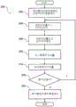
Referring now to FIG. 6, one example of a method 200 for depositing a film using ALD is shown. At 202, vacuum clamping and backside purging with reactive gases begins. At 204, a precursor dose is introduced to a reaction volume of a process chamber. At 206, the precursor dose is purged from the reaction volume after a predetermined exposure period. At 210, a plasma dose is introduced. At 214, the plasma dose is purged. At 216, one or more additional cycles may be performed. If it is determined at 216 that additional cycles are needed, control returns to 204. If 216 is false, control continues to 220 and vacuum clamping and backside purging are turned off.
Referring now to FIG. 7, timing sequences for other examples of ALD cycles are shown. LCD is line charge delay, PtB is charge to reference pressure, and PA is pump out. The LCD period is used to charge the supply lines before the actual deposition, and the PtB and PA periods are mainly used for post-deposition actions to evacuate the process chamber and reduce gas phase particles. In this example, the backside scrub is a two-level signal. A lower value is used during the soak and then a higher value is used during the remainder of the control period of the ALD cycle. Two stages may be used to allow the vacuum clamp to be turned on and the steady state vacuum pressure to be reached before the backside purge gas reaches the steady state vacuum pressure. The two-stage turn-on reduces the chance of substrate movement when the backside purge gas is turned on.
In some examples, the film is SiO2. For SiO2The film, precursor dose may include Diisopropylsilane (DIPAS), diaminosilane, N, N, N ', N' -tetraethyl (SAM24), tris [ dimethylamino ] silane]Silane (3DMAS) or other suitable precursor; the plasma gas mixture may include argon, oxygen, nitrogenGas, N2O, a combination of two or more of the above gases, or other suitable plasma gas mixture; and the back side purge gas comprises oxygen or nitrogen.
In some examples, the film is TiO2. The precursor dose may include titanium tetradimethylamide (TDMAT), titanium tetrachloride (TiCl)4) Or other suitable precursors; the plasma gas mixture may include argon, oxygen, nitrogen, N2O, a combination of two or more of the above gases, or other suitable plasma gas mixture; and the back side purge gas comprises oxygen or nitrogen.
In some examples, the film is SiN. The plasma gas mixture may include ammonia (NH)3) Nitrogen, argon, a combination of two or more of the foregoing gases, or other suitable plasma gas mixture; and the back purge gas comprises nitrogen or ammonia (NH)3)。
The foregoing description is merely illustrative in nature and is not intended to limit the present disclosure, application, or uses in any way. The broad teachings of the disclosure can be implemented in a variety of forms. Therefore, while this disclosure includes particular examples, the true scope of the disclosure should not be so limited since other modifications will become apparent upon a study of the drawings, the specification, and the following claims. As used herein, the phrase "at least one of A, B and C" should be interpreted to mean logic (a OR B OR C) using non-exclusive logic "OR" (OR) "and should not be interpreted to mean" at least one a, at least one B, and at least one C ". It should be understood that one or more steps of a method may be performed in a different order (or simultaneously) without altering the principles of the present disclosure.
In some implementations, the controller is part of a system, which may be part of the above-described embodiments. Such systems may include semiconductor processing equipment including one or more processing tools, one or more chambers, one or more platforms for performing processing, and/or specific processing components (wafer substrate supports, gas flow systems, etc.). These systems may be integrated with electronics that control operations before, during, and after processing of semiconductor wafers or substrates. An electronic device may be referred to as a "controller," which may control various components or sub-portions of a system or systems. Depending on the process requirements and/or type of system, the controller can be programmed to control any of the processes disclosed herein, including the delivery of process gases, temperature settings (e.g., heating and/or cooling), pressure settings, vacuum settings, power settings, Radio Frequency (RF) generator settings, RF matching circuit settings, frequency settings, flow settings, fluid delivery settings, position and operation settings, wafer transfer in and out of tools and other transport tools, and/or load locks connected to or interfaced with a particular system.
In general terms, a controller may be defined as an electronic device having various integrated circuits, logic, memory, and/or software to receive instructions, issue instructions, control operations, perform cleaning operations, perform endpoint measurements, and the like. Integrated circuits may include chips in the form of firmware that store program instructions, Digital Signal Processors (DSPs), chips defined as Application Specific Integrated Circuits (ASICs), and/or one or more microprocessors or microcontrollers that execute program instructions (e.g., software). The program instructions may be instructions that communicate with the controller in the form of various separate settings (or program files) that define the operating parameters for performing a particular process on or to the semiconductor wafer or to the system. In some embodiments, the operating parameters may be part of a recipe defined by a process engineer to complete one or more processing steps during the fabrication of one or more layers, materials, metals, oxides, silicon dioxide, surfaces, circuits, and/or wafer scale.
In some embodiments, the controller may be part of or coupled to a computer that is integrated into, connected to, or networked with the system, or a combination thereof. For example, the controller may be in the "cloud," or in all or a portion of the wafer host computer system, which may allow remote access for chip processing. The computer may enable the remote access system to monitor the current progress of the manufacturing operation, check a history of past manufacturing operations, check trends or performance metrics from a plurality of manufacturing operations to change parameters of the current process, set process steps after the current process, or begin a new process. In some examples, a remote computer (e.g., a server) may provide the process recipe to the system over a network, which may include a local network or the Internet. The remote computer may include a user interface that enables the entry or programming of parameters and/or settings, which are then communicated from the remote computer to the system. In some examples, the controller receives instructions in the form of data specifying parameters for each process step to be performed during one or more operations. It should be understood that the parameters may be specific to the type of process to be executed and the type of tool with which the controller is configured to interface or control. Thus, as noted above, the controllers can be distributed, such as by including one or more discrete controllers networked together and working toward a common purpose such as the processing and control described herein. An example of a distributed controller for such purposes is one or more integrated circuits within a room in communication with one or more integrated circuits located remotely (e.g., at a platform level or as part of a remote computer) that are all coupled together to control the processes of the room.
Without limitation, example systems may include a plasma etch chamber or module, a deposition chamber or module, a spin rinse chamber or module, a metal plating chamber or module, a cleaning chamber or module, a bevel edge etch chamber or module, a Physical Vapor Deposition (PVD) chamber or module, a Chemical Vapor Deposition (CVD) chamber or module, an Atomic Layer Deposition (ALD) chamber or module, an Atomic Layer Etch (ALE) chamber or module, an ion implantation chamber or module, a track chamber or module, and any other semiconductor processing system that may be associated with or used in the manufacture and/or production of semiconductor wafers.
As described above, the controller may communicate with one or more other tool circuits or modules, other tool components, cluster tools, other tool interfaces, adjacent tools, nearby tools, tools located throughout the factory, a host computer, another controller, or a tool used in material transport to and from a tool location and/or load port of a semiconductor manufacturing factory, depending on the process step or steps performed by the tool.
Claims (8)
1. A substrate processing system for depositing a film on a substrate, comprising:
a process chamber defining a reaction volume and comprising a substrate support for supporting the substrate;
a gas delivery system configured to introduce a process gas into the reaction volume of the process chamber;
a plasma generator configured to selectively generate an RF plasma within the reaction volume;
a clamping system configured to clamp the substrate to the substrate support during deposition of the film; and
a backside purge system configured to supply a reactive gas, other than an inert gas, as a purge gas to a backside edge of the substrate to purge the backside edge during deposition of the film and during generation of the RF plasma within the reaction volume,
wherein, in order to supply the purge gas,
the backside purge system is configured to flow the purge gas at a rate of 150sccm to 450sccm to purge the backside edge during generation of the RF plasma,
the backside purge system is configured to provide molecular oxygen as the purge gas, and
the backside purge system is configured to provide the molecular oxygen as the purge gas to (i) suppress at least one of plasma ignition and hollow cathode discharge characteristics near the backside edge during generation of the RF plasma within the reaction volume, and (ii) suppress parasitic power losses associated with the purge gas.
2. The substrate processing system of claim 1, wherein the clamping system comprises a vacuum clamping system to clamp the substrate to the substrate support using vacuum pressure.
3. The substrate processing system of claim 1, wherein the film comprises silicon dioxide.
4. The substrate processing system of claim 1, wherein the film is deposited using atomic layer deposition.
5. The substrate processing system of claim 2 wherein said rate is sufficient to move said substrate in the absence of said vacuum pressure.
6. The substrate processing system of claim 2, wherein the vacuum clamping system comprises:
a valve;
a chamber disposed on a substrate-facing surface of the substrate support, wherein the chamber is in fluid communication with the valve; and
a vacuum source in fluid communication with the valve.
7. The substrate processing system of claim 1, wherein the backside purge system comprises:
a valve;
a chamber disposed on a substrate-facing surface of the substrate support proximate an edge of the substrate, wherein the chamber is in fluid communication with the valve; and
a source of reactant gas in fluid communication with the valve.
8. The substrate processing system of claim 1, further comprising: a controller configured to control the gas delivery system, the plasma generator, the clamping system, and the backside purge system during one or more atomic layer deposition cycles.
Applications Claiming Priority (3)
| Application Number | Priority Date | Filing Date | Title |
|---|---|---|---|
| US14/485,142 US9460915B2 (en) | 2014-09-12 | 2014-09-12 | Systems and methods for reducing backside deposition and mitigating thickness changes at substrate edges |
| US14/485,142 | 2014-09-12 | ||
| CN201510582177.1A CN105420685B (en) | 2014-09-12 | 2015-09-14 | For the system and method for reducing backside deposition and reducing the thickness change at substrate edge |
Related Parent Applications (1)
| Application Number | Title | Priority Date | Filing Date |
|---|---|---|---|
| CN201510582177.1A Division CN105420685B (en) | 2014-09-12 | 2015-09-14 | For the system and method for reducing backside deposition and reducing the thickness change at substrate edge |
Publications (2)
| Publication Number | Publication Date |
|---|---|
| CN108642474A CN108642474A (en) | 2018-10-12 |
| CN108642474B true CN108642474B (en) | 2020-09-15 |
Family
ID=55455423
Family Applications (2)
| Application Number | Title | Priority Date | Filing Date |
|---|---|---|---|
| CN201810478814.4A Active CN108642474B (en) | 2014-09-12 | 2015-09-14 | Substrate processing system for depositing a film on a substrate |
| CN201510582177.1A Active CN105420685B (en) | 2014-09-12 | 2015-09-14 | For the system and method for reducing backside deposition and reducing the thickness change at substrate edge |
Family Applications After (1)
| Application Number | Title | Priority Date | Filing Date |
|---|---|---|---|
| CN201510582177.1A Active CN105420685B (en) | 2014-09-12 | 2015-09-14 | For the system and method for reducing backside deposition and reducing the thickness change at substrate edge |
Country Status (5)
| Country | Link |
|---|---|
| US (2) | US9460915B2 (en) |
| JP (1) | JP6578163B2 (en) |
| KR (2) | KR102454243B1 (en) |
| CN (2) | CN108642474B (en) |
| TW (2) | TWI682062B (en) |
Families Citing this family (12)
| Publication number | Priority date | Publication date | Assignee | Title |
|---|---|---|---|---|
| US11072860B2 (en) | 2014-08-22 | 2021-07-27 | Lam Research Corporation | Fill on demand ampoule refill |
| US10094018B2 (en) * | 2014-10-16 | 2018-10-09 | Lam Research Corporation | Dynamic precursor dosing for atomic layer deposition |
| TWI734770B (en) * | 2016-04-24 | 2021-08-01 | 美商應用材料股份有限公司 | Apparatus for prevention of backside deposition in a spatial ald process chamber |
| US10777386B2 (en) * | 2017-10-17 | 2020-09-15 | Lam Research Corporation | Methods for controlling plasma glow discharge in a plasma chamber |
| CN111433886A (en) * | 2017-11-29 | 2020-07-17 | 东京毅力科创株式会社 | Backside friction reduction of substrates |
| JP7178177B2 (en) * | 2018-03-22 | 2022-11-25 | 東京エレクトロン株式会社 | Substrate processing equipment |
| WO2020159708A1 (en) * | 2019-01-31 | 2020-08-06 | Lam Research Corporation | Showerhead with configurable gas outlets |
| US11031236B2 (en) | 2019-10-01 | 2021-06-08 | Taiwan Semiconductor Manufacturing Co., Ltd. | Method for improving surface of semiconductor device |
| CN112981372B (en) * | 2019-12-12 | 2024-02-13 | Asm Ip私人控股有限公司 | Substrate support plate, substrate processing apparatus including the same, and substrate processing method |
| KR20220119112A (en) * | 2019-12-20 | 2022-08-26 | 램 리써치 코포레이션 | Semiconductor processing chucks featuring recessed regions near the outer periphery of the wafer for edge/center non-uniformity mitigation |
| US11923295B2 (en) | 2020-02-19 | 2024-03-05 | Taiwan Semiconductor Manufacturing Co., Ltd. | Interconnect level with high resistance layer and method of forming the same |
| US11495483B2 (en) * | 2020-10-15 | 2022-11-08 | Applied Materials, Inc. | Backside gas leakby for bevel deposition reduction |
Citations (2)
| Publication number | Priority date | Publication date | Assignee | Title |
|---|---|---|---|---|
| US6159299A (en) * | 1999-02-09 | 2000-12-12 | Applied Materials, Inc. | Wafer pedestal with a purge ring |
| CN101147248A (en) * | 2005-03-21 | 2008-03-19 | 东京毅力科创株式会社 | Plasma enhanced atomic layer deposition system and method |
Family Cites Families (18)
| Publication number | Priority date | Publication date | Assignee | Title |
|---|---|---|---|---|
| US5871811A (en) * | 1986-12-19 | 1999-02-16 | Applied Materials, Inc. | Method for protecting against deposition on a selected region of a substrate |
| US5238499A (en) | 1990-07-16 | 1993-08-24 | Novellus Systems, Inc. | Gas-based substrate protection during processing |
| US5275976A (en) * | 1990-12-27 | 1994-01-04 | Texas Instruments Incorporated | Process chamber purge module for semiconductor processing equipment |
| US5534072A (en) * | 1992-06-24 | 1996-07-09 | Anelva Corporation | Integrated module multi-chamber CVD processing system and its method for processing subtrates |
| US5292554A (en) * | 1992-11-12 | 1994-03-08 | Applied Materials, Inc. | Deposition apparatus using a perforated pumping plate |
| US6190732B1 (en) * | 1998-09-03 | 2001-02-20 | Cvc Products, Inc. | Method and system for dispensing process gas for fabricating a device on a substrate |
| US6037258A (en) * | 1999-05-07 | 2000-03-14 | Taiwan Semiconductor Manufacturing Company | Method of forming a smooth copper seed layer for a copper damascene structure |
| US6223447B1 (en) | 2000-02-15 | 2001-05-01 | Applied Materials, Inc. | Fastening device for a purge ring |
| AU2003238853A1 (en) * | 2002-01-25 | 2003-09-02 | Applied Materials, Inc. | Apparatus for cyclical deposition of thin films |
| US7138014B2 (en) * | 2002-01-28 | 2006-11-21 | Applied Materials, Inc. | Electroless deposition apparatus |
| KR100682305B1 (en) * | 2005-05-24 | 2007-02-15 | 주식회사 에이디피엔지니어링 | Clamping apparatus |
| US7993465B2 (en) | 2006-09-07 | 2011-08-09 | Applied Materials, Inc. | Electrostatic chuck cleaning during semiconductor substrate processing |
| US20080179287A1 (en) | 2007-01-30 | 2008-07-31 | Collins Kenneth S | Process for wafer backside polymer removal with wafer front side gas purge |
| JP2008198739A (en) * | 2007-02-09 | 2008-08-28 | Tokyo Electron Ltd | Placing table structure, treating apparatus using this structure, and method for using this apparatus |
| US7699935B2 (en) * | 2008-06-19 | 2010-04-20 | Applied Materials, Inc. | Method and system for supplying a cleaning gas into a process chamber |
| WO2010016499A1 (en) * | 2008-08-05 | 2010-02-11 | 東京エレクトロン株式会社 | Placing table structure |
| GB201207448D0 (en) * | 2012-04-26 | 2012-06-13 | Spts Technologies Ltd | Method of depositing silicon dioxide films |
| CN104008997A (en) * | 2014-06-04 | 2014-08-27 | 复旦大学 | Ultra-low dielectric constant insulating film and manufacturing method thereof |
-
2014
- 2014-09-12 US US14/485,142 patent/US9460915B2/en active Active
-
2015
- 2015-09-04 JP JP2015174358A patent/JP6578163B2/en active Active
- 2015-09-08 KR KR1020150126922A patent/KR102454243B1/en active IP Right Grant
- 2015-09-10 TW TW108125499A patent/TWI682062B/en active
- 2015-09-10 TW TW104129861A patent/TWI675124B/en active
- 2015-09-14 CN CN201810478814.4A patent/CN108642474B/en active Active
- 2015-09-14 CN CN201510582177.1A patent/CN105420685B/en active Active
-
2016
- 2016-09-02 US US15/255,337 patent/US9852901B2/en active Active
-
2022
- 2022-10-07 KR KR1020220128496A patent/KR102598660B1/en active IP Right Grant
Patent Citations (2)
| Publication number | Priority date | Publication date | Assignee | Title |
|---|---|---|---|---|
| US6159299A (en) * | 1999-02-09 | 2000-12-12 | Applied Materials, Inc. | Wafer pedestal with a purge ring |
| CN101147248A (en) * | 2005-03-21 | 2008-03-19 | 东京毅力科创株式会社 | Plasma enhanced atomic layer deposition system and method |
Also Published As
| Publication number | Publication date |
|---|---|
| US20160079057A1 (en) | 2016-03-17 |
| KR102598660B1 (en) | 2023-11-06 |
| TW201623684A (en) | 2016-07-01 |
| KR20160031419A (en) | 2016-03-22 |
| TW201938839A (en) | 2019-10-01 |
| TWI682062B (en) | 2020-01-11 |
| KR102454243B1 (en) | 2022-10-12 |
| US20160372318A1 (en) | 2016-12-22 |
| KR20220142411A (en) | 2022-10-21 |
| US9460915B2 (en) | 2016-10-04 |
| CN105420685A (en) | 2016-03-23 |
| JP2016063223A (en) | 2016-04-25 |
| US9852901B2 (en) | 2017-12-26 |
| CN105420685B (en) | 2018-06-15 |
| JP6578163B2 (en) | 2019-09-18 |
| CN108642474A (en) | 2018-10-12 |
| TWI675124B (en) | 2019-10-21 |
Similar Documents
| Publication | Publication Date | Title |
|---|---|---|
| CN108642474B (en) | Substrate processing system for depositing a film on a substrate | |
| JP7232864B2 (en) | Substrate processing system for suppressing parasitic plasma to reduce within-wafer non-uniformity | |
| TWI687539B (en) | Systems and methods for decreasing carbon-hydrogen content of amorphous carbon hardmask films | |
| US9520295B2 (en) | Metal doping of amorphous carbon and silicon films used as hardmasks in substrate processing systems | |
| KR102410092B1 (en) | Atomic layer deposition of tungsten | |
| TWI805644B (en) | Systems and methods for depositing a homogenous interface for pecvd metal-doped carbon hardmasks | |
| US20220181147A1 (en) | High etch selectivity, low stress ashable carbon hard mask | |
| KR102510611B1 (en) | Method for Depositing Thick Tetraethyl Orthosilicate Films with Low Compressive Stress, High Film Stability and Low Shrinkage at High Deposition Rates | |
| US20200098562A1 (en) | Dual frequency silane-based silicon dioxide deposition to minimize film instability |
Legal Events
| Date | Code | Title | Description |
|---|---|---|---|
| PB01 | Publication | ||
| PB01 | Publication | ||
| SE01 | Entry into force of request for substantive examination | ||
| SE01 | Entry into force of request for substantive examination | ||
| GR01 | Patent grant | ||
| GR01 | Patent grant |