CN108628552B - Method for improving Flash wear life, control device and storage system - Google Patents
Method for improving Flash wear life, control device and storage system Download PDFInfo
- Publication number
- CN108628552B CN108628552B CN201810441749.8A CN201810441749A CN108628552B CN 108628552 B CN108628552 B CN 108628552B CN 201810441749 A CN201810441749 A CN 201810441749A CN 108628552 B CN108628552 B CN 108628552B
- Authority
- CN
- China
- Prior art keywords
- data
- level threshold
- flash
- rber
- cbe
- Prior art date
- Legal status (The legal status is an assumption and is not a legal conclusion. Google has not performed a legal analysis and makes no representation as to the accuracy of the status listed.)
- Active
Links
Images


Classifications
-
- G—PHYSICS
- G06—COMPUTING OR CALCULATING; COUNTING
- G06F—ELECTRIC DIGITAL DATA PROCESSING
- G06F3/00—Input arrangements for transferring data to be processed into a form capable of being handled by the computer; Output arrangements for transferring data from processing unit to output unit, e.g. interface arrangements
- G06F3/06—Digital input from, or digital output to, record carriers, e.g. RAID, emulated record carriers or networked record carriers
- G06F3/0601—Interfaces specially adapted for storage systems
- G06F3/0602—Interfaces specially adapted for storage systems specifically adapted to achieve a particular effect
- G06F3/0614—Improving the reliability of storage systems
- G06F3/0616—Improving the reliability of storage systems in relation to life time, e.g. increasing Mean Time Between Failures [MTBF]
-
- G—PHYSICS
- G06—COMPUTING OR CALCULATING; COUNTING
- G06F—ELECTRIC DIGITAL DATA PROCESSING
- G06F12/00—Accessing, addressing or allocating within memory systems or architectures
- G06F12/02—Addressing or allocation; Relocation
- G06F12/0223—User address space allocation, e.g. contiguous or non contiguous base addressing
- G06F12/023—Free address space management
- G06F12/0238—Memory management in non-volatile memory, e.g. resistive RAM or ferroelectric memory
- G06F12/0246—Memory management in non-volatile memory, e.g. resistive RAM or ferroelectric memory in block erasable memory, e.g. flash memory
-
- G—PHYSICS
- G06—COMPUTING OR CALCULATING; COUNTING
- G06F—ELECTRIC DIGITAL DATA PROCESSING
- G06F3/00—Input arrangements for transferring data to be processed into a form capable of being handled by the computer; Output arrangements for transferring data from processing unit to output unit, e.g. interface arrangements
- G06F3/06—Digital input from, or digital output to, record carriers, e.g. RAID, emulated record carriers or networked record carriers
- G06F3/0601—Interfaces specially adapted for storage systems
- G06F3/0628—Interfaces specially adapted for storage systems making use of a particular technique
- G06F3/0629—Configuration or reconfiguration of storage systems
- G06F3/0634—Configuration or reconfiguration of storage systems by changing the state or mode of one or more devices
-
- G—PHYSICS
- G06—COMPUTING OR CALCULATING; COUNTING
- G06F—ELECTRIC DIGITAL DATA PROCESSING
- G06F3/00—Input arrangements for transferring data to be processed into a form capable of being handled by the computer; Output arrangements for transferring data from processing unit to output unit, e.g. interface arrangements
- G06F3/06—Digital input from, or digital output to, record carriers, e.g. RAID, emulated record carriers or networked record carriers
- G06F3/0601—Interfaces specially adapted for storage systems
- G06F3/0628—Interfaces specially adapted for storage systems making use of a particular technique
- G06F3/0638—Organizing or formatting or addressing of data
- G06F3/064—Management of blocks
-
- G—PHYSICS
- G06—COMPUTING OR CALCULATING; COUNTING
- G06F—ELECTRIC DIGITAL DATA PROCESSING
- G06F3/00—Input arrangements for transferring data to be processed into a form capable of being handled by the computer; Output arrangements for transferring data from processing unit to output unit, e.g. interface arrangements
- G06F3/06—Digital input from, or digital output to, record carriers, e.g. RAID, emulated record carriers or networked record carriers
- G06F3/0601—Interfaces specially adapted for storage systems
- G06F3/0628—Interfaces specially adapted for storage systems making use of a particular technique
- G06F3/0646—Horizontal data movement in storage systems, i.e. moving data in between storage devices or systems
- G06F3/0647—Migration mechanisms
- G06F3/0649—Lifecycle management
-
- G—PHYSICS
- G06—COMPUTING OR CALCULATING; COUNTING
- G06F—ELECTRIC DIGITAL DATA PROCESSING
- G06F3/00—Input arrangements for transferring data to be processed into a form capable of being handled by the computer; Output arrangements for transferring data from processing unit to output unit, e.g. interface arrangements
- G06F3/06—Digital input from, or digital output to, record carriers, e.g. RAID, emulated record carriers or networked record carriers
- G06F3/0601—Interfaces specially adapted for storage systems
- G06F3/0628—Interfaces specially adapted for storage systems making use of a particular technique
- G06F3/0653—Monitoring storage devices or systems
-
- G—PHYSICS
- G06—COMPUTING OR CALCULATING; COUNTING
- G06F—ELECTRIC DIGITAL DATA PROCESSING
- G06F3/00—Input arrangements for transferring data to be processed into a form capable of being handled by the computer; Output arrangements for transferring data from processing unit to output unit, e.g. interface arrangements
- G06F3/06—Digital input from, or digital output to, record carriers, e.g. RAID, emulated record carriers or networked record carriers
- G06F3/0601—Interfaces specially adapted for storage systems
- G06F3/0628—Interfaces specially adapted for storage systems making use of a particular technique
- G06F3/0655—Vertical data movement, i.e. input-output transfer; data movement between one or more hosts and one or more storage devices
-
- G—PHYSICS
- G06—COMPUTING OR CALCULATING; COUNTING
- G06F—ELECTRIC DIGITAL DATA PROCESSING
- G06F3/00—Input arrangements for transferring data to be processed into a form capable of being handled by the computer; Output arrangements for transferring data from processing unit to output unit, e.g. interface arrangements
- G06F3/06—Digital input from, or digital output to, record carriers, e.g. RAID, emulated record carriers or networked record carriers
- G06F3/0601—Interfaces specially adapted for storage systems
- G06F3/0668—Interfaces specially adapted for storage systems adopting a particular infrastructure
- G06F3/0671—In-line storage system
- G06F3/0673—Single storage device
- G06F3/0679—Non-volatile semiconductor memory device, e.g. flash memory, one time programmable memory [OTP]
-
- G—PHYSICS
- G06—COMPUTING OR CALCULATING; COUNTING
- G06F—ELECTRIC DIGITAL DATA PROCESSING
- G06F2212/00—Indexing scheme relating to accessing, addressing or allocation within memory systems or architectures
- G06F2212/72—Details relating to flash memory management
- G06F2212/7205—Cleaning, compaction, garbage collection, erase control
Landscapes
- Engineering & Computer Science (AREA)
- Theoretical Computer Science (AREA)
- Physics & Mathematics (AREA)
- General Engineering & Computer Science (AREA)
- General Physics & Mathematics (AREA)
- Human Computer Interaction (AREA)
- Techniques For Improving Reliability Of Storages (AREA)
Abstract
The invention discloses a method for improving Flash wear life, a control device and a storage system, wherein the method comprises the following steps: collecting original error rates RBER and corrected error rates CBE of different blocks/pages on each Flash chip; when the RBER is increased to a certain degree, calculating to obtain an optimal read level threshold value of the corresponding Block/Page and writing the optimal read level threshold value into a corresponding Flash chip; and classifying the idle blocks/pages according to the CBE, allocating the blocks/pages with lower CBR to the data with high update frequency, and allocating the blocks/pages with higher CBR to the data with low update frequency. According to the method, the RBER is reduced by adjusting the read level threshold value, and the damage speed of the block can be delayed by matching the updating characteristics of the data with the duration abrasion of the Flash, so that the abrasion life of the Flash is prolonged. The invention can be applied to various fields such as solid state disk, disk array, solid state cache, distributed storage system, big data application and the like, and has wide application prospect.
Description
Technical Field
The invention belongs to the technical field of storage, relates to a method, a control device and a storage system for prolonging the wear life of NAND Flash, and particularly relates to a method, a control device and a storage system for automatically adapting to adverse effects caused by Flash wear by utilizing an original error rate and an error rate after error correction, wherein the purpose of prolonging the life of Flash is realized by adjusting a read level threshold (a feedback strategy) and updating characteristics of matched data and the Endurance wear of Flash (a feedforward strategy).
Background
NAND Flash (Flash) is a non-volatile random access storage medium based on a Floating Gate transistor design that latches charge through the Floating Gate, where it is stored, and they can still be retained without power supply. The NAND Flash chip has been widely applied in a magnetic disk system, such as a Solid State Disk (SSD), an NVM-e solid state disk, a full Flash disk array, and the like. Common Flash chips and technologies include 2D MLC NAND, 2D TLC NAND, 3D TLC NAND, and the like.
The NAND Flash chip is composed of a plurality of blocks (blocks), which are the smallest units capable of performing an erase operation, and are generally composed of a plurality of pages; page is the smallest unit capable of performing programming and reading operations, and is typically 4KB/8KB/16KB/32KB, etc. Before the NAND Flash is written in, erasing for 1 time and then writing for 1 time by the Block, which is called as 1-time PE Cycle, and the Endurance (durability) is used for measuring the reliability index of the erasing life of the NAND Flash; the reduce refers to the capability of the NAND Flash to Erase and write data repeatedly under certain test conditions, i.e. PE (Program/Erase) Cycle corresponding to the NAND Flash.
The original bit error rate RBER of NAND Flash is usually high, and an ecc (error Correcting code) error correction code needs to be adopted for error correction processing. Common error correcting codes include BCH, RS and the most widely used LDPC code in Flash controllers. Among them, low density parity check codes (LDPC) are considered as a type of codes that can achieve a Frame Error Rate (FER) approaching Shannon Limit (Shannon Limit). For this type of encoding to be applied to NAND flash, it must not only be decoded excellently but also be suitable for implementation on large scale integrated circuits (VLSI). Quasi-cyclic LDPC codes (QC-LDPC) can meet these two requirements. The H matrix of the QC-LDPC contains a cyclic matrix, so that the high-performance error correction performance is achieved, and the structure of the cyclic matrix is beneficial to VLSI implementation.
RBER (raw Bit Error rate) refers to the probability of one Bit Error occurring when ECC Error correction is not performed, and RBER is an important index for measuring NAND quality. The PE increases, the number of times of PE is worsened, and the error tendency is exponentially distributed, wherein one main reason is that erasing causes abrasion of a floating gate oxide layer, and the other main reason is that as PE increases, the threshold value of read data can drift from the initially set threshold value (Thr1, Thr2, Thr3 and the like), so that RBER is greatly increased, and finally, the error correction capability of the ECC is exceeded. As shown in fig. 1, at time t1, the state of each memory unit of Flash and the corresponding position of the read threshold correspond to the initial state, and each state maintains a good distance between the programmed (written) voltage value and the threshold value, so that the RBER is low. the time t2 shows that after a period of reading and writing, the memory cell is subjected to a certain amount of wear, and each programmed state becomes wider and is directly closer to each other, which is likely to cause errors. More seriously, the threshold thresholds between states drift. If the thresholds are not dynamically adjusted, it is obvious that a higher RBER is caused, and the service life of Flash is reduced. The drift of these threshold values not only changes with the PE value of Flash Blocks, but also is related to the quality of Blocks, even the relative position of the Flash chip, and the read-write frequency of the adjacent Blocks, and it is difficult to adapt to the whole dynamic change in a preset manner, so an adaptive feedback mechanism is required to cope with the drift.
Correct Bit Error (CBE) refers to the number of erroneous bits that an ECC Error correction code finds and corrects. When an error Bit on a certain Page or Block reaches a certain degree, ECC cannot correct, and the Page or Block cannot be used and is marked as a Block damage by the system. Usually, a solid state disk reserves a fixed number of redundant Block spaces, and when the number of damaged blocks exceeds the number of redundant blocks, the solid state disk cannot work normally. Therefore, the CBE is an important quality parameter of Flash Blocks/Pages after ECC, how to utilize the CBE to delay the Block damage Block number to reach a specified upper limit as much as possible is an important technology for prolonging the service life of the solid state disk.
NAND Flash chips typically require one or more NAND controllers to accomplish read and write control. As shown in FIG. 2, the NAND controller typically contains a CPU, RAM/ROM, Firmware to perform the control read and write processes and logic, and a bus to connect to the Flash chip population. From function division, Firmware in the NAND controller comprises a flash memory logical/physical address translation layer (FTL), Wear-leveling (Wear-leveling), Garbage Collection (Garbage Collection) and other main functional modules.
The generation of GC (garbage collection) garbage collection is mainly due to the fact that the Block of Nand Flash has an 'Erase-Before-Write' characteristic, and a remote update method is actually adopted for the Block update of a file system, namely the Block of the file system is written at the position of Nand physical Block 0 for the first time, the next update is possibly written at the position of Nand physical Block 1, and the originally written data becomes dirty data. Therefore, the main purpose of the GC is to carry out the dirty data space recovery process after the Nand Flash space is used to a certain extent, and simultaneously, to move the valid data to a new position. Therefore, it is expected that all candidate blocks of the GC can be dirty data, so that only Erase is needed for recovery, and then the recovered candidate blocks contain a very small amount of valid data by compromise, so that performance degradation caused by selection calculation of the candidate blocks and the valid data and valid data movement is reduced.
The purpose of WL (Wear-Leveling) Wear Leveling is mainly to prevent Nand some physical blocks from being frequently erased to cause poor data retention, and then to cause a large amount of Bitflips, even ECC Error or Bad blocks, to be generated, and data is therefore wrong and can not be reused, which is disastrous. The appearance of WL just solves the problems, all Block erasing and writing can be in the same level, the service life is balanced and developed, and the data security is ensured by the good idea that the best is true. There are two types of WL: dynamic WL and static WL. In brief, the dynamic WL selects the Block with the least erasing times for use each time, while the static WL moves Cold Data which is not modified for a long time from the Block with the less erasing times to the Block with the more erasing times, so that the Block with the less erasing times is reused. A general dynamic WL occurs at Write Request, while a static WL occurs at idle phase periodically checking for trigger condition execution and has the WL effect of global Block.
At present, the functional modules only use PE information of physical Blocks (Flash Blocks) and cold and hot information (write frequency is high and low) of a user data logical address (LBA), and CBE information of each physical Block/Page is ignored.
Disclosure of Invention
The purpose of the invention is as follows: aiming at the defects of the prior art, the invention aims to provide a method, a control device and a storage system for improving the Flash wear life, which utilize the original bit error rate RBER and the error code correction CBE to correct the adverse effect caused by Flash wear and realize the purpose of prolonging the Flash life by adjusting the read level threshold value, the update frequency of matched data and the Endurance wear of Flash.
The technical scheme is as follows: in order to achieve the purpose, the invention adopts the following technical scheme:
a method for improving Flash wear life mainly comprises the following two aspects:
collecting original bit error rates RBER of different blocks/pages on each Flash chip, calculating to obtain an optimal read level threshold value of the corresponding Block/Page when the RBER is increased to a certain degree, and writing the optimal read level threshold value into the corresponding Flash chip; the optimal reading level threshold is obtained by inquiring a relation table of a pre-acquired RBER and the reading level threshold, or the optimal reading level threshold is selected from a plurality of possible reading level thresholds on line according to a likelihood function;
collecting the corrected error code number CBE of different blocks/pages on each Flash chip, classifying the idle blocks/pages according to the CBE, allocating the blocks/pages with lower CBR to the data with high update frequency, and allocating the blocks/pages with higher CBR to the data with low update frequency; the high-low information of the data updating frequency is judged according to the LBA cold-hot counter of the user logical address space, or is distinguished according to the source of the data writing request.
As a preferred embodiment, the optimal read level threshold is obtained by using a table look-up method, and the relationship table between RBER and read level threshold is obtained according to the following method:
repeatedly performing read-write operation on a group of Flash test chips, and recording the value of the RBER;
when the RBER value changes to the next interval, stopping writing, only performing reading, repeatedly trying different reading level thresholds, and finding the optimal value;
continuing the read-write operation to enable the chip to be continuously worn, and calibrating an optimal read level threshold in a higher RBER interval;
and circulating the above processes until the read level thresholds corresponding to all RBER intervals are obtained.
As another preferred embodiment, an optimal read level threshold is obtained by online calculation, and the specific method for online calculation of the optimal read level threshold includes:
the historical read-out level and the corresponding stored data information of each Block in a period of time are saved;
when the read level threshold value needs to be optimized, a plurality of possible level drift values are deduced according to the current read level threshold value so as to obtain a new possible read level threshold value;
and calculating the ML function in the last time period by using the obtained plurality of new possible read level thresholds, and selecting the read level threshold corresponding to the maximum ML function as the optimal read level threshold.
As a preferred embodiment, the data write allocation is implemented by acquiring data hot and cold information according to the LBA cold and hot counter, which specifically includes:
dividing the Block/Page which can be redistributed and is generated by the garbage recycling/wear balancing module into a plurality of grades according to the CBE information;
receiving a user data writing request, and inquiring an LBA cold and hot counter of the written data to obtain the cold and hot degree of the data;
and allocating a Flash Block/Page with lower CBE for hotter data, and allocating a Flash Block/Page with higher CBE for colder data.
As another preferred embodiment, the data write allocation is implemented by distinguishing the sources of the data write requests, and specifically includes:
dividing the redistributed Block/Page generated by the garbage recovery/wear leveling module into a high-level Block and a low-level Block according to the CBE information; arranging CBE low-level and high-level Block/Page according to FIFO queues respectively;
receiving a data write request, sequentially selecting blocks/pages from a CBE low-level queue for the user write request and executing write operation, and sequentially selecting blocks/pages from a CBE high-level queue for the garbage collection/wear leveling module data migration write request and executing write operation;
the invention discloses a control device for improving the Flash abrasion life, which comprises:
the RBER/CBE collection module is used for acquiring and storing original error rates RBER and corrected error rates CBE of different blocks/pages on each Flash chip;
the read level threshold calculation module is used for calculating to obtain the optimal read level threshold of the corresponding Block/Page when the RBER of the Block/Page of the Flash chip is increased to a certain degree; the optimal reading level threshold is obtained by inquiring a relation table of a pre-acquired RBER and the reading level threshold, or the optimal reading level threshold is selected from a plurality of possible reading level thresholds on line according to a likelihood function;
the read level threshold value adjusting module is used for receiving the optimal read level threshold value obtained by calculation and writing the optimal read level threshold value into a corresponding Flash chip;
the data write allocation module is used for classifying the idle blocks/pages according to the CBE, allocating the blocks/pages with lower CBR to the data with high update frequency, and allocating the blocks/pages with higher CBR to the data with low update frequency; the high-low information of the data updating frequency is judged according to the LBA cold-hot counter of the user logical address space, or is distinguished according to the source of the data writing request.
The invention discloses a storage system on the other hand, which comprises a Flash chip, an ECC encoding and decoding module, an address conversion module, a garbage recovery module, a wear balancing module and the control device for improving the wear life of Flash.
In another aspect of the present invention, a storage system is disclosed, which includes a Flash controller, the controller includes a memory, a processor, and a program stored in the memory and executable on the processor, and when the program is loaded into the processor, the method for improving Flash wear life according to the claims is implemented.
Has the advantages that: the method and the device adopt a strategy to adjust the read level thresholds corresponding to the blocks by tracking the change of the Block/Page along with the RBER in the data writing process and when the RBER of the Block/Page has larger change, thereby reducing the RBER. Meanwhile, the Block/Page is classified according to its CBE value. Similar CBE values indicate that Block/Page have similar Endurance lifetimes. In the process of writing data, data blocks are distributed according to the Endurance grade of Block/Page, frequently updated data are written into a lower CBE Block, and infrequently updated data are written into a relatively larger CBE Block, so that the damage speed of the blocks is delayed, and the wear life of Flash is prolonged. The invention can be applied to various fields such as solid state disk, disk array, solid state cache, distributed storage system, big data application and the like, and has wide application prospect.
Drawings
Fig. 1 is a schematic diagram illustrating a principle that a read level threshold drifts in a Flash chip writing process to increase RBER.
Fig. 2 is a hardware block diagram of a conventional Flash controller.
FIG. 3 is a flow chart of a method according to an embodiment of the present invention.
FIG. 4 is a table illustrating an example of a lookup table for RBER read level threshold according to an embodiment of the present invention.
FIG. 5 is a flowchart illustrating the lookup table calibration of RBER-read level threshold according to an embodiment of the present invention.
FIG. 6 is a flowchart illustrating an embodiment of the present invention for calculating an optimal read level threshold on-line according to RBER variation.
FIG. 7 is a flowchart illustrating the CBE write allocation according to the LBA write calculator in the embodiment of the present invention.
FIG. 8 is a flow chart of the CBE write allocation based on distinguishing between user write operations and GC/WC data migration in an embodiment of the present invention.
Detailed Description
The invention is further described with reference to the following figures and specific examples.
As shown in fig. 3, the method for improving the Flash wear life based on the original bit error rate RBER and the bit error correction CBE disclosed in the embodiment of the present invention achieves the purpose of prolonging the Flash life by adjusting the read level threshold, the update frequency of the matching data, and the reduce wear of Flash. The method comprises the following steps: collecting original error rates of different pages/blocks on each Flash chip, comparing RBER with historical data, and starting an algorithm for adjusting the read level threshold of the pages/blocks when the RBER is increased to a certain degree, so that the RBER is reduced. Since the read level threshold adversely affects RBER to form a closed-loop feedback mechanism, adjusting the read level threshold by RBER is called a feedback strategy. Another aspect is: CBEs are collected for each Block/Page, free blocks/pages are classified according to the CBEs, matching is carried out according to the degree of cold and hot (data updating frequency) of data to be written, blocks/pages with lower CBRs are allocated to hot data (data with high updating frequency), and blocks/pages with higher CBRs are allocated to cold data (data with low updating frequency). Due to the fact that the frequency of hot data updating is high, the residence time is short, the blocks/pages with low CBR are easy to release again, abrasion is naturally increased relatively, abrasion of the blocks/pages with high CBR is reduced relatively, and the purpose of natural abrasion balance is achieved. Although the common Wear Level method also has the effect of Wear leveling, the Wear leveling needs to be realized through data migration, and extra performance and Wear cost are required. The data writing distribution strategy based on the CBR can realize wear balance on the premise of not introducing extra cost, and can effectively prolong the wear life of the Flash. The CBE-based data write allocation strategy is a feed-forward strategy because the Flash wear can be improved, but the CBE is not directly changed.
In the method, the read level threshold can be calculated according to different granularities of each Page, each Block or a Zone consisting of a plurality of blocks, the finer the granularity is, the higher the accuracy of the read level threshold is, but the higher the complexity of the implementation is, and a proper compromise can be selected according to the needs in practical application. In this example, Block is taken as an example. The invention provides two specific algorithms to realize the calculation of the read level threshold value adaptive to the RBER change. One method is to use a table query mode, namely, the interval of the Flash Block changing in the RBER in the life cycle is divided in advance, N intervals are provided, and each interval corresponds to a group of read level thresholds which are set originally to adapt to the change of the RBER. The query table of RBER-read level threshold is shown in fig. 4, the left column of the table indicates different RBER intervals, and the right column of the table indicates the corresponding optimal read level threshold. In order to accurately set the read level threshold, a large amount of calibration work needs to be performed in advance, that is, a certain number of Flash chips are repeatedly read and written, and the value of the RBER is continuously recorded. When the RBER value changes to another interval, the writing operation is stopped, only the reading operation is carried out, but different reading level thresholds are repeatedly tried, and the optimal value is found. And then, continuing the read-write operation to ensure that the chip is continuously worn, and calibrating the optimal read level threshold in a higher RBER interval. And circulating the above processes until the read level thresholds corresponding to all RBER intervals are obtained.
Fig. 5 details the calibration procedure for optimizing the read level threshold described above. In step 501, a group of typical Flash chips is selected, the specific number of the chips depends on the consideration of experimental equipment, time/labor input, cost and the like, and generally, the more the chips are, the more accurate the obtained optimized value is; in step 502, the test chip is repeatedly written, chip abrasion is actively generated, and then RBER is counted; in step 503, checking whether the RBER reaches the next interval needing recalibration at the moment; if not, return to 502 to continue with the write operation (wearing the chip); if so, then 504 is entered to execute the optimized read level threshold operation; in step 504, an attempt is made to gradually change the current read level threshold, such as by one delta at a time, then a number of read operations are performed to count RBERs, and finally a read level threshold corresponding to the lowest RBER is selected in step 505. In step 506, the read level threshold obtained after optimization is maintained in the lookup table, and then the process returns to 502 to continue the write operation, so that the RBER enters the next interval to be re-optimized. The method has the characteristic of simple implementation, but cannot adapt to the change of the environmental temperature and the cross influence of PE on RBER and a reading level threshold.
The invention provides a second algorithm to realize the calculation of the read level threshold of the online self-adaptive RBER change. Firstly, the historical read level and the corresponding stored data information of each Block in a period of time need to be saved; and then determines whether the Block needs to reset a new read level threshold according to the change of the RBER of the Block. When the RBER of a certain block is increased to a certain set value, starting a process of calculating an optimal read level threshold, deducing a plurality of possible level drift values according to the current read level threshold so as to obtain a new possible read level threshold, and then selecting the optimal read level threshold based on the maximum likelihood function. The specific online calculation process is shown in fig. 6. In step 601, for each Flash Block, the read level values of the Block up to the current time, t1, t2, t3, …, are saved for a past period of time, and the real storage information (subjected to ECC error correction) corresponding to these levels, such as 101101 …. This information will be used to calculate the likelihood function. In step 602, it is checked whether the RBER corresponding to the Block at the current time is large, and if so, it indicates that a read level threshold optimization process needs to be performed on the Block at this time. A specific method is given in step 603 to find the optimal threshold. And deducing a plurality of possible level drift values according to the current read level threshold value of the block, and obtaining N new possible read level threshold values in a mode of delta,2 delta, and N delta, namely, the current level is deviated by 1 to N delta to obtain N possible read level threshold values. In step 604, likelihood functions at time periods t1, t2, t3, … are calculated for the N possible read level thresholds, respectively. The likelihood function is to calculate the probability of occurrence of the observed value according to a distribution function and the observed value, in this case, the distribution function is a positive-too distribution function, the variance is fixed, and the mean value depends on the level threshold (which varies with the read level threshold) to which the actual stored information (corrected by ECC) is applied. The saved read level values are observed sample values used to calculate the likelihood function. In this step, we use N possible read level thresholds to calculate N Maximum Likelihood (ML) functions according to the positive probability of distribution. In step 605, an optimal read level threshold is set to the maximum likelihood function value among the N possibilities. The method is more reproducible, needs more computing and storage resources, and can automatically adapt to the change of the temperature and the PE value.
In the method of the present invention, the work flow of CBE write allocation can be implemented by referring to the following processes. The CBE write allocation module receives freely allocatable Flash Block/Page from the GC/WL module, firstly, the Flash Block/Page is classified according to CBE of the Block/Page, the Flash Block/Page is divided into M levels according to CBE from low to high, the low level of the CBE indicates that the Block/Page is low in abrasion degree, and conversely, the high level of the CBE indicates that the Block/Page is high in abrasion degree. The LBA of the user logical address space is divided according to the size of a preset block, and a cold-hot counter is distributed to the user data block corresponding to each LBA to record the data updating times (writing times) on the block. The LBA whose update number is high in the unit time represents hot data, and the data whose update number is low represents cold data. The data cold and hot levels are divided according to the number of updates corresponding to the LBA. When data needs to be written, CBE write allocation first queries the data update times of the data LBA, and determines the cold and hot degree of the data according to the number. According to the cold and hot degree, distributing Flash blocks/pages corresponding to the matched CBE grades, writing hotter data into the blocks/pages with lower CBE, and writing cooler data into the blocks/pages with higher CBE, thereby achieving the purpose of self-adaptive wear balance.
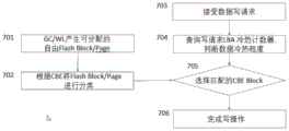
FIG. 7 shows the above process of using LBA hot and cold counters to obtain data hot and cold information and match with CBE. In step 701, a Garbage Collection (GC)/Wear Leveling (WL) module will generate re-assignable Flash blocks/pages, which will be classified into several levels according to their CBE information in step 702. A lower CBE rating indicates that the wear is minor and can be used to write frequently updated data; the residence time of the frequently updated data on the Flash/Page is short, so the Block/Page can be recovered again and the data can be written again more quickly. Conversely, a higher CBE level indicates that the wear is relatively moderate and can be used to write data with a low update frequency, and the data is indirectly protected from the Flash/Page with a higher CBE because the data is overwritten the next time. Step 703 accepts the data write request, and in step 704, queries the LBA cold-hot counter of the write data to obtain the cold-hot degree of the data. In step 705, an allocation is performed to allocate a Flash Block/Page with a lower CBE for hotter data and a Flash Block/Page with a higher CBE for cooler data. Step 706 completes the write operation. Note that step 701 and step 703 do not logically exist in a sequential order, and may be performed simultaneously.
Although the LBA counter method can reliably obtain the cooling and heating levels of the user data block, the implementation requires consumption of certain storage and computing resources. The embodiment of the invention provides another simpler realization method, which is to divide Block/Page into two types according to CBE, wherein one type is CBE low-level, and the other type is CBE high-level. The data to be written can be divided into two types according to the source of the data, wherein one type is data from a user writing request, and the other type is a request from internal data migration sent by a Flash controller GC/WL module. Internal data migration indicates that the data involved has not been updated at all over a longer period of time and may be considered cold data, and conversely, data from a user write request may be considered hot data. Thus, the workflow of CBE write allocation is simplified as: data from the user write request is assigned to the CBE low level Block/Page, while the GC/WL migration data is written to the CBE high level Block/Page.
FIG. 8 shows the above-described process of simply classifying CBEs into two categories, a high level (representing high wear) and a low level (representing low wear), and matching with user-written data and GC/WL migration data, respectively. This method does not need to rely on the LBA counter, and thus is simpler and more convenient to implement. In step 801, a Garbage Collection (GC)/Wear Leveling (WL) module will generate a re-assignable Flash Block/Page; in step 802, the above blocks/pages will be classified into two categories, high and low, according to their corresponding CBE, the distribution representing relatively heavy wear and relatively light pattern. Step 803 arranges the CBE low-level Flash Block/Page according to an FIFO queue, and step 804 arranges the CBE high-level Flash Block/Page according to the FIFO queue; step 805 accepts the data write request, distinguishes the source of the data write in step 806, queues the data write request from the user in step 807, and sorts the data migration write request from the GC/WL in step 808. In step 809, selecting blocks/pages in turn from the CBE low-level queue for the user write request and performing the write operation; in step 810, selecting blocks/pages in turn from the CBE high-level queue for the GC/WL data migration write request and performing a write operation. Note that step 801 and step 805 are not logically sequential and may be performed simultaneously.
The invention also discloses a control device for improving the Flash wear life based on the original bit error rate RBER and the corrected bit error rate CBE, which is additionally provided with the following functional modules on the basis of the original Flash controller:
the RBER/CBE collection module is used for acquiring and storing original error rates RBER and corrected error rates CBE of different blocks/pages on each Flash chip from the ECC codec; the read level threshold calculation module is used for calculating to obtain the optimal read level threshold of the corresponding Block/Page when the RBER of the Block/Page of the Flash chip is increased to a certain degree; the optimal reading level threshold is obtained by inquiring a relation table of a pre-acquired RBER and the reading level threshold, or the optimal reading level threshold is selected from a plurality of possible reading level thresholds on line according to a likelihood function; the read level threshold value adjusting module is used for receiving the optimal read level threshold value obtained by calculation and writing the optimal read level threshold value into a corresponding Flash chip; the data write allocation module is used for classifying the idle blocks/pages according to the CBE, allocating the blocks/pages with lower CBR to the data with high update frequency, and allocating the blocks/pages with higher CBR to the data with low update frequency; the high-low information of the data updating frequency is judged according to the LBA cold-hot counter of the user logical address, or is distinguished according to the source of the data writing request.
In specific implementation, the read level threshold calculation module and the data write distribution module are two software function modules which are newly added on the basis of three traditional software function modules of an FTL, a GC and a WL by a Flash controller, functions of the RBER/CBE collection module and the read level threshold adjustment module can be solidified to an independent chip or a hardware circuit, and the functions are realized through the two hardware function modules of the RBER/CBE collector and the read level threshold adjustment module. The RBER/CBE collector is responsible for collecting and storing RBER and CBE information from the ECC codec for use by the CPU. And the CPU acquires RBER information from the ECC codec, calculates a new read level threshold value and sends the new read level threshold value to the read level threshold value regulator, and the read level threshold value regulator writes the newly set read level threshold value into the Flash chip through a fixed chip IO pin.
Another embodiment of the present invention provides a storage system, which includes a Flash chip, an ECC encoding and decoding module, an address translation module, a garbage collection module, a wear leveling module, and the control device for improving the wear life of Flash.
It will be appreciated by a person skilled in the art that the modules in the above embodiments may be combined into one module or divided into sub-modules, implemented in hardware, or implemented as software modules running on a processor, or implemented in a combination thereof.
Based on the same inventive concept, another embodiment of the present invention provides a storage system, which includes a Flash controller, the controller includes a memory, a processor, and a program stored on the memory and executable on the processor, and the program realizes the method for improving the Flash wear life when being loaded into the processor.
In summary, the present invention provides an idea of using RBER and CBE information obtained after ECC error correction to perform feedback control on a read level threshold of a Flash chip, and using CBE to match cold and hot data to effectively delay a Flash wear life, and there are many methods and ways for implementing the technical solution. The components not specified in this embodiment can be implemented by the prior art.
Claims (4)
1. A method for improving Flash wear life, comprising:
collecting original bit error rates RBER of different blocks/pages on each Flash chip, calculating to obtain an optimal read level threshold value of the corresponding Block/Page when the RBER is increased to a certain degree, and writing the optimal read level threshold value into the corresponding Flash chip; the optimal reading level threshold is obtained by inquiring a relation table of a pre-acquired RBER and the reading level threshold, or the optimal reading level threshold is selected from a plurality of possible reading level thresholds on line according to a likelihood function;
collecting the corrected error code number CBE of different blocks/pages on each Flash chip, classifying the idle blocks/pages according to the CBE, allocating the blocks/pages with lower CBR to the data with high update frequency, and allocating the blocks/pages with higher CBR to the data with low update frequency; the high-low information of the data updating frequency is judged according to a LBA (logical address block addressing) cold-hot counter of a user logical address, or is distinguished according to the source of a data writing request;
obtaining an optimal read level threshold value by adopting a table look-up mode, wherein an RBER and read level threshold value relation table is obtained according to the following method:
repeatedly performing read-write operation on a group of Flash test chips, and recording the value of the RBER;
when the RBER value changes to the next interval, stopping writing, only performing reading, repeatedly trying different reading level thresholds, and finding the optimal value;
continuing the read-write operation to enable the chip to be continuously worn, and calibrating an optimal read level threshold in a higher RBER interval;
the above processes are circulated until reading level thresholds corresponding to all RBER intervals are obtained;
the optimal reading level threshold value is obtained in an online calculation mode, and the specific method for online calculating the optimal reading level threshold value comprises the following steps:
the historical read-out level and the corresponding stored data information of each Block in a period of time are saved;
when the read level threshold value needs to be optimized, a plurality of possible level drift values are deduced according to the current read level threshold value so as to obtain a new possible read level threshold value;
calculating the ML function in a first time period by using a plurality of obtained new possible read level thresholds, and selecting the read level threshold corresponding to the maximum ML function as the optimal read level threshold;
the data write distribution is realized by adopting a mode of acquiring data cold and hot information according to the LBA cold and hot counter, and the method specifically comprises the following steps:
dividing the Block/Page which can be redistributed and is generated by the garbage recycling/wear balancing module into a plurality of grades according to the CBE information;
receiving a user data writing request, and inquiring an LBA cold and hot counter of the written data to obtain the cold and hot degree of the data;
distributing Flash blocks/pages with lower CBE for hotter data, and distributing Flash blocks/pages with higher CBE for cooler data;
the data write allocation is realized by adopting a mode of distinguishing data write request sources, and the method specifically comprises the following steps:
dividing the redistributed Block/Page generated by the garbage recovery/wear leveling module into a high-level Block and a low-level Block according to the CBE information; arranging CBE low-level and high-level Block/Page according to FIFO queues respectively;
and receiving a data write request, sequentially selecting blocks/pages from the CBE low-level queue for the user write request and executing write operation, and sequentially selecting blocks/pages from the CBE high-level queue for the garbage collection/wear leveling module data migration write request and executing write operation.
2. A control device for improving Flash wear life for implementing the method for improving Flash wear life according to claim 1, characterized by comprising:
the RBER/CBE collection module is used for acquiring and storing original error rates RBER and corrected error rates CBE of different blocks/pages on each Flash chip;
the read level threshold calculation module is used for calculating to obtain the optimal read level threshold of the corresponding Block/Page when the RBER of the Block/Page of the Flash chip is increased to a certain degree; the optimal reading level threshold is obtained by inquiring a relation table of a pre-acquired RBER and the reading level threshold, or the optimal reading level threshold is selected from a plurality of possible reading level thresholds on line according to a likelihood function;
the read level threshold value adjusting module is used for receiving the optimal read level threshold value obtained by calculation and writing the optimal read level threshold value into a corresponding Flash chip;
the data write allocation module is used for classifying the idle blocks/pages according to the CBE, allocating the blocks/pages with lower CBR to the data with high update frequency, and allocating the blocks/pages with higher CBR to the data with low update frequency; the high-low information of the data updating frequency is judged according to the LBA cold-hot counter of the user logical address, or is distinguished according to the source of the data writing request.
3. A storage system comprising a Flash chip, an ECC encoding and decoding module, an address conversion module, a garbage collection module, and a wear leveling module, further comprising the control device for improving the wear life of Flash according to claim 2.
4. A storage system comprising a Flash controller, the controller comprising a memory, a processor and a program stored on the memory and executable on the processor, wherein the program when loaded into the processor implements the method for improving Flash wear life of claim 1.
Priority Applications (1)
| Application Number | Priority Date | Filing Date | Title |
|---|---|---|---|
| CN201810441749.8A CN108628552B (en) | 2018-05-10 | 2018-05-10 | Method for improving Flash wear life, control device and storage system |
Applications Claiming Priority (1)
| Application Number | Priority Date | Filing Date | Title |
|---|---|---|---|
| CN201810441749.8A CN108628552B (en) | 2018-05-10 | 2018-05-10 | Method for improving Flash wear life, control device and storage system |
Publications (2)
| Publication Number | Publication Date |
|---|---|
| CN108628552A CN108628552A (en) | 2018-10-09 |
| CN108628552B true CN108628552B (en) | 2021-02-09 |
Family
ID=63692526
Family Applications (1)
| Application Number | Title | Priority Date | Filing Date |
|---|---|---|---|
| CN201810441749.8A Active CN108628552B (en) | 2018-05-10 | 2018-05-10 | Method for improving Flash wear life, control device and storage system |
Country Status (1)
| Country | Link |
|---|---|
| CN (1) | CN108628552B (en) |
Families Citing this family (12)
| Publication number | Priority date | Publication date | Assignee | Title |
|---|---|---|---|---|
| CN111341362A (en) * | 2018-12-18 | 2020-06-26 | 深圳市中兴微电子技术有限公司 | A decoding method and device, and storage medium |
| CN109669641B (en) * | 2018-12-24 | 2022-03-29 | 深圳忆联信息系统有限公司 | Data storage method and device for reducing SSD bit error rate |
| CN109799957B (en) * | 2019-01-08 | 2022-02-18 | 郑州云海信息技术有限公司 | Mechanical hard disk service life early warning method and system based on cloud computing platform |
| CN109871594B (en) * | 2019-01-28 | 2023-02-03 | 山东华芯半导体有限公司 | NAND Flash characteristic model establishing method |
| CN110515537A (en) * | 2019-06-27 | 2019-11-29 | 鸿秦(北京)科技有限公司 | A method of extending solid-state disk service life |
| CN110471861B (en) * | 2019-07-10 | 2022-02-11 | 华为技术有限公司 | A data storage method in a flash memory device and a flash memory device |
| CN110347335B (en) * | 2019-07-30 | 2022-12-13 | 河南文正电子数据处理有限公司 | Solid state disk data storage method and device |
| CN110473583A (en) * | 2019-08-15 | 2019-11-19 | 山东华芯半导体有限公司 | A kind of operation detection method of NAND Flash |
| CN112331249B (en) * | 2020-10-15 | 2023-12-05 | 深圳安捷丽新技术有限公司 | Method, device, terminal equipment and storage medium for predicting service life of storage device |
| CN112732179B (en) * | 2020-12-29 | 2024-02-13 | 北京浪潮数据技术有限公司 | SSD data management method and related device |
| CN114942862B (en) * | 2022-04-15 | 2026-02-17 | 阿里巴巴(中国)有限公司 | Data storage method, storage server and electronic equipment |
| CN115617261A (en) * | 2022-07-14 | 2023-01-17 | 上海乐存信息科技有限公司 | An optimization method for flash wear P/E parameter selection of storage products |
Citations (2)
| Publication number | Priority date | Publication date | Assignee | Title |
|---|---|---|---|---|
| CN103092770A (en) * | 2013-01-18 | 2013-05-08 | 山东华芯半导体有限公司 | Method for reducing random access memory (RAM) expense in abrasion balanced processing |
| CN106201340A (en) * | 2016-06-29 | 2016-12-07 | 联想(北京)有限公司 | A kind of store the method for data, storage device, electronic equipment |
Family Cites Families (1)
| Publication number | Priority date | Publication date | Assignee | Title |
|---|---|---|---|---|
| US8832371B2 (en) * | 2011-04-04 | 2014-09-09 | Hitachi, Ltd. | Storage system with multiple flash memory packages and data control method therefor |
-
2018
- 2018-05-10 CN CN201810441749.8A patent/CN108628552B/en active Active
Patent Citations (2)
| Publication number | Priority date | Publication date | Assignee | Title |
|---|---|---|---|---|
| CN103092770A (en) * | 2013-01-18 | 2013-05-08 | 山东华芯半导体有限公司 | Method for reducing random access memory (RAM) expense in abrasion balanced processing |
| CN106201340A (en) * | 2016-06-29 | 2016-12-07 | 联想(北京)有限公司 | A kind of store the method for data, storage device, electronic equipment |
Also Published As
| Publication number | Publication date |
|---|---|
| CN108628552A (en) | 2018-10-09 |
Similar Documents
| Publication | Publication Date | Title |
|---|---|---|
| CN108628552B (en) | Method for improving Flash wear life, control device and storage system | |
| US11705192B2 (en) | Managing read level voltage offsets for low threshold voltage offset bin placements | |
| CN112740331B (en) | Refresh data stored at a memory component based on the memory component properties component | |
| US20220057935A1 (en) | Open block family duration limited by temperature variation | |
| US11704217B2 (en) | Charge loss scan operation management in memory devices | |
| US11693745B2 (en) | Error-handling flows in memory devices based on bins | |
| US12347511B2 (en) | Tracking charge loss in memory sub-systems | |
| US11748013B2 (en) | Grouping blocks based on power cycle and power on time | |
| US20240427500A1 (en) | Dynamic adjustment of threshold voltage offsets for wordline groups | |
| US11443830B1 (en) | Error avoidance based on voltage distribution parameters of block families | |
| US11587627B2 (en) | Determining voltage offsets for memory read operations | |
| US12572281B2 (en) | Adaptive die selection for block family scan | |
| US12482530B2 (en) | Tracking and refreshing state metrics in memory sub-systems | |
| US12417026B2 (en) | Adaptive sensing time for memory operations | |
| US11742029B2 (en) | Adjusting read-level thresholds based on write-to-write delay | |
| US11837307B2 (en) | Managing error-handling flows in memory devices | |
| US11698742B2 (en) | Garbage collection in a memory component using an adjusted parameter | |
| US11762589B2 (en) | Dynamic read-level thresholds in memory systems | |
| US20250069675A1 (en) | Enhancing read window budget using read verify | |
| US12007838B2 (en) | Accessing data using error correction operation(s) to reduce latency at a memory sub-system | |
| CN121789745A (en) | Intrinsic temperature measurement for cross temperature handling in memory devices |
Legal Events
| Date | Code | Title | Description |
|---|---|---|---|
| PB01 | Publication | ||
| PB01 | Publication | ||
| SE01 | Entry into force of request for substantive examination | ||
| SE01 | Entry into force of request for substantive examination | ||
| GR01 | Patent grant | ||
| GR01 | Patent grant |