CN108603840B - Surface enhanced Raman scattering nanofinger heating - Google Patents
Surface enhanced Raman scattering nanofinger heating Download PDFInfo
- Publication number
- CN108603840B CN108603840B CN201680079720.9A CN201680079720A CN108603840B CN 108603840 B CN108603840 B CN 108603840B CN 201680079720 A CN201680079720 A CN 201680079720A CN 108603840 B CN108603840 B CN 108603840B
- Authority
- CN
- China
- Prior art keywords
- nano
- fingers
- temperature
- sensor
- layer
- Prior art date
- Legal status (The legal status is an assumption and is not a legal conclusion. Google has not performed a legal analysis and makes no representation as to the accuracy of the status listed.)
- Active
Links
Images


Classifications
-
- G—PHYSICS
- G01—MEASURING; TESTING
- G01N—INVESTIGATING OR ANALYSING MATERIALS BY DETERMINING THEIR CHEMICAL OR PHYSICAL PROPERTIES
- G01N21/00—Investigating or analysing materials by the use of optical means, i.e. using sub-millimetre waves, infrared, visible or ultraviolet light
- G01N21/62—Systems in which the material investigated is excited whereby it emits light or causes a change in wavelength of the incident light
- G01N21/63—Systems in which the material investigated is excited whereby it emits light or causes a change in wavelength of the incident light optically excited
- G01N21/65—Raman scattering
- G01N21/658—Raman scattering enhancement Raman, e.g. surface plasmons
-
- B—PERFORMING OPERATIONS; TRANSPORTING
- B82—NANOTECHNOLOGY
- B82Y—SPECIFIC USES OR APPLICATIONS OF NANOSTRUCTURES; MEASUREMENT OR ANALYSIS OF NANOSTRUCTURES; MANUFACTURE OR TREATMENT OF NANOSTRUCTURES
- B82Y15/00—Nanotechnology for interacting, sensing or actuating, e.g. quantum dots as markers in protein assays or molecular motors
-
- B—PERFORMING OPERATIONS; TRANSPORTING
- B82—NANOTECHNOLOGY
- B82Y—SPECIFIC USES OR APPLICATIONS OF NANOSTRUCTURES; MEASUREMENT OR ANALYSIS OF NANOSTRUCTURES; MANUFACTURE OR TREATMENT OF NANOSTRUCTURES
- B82Y40/00—Manufacture or treatment of nanostructures
-
- G—PHYSICS
- G01—MEASURING; TESTING
- G01N—INVESTIGATING OR ANALYSING MATERIALS BY DETERMINING THEIR CHEMICAL OR PHYSICAL PROPERTIES
- G01N21/00—Investigating or analysing materials by the use of optical means, i.e. using sub-millimetre waves, infrared, visible or ultraviolet light
- G01N21/01—Arrangements or apparatus for facilitating the optical investigation
- G01N21/03—Cuvette constructions
- G01N21/0332—Cuvette constructions with temperature control
Abstract
A Surface Enhanced Raman Scattering (SERS) sensor may include a substrate, a conductive layer having a first portion separated from a second portion by a gap, a resistive layer in contact with and extending between the first and second portions of the conductive layer to form a resistive bridge across the gap, and a plurality of nano-fingers extending upwardly from the bridge, the resistive layer heating the nano-fingers in response to a current flowing across the bridge from the first portion to the second portion.
Description
Background
Surface Enhanced Raman Scattering (SERS) techniques may utilize nanofingers with metal tips to facilitate sensing of interactions between light illuminating an analyte carried by the nanofingers. The analyte is deposited on the nano-fingers by immersing the nano-fingers in a liquid containing the analyte and subsequently removing and evaporating the liquid. The sensed interaction can be used to identify or analyze the analyte.
Brief description of the drawings
Fig. 1 is a schematic diagram of an exemplary SERS sensor.
Fig. 2 is a schematic diagram of another exemplary SERS sensor.
Fig. 3 is a cross-sectional view of another exemplary SERS sensor.
Fig. 4 is a cross-sectional view of another exemplary SERS sensor.
Fig. 5 is a flow chart of an exemplary method of sensing with a SERS sensor.
FIG. 6 is a cross-sectional view of the sensor of FIG. 3 implementing the method of FIG. 5.
FIG. 7 is a flow chart of an exemplary method of sensing with a SERS sensor.
FIG. 8 is a cross-sectional view of the sensor of FIG. 3 implementing the method of FIG. 7.
Detailed description of the examples
The present disclosure describes a Surface Enhanced Raman Spectrometer (SERS) sensor. The disclosed SERS sensor has a structure that provides an integral resistive heater under the nano-fingers to facilitate evaporation of the analyte-containing liquid. Thus, the SERS sensor can be more easily manufactured and integrated in a complete analysis chip at low cost and with less complexity.
The present disclosure describes methods of heating a SERS sensor with a heater to facilitate bringing a nano-finger into proximity and improve sensor performance. As will be described below, heat is applied to the nano-fingers to temporarily soften the nano-fingers during use of the sensor, making the nano-fingers more susceptible to bending to facilitate their proximity for testing. By facilitating or enhancing the proximity of the nano-fingers, the sensitivity and performance of the sensor may be improved.
The present disclosure further describes methods of heating a SERS sensor with a heater to reduce or remove contaminants from the environment of the nano-fingers. As will be described further below, heat is applied to the nano-fingers and the ambient environment to temporarily heat the nano-fingers and ambient environment to degas the sensor contaminated surface prior to testing with the sensor. Because the contaminated surface may be degassed or otherwise heated to remove contaminants prior to sensing with the sensor, the nano-fingers and surrounding environment surfaces may be formed of a greater variety of materials without degrading sensor performance. The wider range of materials that can be used to form the sensor can reduce the cost and complexity of the sensor, or increase its sensitivity or performance.
Fig. 1 schematically shows an exemplary SERS sensor 20. The sensor 20 has a structure that provides an integral resistive heater under the nano-fingers to facilitate evaporation of the analyte-containing liquid. Thus, the SERS sensor can be more easily manufactured at low cost and with less complexity.
In one embodiment, resistive layer 50 is formed of a material and has a thickness to release heat at a rate of at least 10 ℃ per microsecond to heat nano-fingers 60 and the surface surrounding the environment of nano-fingers 60 to a temperature of at least 50 ℃. In one embodiment, resistive layer 50 is formed of a material and has a thickness to release heat when conducting an electrical current, thereby heating nano-fingers 60 and the surface surrounding the environment of nano-fingers 60 to a temperature above the glass transition temperature Tg of the polymer(s) of nano-fingers 60 but less than or equal to the lower of the following temperaturesTemperature of temperature: (a) a decomposition temperature of an analyte of interest on such a nano-finger 60, and (b) a detachment temperature-a temperature at which an analyte of interest leaves the surface of the nano-finger 60 or detaches from the surface of the nano-finger 60. In one embodiment, resistive layer 50 has a sheet resistance of at least 30 ohms/square and no greater than 900 ohms/square. In one embodiment, resistive layer 50 is formed of TaAl and has a thickness of 950 angstroms, and a sheet resistance of 30 ohms/square. Examples of materials from which resistive layer 50 may be formed include, but are not limited to, TaAl, WSiN, TaAiN, TiN, TaC, Ta, W, Pt, RuO2、MnOX、In2O3、SnO2ITO and ZTO, and alloys thereof.
The nano-fingers 60 comprise a two-dimensional array of structures protruding from the resistive layer 50. Each nano-finger 60 includes a bendable stem or post 68 that supports a metal ball, cap or tip 70. In one embodiment, each metal tip 70 is formed of a material that enhances SERS sensitivity, such as gold, silver, or copper. In one embodiment, each strut 68 comprises a flexible, bendable polymer. In one embodiment, each strut 68 is additionally coated with an inorganic film to inhibit the release of contaminants from the surface of the polymer strut 68.
In one embodiment, the nano-fingers 60 may be formed from acrylate monomers and have a high aspect ratio such that the length is at least two times longer than the shortest width. The nano-fingers may have an aspect ratio of 2: 1 to 20: 1 based on the longest dimension to the shortest dimension. Further, each of the nano-fingers 60 may have a width or diameter of 10nm to 1 μm. Examples of nano-fingers include antennas, struts, nanowires, rods or bars, flexible columnar or finger structures, nanoflake structures, mushroom-shaped nanostructures, pyramidal structures, and polyhedral structures (e.g., pyramids), among others.
During testing with sensor 20, a liquid or solvent containing the analyte to be tested is applied to the nano-fingers 60. In one embodiment, the nano-fingers 60 are immersed in the liquid. Subsequently, the liquid is drained or removed, leaving a liquid coating on the nano-fingers 60. Heat is applied to the nano-fingers 60 and their peripheral surfaces. In particular, a current pulse is applied to one of the portions 62, 64, wherein current is conducted across the resistive layer 50 to the other of the portions 62, 64, causing the resistive bridge formed by the layer 50 under the nano-fingers 60 to release heat. The heat given off by the resistive layer 50 accelerates the evaporation of the liquid from the nano-fingers 60 and accelerates the approaching or bending of the nano-fingers 60, bringing the tips 70 closer or into contact with each other. A laser or other light is then impinged on the analyte on the nano-fingers 60, where an interaction between the light and the analyte is sensed to identify or determine a characteristic of the analyte.
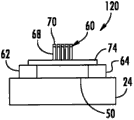
Fig. 2 schematically shows an exemplary SERS sensor 120. The sensor 120 is similar to the sensor 20 except that the sensor 120 additionally includes a passivation layer 174. Those remaining elements of sensor 120 corresponding to elements of sensor 20 are similarly numbered.
The passivation layer 174 includes a layer between the heating resistor layer 50 and the nano-fingers 60. Passivation layer 174 protects resistive layer 50 from interaction with analyte-containing liquid applied to nanofingers 60. Passivation layer 174 may additionally inhibit interactions between the liquid and resistive layer 50 that may otherwise contaminate the solution and analyte being tested. Examples of materials from which the passivation layer 174 is formed include, but are not limited to, SiN, SiC, HfOx, SiNOX、Al2O3、Ta2O5And SiOX. In one embodiment, passivation layer 174 has a thickness of at least 1000 angstroms and no greater than 8000 angstroms. The operation of sensor 120 is the same as described above with respect to sensor 20.
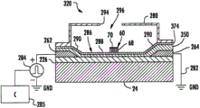
Fig. 3 is a cross-sectional view showing an exemplary SERS sensor 220. Sensor 220 includes substrate 24, interlayer dielectric 226, conductive layer 240, resistive layer 250, passivation layer 274, nano-fingers 60, housing 280, ground 282 (shown schematically), pulse voltage source 284 (shown schematically), and controller 285. The substrate 24 and the nano-fingers 60 are described above.
The interlayer dielectric 226 comprises a layer of dielectric material sandwiched between the substrate 24 and the resistive layer 250. The interlayer dielectric 226 electrically insulates the resistive layer 250 from the substrate 24. At one isIn an embodiment, interlayer dielectric 226 may comprise a material having a greater resistivity than selective resistance layer 250, such as SiO2Or TEOS. In other embodiments, the interlayer dielectric 226 may comprise other dielectric materials.
In the example shown, the portions 262, 264 are separated by a gap and cooperate with the passivation layer 274 to define and form a shape of a recess or depression 286 having a floor 288 and a side 290, wherein the passivation layer 274 follows the shape formed by the underlying selective resistive layer 250 and the underlying portions 262, 264. The bottom plate 288 supports the nano-fingers 60 rising from the bottom plate 288. Side 290 rises above floor 288. In one embodiment, the side 290 rises above the floor 288 to a height greater than the height of the nano-fingers 60. The depression 286, which is comprised of bottom plate 288 and side surfaces 294, acts as a basin to hold a solution containing the analyte in which the nano-fingers 60 are immersed.
In the example shown, the portions 262, 264 each have a sloped or inclined surface 292 defining a respective inclined sidewall 290 of the recess 288, the interior surface of which has the passivation layer 274. The angled surfaces of side 290 provide a large angle at the junction of floor 288 and side 290 to inhibit capillary retention of liquid in such corners and promote accelerated evaporation of liquid during testing. In other embodiments, the surface 292 of the portions 262, 264 may be linear, concavely curved, or stepped.
In one embodiment, the conductive portions 262, 264 of the conductive layer 240 are formed of the same material. In one embodiment, the portions 262, 264 are formed from a conductive material having a resistance of less than or equal to 0.04-0.1 ohm/square. In one embodiment, the portions 262, 264 are formed of a conductive material including, but not limited to, Al, AlCu, AlCuSi, Cu, Ti, TiN, Ta, W, Mo, Pt, and Au. In one embodiment, portions 262, 264 of layer 240 have a thickness of 4000-. In one embodiment, portions 262, 264 of layer 240 have a thickness of 950 angstroms and a sheet resistance of 425 ohms/square.
In one embodiment, the resistive layer 250 is formed of a material and has a thickness to release heat at a rate of at least 10 ℃ per microsecond to heat the nano-fingers 60 and the surface surrounding the environment of the nano-fingers 60 to a temperature above the glass transition temperature Tg of the polymer(s) of the nano-fingers 60 but less than or equal to the lower of the following temperatures: (a) a decomposition temperature of an analyte of interest on such a nano-finger 60, and (b) a detachment temperature-a temperature at which an analyte of interest leaves the surface of the nano-finger 60 or detaches from the surface of the nano-finger 60. In one embodiment, the resistive layer 250 has a sheet resistance of at least 30 ohms/square and no greater than 900 ohms/square. In one embodiment, resistive layer 250 is formed of TaAl and has a thickness of 950 angstroms, and a sheet resistance of 30 ohms/square. Examples of materials from which the resistive layer 250 may be formed include, but are not limited to, TaAl, WSiN, TaAiN, TiN, TaC, Ta, W, Pt, RuO2、MnOx、In2O3、SnO2ITO and ZTO, and alloys thereof.
The passivation layer 274 is similar to the passivation layer 74 described above, except that the passivation layer 274 overlies the underlying portions 262, 264 of the resistive layer 250 and conductive layer 240 and is shaped to form the recesses 286 described above. The passivation layer 274 protects the resistive layer 250 from interaction with analyte-containing liquid applied to the nano-fingers 60. The passivation layer 274 may additionally inhibit interaction between the liquid and the resistive layer 250Which might otherwise contaminate the solution and analyte being tested. Examples of materials from which passivation layer 274 is formed include, but are not limited to, SiN, SiC, HfOx、SiNOx、Al2O3、Ta2O5And SiOx. In one embodiment, passivation layer 274 has a thickness of at least 1000 angstroms and no greater than 8000 angstroms.
The housing 280 includes a lid, top or cover structure secured to the passivation layer 274 over the recesses 286 and over the nano-fingers 60 to form an enclosure having an interior volume for receiving and containing a liquid containing an analyte. In one embodiment, the walls of the housing 280 have a metal or metal alloy interior surface, such as a surface of nickel, gold, platinum, palladium, or rhodium or alloys thereof. In other embodiments, the walls of the housing 280 may be formed of other materials. In other embodiments, the walls of the housing 280 may alternatively be secured to other portions of the sensor 280 rather than to the passivation layer 274.
In one embodiment, the housing 280 includes a fill port 294 through which a liquid containing an analyte can be deposited into a chamber 296 formed by the housing 280. In one embodiment, the fill port is closed by a removable seal that can be peeled, punctured or torn to expose the fill port 294. In one embodiment, the fill port 294 is formed by peeling, piercing, or penetrating a portion of the wall of the housing 280. In one embodiment, portions of the shell 280 are perforated or otherwise weakened so as to be torn or peeled away to form the fill port 294 of the shell 280. In another embodiment, the housing 280 has a portion to be pierced. In yet another embodiment, the housing 280 includes a septum through which a needle may be used to deposit a liquid containing an analyte into the interior of the chamber 296.
For the purposes of this application, the term "processing unit" shall mean either currently developed or future developed computing electronics or hardware that executes sequences of instructions contained in a memory. Execution of the sequences of instructions causes the processing unit to perform steps such as generating control signals. The instructions may be loaded into a Random Access Memory (RAM) for execution by the processing unit, such as a Read Only Memory (ROM), a mass storage device, or some other persistent storage. In other embodiments, hardwired circuitry may be used in place of or in combination with software instructions to implement the functions described. For example, the controller 285 may be embodied as part of one or more Application Specific Integrated Circuits (ASICs). Unless specifically stated otherwise, the controller is not limited to any specific combination of hardware circuitry and software, nor to any particular source for the instructions executed by the processing unit.
As described above, use of sensor 220 includes applying a liquid containing an analyte to nano-fingers 60, followed by removal of such liquid. The analyte-containing liquid remaining on the nano-fingers 60 is evaporated, which causes the nano-fingers 60 to bend and come into close proximity to each other in order to sense the interaction of light with the analyte on the nano-fingers 60. To assist in the evaporation of the liquid analyte, the controller 285 outputs control signals that cause the pulse voltage source 284 to provide current pulses to the electrodes provided by the portions 262 of the conductive layer 240. Current is conducted across resistive portion 274 to portion 262 and ground 282. When a current is conducted across resistive layer 250 between portions 262 and 264, heat is generated and passes through passivation layer 274 to heat nanodiamonds 60 inside chamber 296. In one embodiment, heat is applied to heat the nano-fingers 60 and the internal cavity 296 to a temperature above the glass transition temperature Tg of the polymer material of the nano-fingers 60 but less than or equal to the lower of the following temperatures: (a) a decomposition temperature of an analyte of interest on such a nano-finger 60, and (b) a detachment temperature-a temperature at which an analyte of interest leaves the surface of the nano-finger 60 or detaches from the surface of the nano-finger 60. In other embodiments, other heating profiles may be provided by the controller 285 by application of electrical pulses by the power supply 284.
Fig. 4 is a cross-sectional view showing an exemplary SERS sensor 320. The sensor 320 is similar to the sensor 220 except that the sensor 320 includes a resistive layer 350 and a passivation layer 274 in place of the resistive layer 250 and the passivation layer 274 described above. Those elements of sensor 320 corresponding to elements of sensor 220 are similarly numbered.
The passivation layer 374 is similar to the passivation layer 274 except that the passivation layer 374 selectively covers the resistive layer 350 along the entire length and is separated from the portions 262, 264 by the resistive layer 350. In other embodiments, the passivation layer 374 may terminate before extending below the walls of the housing 280.
The use of sensor 320 is similar to the use of sensor 220 described above. A liquid containing the analyte is applied to the nano-fingers 60 and such liquid is subsequently removed. The analyte-containing liquid remaining on the nano-fingers 60 is evaporated, which causes the nano-fingers 60 to bend and come into close proximity to each other in order to sense the interaction of light with the analyte on the nano-fingers 60.
To assist in the evaporation of the liquid analyte, the controller 285 outputs control signals that cause the pulse voltage source 284 to provide current pulses to the electrodes provided by the portions 262 of the conductive layer 240. Current is conducted across resistive layer 250 to portion 262 and ground 282. When a current is conducted across resistive layer 250 between portions 262 and 264, heat is generated and passes through passivation layer 274 to heat nanodiamonds 60 inside chamber 296. In one embodiment, heat is applied to heat the nano-fingers 60 and the interior chamber 296 to a temperature above the glass transition temperature of the polymer(s) of the nano-fingers 60 but less than or equal to the lower of the following temperatures: (a) a decomposition temperature of an analyte of interest on such a nano-finger 60, and (b) a detachment temperature-a temperature at which an analyte of interest leaves the surface of the nano-finger 60 or detaches from the surface of the nano-finger 60. In other embodiments, other heating profiles may be provided by the controller 285 by application of electrical pulses by the power supply 284.
Fig. 5 and 6 show an exemplary method 400 for heating a SERS sensor using a heater to facilitate bringing a nano-finger into proximity and improve the performance of the sensor. As will be described below, heat is applied to the nano-fingers to temporarily soften the nano-fingers during use of the sensor to make them more susceptible to bending to facilitate the proximity of the nano-fingers for testing. By facilitating or enhancing the proximity of the nano-fingers, the sensitivity and performance of the sensor may be improved. Although method 400 is described and illustrated as being performed using sensor 220 (as described above), in other embodiments, method 400 may be performed using any SERS sensor described in the present disclosure or other sensors having other heaters or heating structures that may be activated to heat the SERS nano-finger.
As illustrated by block 410 and identified by stage identifier (1) in fig. 6, the nano-fingers 60 of the sensor 220 are covered with a liquid or solution 412 containing an analyte 414 to be sensed (as indicated by arrows 411). As shown in block 420 of fig. 5, the solution 412 is drained from the nano-fingers 60. In one embodiment, solution 412 is drained from chamber 296 through opening 294 or another opening (not shown), leaving residual solution 412 and analyte 414 attached to or coated on the surfaces of nano-fingers 60 and on other surfaces of chamber 296.
As indicated by block 430 in fig. 5 and identified by phase identifier (2A) in fig. 6, controller 285 outputs a control signal to cause pulse voltage source 284 to supply a current pulse to portion 262 of conductive layer 240, following instructions in a non-transitory computer readable medium. Current is conducted across resistive layer 250 to portion 262 and ground 282. When a current is conducted across resistive layer 250 between portions 262 and 264, heat (indicated by arrows 434) is generated and passes through passivation layer 274 to heat nanodiamonds 60 inside chamber 296. The heat 434 is sufficient to accelerate the evaporation of the residual solution 412 on the nano-fingers 60 (as indicated by arrows 432). Evaporation of the liquid solution may cause the nano-fingers 60 to bend or come into close proximity with each other, retaining the analyte 414 for subsequent sensing.
As further illustrated by block 430 in fig. 5 and indicated by stage identifier (2B) in fig. 6, controller 285 outputs a control signal to cause pulse voltage source 284 to supply a pulse of electrical current to portion 262 of conductive layer 240, thereby providing a sufficient amount of heat 434 to soften or make more flexible the legs 68 of nano-fingers 60. As such, the nano-fingers 60 may bend or come closer more completely or earlier in time to facilitate enhanced or faster sensing.
In one embodiment, softening the pillars 68 by heat 434 is a result of the resistive layer 250 converting electrical energy into heat so as to heat the pillars 68 to a temperature above the glass transition temperature Tg of the material(s) of the pillars 68. The amount of energy applied to soften the struts 68 may be determined by multiplying the following parameters: (a) the specific heat capacity of the material or composition of each post 68, (b) the temperature difference between the current temperature and the glass transition temperature, and (c) the amount or size of material of each post 68. In one embodiment, the controller 285 controls the application of the current pulses so as to heat the posts 68 to a temperature of at least 80 ℃. In one embodiment, each strut 68 may be formed from a polymer that can be softened. Examples of materials from which posts 68 may be formed to facilitate such softening in the event heat is applied by the heater formed by portions 262, 264 and layer 250 include, but are not limited to, polypropylene, poly-3-hydroxybutyrate, poly (vinyl acetate), polychlorotrifluoroethylene, polyamide (nylon one-6, x), polylactic acid, polyethylene terephthalate, poly (vinyl chloride), poly (vinyl alcohol), polystyrene, poly (methyl methacrylate), Acrylonitrile Butadiene Styrene (ABS), polycarbonate, epoxy (SU8), negative photoresist, and Polydimethylsiloxane (PMDS), or combinations thereof.
In one embodiment, the controller 285 causes the power source 284 to supply an electrical current that generates heat and softens the posts 68 to facilitate plastic or elastic deformation of the posts 68, thereby further facilitating the approximation of such posts 68. In one embodiment, each strut 68 softens to an extent such that each strut 68 plastically or elastically deforms, bending and moving the distance of at least one-half of the diameter of the nano-finger 60 in a direction toward and adjacent to the nano-finger 60. In one embodiment, controller 285 outputs control signals that cause power supply 284 to provide electrical pulses to portion 262 at predetermined pulse widths and amplitudes for a predetermined empirically determined amount of time, thereby softening strut 68 to a predetermined degree to promote bending.
In another embodiment, the controller 285 may adjust the duration or characteristics of the electrical pulses supplied by the power supply 284 based on sensing feedback from at least one sensor (such as optional sensor 298). For example, in one embodiment, sensor 220 may include an optical sensor 298. In other embodiments, such optical sensors may be provided by external devices, such as SERS detectors and analyzers. In such embodiments, the optical sensor senses the bending of the nano-fingers 60, wherein the controller 285 adjusts the duration or characteristics of the electrical pulse supplied by the power supply 284 according to the bending of the nano-fingers 60 sensed during the application of heat. In another embodiment, the sensor 298 may comprise a temperature sensor that senses the temperature of the interior 96, wherein the controller 285 adjusts the duration or characteristics of the electrical pulses supplied by the power supply 284 according to closed loop feedback regarding the temperature inside the chamber 296 or the sensed temperature of other portions of the sensor 220.
Fig. 7 and 8 show an exemplary method 500 of heating a SERS sensor with a heater to "pre-clean" the sensor for subsequent use. In the example shown, the method 500 applies heat to the nano-fingers 60 and the peripheral surface of the cavity 296 to reduce or remove contaminants from the environment of the nano-fingers 60. In one embodiment, heat is applied to the nano-fingers and the ambient environment to temporarily heat the nano-fingers and ambient environment, thereby degassing the sensor contaminated surface prior to testing with the sensor 220. The nano-fingers 60 and the surrounding environment surface can be formed of a greater variety of materials without degradation of the sensor due to degassing or otherwise heating the contaminated surface to remove contaminants prior to sensing with the sensor. The wider range of materials that can be used to form the sensor can reduce the cost and complexity of the sensor, or enhance its sensitivity or performance. Although method 500 is described as being performed using sensor 220 (described above), in other embodiments, method 500 may be performed using any SERS sensor described in the present disclosure or other sensors having other heaters or heating structures that may be activated to heat the SERS nano-fingers and the peripheral surface.
As illustrated in block 510 of fig. 7 and illustrated by fig. 8, a surface enhanced raman scattering sensor is provided that includes a nano-finger 60 having a polymer pillar. As shown in block 520 and by phase identifier (1) in fig. 8, prior to any sensing or prior to covering the nano-fingers 60 with the liquid solution 412, the controller 285 outputs a control signal to cause the pulse voltage source 284 to supply a pulse of current to the conductive portions 262, wherein the current is conducted across the resistive layer 250. When a current is conducted across resistive layer 250 between portions 262 and 264, heat 534 is generated and passes through passivation layer 274 to heat nanodiamge 60 inside chamber 296. In one embodiment, heat is applied to raise the nano-fingers 60 and the internal chamber 296 to a temperature sufficient to pre-clean the pillars 68 of the nano-fingers 70 and the peripheral surfaces of the chamber 296. In one embodiment, the controller 285 outputs a control signal to the pulsed voltage source 284 to inject an amount of energy to the molecules of the material of the posts 68 and the surface of the chamber 296 that approximates the enthalpy of absorption of the material(s) to facilitate degassing and "pre-cleaning" of the contaminants.
In one embodiment, the post 68 and the material comprising the interior surface of the cavity 296 are heated to a temperature (such that the enthalpy of absorption of the material(s) is reached) for a short duration of time, limited in time to inhibit significant movement of the polymer chains. Thus, contaminants can be removed from the material without altering the geometry of the nano-fingers 60.
In one embodiment, the polymer pillars 68 of the nano-fingers 60 may be formed from acrylate monomers and/or dimethyl siloxane and may have a high aspect ratio such that the length is at least two times longer than the shortest width. The nano-fingers 60 may have an aspect ratio of 2: 1 to 20: 1 based on the longest dimension to the shortest dimension. Further, each of the nano-fingers 60 may have a width or diameter of 10nm to 1 μm. Examples of nano-fingers include antennas, struts, nanowires, rods or bars, flexible columnar or finger structures, nanoflake structures, mushroom-shaped nanostructures, pyramidal structures, and polyhedral structures (e.g., pyramids), among others. In one embodiment, the polymer struts 68 may be formed from acrylate monomers, having a height of 700nm and a diameter of 70 nm. In one such embodiment, each of the nano-fingers 60 has a metal tip in the form of a 150nm diameter sphere. In one embodiment, the posts 68 and nano-fingers 60 are heated to a temperature equal to or greater than at least the detachment temperature of the anticipated or expected contaminant, and in one embodiment at or above the decomposition temperature of the anticipated contaminant.
Contaminants are expected to be those elements or particles that are expected to be present on the nano-fingers 60 due to the materials of the manufacturing environment, the sensing environment, and the SERS sensor and surrounding structures, where such elements are of a type or density to interfere with the sensing of the SERS sensor. The detachment temperatures are those temperatures at which detachment or separation of contaminants from the pillars 68 and/or the surfaces exposed to the nano-fingers 68 is expected or expected. The decomposition temperature is the temperature at which the contaminants (such as those contaminants out-gassed from the polymer comprising the posts 68 and/or exposed to the surface of the nano-fingers 68) are expected or expected to decompose.
In one embodiment, the struts 68 and the nano-fingers 60 are heated to the following temperatures: which is at or above the decomposition temperature or detachment temperature, but below the temperature at which the nano-fingers 68 deform and change shape or bend and move in a direction toward adjacent nano-fingers a distance equal to or greater than the diameter of the pillars 68 of a single nano-finger 60. In other embodiments, other heating profiles may be provided by the controller 285 by application of electrical pulses by the power supply 284.
In one embodiment, such "pre-cleaning" may be performed at the time of manufacture of the sensor 220 prior to shipment of the sensor 220. In another embodiment, such "pre-cleaning" may be performed by the end user prior to use of the sensor 220. After such "pre-cleaning", a solution 412 containing an analyte 414 may be applied to the nano-fingers 60, as indicated by the phase identifier (2), as indicated by arrow 411. After removing or draining the solution, the controller 285 may again output a control signal to cause the pulse voltage source 284 to apply a current across the resistive layer 250, again heating the nano-fingers 60 and the inner chamber 296. At this stage, heat is applied to accelerate evaporation of any residual solution 412 coating the nano-fingers 60, as indicated by arrow 432 and stage identifier (3). In one embodiment, the heat applied by resistive layer 250 is also sufficient to soften the nano-fingers 60 to further facilitate the approach of the nano-fingers 60 to a greater extent or in a shorter time, as described above with respect to method 400 and shown in fig. 6.
Although the present disclosure has been described with reference to exemplary embodiments, workers skilled in the art will recognize that changes may be made in form and detail without departing from the spirit and scope of the claimed subject matter. For example, although various exemplary embodiments have been described as including one or more features providing one or more benefits, it is contemplated that the features may be interchanged with one another or combined with one another in the exemplary embodiments or in other alternative embodiments. Because the technology of the present disclosure is relatively complex, not all variations in the technology are foreseeable. The present disclosure described with reference to the exemplary embodiments and set forth in the following claims is manifestly intended to be as broad as possible. For example, unless specifically stated otherwise, claims reciting a single particular element also encompass a plurality of such particular elements. The terms "first," "second," "third," and the like in the claims, merely distinguish between different elements and, unless otherwise specified, are not specifically related to a particular order or particular numbering of the elements in the disclosure.
Claims (11)
1. A surface enhanced raman scattering sensor comprising:
a substrate;
a conductive layer having a first portion separated from a second portion by a gap;
a resistive layer in contact with and extending between the first and second portions of the conductive layer to form a resistive bridge across the gap that heats the nano-fingers in response to current flowing from the first portion to the second portion across the resistive bridge; and
a plurality of nano-fingers extending upwardly from the resistive bridge,
a pulsed voltage source electrically connected to the first portion,
a controller to control the pulsed voltage source to supply a current across the resistive bridge to heat a region around the nano-fingers to a temperature of at least a glass transition temperature of the nano-fingers,
wherein the nano-fingers each comprise a bendable leg supporting a metal tip, the leg being formed of a material that softens in response to reaching a temperature, and wherein the controller controls the pulsed voltage source so as to heat each leg to the temperature, and the material is a polymer having a glass transition temperature.
2. The sensor of claim 1, further comprising a passivation layer between the resistive bridge and the nano-fingers.
3. The sensor of claim 1, wherein the controller controls the pulsed voltage source to pre-clean the nano-fingers by applying a current across the resistive bridge to heat the nano-fingers to a temperature above at least one of (a) a decomposition temperature and (b) a detachment temperature of a contaminant on the nano-fingers, wherein the decomposition temperature is a temperature at which the contaminant decomposes, and wherein the detachment temperature is a temperature at which the contaminant detaches or detaches from the nano-fingers.
4. The sensor of claim 1, further comprising a chamber surrounding the nano-fingers to contain a solution to be sensed, the resistive bridge being below the chamber.
5. The sensor of claim 4, wherein the resistive bridge is below a majority of the chamber.
6. The sensor of claim 1, wherein said conductive layer and said resistive layer form a recess having sides and a floor, wherein said resistive bridge forms said floor.
7. The sensor of claim 6, wherein said resistive layer forms the sides of said recess.
8. The sensor of claim 6, wherein said first and second portions form sides of said recess.
9. A method of sensing, comprising:
covering the nano-fingers of the surface enhanced raman scattering sensor of claim 1 with a solution to be sensed;
discharging the solution from the nano-fingers;
heating a region around the nano-fingers to accelerate evaporation of the residual solution, wherein the region is heated to a temperature of at least the glass transition temperature to soften the nano-fingers.
10. The method of claim 9, wherein the area around the nano-fingers is heated by applying a current across the resistive bridge under the nano-fingers and electrically connecting spaced portions of the conductive layer.
11. A precleaning method comprising:
providing a surface enhanced raman scattering sensor of claim 1;
applying an electrical pulse across a resistor below the nano-fingers to heat the nano-fingers before covering the nano-fingers with a liquid solution to be detected, wherein the nano-fingers are heated to at least one of a decomposition temperature and a detachment temperature of a contaminant on the nano-fingers, wherein the decomposition temperature is a temperature at which the contaminant decomposes, and wherein the detachment temperature is a temperature at which the contaminant detaches or separates from the nano-fingers.
Applications Claiming Priority (1)
| Application Number | Priority Date | Filing Date | Title |
|---|---|---|---|
| PCT/US2016/028478 WO2017184134A1 (en) | 2016-04-20 | 2016-04-20 | Surface enhanced raman scattering nano finger heating |
Publications (2)
| Publication Number | Publication Date |
|---|---|
| CN108603840A CN108603840A (en) | 2018-09-28 |
| CN108603840B true CN108603840B (en) | 2022-01-25 |
Family
ID=60116430
Family Applications (1)
| Application Number | Title | Priority Date | Filing Date |
|---|---|---|---|
| CN201680079720.9A Active CN108603840B (en) | 2016-04-20 | 2016-04-20 | Surface enhanced Raman scattering nanofinger heating |
Country Status (4)
| Country | Link |
|---|---|
| US (1) | US11162901B2 (en) |
| EP (1) | EP3446105B1 (en) |
| CN (1) | CN108603840B (en) |
| WO (1) | WO2017184134A1 (en) |
Families Citing this family (1)
| Publication number | Priority date | Publication date | Assignee | Title |
|---|---|---|---|---|
| US11169091B2 (en) * | 2017-07-20 | 2021-11-09 | Hewlett-Packard Development Company, L.P. | Surface enhanced luminescence analyte interrogation stage shipping and storage package |
Family Cites Families (19)
| Publication number | Priority date | Publication date | Assignee | Title |
|---|---|---|---|---|
| US6524532B1 (en) * | 1995-06-20 | 2003-02-25 | The Regents Of The University Of California | Microfabricated sleeve devices for chemical reactions |
| US7460224B2 (en) | 2005-12-19 | 2008-12-02 | Opto Trace Technologies, Inc. | Arrays of nano structures for surface-enhanced Raman scattering |
| EP2014616A3 (en) * | 2005-11-25 | 2009-04-08 | National Institute for Materials Science | Carbon nanotubes, substrate and electron emission device with such carbon nanotubes and carbon nanotube synthesizing substrate as well as methods of and apparatus for making them |
| US8582099B2 (en) * | 2005-12-19 | 2013-11-12 | Optotrace Technologies, Inc. | Monitoring network based on nano-structured sensing devices |
| US7665889B2 (en) * | 2006-05-11 | 2010-02-23 | Kevin Kjoller | Quantitative calorimetry signal for sub-micron scale thermal analysis |
| US7453565B2 (en) | 2006-06-13 | 2008-11-18 | Academia Sinica | Substrate for surface-enhanced raman spectroscopy, sers sensors, and method for preparing same |
| CN101024483B (en) | 2007-03-27 | 2010-12-29 | 吉林大学 | Constituting method for metal ordered structure surface reinforced base |
| EP2401153B1 (en) * | 2009-02-24 | 2014-04-09 | Hewlett-Packard Development Company, L.P. | Printhead and method of fabricating the same |
| CN102483354B (en) * | 2009-09-17 | 2015-12-16 | 惠普发展公司,有限责任合伙企业 | For the electrically-actuated device of surface enhanced Raman spectroscopy |
| US8993339B2 (en) * | 2011-03-23 | 2015-03-31 | Hewlett-Packard Development Company, L.P. | Hybrid nanostructures for molecular analysis |
| US9278855B2 (en) | 2011-05-27 | 2016-03-08 | Drexel University | Flexible SERS substrates with filtering capabilities |
| US9255843B2 (en) | 2011-09-26 | 2016-02-09 | University Of Maryland, College Park | Porous SERS analytical devices and methods of detecting a target analyte |
| US8994937B2 (en) | 2012-04-18 | 2015-03-31 | Hewlett-Packard Development Company, L.P. | Surface enhanced Raman spectroscopy calibration curve generating systems |
| WO2013162514A1 (en) * | 2012-04-24 | 2013-10-31 | Hewlett-Packard Development Company, L.P. | Apparatus for performing a sensing application |
| CN103077684B (en) * | 2013-01-23 | 2015-09-16 | 京东方科技集团股份有限公司 | A kind of backlight adjusting method, device and display screen |
| US10520441B2 (en) * | 2013-03-14 | 2019-12-31 | Hewlett-Packard Development Company, L.P. | Devices to detect a substance and methods of producing such a device |
| CN104568896A (en) | 2013-10-23 | 2015-04-29 | 中国科学院苏州纳米技术与纳米仿生研究所 | Surface enhanced Raman scattering sensor and preparation method thereof |
| US10712280B2 (en) * | 2016-07-22 | 2020-07-14 | Hewlett-Packard Development Company, L.P. | Heated NANO finger collapse for capture of molecules in gas for sensing |
| US11275050B2 (en) * | 2017-12-05 | 2022-03-15 | Femtodx, Inc. | Semiconductor-based biosensor and detection methods |
-
2016
- 2016-04-20 WO PCT/US2016/028478 patent/WO2017184134A1/en active Application Filing
- 2016-04-20 EP EP16899631.2A patent/EP3446105B1/en active Active
- 2016-04-20 US US16/074,298 patent/US11162901B2/en active Active
- 2016-04-20 CN CN201680079720.9A patent/CN108603840B/en active Active
Also Published As
| Publication number | Publication date |
|---|---|
| US11162901B2 (en) | 2021-11-02 |
| EP3446105A1 (en) | 2019-02-27 |
| CN108603840A (en) | 2018-09-28 |
| EP3446105A4 (en) | 2019-12-04 |
| EP3446105B1 (en) | 2021-12-08 |
| US20210190694A1 (en) | 2021-06-24 |
| WO2017184134A1 (en) | 2017-10-26 |
Similar Documents
| Publication | Publication Date | Title |
|---|---|---|
| JP6062036B2 (en) | Integrated sensor | |
| CN107110816B (en) | Digital microfluidic device with integrated electrochemical sensor | |
| US8994937B2 (en) | Surface enhanced Raman spectroscopy calibration curve generating systems | |
| US20120119315A1 (en) | Sensing devices | |
| CN108603840B (en) | Surface enhanced Raman scattering nanofinger heating | |
| JP2015505610A (en) | Molecular detector | |
| JP4967554B2 (en) | Cell capture device and temperature control method for cell capture device | |
| FR2967148A1 (en) | CONTROLLED EVAPORATION METHOD OF A LIQUID DROP IN A MICROFLUIDIC DEVICE | |
| US10712280B2 (en) | Heated NANO finger collapse for capture of molecules in gas for sensing | |
| Ghanim et al. | Design of disposable DNA biosensor microchip with amperometric detection featuring PCB substrate | |
| US9823215B2 (en) | Electrochemical sensor | |
| CN215506822U (en) | Portable array micro-fluidic chip system | |
| CN107210319B (en) | Large-scale low-cost nano sensor, nano needle and nano pump array | |
| US11583861B2 (en) | Microfluidic devices | |
| CN106158743A (en) | Utilize the manufacture method of the sensor of many inducing pixels detection multiple gases | |
| TW200912314A (en) | Biosensor and ultrasonic method of making a biosensor | |
| US9778375B2 (en) | X-ray detector and method for its production | |
| JP2005010018A (en) | Member and device for electromagnetic induction heating | |
| JP6550694B2 (en) | Extracellular potential measuring device and extracellular potential measuring method | |
| KR101366391B1 (en) | Chip for counting cells | |
| Shwetha | Design And fabrication of platinum-based mems microheater with integrated temperature sensor for the thermal analysis of greenhouse gases | |
| EP3317670B1 (en) | Gold sensor | |
| EP3344963B1 (en) | Analyte detection package with tunable lens | |
| US20180236765A1 (en) | Fluid device | |
| CN108700464B (en) | Focus adjustment for analyte detection packages |
Legal Events
| Date | Code | Title | Description |
|---|---|---|---|
| PB01 | Publication | ||
| PB01 | Publication | ||
| SE01 | Entry into force of request for substantive examination | ||
| SE01 | Entry into force of request for substantive examination | ||
| GR01 | Patent grant | ||
| GR01 | Patent grant |