CN108351820B - Protecting ECC locations when transferring correction data across a memory link - Google Patents
Protecting ECC locations when transferring correction data across a memory link Download PDFInfo
- Publication number
- CN108351820B CN108351820B CN201680067395.4A CN201680067395A CN108351820B CN 108351820 B CN108351820 B CN 108351820B CN 201680067395 A CN201680067395 A CN 201680067395A CN 108351820 B CN108351820 B CN 108351820B
- Authority
- CN
- China
- Prior art keywords
- data
- mask
- ecc
- parity bits
- error correction
- Prior art date
- Legal status (The legal status is an assumption and is not a legal conclusion. Google has not performed a legal analysis and makes no representation as to the accuracy of the status listed.)
- Active
Links
Images


Classifications
-
- G—PHYSICS
- G06—COMPUTING; CALCULATING OR COUNTING
- G06F—ELECTRIC DIGITAL DATA PROCESSING
- G06F11/00—Error detection; Error correction; Monitoring
- G06F11/07—Responding to the occurrence of a fault, e.g. fault tolerance
- G06F11/08—Error detection or correction by redundancy in data representation, e.g. by using checking codes
- G06F11/10—Adding special bits or symbols to the coded information, e.g. parity check, casting out 9's or 11's
- G06F11/1008—Adding special bits or symbols to the coded information, e.g. parity check, casting out 9's or 11's in individual solid state devices
- G06F11/1068—Adding special bits or symbols to the coded information, e.g. parity check, casting out 9's or 11's in individual solid state devices in sector programmable memories, e.g. flash disk
-
- G—PHYSICS
- G06—COMPUTING; CALCULATING OR COUNTING
- G06F—ELECTRIC DIGITAL DATA PROCESSING
- G06F11/00—Error detection; Error correction; Monitoring
- G06F11/07—Responding to the occurrence of a fault, e.g. fault tolerance
- G06F11/08—Error detection or correction by redundancy in data representation, e.g. by using checking codes
- G06F11/10—Adding special bits or symbols to the coded information, e.g. parity check, casting out 9's or 11's
- G06F11/1008—Adding special bits or symbols to the coded information, e.g. parity check, casting out 9's or 11's in individual solid state devices
- G06F11/1048—Adding special bits or symbols to the coded information, e.g. parity check, casting out 9's or 11's in individual solid state devices using arrangements adapted for a specific error detection or correction feature
-
- G—PHYSICS
- G06—COMPUTING; CALCULATING OR COUNTING
- G06F—ELECTRIC DIGITAL DATA PROCESSING
- G06F3/00—Input arrangements for transferring data to be processed into a form capable of being handled by the computer; Output arrangements for transferring data from processing unit to output unit, e.g. interface arrangements
- G06F3/06—Digital input from, or digital output to, record carriers, e.g. RAID, emulated record carriers or networked record carriers
- G06F3/0601—Interfaces specially adapted for storage systems
- G06F3/0602—Interfaces specially adapted for storage systems specifically adapted to achieve a particular effect
- G06F3/0614—Improving the reliability of storage systems
- G06F3/0619—Improving the reliability of storage systems in relation to data integrity, e.g. data losses, bit errors
-
- G—PHYSICS
- G06—COMPUTING; CALCULATING OR COUNTING
- G06F—ELECTRIC DIGITAL DATA PROCESSING
- G06F3/00—Input arrangements for transferring data to be processed into a form capable of being handled by the computer; Output arrangements for transferring data from processing unit to output unit, e.g. interface arrangements
- G06F3/06—Digital input from, or digital output to, record carriers, e.g. RAID, emulated record carriers or networked record carriers
- G06F3/0601—Interfaces specially adapted for storage systems
- G06F3/0628—Interfaces specially adapted for storage systems making use of a particular technique
- G06F3/0638—Organizing or formatting or addressing of data
- G06F3/064—Management of blocks
-
- G—PHYSICS
- G06—COMPUTING; CALCULATING OR COUNTING
- G06F—ELECTRIC DIGITAL DATA PROCESSING
- G06F3/00—Input arrangements for transferring data to be processed into a form capable of being handled by the computer; Output arrangements for transferring data from processing unit to output unit, e.g. interface arrangements
- G06F3/06—Digital input from, or digital output to, record carriers, e.g. RAID, emulated record carriers or networked record carriers
- G06F3/0601—Interfaces specially adapted for storage systems
- G06F3/0628—Interfaces specially adapted for storage systems making use of a particular technique
- G06F3/0655—Vertical data movement, i.e. input-output transfer; data movement between one or more hosts and one or more storage devices
- G06F3/0659—Command handling arrangements, e.g. command buffers, queues, command scheduling
-
- G—PHYSICS
- G06—COMPUTING; CALCULATING OR COUNTING
- G06F—ELECTRIC DIGITAL DATA PROCESSING
- G06F3/00—Input arrangements for transferring data to be processed into a form capable of being handled by the computer; Output arrangements for transferring data from processing unit to output unit, e.g. interface arrangements
- G06F3/06—Digital input from, or digital output to, record carriers, e.g. RAID, emulated record carriers or networked record carriers
- G06F3/0601—Interfaces specially adapted for storage systems
- G06F3/0668—Interfaces specially adapted for storage systems adopting a particular infrastructure
- G06F3/0671—In-line storage system
- G06F3/0673—Single storage device
- G06F3/0679—Non-volatile semiconductor memory device, e.g. flash memory, one time programmable memory [OTP]
-
- G—PHYSICS
- G11—INFORMATION STORAGE
- G11C—STATIC STORES
- G11C29/00—Checking stores for correct operation ; Subsequent repair; Testing stores during standby or offline operation
- G11C29/52—Protection of memory contents; Detection of errors in memory contents
Abstract
The memory subsystem may include a memory controller having Error Correction Code (ECC) encoder/decoder logic. The memory controller may be configured to embed link ECC parity bits in unused data mask bits and/or mask write data during a mask write operation. The memory controller may also be configured to protect at least the location of the link ECC parity bits during the mask write operation.
Description
Cross Reference to Related Applications
The benefit of U.S. provisional patent application No.62/258,155 entitled "protection AN ECC LOCATION WHEN TRANSMITTING CORRECTION DATA access a MEMORY LINK" filed on 11/20/2015 as required by 35u.s.c. 119(e), the disclosure of which is expressly incorporated herein by reference in its entirety.
Background
FIELD
The present disclosure relates generally to Integrated Circuits (ICs). More particularly, one aspect of the present disclosure relates to protecting Error Correction Code (ECC) locations when transmitting correction data across a memory link in a low power memory subsystem.
Background
Semiconductor memory devices include, for example, Static Random Access Memory (SRAM) and Dynamic Random Access Memory (DRAM). DRAM memory cells generally include one transistor and one capacitor, which enables high integration. The capacitor can be charged or discharged to store information as a corresponding bit value (e.g., '0' or '1'). Because the capacitor leaks charge, the stored information eventually fades out unless the capacitor charge is refreshed. Thus, a periodic refresh occurs. Due to refresh requirements, DRAM is referred to as dynamic memory, as opposed to SRAM and other static memory. The constant refresh of DRAM generally limits its use to computer main memory.
DRAM scaling continues to increase the total number of bits per DRAM chip. Unfortunately, DRAM scaling increases the number of weak retention cells (e.g., cells with reduced retention time). Such cells involve additional refresh cycles to maintain the stored information. Advanced DRAM processes may suffer from additional random bit refresh errors within the memory cell array due to additional refresh cycles or other process variations.
Some low power memories implement Error Correction Codes (ECC) to improve memory yield and reliability by applying ECC to any random bit errors in the memory cell array. However, ECC decoding and error correction degrade memory performance due to increased read access time. In addition, the memory link (e.g., interface) is not ECC protected and overall memory reliability is insufficient to meet high reliability and high performance system memory requirements.
SUMMARY
A method of link error correction and protection in a low power memory subsystem may include: link Error Correction Code (ECC) parity bits are embedded in unused data mask bits and/or mask write data during a mask write operation. The method may also include protecting at least the location of the link ECC parity bits during the mask write operation.
A memory subsystem may include a memory controller having Error Correction Code (ECC) encoder/decoder logic. The memory controller may be configured to embed link ECC parity bits in unused data mask bits and/or mask write data during a mask write operation. The memory controller may also be configured to protect at least the location of the link ECC parity bits during the mask write operation.
A memory subsystem may include a memory controller having Error Correction Code (ECC) encoder/decoder logic. The ECC encoder/decoder logic may be configured to embed link ECC parity bits in unused data mask bits and/or mask write data during a mask write operation. The encoder/decoder logic may be further configured to protect at least the location of the link ECC parity bits during a mask write operation. The memory subsystem may also include a memory device coupled to the memory controller via a data bus. The memory device may include a link ECC decoder and correction logic in a write path. The link ECC decoder may be configured to detect and correct link errors during a write data transfer on the data bus. The memory device may include memory ECC encoder logic in a write path. The memory ECC encoder logic may be configured to memory protect write data according to the memory ECC parity bits during storage within the memory array.
The memory subsystem may include means for embedding link Error Correction Code (ECC) parity bits in unused data mask bits and/or mask write data during a mask write operation. The low power memory subsystem may also include means for protecting at least the location of the link ECC parity bits during the mask write operation.
This has outlined rather broadly the features and technical advantages of the present disclosure in order that the detailed description that follows may be better understood. Additional features and advantages of the disclosure will be described hereinafter. It should be appreciated by those skilled in the art that the present disclosure may be readily utilized as a basis for modifying or designing other structures for carrying out the same purposes of the present disclosure. It should also be realized by those skilled in the art that such equivalent constructions do not depart from the teachings of the disclosure as set forth in the appended claims. The novel features which are believed to be characteristic of the disclosure, both as to its organization and method of operation, together with further objects and advantages will be better understood from the following description when considered in connection with the accompanying figures. It is to be expressly understood, however, that each of the figures is provided for the purpose of illustration and description only and is not intended as a definition of the limits of the present disclosure.
Brief Description of Drawings
For a more complete understanding of this disclosure, reference is now made to the following descriptions taken in conjunction with the accompanying drawing.
Fig. 1 shows a top view illustrating a low power memory subsystem of a host system-on-chip (SoC) communicatively coupled to a low power memory device, according to aspects of the present disclosure.
Fig. 2A and 2B are timing diagrams illustrating error correction code parity bit communication during a normal write command according to aspects of the present disclosure.
Fig. 3A-3C are timing diagrams illustrating various options for transferring link Error Correction Code (ECC) parity bits between a host system-on-chip (SoC) and a low power memory device during a Mask Write (MWT) command, according to aspects of the present disclosure.
Fig. 4 is a timing diagram illustrating Error Correction Code (ECC) parity bit communication within a bus during a Read (RD) command, according to aspects of the present disclosure.
Fig. 5A and 5B are diagrams illustrating corruption of link Error Correction Code (ECC) parity bits passed between a host system-on-chip (SoC) and a low power memory device during a Mask Write (MWT) command, according to aspects of the present disclosure.
Fig. 6A and 6B are diagrams illustrating protection of link Error Correction Code (ECC) parity bits passed between a host system-on-chip (SoC) and a low power memory device during a Mask Write (MWT) command, according to aspects of the present disclosure.
Fig. 7A is a diagram illustrating position protection of link Error Correction Code (ECC) parity bits passed between a host system-on-chip (SoC) and a low power memory device during a Mask Write (MWT) command, according to aspects of the present disclosure.
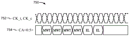
Fig. 7B illustrates a timing diagram conveying link Error Correction Code (ECC) parity bit protection information or ECC location information during a mask write command, according to aspects of the present disclosure.
Fig. 8A and 8B are flow diagrams illustrating a method for Error Correction Code (ECC) parity bit communication and position protection during a Mask Write (MWT) command, a normal write command, and a Read (RD) command, according to aspects of the present disclosure.
Fig. 9 is a block diagram illustrating a wireless communication system in which configurations of the present disclosure may be advantageously employed.
Detailed Description
The detailed description set forth below in connection with the appended drawings is intended as a description of various configurations and is not intended to represent the only configurations in which the concepts described herein may be practiced. The detailed description includes specific details in order to provide a thorough understanding of the various concepts. It will be apparent, however, to one skilled in the art that these concepts may be practiced without these specific details. In some instances, well-known structures and components are shown in block diagram form in order to avoid obscuring such concepts. As used herein, the use of the term "and/or" is intended to mean "facultative or" and the use of the term "or" is intended to mean "exclusive or".
Semiconductor memory devices include, for example, Static Random Access Memory (SRAM) and Dynamic Random Access Memory (DRAM). DRAM memory cells generally include one transistor and one capacitor, which enables high integration. The capacitor can be charged or discharged to store information as a corresponding bit value (e.g., '0' or '1'). Because the capacitor leaks charge, the stored information eventually fades away and the capacitor charge is periodically refreshed. Due to refresh requirements, DRAM is referred to as dynamic memory, as opposed to SRAM and other static memory. The constant refresh of DRAM generally limits DRAM to use as computer main memory.
DRAM scaling continues to increase the total number of bits per DRAM chip. Unfortunately, DRAM scaling increases the number of weak retention cells (e.g., cells with reduced retention time). Such cells involve additional refresh cycles to maintain the stored information. Advanced DRAM processes may suffer from additional random bit refresh errors within the memory cell array due to additional refresh cycles or other process variations. Some low power memories implement Error Correction Codes (ECC) to improve memory yield and reliability by applying ECC to any random bit errors in the memory cell array.
For example, servers and computing systems may use wide (e.g., 72-bit output/output (IO) width) memory modules to enhance the reliability of memory links and memory cell arrays. Because memory failures within a server computing system are intolerable, the reliability of the memory link is enhanced by applying ECC to memory operations. However, the storage of ECC involves additional equipment. For example, in a 72-bit IO width memory module, 8-bit ECC is assigned to each 64-bit data block of eight memory devices. Assigning 8-bit ECCs to each 64-bit data block provides protection against bit errors in both the memory interface and the memory cell array.
However, in a 72-bit IO width memory module, a ninth 64-bit (ECC) memory device is used to store eight 8-bit ECCs assigned to each 64-bit data block of the eight memory devices. Unfortunately, this memory configuration increases memory system cost and memory power. In particular, such memory configurations involve additional Printed Circuit Board (PCB) area due to the ECC memory device and the cost of supporting wider memory channels. ECC memory devices also involve standby and active power, which increases the cost associated with such memory configurations.
One technique for protecting both the memory array and the link includes transferring ECC bits between a host (e.g., a system on a chip (SoC)) and the low power memory. ECC bits may be delivered by extending the data burst length (e.g., extending a 16-bit burst length to an 18-bit burst length). Unfortunately, the extended burst length results in significant memory performance loss by reducing the net memory bandwidth. Some low power memories implement ECC to improve memory yield and reliability by applying ECC to any random bit errors in the memory cell array. However, ECC decoding and error correction within a memory device degrades memory performance due to increased read access time. Furthermore, the memory link (e.g., interface) is not ECC protected and overall memory reliability is insufficient to meet high reliability and high performance system memory specifications.
Aspects of the present disclosure relate to a memory subsystem including a host system on a chip (SoC) and a plurality of memory devices. The memory controller includes Error Correction Code (ECC) encoding and decoding blocks to generate link ECC bits for protecting write data against memory link errors and correcting any data failures caused by the memory link. The memory devices each have an array of cells for data and an ECC array for memory ECC parity bits to correct any random bit errors caused by the memory array of the memory device. These memory ECC parity bits are generated based on a memory device manufacturer's proprietary methodology that is different from the non-proprietary methodology used by the host SoC to generate the link ECC parity bits.
In aspects of the present disclosure, link ECC parity bits are generated to protect write data against link errors during transmission over a memory link (e.g., a data bus), and memory ECC parity bits are generated to protect write data within a memory device against random bit errors within a memory cell array of the memory device. In certain aspects of the present disclosure, link ECC parity bits may be transferred between the host and the memory device through a data mask pin or a data byte associated with a Mask Write (MWT) command. In the case of a mask write operation, the memory device restores the link ECC parity bits associated with the first asserted Data Mask (DM) bit (e.g., "H"), where the mask write command bit field indicates DM activity for an "m" bit data pattern. In the case of a normal write operation, the memory device recovers the link ECC bits from the DM data stream.
Aspects of the present disclosure describe techniques in which link ECC parity bits are transferred over a Data (DQ) pin or a Data Mask (DM) pin during a masked write operation. Unfortunately, when a bit error occurs on the DM bit marking the link ECC parity bit, the bit error causes the erroneous column to be decoded and the link ECC parity bit to fail. In aspects of the present disclosure, the masked write operation is extended to protect the write data using the link ECC parity bits, and also to protect the location of the link ECC parity bits. In normal write operations, the location of the link ECC data is always known and predictable. In a read operation, the memory controller may recover the memory/link ECC parity bits within the DM data stream from the memory device.
However, in a masked write operation, the location of the link ECC parity bits varies based on the number of masked bytes. In one aspect of the disclosure, information about the location of the link ECC parity bits may be protected or separately transmitted on the lower speed lines. In this aspect of the disclosure, a mask write command is followed by Data Mask (DM) ECC parity bits to protect the DM pin in a write data burst. In another aspect of the disclosure, the location of the ECC parity bits is transmitted using a mask write command to indicate the location where the link ECC parity bits are embedded in the write data burst.
Fig. 1 shows a top view of a low power memory subsystem illustrating a host system on a chip (SoC)100 coupled to a memory device 140(140-1, …, 140-N), according to aspects of the present disclosure. This aspect of the disclosure applies link Error Correction Code (ECC) parity bits to a low power memory subsystem in a mobile or computing system to protect a memory link (e.g., a data bus) from random bit errors during transmission over the memory link. More specifically, aspects of the present disclosure may complement the next generation low power Double Data Rate (DDR) specification and memory controller implementation in mobile or computing system chipsets, where the memory device uses proprietary memory ECC parity bits to protect the memory cell array from random bit errors.
Typically, host SoC100 includes various processing units that support multi-threaded operation. For the configuration shown in fig. 1, host SoC100 includes a Digital Signal Processor (DSP)102, a Graphics Processor Unit (GPU) and multimedia engine 104, a multi-core Central Processing Unit (CPU)106, a system bus 108, a memory controller 110, and a memory physical layer (PHY) 130. The DSPs 102, GPUs and multimedia engines 104, and the multi-core CPU 106 support various functions such as video, audio, graphics, gaming, and the like. Each processor core of the multi-core CPU 106 may be a Reduced Instruction Set Computing (RISC) machine, a microprocessor, or some other type of processor.
In this aspect of the disclosure, host SoC100 is communicatively coupled to memory device 140 (e.g., a low power Dynamic Random Access Memory (DRAM)) through memory PHY 130. In this configuration, memory controller 110 includes link Error Correction Code (ECC) encoder/decoder logic 120 to generate ECC parity bits 124 for data 122 (e.g., read/write data), which data 122 is communicated to one of memory devices 140 by memory PHY 130 along data bus 132(132-1, …, 132-N) and command/address bus 134(134-1, …, 134-N), which may be collectively referred to as a memory link. The link ECC parity bits 124 generated by the ECC encoder/decoder logic 120 enable the correction of any data failure caused by the memory link (e.g., the data bus 132) at the memory device 140.
As the host SoC100 increases the memory link serial data rate from, for example, three thousand two hundred (3200) megabits per second (Mbps) to six thousand four hundred (6400) Mbps, protection against memory link errors becomes more of a concern. In this configuration, the link ECC parity bits 124 ("n" bit ECC) are generated by the memory controller 110 to protect the data 122 (e.g., "m" bit write) from random bit errors during transmission on the data bus 132. Because both the link ECC parity bits 124 and the data 122 are transferred between the host SoC100 and the memory device 140 during write and read operations, any memory link errors may be detected and corrected using the link ECC parity bits 124. Furthermore, any random bit errors during transmission from the memory cell array 150 can be corrected in the ECC encoder/decoder logic 120 of the memory controller 110.
In this configuration, memory device 140 includes an array 150 of memory cells (e.g., a memory bank) for storing data 122 and an ECC array 152 for storing memory ECC parity bits 154. In this aspect of the disclosure, the memory device 140 includes memory ECC encoder logic 170 configured to generate memory ECC parity bits 172 to enable detection and correction of any random bit errors caused by the memory cell array 150 of the memory device 140 during storage of the data 122. Data 122 is stored in one of the memory cell arrays 150 (e.g., memory banks) and memory ECC parity bits 172 are stored in ECC array 152. Furthermore, any random bit errors in the memory cell array 150 may be corrected in the memory ECC decoder and correction logic 180 of the memory device 140 based on a proprietary algorithm of the memory device manufacturer that is different from the non-proprietary algorithm of the host SoC100 used to generate the link ECC parity bits 124.
The link ECC parity bits 124 from the memory controller 110 may be received by the memory device 140 through the data mask pin for the data byte associated with the mask write command. The location of the ECC bits (EL) information may be used to communicate the location of the link ECC parity bits 124 to the memory device 140. This process is performed during a Mask Write (MWT) operation, where the memory device 140 recovers the link ECC parity bits 124 from the data 122 when the first Data Mask (DM) bit is asserted (e.g., "H") and the MWT command bit field indicates DM is active. During a normal write operation, the memory device 140 may recover the link ECC parity bits 124 from the DM data stream.
In this configuration, memory device 140 includes an input/output (I/O) block 146 communicatively coupled to data bus 132 and command/address bus 134. In operation, the link ECC parity bits 124 generated by the memory controller 110 according to the non-proprietary methodology of the host SoC100 may be used by the link ECC decoder and correction logic 160 of the memory device 140 to detect and correct link errors within the data 122. In this aspect of the disclosure, the memory device 140 includes memory ECC encoder logic 170 configured to generate memory ECC parity bits 172 to enable detection and correction of any random bit errors during storage of the data 122. Accordingly, once the data 122 is corrected and/or verified, memory ECC parity bits 172 are generated within the memory ECC encoder logic 170 along the write path 142 of the memory device 140 to protect the data 122 from random bit errors during storage.
In operation, data 122 is stored in one of the memory cell arrays 150 (e.g., memory banks) and memory ECC parity bits 172 are stored in the ECC array 152. In this configuration, any random bit errors in the memory cell array 150 may be corrected in the memory ECC decoder and correction logic 180 of the memory device 140 based on the memory device manufacturer's proprietary algorithm using the memory ECC parity bits 172 stored within the UCC array 152. Accordingly, once the data 122 is corrected and/or verified, the link ECC parity bits 124 are generated within the link ECC encoder logic 190 along the read path 144 of the memory device 140 to protect the data 122 from random bit errors during transmission over the data bus 132.
In this aspect of the disclosure, host SoC100 is able to use link ECC parity bits 124 to detect and correct any memory link errors that may result from an increased memory link serial data rate (e.g., from 3200Mbps to 6400 Mbps). Additionally, any random bit errors in the memory cell array 150 may be corrected by the memory ECC decoder and correction logic 180 of the memory device 140 using the memory ECC parity bits 172. The use of the memory ECC decoder and correction logic 180 and the link ECC encoder logic 190 along the read path 144 of the memory device 140 may result in undesirable read latencies. Alternatively, the functionality of the memory ECC decoder and correction logic 180 and/or the link ECC encoder logic 190 is incorporated into the memory controller to reduce read latency.
In the memory device 140 shown in FIG. 1, an entire memory row (e.g., a 256-bit word) is typically read from the memory array during a write operation. During a mask write operation, memory ECC encoder logic 170 performs a read-modify-write operation within one of memory cell arrays 150 to perform ECC encoding using read and write data (corresponding data bytes in one of memory cell arrays 150 are used in place of masked data bytes). That is, the mask write operation enables the selected byte in the memory line to be updated so that the masked data byte is not written to the memory cell array 150. In operation, additional pins (e.g., data mask bits) are sent along with the data 122 to remove the specified write data and to restrict read-modify-write operations by specifying the write data bytes that are ignored.
Fig. 2A is a timing diagram 200 illustrating a Mask Write (MWT) command for, for example, a 128-bit write data burst 210 with an associated 16-bit data mask, where the burst length is equal to 16. In timing diagram 200, "D" refers to write data, and "M" refers to data mask bits, where each DQ byte is assigned one data mask bit. In this example, the M2 bit associated with the write data D <16:23> in the DM0 pin is asserted (e.g., "high" or "H"). As a result, mask write data 220 (e.g., write data D <16:23) is not written to the target memory cell array in memory cell array 150 (fig. 1). In response to the mask write command, a target one of the memory devices 140 performs a read operation from one of the memory cell arrays 150 and replaces the mask write data 220 with read data Q <16:23> to form write data (e.g., 128-bit write data) for memory ECC encoding using the memory ECC encoder logic 170. Memory ECC encoder logic 170 stores 128 bits of write data within a target one of memory cell arrays 150 and writes memory ECC parity bits 172 to the target one of ECC arrays 152.
In aspects of the present disclosure, ECC parity bits from the memory controller are transferred between the host SoC and the low power memory through a data mask pin or a data byte associated with a mask write command. The location information of the ECC bits may be used to communicate the location of the ECC parity bits to the memory device. In the case of a mask write operation, the memory restores the ECC bits associated with the first asserted Data Mask (DM) bits (e.g., "H"), and where the mask write command bit field indicates the DM activity of each "m" bit data pattern. In the case of a normal write operation, the memory device recovers the ECC bits from the DM data stream.
Fig. 2B is a timing diagram 250 illustrating a normal write command for, for example, a 128-bit write data burst 210 with an associated 16-bit data mask, where the burst length is equal to 16. A low power memory device, such as memory device 140 (fig. 1), has a normal write command separate from a mask write command. For a normal write command, all bits (E0, … …, E15) of the DM0 pin associated with the 128-bit write data are deasserted (e.g., "low"). In contrast, for a mask write command, at least one DM bit is asserted high during a burst data stream (BL). As a result, the bits of the DM0 pin are unused during normal write commands. In this example of a normal write command, the link ECC parity bits (E0, … …, E15) are passed to the memory device 140 by the unused DM bit 260, where "E" represents the link ECC parity bits. As a result, the memory device 140 may identify the link ECC parity bits 124 generated by the memory controller 110 through the DM pin.
However, during a mask write command, the DM pin is not available to carry the link ECC parity bits 124. In aspects of the present disclosure, the link ECC parity bits 124 from the memory controller 110 are transferred between the host SoC100 and the memory device 140 through a mask write data byte associated with a mask write command. The location information of the ECC bits may be used to communicate the location of the link ECC parity bits 124 to the memory device 140. The memory device 140 may recover ECC bits associated with a first asserted Data Mask (DM) bit (e.g., "H"), where the mask write command bit field indicates DM activity per "m" bit data pattern. In the case of a normal write operation, the memory device recovers the ECC bits from the DM data stream. Additionally, during a read operation, either the link ECC parity bits 124 or the memory ECC parity bits 172 are communicated over the DM pin.
In aspects of the present disclosure, a total of 16 link ECC parity bits may be obtained from a 128-bit data chunk (e.g., X16 data beats of DQ bytes). In an alternative implementation, the 16 data beats of link ECC parity bits per 128-bit data chunk may contain more than link ECC parity bits. For example, 16 data beats may include an 8-bit link ECC plus a Data Bus Inversion (DBI) bit and other similar bits. For example, the memory controller 110 may receive timing information for improving the capture of read data during a read operation. This timing information may be provided in 16 data beats, alternatively, on the command/address bus 134.
Fig. 3A-3C are timing diagrams illustrating various options for transferring link ECC parity bits 124 between the host SoC100 and the memory device 140 during a mask write command, according to aspects of the present disclosure.
Fig. 3A is a timing diagram 300 illustrating a mask write command for, for example, 128-bit write data with an associated 16-bit data mask (where the burst length is equal to 16). In this arrangement, the 128-bit write data is split into first write data 310 and second write data 320 (e.g., a first 64-bit data portion having a first 8-bit link ECC parity bit and a second 64-bit data portion having a second 8-bit link ECC parity bit). As mentioned, for a mask write command, at least one data mask bit (DM0) is asserted as "H" during a burst data stream (e.g., having a 64-bit burst length). In this example, the first 8-bit link ECC (e.g., E0, … …, E7) is embedded within the first mask write data byte 312 (e.g., D <16:23 >). In addition, a second 8-bit link ECC (e.g., E8, … …, E15) is embedded within a second mask write data byte 322 (e.g., D <64:71 >).
Fig. 3B is a timing diagram 330 illustrating a combination of a mask write operation for the first write data 310 and a normal write operation for the second write data 320. In this arrangement, the first 8-bit link ECC (e.g., E0, … …, E7) is embedded within the first mask write data byte 312 (e.g., D <16:23 >). In the second write data 320, the bits of the DM0 pin are unused in normal write operations. In this example, the second 8-bit link ECC (e.g., E8, … …, E15) is passed to the memory device 140 through the second unused DM bits 324. As a result, the memory device may identify the link ECC parity bits 124 generated by the memory controller 110 by the first mask write data byte 312 of the first write data 310 and the second unused DM bits 324 of the second write data 320. In this aspect of the disclosure, the host SoC100 issues a mask write command with an extension bit field to indicate where the ECC bytes are embedded: that is, the write data byte or unused DM bits are masked, depending on the data masking activity.
Fig. 3C is a timing diagram 350 illustrating a combination of a normal write operation for the first write data 310 and a mask write operation for the second write data 320. In this arrangement, the bits of the DM0 pin are not used during normal write operations. In this example, a first 8-bit link ECC (e.g., E0, … …, E8) is passed to the memory device 140 by the first unused DM bit 314. In the second write data 320, a second 8-bit link ECC (e.g., E8, … …, E15) is embedded within a second mask write data byte 322 (e.g., D <120:127 >). As a result, the memory device may identify the link ECC parity bits 124 generated by the memory controller 110 by the first unused DM bits 314 of the first write data 310 and the second masked write data bytes 322 of the second write data 320. In this aspect of the disclosure, host SoC100 also issues a mask write command with an extension bit field to indicate where ECC information is embedded: that is, either the unused DM bits or the mask write data bytes, depending on the data mask activity.
Fig. 4 is a timing diagram 400 illustrating the communication of link/memory ECC parity bits within a bus, e.g., having a 128-bit input/output bus width, during a Read (RD) command, according to aspects of the present disclosure. Timing diagram 400 shows clock signal 402, command signal 404, and address signal 406. Timing diagram 400 also shows a first data signal 410 and a first data mask signal 412 associated with first data signal 410 and having an associated read latency 414 and burst data 416. For a Read (RD) command, the unused DM bits 450 are used to pass 128 bits of read data and a 16-bit link/memory ECC (e.g., E0, … …, E15) for each DQ byte (e.g., D0, … …, D15) from the memory cell array 150 to the host SoC 100.
In one aspect of the present disclosure, according to the low power memory subsystem configuration shown in fig. 1, memory link errors during read operations may be detected and corrected in the ECC encoder/decoder logic 120 of the memory controller 110 using link ECC parity bits 124 from the unused DM bits 550. Alternatively, random bit errors and/or link errors of read data within the memory cell array may be detected using the memory ECC parity bits 172 according to a low power memory subsystem configuration in which the memory device manufacturer's proprietary methodology to generate the memory ECC parity bits 172 is shared with the host SoC manufacturer. Also shown are a second data signal 420 and an associated second data mask signal 422, and a fourth data signal 430 and an associated fourth data mask signal 432.
Fig. 5A and 5B are diagrams illustrating corruption of link Error Correction Code (ECC) parity bits passed between a host system-on-chip (SoC) and a low power memory device during a Mask Write (MWT) command, according to aspects of the present disclosure. FIG. 5A shows a masked write data burst 500 having a thirty-two (32) bit burst length (BL32) in which link ECC parity bits are transferred over a Data (DQ) pin or a Data Mask (DM) pin during a masked write operation. In this configuration, masked write data burst 500 is arranged in four quadrants (Q1, Q2, Q3, and Q4). Representatively, in quadrant Q1, the link ECC parity bit 510 is transferred in the first unused byte of the data mask bits DM 0. In quadrant Q3, link ECC parity bits 520 are transferred in a first mask write data byte corresponding to first asserted data mask bits 522. Similarly, in quadrant Q2, the link ECC parity bits 530 are transferred in a first mask write data byte corresponding to the first asserted data mask bits 532, while in quadrant Q4, the link ECC parity bits 540 are transferred in a first mask write data byte corresponding to the first asserted data mask bits 542.
Unfortunately, if a bit error occurs on a DM bit (e.g., 522, 532, or 542) that marks the location of a link ECC parity bit (e.g., 520, 530, or 540), the erroneous column will be decoded at the memory device as a link ECC parity bit, resulting in a link protection failure. In aspects of the present disclosure, a masked write operation protects not only the data itself with link ECC parity bits, but also the location of the link ECC parity bits, which may vary based on the number of masked write data bytes. In aspects of the present disclosure, the location of the ECC parity bits may change, and information about the location is protected or separately transmitted on a lower speed line.
FIG. 5B shows a masked write data burst 550 having a sixteen (16) bit burst length, where link ECC parity bits are transferred over either the Data (DQ) pin or the Data Mask (DM) pin during a masked write operation. In this configuration, masked write data burst 550 is arranged in two quadrants (Q1 and Q2). Representatively, in quadrant Q1, link ECC parity bits 560 are transferred in a first mask write data byte corresponding to first asserted data mask bits 562. In quadrant Q2, the link ECC parity bit 570 is transferred in the first unused byte of the data mask bits DM 1. Unfortunately, if a bit error occurs on a DM bit (e.g., 562) marking the location of a link ECC parity bit (e.g., 560), the erroneous column will be decoded at the memory device, resulting in a link protection failure. The bit error in the link ECC parity bits 570 simply results in the link ECC parity bits 570 being discarded at the link ECC decoder and correction logic 160 (FIG. 1) of the memory device 140.
Fig. 6A and 6B are diagrams illustrating protection of link Error Correction Code (ECC) parity bits passed between a host system-on-chip (SoC) and a low power memory device during a Mask Write (MWT) command, according to aspects of the present disclosure. Fig. 6A shows a masked write data burst 600 having a thirty-two (32) bit burst length (BL32) with link ECC parity bits transferred on the Data (DQ) pin or the Data Mask (DM) pin protected during a masked write operation. Burst length BL32 may be referred to as a predetermined burst length of masked write data burst 600. In this configuration, the link ECC parity bit 610 is transferred in the first unused byte of the data mask bit DM0 in quadrant Q1. In quadrant Q3, link ECC parity bits 620 are transferred in a first mask write data byte corresponding to first asserted data mask bits 622. Similarly, the link ECC parity bit 630 is transferred in the first unused byte of the data mask bits DM1 in quadrant Q2, while the link ECC parity bit 640 is transferred in the first unused byte of the data mask bits DM1 in quadrant Q4.
Unfortunately, if a bit error occurs on the DM bit (e.g., 622) marking the location of the link ECC parity bit (e.g., 620), the erroneous column (write data byte or masked write data) will be decoded at the memory device, resulting in a link protection failure. Bit errors in the link ECC parity bits embedded in the unused data mask bytes (e.g., 610, 630, and 640) simply result in the link ECC parity bits being discarded at the link ECC decoder and correction logic 160 (fig. 1) of the memory device 140. In this aspect of the disclosure, the location of the link ECC parity bits (and the DM bits) are protected during the masked write operation.
In this aspect of the disclosure, the masked write command is extended from a 2-tick operation to a 4-tick operation to enable protection of the DM pin using a Command Address (CA) bus (see FIG. 1). For example, the expanded masked write command may provide twelve (12) additional bits that may be used for transmission during the masked write command. For the masked write data burst 600 shown in FIG. 6A having a thirty-two (32) bit burst length (BL32), there are sixty-four (64) DM bits to be transferred (e.g., 32 beats for 2 bytes). In this configuration, during a masked write command, the 64 DM pins are protected by sending a seven (7) bit Single Error Correction (SEC) sequence or an eight (8) bit SEC double error detection (SEC-DED) bit sequence as DM ECC parity bits on the command/address bus 134 (FIG. 1). The other four (4) bits provide a quadrant position code (e.g., an ECC position code) that indicates whether each 64-bit quadrant (e.g., Q1, Q2, Q3, or Q4) has its link ECC parity bits on the DM pin or on the DQ bits located at the DM high beat.
For example, in BL32 masked write data burst 600 of fig. 6A, the following twelve (12) bits will be sent on the CA bus using the mask write command:

FIG. 6B shows a masked write data burst 650 having a sixteen (16) bit burst length, where link ECC parity bits transferred over a data pin or DM pin (e.g., DM0, DM1) are protected during a masked write operation. In this configuration, in quadrant Q1, link ECC parity bits 660 are transferred in a first mask write data byte corresponding to first asserted data mask bits 662. In quadrant Q2, link ECC parity bits 670 are transferred in a first mask write data byte corresponding to first asserted data mask bits 672. As mentioned, a bit error occurring on a DM bit (e.g., 662, 672) marking the location of a link ECC parity bit (e.g., 660, 670) causes the wrong column to be decoded at the memory device, resulting in a link protection failure.
In this aspect of the disclosure, the link ECC parity bits (e.g., 660 and 670) are protected by extending the masked write command from a 2-tick operation to a 4-tick operation to enable protection of the DM pin using the Command Address (CA) bus (see fig. 1). For the masked write data burst 650 shown in FIG. 6B having a sixteen (16) bit burst length (BL16), there are thirty-two (32) DM bits to be transferred (e.g., 16 beats for 1 byte). In this configuration, during a masked write command, the 32 DM pins are protected by sending a six (6) bit SEC sequence or a seven (7) SEC-DEC bit sequence as DM ECC parity bits on the command/address bus 134 (FIG. 1). The other two (2) bits may provide a quadrant position code that indicates whether each 128-bit quadrant (e.g., Q1 and Q2) has its link ECC parity bits (e.g., 660 and 670) on the DM pin or on the data bits located at the DM high beat.
For example, in BL16 masked write data burst 650 of FIG. 6B, the following twelve (12) bits will be sent in the data mask write command, where ' X ' is don't care:

fig. 7A is a diagram illustrating position protection of link Error Correction Code (ECC) parity bits passed between a host system-on-chip (SoC) and a low power memory device during a Mask Write (MWT) command, according to aspects of the present disclosure. Representatively, a BL32 masked write data burst 700 is shown having a first block B0 and a second block B1. The location of the link ECC parity bits (e.g., 710, 720) transmitted over the data pin or DM pin are transmitted during the masked write operation. In this configuration, the link ECC parity bits 710 are transferred in the first mask write data byte of Block B0 and the corresponding data mask bits 712 to provide link protection for Block B0. In this aspect of the disclosure, the link ECC parity bits 710 are extended (e.g., from 8 to 9 bits for 256 bits of data) as compared to the link ECC parity bits shown in fig. 6A and 6B. In block B1, the link ECC parity bits 720 are transferred in the first unused data mask bit. This aspect of the disclosure relates to the communication of the location of the link ECC parity bits (e.g., 710, 720) to enable detection of the link ECC parity bits embedded within block B0 and block B1.
In this aspect of the disclosure, the masked write command also extends from a 2-tick operation to a 4-tick operation to enable the link ECC parity bit positions to be communicated using the CA bus (see fig. 1). The expanded masked write command includes twelve (12) additional bits that are available for communication during the masked write command. For the BL32 masked write data burst 700 of fig. 7A, the beat positions of the link ECC parity bits (e.g., 710, 720) within the transfer are given as a five (5) bit beat position code (a 4-bit code for BL32, for BL 16). The 5 bit beat position code supports two (2) bytes (10 bits maximum). Additionally, two (2) bits (e.g., flags) are designated as block location codes to indicate whether (per byte) the DM line is a reserved DM byte or an ECC parity bit (e.g., 710, 720). This aspect of the disclosure may provide a more complex implementation for detecting link ECC parity bits, as in this example, link ECC parity bits 710 also occupy data mask bits 712.
For example, in BL32 masked write data burst 700 of fig. 7A, the following twelve (12) bits will be sent on the CA bus using a masked write command, where ' X ' is don't care:

in this example, binary bit sequence 10011 identifies bits nineteen (B19) in block B0 as including ECC parity bits (e.g., 710). In contrast, within the 12-bit stream, the no-so-called bit ' X ' and ECC bit (ECC ═ 0 ') of B1 indicate that the DM bit is unused in block B1, causing the ECC parity bits (e.g., 720) to be conveyed in the first nine DM parity pins. In contrast, the DM bit (DM ═ 1') of B0 indicates that ECC parity bits are conveyed in the DM pin and mask write data byte.
Although protection of link ECC parity bits and protection of locations of link ECC parity bits have been described, it should be appreciated that aspects of the present disclosure are not limited to these configurations. Other possible implementations are possible, but they will all be used for the purpose of protecting the information provided at the location (e.g., at which beat) where the ECC data is transferred. This information may be transmitted separately on lower speed lines because the location may vary and is unpredictable for each data masking operation. Otherwise, some other type of protection scheme may be devised to ensure that bit errors (before the ECC can be corrected) do not corrupt the location of the link ECC parity bits.
Fig. 7B illustrates a timing diagram 750 conveying link ECC parity bit protection information or ECC location information during a mask write command, according to aspects of the present disclosure. Timing diagram 750 shows clock signal 752 and command/address signal 754. In this aspect of the disclosure, according to the configuration shown in fig. 7A, a Mask Write (MW) command is followed by an ECC location command (e.g., an EL bit) to indicate where the link ECC parity bits 124 are embedded in the data 122. In an alternative configuration, the ECC location command includes DM protection bits and ECC location identification bits per quadrant, according to the configurations shown in fig. 6A and 6B.
Figure 8A is a flow diagram illustrating a method of memory cell array and link error correction in a low power memory subsystem according to aspects of the present disclosure. The method 800 begins at block 802, where the memory controller generates link ECC parity bits for write data (e.g., 8/9 ECC parity bits for 64/128 bit write data). At block 804, a determination is made whether a mask write operation is being performed. At block 808, the link ECC parity bits are added to the data mask burst data while a normal write operation is being performed. For example, as shown in FIG. 2B, the link ECC parity bits (E0, … …, E15) are passed to the memory device 140 over unused DM pins (e.g., 260).
For a mask write command, the link ECC parity bits replace the first mask write data byte associated with the first asserted data mask bits at block 806. For example, as shown in FIG. 3A, a first 8-bit link ECC (e.g., E0, … …, E7) is embedded within a first mask write data byte 312 (e.g., D <16:23 >). According to the configuration shown in fig. 6A and 6B, a method of link error correction and protection in a low power memory subsystem may include transmitting data mask ECC parity bits during a mask write operation to protect first asserted data mask bits that identify the link ECC parity bits embedded in corresponding mask write data bytes. The method also includes transmitting an ECC location code (e.g., a quadrant location code) of link ECC parity bits within a predetermined burst length of write data during the mask write operation. According to the configuration shown in FIG. 7A, the method may include transmitting a beat position code indicating a block position of the link ECC parity bits within the predetermined burst length of write data during the mask write operation, and transmitting a block position code indicating whether the link ECC parity bits are embedded in a data portion or a data mask portion of the predetermined burst length of write data.
Referring again to fig. 8A, at block 810, the host (e.g., SoC) issues write data and a data mask to the target memory device. At block 812, the target memory device receives the write data and the data mask from the host. At block 820, it is determined whether a mask write operation is being performed. While a normal write operation is being performed, process blocks 830 through 834 are performed to complete the normal write command. For a mask write command, process blocks 822 through 828 execute to complete the mask write command. In this aspect of the disclosure, memory device 140 may be configured to read link Error Correction Code (ECC) parity bits within unused data mask bits during a normal write operation or within a mask write data byte corresponding to an asserted data mask bit during a mask write operation.
FIG. 8B is a flow diagram illustrating a method 850 for read operations in a low power memory subsystem, according to aspects of the present disclosure. At block 852, the memory controller issues a read command to the target memory device. At block 854, the target memory device reads read data from the memory cell array and reads memory ECC bits from the ECC array. In a read operation, optionally, blocks 856 and 858 for memory ECC decoding and read data error correction may be skipped to simplify memory implementation and speed up read speed (e.g., reduce read latency from read commands) because the memory controller may use ECC encoders/decoders at blocks 860 and 862 to recover bit errors caused in the memory cell array. This is a trade-off between memory performance (latency) and memory subsystem reliability (memory cell array bit error + read link error).
In one configuration, the low power memory subsystem includes means for embedding link Error Correction Code (ECC) parity bits in unused data mask bits and/or mask write data during a mask write operation. The low power memory subsystem further comprises means for protecting at least the location of the link ECC parity bits during the mask write operation. In one aspect of the disclosure, an embedded device is the memory controller 110 of FIG. 1 configured to perform the functions recited by the embedded device. In one aspect of the disclosure, the protection device is the ECC encoder/decoder logic 120 of fig. 1 configured to perform the functions recited by the protection device.
The memory controller 110 of fig. 1 may also provide means for transmitting the data mask ECC parity bits over the command/address bus during a mask write operation to protect at least a first asserted data mask bit identifying the link ECC parity bits embedded in the corresponding mask write data byte and an ECC location code (e.g., quadrant location code) of the link ECC parity bits within a predetermined burst length of write data. Additionally, memory controller 110 may also provide means for transmitting, on the command/address bus, a beat location code indicating a block location of the link ECC parity bits within a predetermined burst length of write data and a block location code indicating whether the link ECC parity bits are embedded in a data portion or a data mask portion of the predetermined burst length of write data during a mask write operation. In another aspect, the aforementioned means may be a device or any layer configured to perform the functions recited by the aforementioned means.
Aspects of the present disclosure describe a technique in which link ECC parity bits are transferred over a Data (DQ) pin or a Data Mask (DM) pin during a masked write operation. Unfortunately, when a bit error occurs on the DM bit marking the location of the link ECC parity bit, the bit error causes the erroneous column to be decoded and the link ECC parity bit to fail. In aspects of the present disclosure, the masked write operation is extended to protect the write data using the link ECC parity bits, and also to protect the location of the link ECC parity bits. In normal write operations, the location of the link ECC data is always known and predictable. In a read operation, the memory controller may recover the memory/link ECC parity bits within the DM data stream from the memory device.
However, in a masked write operation, the location of the link ECC parity bits varies based on the number of masked bytes. In one aspect of the disclosure, information about the location of the link ECC parity bits may be protected or communicated separately over lower speed (or otherwise more reliable) lines. In this aspect of the disclosure, a mask write command is followed by Data Mask (DM) ECC parity bits to protect the DM pin in a write data burst. In another aspect of the disclosure, the location of the ECC parity bits is transmitted using a mask write command to indicate the location where the link ECC parity bits are embedded in the write data burst.
Fig. 9 is a block diagram illustrating an example wireless communication system 900 in which configurations of the present disclosure may be advantageously employed. For purposes of illustration, fig. 9 shows three remote units 920, 930, and 950 and two base stations 940. It will be appreciated that a wireless communication system may have many more remote units and base stations than there are. Remote units 920, 930, and 950 include IC devices 925A, 925B, and 925C, which include the disclosed low power memory subsystem. It will be appreciated that any device containing an IC may also include the disclosed low power memory subsystem, including base stations, switching devices, and network equipment. Fig. 9 illustrates forward link signals 980 from the base stations 940 to the remote units 920, 930, and 950 and reverse link signals 990 from the remote units 920, 930, and 950 to base stations 940.
In fig. 9, remote unit 920 is illustrated as a mobile telephone, remote unit 930 is illustrated as a portable computer, and remote unit 950 is illustrated as a fixed location remote unit in a wireless local loop system. For example, the remote units may be mobile phones, hand-held Personal Communication Systems (PCS) units, portable data units such as personal data assistants, GPS enabled devices, navigation devices, set top boxes, music players, video players, entertainment units, fixed location data units such as meter reading equipment, or any other device that stores or retrieves data or computer instructions, or any combination thereof. For example, a remote unit including a low power memory subsystem may be integrated within a vehicle control system, a server computing system, or other similar system that specifies critical data integrity. Although fig. 9 illustrates IC devices 925A, 925B, and 925C including the disclosed low power memory subsystem, the disclosure is not limited to these exemplary illustrated units. Aspects of the present disclosure may be suitably employed in any device that includes a low power memory subsystem.
For a firmware and/or software implementation, the methodologies may be implemented with modules (e.g., procedures, functions, and so on) that perform the functions described herein. Any machine-readable medium tangibly embodying instructions may be used in implementing the methodologies described herein. For example, software codes may be stored in a memory and executed by a processor unit. The memory may be implemented within the processor unit or external to the processor unit. As used herein, the term "memory" refers to any type of long term, short term, volatile, nonvolatile, or other memory and is not to be limited to any particular type of memory or number of memories, or type of media upon which memory is stored.
If implemented in firmware and/or software, the functions may be stored as one or more instructions or code on a computer-readable medium. Examples include computer-readable media encoded with a data structure and computer-readable media encoded with a computer program. Computer-readable media includes physical computer storage media. A storage media may be a available media that can be accessed by a computer. By way of example, and not limitation, such computer-readable media can comprise RAM, ROM, EEPROM, CD-ROM or other optical disk storage, magnetic disk storage or other magnetic storage devices, or other media which can be used to store desired program code in the form of instructions or data structures and which can be accessed by a computer; disk (disk) and disc (disc), as used herein, includes Compact Disc (CD), laser disc, optical disc, Digital Versatile Disc (DVD), and blu-ray disc where disks usually reproduce data magnetically, while discs reproduce data optically with lasers. Combinations of the above should also be included within the scope of computer-readable media.
In addition to being stored on a computer-readable medium, the instructions and/or data may also be provided as signals on a transmission medium included in the communication device. For example, the communication equipment may include a transceiver having signals indicative of instructions and data. The instructions and data are configured to cause one or more processors to implement the functions recited in the claims.
Although the present disclosure and its advantages have been described in detail, it should be understood that various changes, substitutions and alterations can be made herein without departing from the technology of the disclosure as defined by the appended claims. For example, relational terms such as "above" and "below" are used with respect to a substrate or an electronic device. Of course, if the substrate or electronic device is turned upside down, the upper side becomes the lower side, and vice versa. Further, if laterally oriented, above and below may refer to the sides of a substrate or electronic device. Moreover, the scope of the present application is not intended to be limited to the particular configurations of the process, machine, manufacture, and composition of matter, means, methods and steps described in the specification. As one of ordinary skill in the art will readily appreciate from the disclosure, processes, machines, manufacture, compositions of matter, means, methods, or steps, presently existing or later to be developed that perform substantially the same function or achieve substantially the same result as the corresponding configurations described herein may be utilized according to the present disclosure. Accordingly, the appended claims are intended to include within their scope such processes, machines, manufacture, compositions of matter, means, methods, or steps.
Those of skill would further appreciate that the various illustrative logical blocks, modules, circuits, and algorithm steps described in connection with the disclosure herein may be implemented as electronic hardware, computer software, or combinations of both. To clearly illustrate this interchangeability of hardware and software, various illustrative components, blocks, modules, circuits, and steps have been described above generally in terms of their functionality. Whether such functionality is implemented as hardware or software depends upon the particular application and design constraints imposed on the overall system. Skilled artisans may implement the described functionality in varying ways for each particular application, but such implementation decisions should not be interpreted as causing a departure from the scope of the present disclosure.
The various illustrative logical blocks, modules, and circuits described in connection with the disclosure herein may be implemented or performed with a general purpose processor, a Digital Signal Processor (DSP), an Application Specific Integrated Circuit (ASIC), a Field Programmable Gate Array (FPGA) or other programmable logic device, discrete gate or transistor logic, discrete hardware components, or any combination thereof designed to perform the functions described herein. A general purpose processor may be a microprocessor, but in the alternative, the processor may be any conventional processor, controller, microcontroller, or state machine. A processor may also be implemented as a combination of computing devices, e.g., a combination of a DSP and a microprocessor, a plurality of microprocessors, one or more microprocessors in conjunction with a DSP core, or any other such configuration.
The steps of a method or algorithm described in connection with the disclosure may be embodied directly in hardware, in a software module executed by a processor, or in a combination of the two. A software module may reside in RAM, flash memory, ROM, EPROM, EEPROM, registers, hard disk, a removable disk, a CD-ROM, or any other form of storage medium known in the art. An exemplary storage medium is coupled to the processor such the processor can read information from, and write information to, the storage medium. In the alternative, the storage medium may be integral to the processor. The processor and the storage medium may reside in an ASIC. The ASIC may reside in a user terminal. In the alternative, the processor and the storage medium may reside as discrete components in a user terminal.
In one or more exemplary designs, the functions described may be implemented in hardware, software, firmware, or any combination thereof. If implemented in software, the functions may be stored on or transmitted over as one or more instructions or code on a computer-readable medium. Computer-readable media includes both computer storage media and communication media, including any medium that facilitates transfer of a computer program from one place to another. A storage media may be any available media that can be accessed by a general purpose or special purpose computer. By way of example, and not limitation, such computer-readable media can comprise RAM, ROM, EEPROM, CD-ROM or other optical disk storage, magnetic disk storage or other magnetic storage devices, or any other medium which can be used to carry or store specified program code means in the form of instructions or data structures and which can be accessed by a general-purpose or special-purpose computer, or a general-purpose or special-purpose processor. Any connection is properly termed a computer-readable medium. For example, if the software is transmitted from a web site, server, or other remote source using a coaxial cable, fiber optic cable, twisted pair, Digital Subscriber Line (DSL), or wireless technologies such as infrared, radio, and microwave, then the coaxial cable, fiber optic cable, twisted pair, DSL, or wireless technologies such as infrared, radio, and microwave are included in the definition of medium. Disk (disk) and disc (disc), as used herein, includes Compact Disc (CD), laser disc, optical disc, Digital Versatile Disc (DVD), and blu-ray disc where disks (disks) usually reproduce data magnetically, while discs (discs) reproduce data optically with lasers. Combinations of the above should also be included within the scope of computer-readable media.
The previous description is provided to enable any person skilled in the art to practice the various aspects described herein. Various modifications to these aspects will be readily apparent to those skilled in the art, and the generic principles defined herein may be applied to other aspects. Thus, the claims are not intended to be limited to the aspects shown herein, but is to be accorded the full scope consistent with the language claims, wherein reference to an element in the singular is not intended to mean "one and only one" (unless specifically so stated) but rather "one or more". The term "some" means "one or more" unless specifically stated otherwise. A phrase referring to "at least one of a list of items refers to any combination of those items, including a single member. By way of example, "at least one of a, b, or c" is intended to encompass: a; b; c; a and b; a and c; b and c; and a, b and c. All structural and functional equivalents to the elements of the various aspects described throughout this disclosure that are known or later come to be known to those of ordinary skill in the art are expressly incorporated herein by reference and are intended to be encompassed by the claims. Moreover, nothing disclosed herein is intended to be dedicated to the public regardless of whether such disclosure is explicitly recited in the claims. No element of the claims should be construed under the provisions of 35u.s.c. § 112 sixth clause, unless the element is explicitly recited using the wording "for … … means" or in the case of a method claim the element is recited using the wording "for … … steps".
Claims (30)
1. A method of link error correction and protection in a low power memory subsystem, comprising:
embedding link Error Correction Code (ECC) parity bits in unused data mask bits and/or mask write data during a mask write operation; and
protecting at least the unused data mask bits or the locations of the link error correction code ECC parity bits in the mask write data against link errors during the mask write operation by identifying the unused data mask bits or the mask write data as the locations of the link error correction code ECC parity bits during the mask write operation.
2. The method of claim 1, wherein protecting at least the location of the link Error Correction Code (ECC) parity bits comprises: transmitting data mask ECC parity bits during the mask write operation to protect at least a first asserted data mask bits that identify the link error correction code ECC parity bits embedded in a corresponding mask write data byte.
3. The method of claim 2, further comprising transmitting an ECC location code of the link error correction code ECC parity bits within a predetermined burst length of write data during the mask write operation.
4. The method of claim 3, further comprising transmitting the data mask ECC parity bits and the ECC location code of the link error correction code ECC parity bits over a command/address bus during the mask write operation.
5. The method of claim 1, wherein embedding during the mask write operation comprises:
determining whether write data of a predetermined burst length includes a first asserted data mask bit;
embedding the link Error Correction Code (ECC) parity bits in a first mask write data byte corresponding to the first asserted data mask bit and within the first asserted data mask bit; and
otherwise the link error correction code, ECC, parity bits are embedded in the unused data mask bits.
6. The method of claim 1, wherein protecting at least the location of the link Error Correction Code (ECC) parity bits comprises: transmitting a beat position code indicating a block position of the link error correction code ECC parity bits within a predetermined burst length of write data during the mask write operation.
7. The method of claim 6, further comprising transmitting a block location code indicating whether the link Error Correction Code (ECC) parity bits are embedded in the data portion or the data mask portion of the predetermined burst length of write data.
8. The method of claim 7, further comprising transmitting the beat location code and the block location code on a command/address bus during the mask write operation.
9. The method of claim 1, further comprising receiving timing information for capture of read data during a read operation.
10. The method of claim 1, further comprising integrating the low-power memory subsystem into a mobile phone, a set top box, a music player, a video player, an entertainment unit, a navigation device, a computer, a hand-held Personal Communication Systems (PCS) unit, a portable data unit, a fixed location data unit, a server computing system, and/or a vehicle control system.
11. A memory subsystem, comprising:
a memory controller having Error Correction Code (ECC) encoder/decoder logic, the memory controller configured to embed link Error Correction Code (ECC) parity bits in unused data mask bits and/or mask write data during a mask write operation, and configured to protect at least the unused data mask bits or the locations of the link Error Correction Code (ECC) parity bits in the mask write operation against link errors by identifying the unused data mask bits or the mask write data as locations of the link Error Correction Code (ECC) parity bits during the mask write operation.
12. The memory subsystem of claim 11, wherein the memory controller is further configured to: transmitting data mask ECC parity bits during the mask write operation to protect at least a first asserted data mask bit identifying the link error correction code ECC parity bits embedded in a corresponding mask write data byte and transmitting an ECC location code of the link error correction code ECC parity bits within a predetermined burst length of write data during the mask write operation.
13. The memory sub-system of claim 12, in which the memory controller is further configured to transmit the ECC location code of the data mask ECC parity bits and the link error correction code ECC parity bits over a command/address bus during the mask write operation.
14. The memory subsystem of claim 11, wherein the memory controller is further configured to: transmitting a beat position code indicating a block position of the link error correction code ECC parity bits within a predetermined burst length of write data and transmitting a block position code indicating whether the link error correction code ECC parity bits are embedded in a data portion or the data mask portion of the predetermined burst length of write data during the mask write operation.
15. The memory subsystem of claim 14, wherein the memory controller is further configured to: transmitting the beat location code and the block location code on a command/address bus during the mask write operation.
16. The memory subsystem of claim 15, wherein the memory controller is further configured to: determining whether the predetermined burst length of write data includes a first asserted data mask bit, to embed the link Error Correction Code (ECC) parity bit in a first mask write data byte corresponding to the first asserted data mask bit and within the first asserted data mask bit, and to otherwise embed the link Error Correction Code (ECC) parity bit in the unused data mask bit.
17. The memory subsystem of claim 11, wherein the memory controller is further configured to: timing information is received for improving capture of read data during a read operation.
18. The memory sub-system of claim 11 integrated into a mobile phone, a set top box, a music player, a video player, an entertainment unit, a navigation device, a computer, a hand-held Personal Communication Systems (PCS) unit, a portable data unit, a fixed location data unit, a server computing system, and/or a vehicle control system.
19. A memory subsystem, comprising:
a memory controller having Error Correction Code (ECC) encoder/decoder logic configured to embed link Error Correction Code (ECC) parity bits in unused data mask bits and/or mask write data during a mask write operation and configured to protect at least the unused data mask bits or the locations of the link Error Correction Code (ECC) parity bits in the mask write operation against link errors by identifying the unused data mask bits or the mask write data as locations of the link Error Correction Code (ECC) parity bits during the mask write operation; and
a memory device coupled to the memory controller at least via a data bus, comprising:
a link ECC decoder and correction logic in a write path and configured to detect and correct link errors during transmission of write data on the data bus; and
memory ECC encoder logic in the write path and configured to memory protect the write data according to memory ECC parity bits during storage within a memory array.
20. The memory subsystem of claim 19, wherein the memory controller is further configured to: transmitting data mask ECC parity bits during the mask write operation to protect at least a first asserted data mask bit identifying the link error correction code ECC parity bits embedded in a corresponding mask write data byte and transmitting an ECC location code of the link error correction code ECC parity bits within a predetermined burst length of write data during the mask write operation.
21. The memory sub-system of claim 20, in which the memory controller is further configured to transmit the data mask ECC parity bits and the ECC location code of the link error correction code ECC parity bits over a command/address bus during the mask write operation.
22. The memory subsystem of claim 19, wherein the memory controller is further configured to: transmitting a beat position code indicating a block position of the link error correction code ECC parity bits within a predetermined burst length of write data during the mask write operation, and transmitting a block position code indicating whether the link error correction code ECC parity bits are embedded in a data portion or a data mask portion of the predetermined burst length of write data.
23. The memory subsystem of claim 22, wherein the memory controller is further configured to: transmitting the beat location code and the block location code on a command/address bus during the mask write operation.
24. The memory subsystem of claim 19, wherein the memory controller is further configured to: determining whether write data of a predetermined burst length includes a first asserted data mask bit, to embed the link Error Correction Code (ECC) parity bits in a first mask write data byte corresponding to the first asserted data mask bit and within the first asserted data mask bit, and to otherwise embed the ECC parity bits in the unused data mask bit.
25. The memory subsystem of claim 19, wherein the memory controller is further configured to: timing information is received for improving capture of read data during a read operation.
26. The memory sub-system of claim 19, in which the memory sub-system is integrated into a mobile phone, a set top box, a music player, a video player, an entertainment unit, a navigation device, a computer, a hand-held Personal Communication Systems (PCS) unit, a portable data unit, a fixed location data unit, a server computing system, and/or a vehicle control system.
27. A memory subsystem, comprising:
means for embedding link error correction code, ECC, parity bits in unused data mask bits and/or mask write data during a mask write operation; and
means for protecting at least the unused data mask bits or the locations of the link error correction code ECC parity bits in the mask write data against link errors during the mask write operation by identifying the unused data mask bits or the mask write data as the locations of the link error correction code ECC parity bits during the mask write operation.
28. The memory subsystem of claim 27, further comprising: means for transmitting data mask ECC parity bits on a command/address bus during the mask write operation to protect at least a first asserted data mask bit identifying the link error correction code ECC parity bits embedded in a corresponding mask write data byte and to transmit an ECC location code of the link error correction code ECC parity bits within a predetermined burst length of write data.
29. The memory subsystem of claim 27, further comprising: for transmitting, during the mask write operation, a beat position code on a command/address bus indicating a block position of the link Error Correction Code (ECC) parity bits within a predetermined burst length of write data and a block position code indicating whether the link Error Correction Code (ECC) parity bits are embedded in a data portion or the data mask portion of the predetermined burst length of write data.
30. The memory sub-system of claim 27 integrated into a mobile phone, a set top box, a music player, a video player, an entertainment unit, a navigation device, a computer, a hand-held Personal Communication Systems (PCS) unit, a portable data unit, a fixed location data unit, a server computing system, and/or a vehicle control system.
Applications Claiming Priority (5)
| Application Number | Priority Date | Filing Date | Title |
|---|---|---|---|
| US201562258155P | 2015-11-20 | 2015-11-20 | |
| US62/258,155 | 2015-11-20 | ||
| US15/081,460 US10140175B2 (en) | 2015-11-20 | 2016-03-25 | Protecting an ECC location when transmitting correction data across a memory link |
| US15/081,460 | 2016-03-25 | ||
| PCT/US2016/054162 WO2017087075A1 (en) | 2015-11-20 | 2016-09-28 | Protecting an ecc location when transmitting correction data across a memory link |
Publications (2)
| Publication Number | Publication Date |
|---|---|
| CN108351820A CN108351820A (en) | 2018-07-31 |
| CN108351820B true CN108351820B (en) | 2021-06-29 |
Family
ID=57133425
Family Applications (1)
| Application Number | Title | Priority Date | Filing Date |
|---|---|---|---|
| CN201680067395.4A Active CN108351820B (en) | 2015-11-20 | 2016-09-28 | Protecting ECC locations when transferring correction data across a memory link |
Country Status (7)
| Country | Link |
|---|---|
| US (1) | US10140175B2 (en) |
| EP (1) | EP3377975A1 (en) |
| JP (1) | JP2018535494A (en) |
| KR (1) | KR20180083864A (en) |
| CN (1) | CN108351820B (en) |
| AU (1) | AU2016355459A1 (en) |
| WO (1) | WO2017087075A1 (en) |
Families Citing this family (17)
| Publication number | Priority date | Publication date | Assignee | Title |
|---|---|---|---|---|
| US9965352B2 (en) | 2015-11-20 | 2018-05-08 | Qualcomm Incorporated | Separate link and array error correction in a memory system |
| US10503435B2 (en) | 2016-12-01 | 2019-12-10 | Qualcomm Incorporated | Providing extended dynamic random access memory (DRAM) burst lengths in processor-based systems |
| CN107039086A (en) * | 2017-05-17 | 2017-08-11 | 西安紫光国芯半导体有限公司 | The memory and error correction method of error correction with compatible different data lengths |
| KR20190005116A (en) * | 2017-07-05 | 2019-01-15 | 에스케이하이닉스 주식회사 | Memory device, memory system including the same and operation method of the memory system |
| US10387242B2 (en) | 2017-08-21 | 2019-08-20 | Qualcomm Incorporated | Dynamic link error protection in memory systems |
| US10949278B2 (en) * | 2018-06-26 | 2021-03-16 | Qualcomm Incorporated | Early detection of execution errors |
| US10901839B2 (en) | 2018-09-26 | 2021-01-26 | International Business Machines Corporation | Common high and low random bit error correction logic |
| TWI714277B (en) * | 2018-09-28 | 2020-12-21 | 台灣積體電路製造股份有限公司 | Memory error detection and correction |
| US11204826B2 (en) | 2018-09-28 | 2021-12-21 | Taiwan Semiconductor Manufacturing Company, Ltd. | Memory error detection and correction |
| CN111984457B (en) | 2019-05-23 | 2022-09-02 | 华为技术有限公司 | Method and device for updating storage information |
| KR20210116034A (en) * | 2020-03-17 | 2021-09-27 | 에스케이하이닉스 주식회사 | Semiconductor device |
| EP4200702A1 (en) * | 2020-09-14 | 2023-06-28 | Huawei Technologies Co., Ltd. | Fault resistant verification |
| US11327836B1 (en) * | 2020-09-29 | 2022-05-10 | Xilinx, Inc. | Protection of data on a data path in a memory system |
| CN115019862A (en) * | 2021-03-04 | 2022-09-06 | 瑞昱半导体股份有限公司 | Method for verifying error correction circuit of static random access memory |
| US11886295B2 (en) | 2022-01-31 | 2024-01-30 | Pure Storage, Inc. | Intra-block error correction |
| CN115291816B (en) * | 2022-10-10 | 2022-12-09 | 新云滕(云南)科技有限公司 | Memory system for power distribution management system based on three-dimensional visualization |
| CN116594924B (en) * | 2023-05-19 | 2023-10-24 | 无锡众星微系统技术有限公司 | Access method and device of on-chip ECC (error correction code) memory |
Citations (2)
| Publication number | Priority date | Publication date | Assignee | Title |
|---|---|---|---|---|
| CN1991801A (en) * | 2005-11-30 | 2007-07-04 | 株式会社东芝 | Access control apparatus, access control method, memory access control device, and memory access control method |
| CN101647004A (en) * | 2007-02-12 | 2010-02-10 | 美光科技公司 | Memory array error correction apparatus, systems, and methods |
Family Cites Families (15)
| Publication number | Priority date | Publication date | Assignee | Title |
|---|---|---|---|---|
| US6904498B2 (en) * | 2002-10-08 | 2005-06-07 | Netcell Corp. | Raid controller disk write mask |
| US6876594B2 (en) * | 2002-12-26 | 2005-04-05 | Texas Instruments Incorporated | Integrated circuit with programmable fuse array |
| US7774684B2 (en) | 2006-06-30 | 2010-08-10 | Intel Corporation | Reliability, availability, and serviceability in a memory device |
| US8209587B1 (en) * | 2007-04-12 | 2012-06-26 | Netapp, Inc. | System and method for eliminating zeroing of disk drives in RAID arrays |
| US7987229B1 (en) * | 2007-06-28 | 2011-07-26 | Emc Corporation | Data storage system having plural data pipes |
| US8082482B2 (en) * | 2007-08-31 | 2011-12-20 | International Business Machines Corporation | System for performing error correction operations in a memory hub device of a memory module |
| US8006033B2 (en) * | 2008-09-09 | 2011-08-23 | Intel Corporation | Systems, methods, and apparatuses for in-band data mask bit transmission |
| US8417987B1 (en) * | 2009-12-01 | 2013-04-09 | Netapp, Inc. | Mechanism for correcting errors beyond the fault tolerant level of a raid array in a storage system |
| JP5490062B2 (en) | 2011-07-19 | 2014-05-14 | 株式会社東芝 | Nonvolatile semiconductor memory device |
| US8959417B2 (en) | 2011-11-23 | 2015-02-17 | Marvell World Trade Ltd. | Providing low-latency error correcting code capability for memory |
| JP5908375B2 (en) | 2012-08-30 | 2016-04-26 | ルネサスエレクトロニクス株式会社 | Semiconductor memory device |
| US9064606B2 (en) * | 2012-12-20 | 2015-06-23 | Advanced Micro Devices, Inc. | Memory interface supporting both ECC and per-byte data masking |
| US9588840B2 (en) | 2013-04-18 | 2017-03-07 | Samsung Electronics Co., Ltd. | Memory devices that perform masked write operations and methods of operating the same |
| US9148176B2 (en) * | 2013-06-24 | 2015-09-29 | Micron Technology, Inc. | Circuits, apparatuses, and methods for correcting data errors |
| US10176038B2 (en) * | 2015-09-01 | 2019-01-08 | International Business Machines Corporation | Partial ECC mechanism for a byte-write capable register |
-
2016
- 2016-03-25 US US15/081,460 patent/US10140175B2/en active Active
- 2016-09-28 CN CN201680067395.4A patent/CN108351820B/en active Active
- 2016-09-28 JP JP2018524791A patent/JP2018535494A/en active Pending
- 2016-09-28 WO PCT/US2016/054162 patent/WO2017087075A1/en active Application Filing
- 2016-09-28 KR KR1020187014079A patent/KR20180083864A/en unknown
- 2016-09-28 AU AU2016355459A patent/AU2016355459A1/en not_active Abandoned
- 2016-09-28 EP EP16781612.3A patent/EP3377975A1/en not_active Withdrawn
Patent Citations (2)
| Publication number | Priority date | Publication date | Assignee | Title |
|---|---|---|---|---|
| CN1991801A (en) * | 2005-11-30 | 2007-07-04 | 株式会社东芝 | Access control apparatus, access control method, memory access control device, and memory access control method |
| CN101647004A (en) * | 2007-02-12 | 2010-02-10 | 美光科技公司 | Memory array error correction apparatus, systems, and methods |
Also Published As
| Publication number | Publication date |
|---|---|
| US20170147431A1 (en) | 2017-05-25 |
| EP3377975A1 (en) | 2018-09-26 |
| KR20180083864A (en) | 2018-07-23 |
| AU2016355459A1 (en) | 2018-05-10 |
| CN108351820A (en) | 2018-07-31 |
| WO2017087075A1 (en) | 2017-05-26 |
| US10140175B2 (en) | 2018-11-27 |
| JP2018535494A (en) | 2018-11-29 |
| BR112018010187A2 (en) | 2018-11-21 |
Similar Documents
| Publication | Publication Date | Title |
|---|---|---|
| CN108351820B (en) | Protecting ECC locations when transferring correction data across a memory link | |
| CN108292248B (en) | Individual link and array error correction in memory systems | |
| US10061645B2 (en) | Memory array and link error correction in a low power memory sub-system | |
| US10684793B2 (en) | Semiconductor memory devices including error correction circuits and methods of operating the semiconductor memory devices | |
| ES2829331T3 (en) | Correction of link errors in the memory system | |
| US9754684B2 (en) | Completely utilizing hamming distance for SECDED based ECC DIMMs | |
| US10606690B2 (en) | Memory controller error checking process using internal memory device codes | |
| BR112018010187B1 (en) | PROTECTING AN ECC LOCATION WHEN TRANSMITTING CORRECTION DATA THROUGH A MEMORY LINK |
Legal Events
| Date | Code | Title | Description |
|---|---|---|---|
| PB01 | Publication | ||
| PB01 | Publication | ||
| SE01 | Entry into force of request for substantive examination | ||
| SE01 | Entry into force of request for substantive examination | ||
| GR01 | Patent grant | ||
| GR01 | Patent grant |