CN108027335B - Biomolecule sensor and method - Google Patents
Biomolecule sensor and method Download PDFInfo
- Publication number
- CN108027335B CN108027335B CN201680049272.8A CN201680049272A CN108027335B CN 108027335 B CN108027335 B CN 108027335B CN 201680049272 A CN201680049272 A CN 201680049272A CN 108027335 B CN108027335 B CN 108027335B
- Authority
- CN
- China
- Prior art keywords
- sensor
- contact
- electrode
- molecule
- bridge
- Prior art date
- Legal status (The legal status is an assumption and is not a legal conclusion. Google has not performed a legal analysis and makes no representation as to the accuracy of the status listed.)
- Active
Links
Images


Classifications
-
- G—PHYSICS
- G01—MEASURING; TESTING
- G01N—INVESTIGATING OR ANALYSING MATERIALS BY DETERMINING THEIR CHEMICAL OR PHYSICAL PROPERTIES
- G01N27/00—Investigating or analysing materials by the use of electric, electrochemical, or magnetic means
- G01N27/26—Investigating or analysing materials by the use of electric, electrochemical, or magnetic means by investigating electrochemical variables; by using electrolysis or electrophoresis
- G01N27/403—Cells and electrode assemblies
- G01N27/414—Ion-sensitive or chemical field-effect transistors, i.e. ISFETS or CHEMFETS
- G01N27/4145—Ion-sensitive or chemical field-effect transistors, i.e. ISFETS or CHEMFETS specially adapted for biomolecules, e.g. gate electrode with immobilised receptors
-
- C—CHEMISTRY; METALLURGY
- C12—BIOCHEMISTRY; BEER; SPIRITS; WINE; VINEGAR; MICROBIOLOGY; ENZYMOLOGY; MUTATION OR GENETIC ENGINEERING
- C12Q—MEASURING OR TESTING PROCESSES INVOLVING ENZYMES, NUCLEIC ACIDS OR MICROORGANISMS; COMPOSITIONS OR TEST PAPERS THEREFOR; PROCESSES OF PREPARING SUCH COMPOSITIONS; CONDITION-RESPONSIVE CONTROL IN MICROBIOLOGICAL OR ENZYMOLOGICAL PROCESSES
- C12Q1/00—Measuring or testing processes involving enzymes, nucleic acids or microorganisms; Compositions therefor; Processes of preparing such compositions
- C12Q1/68—Measuring or testing processes involving enzymes, nucleic acids or microorganisms; Compositions therefor; Processes of preparing such compositions involving nucleic acids
- C12Q1/6869—Methods for sequencing
-
- G—PHYSICS
- G01—MEASURING; TESTING
- G01N—INVESTIGATING OR ANALYSING MATERIALS BY DETERMINING THEIR CHEMICAL OR PHYSICAL PROPERTIES
- G01N27/00—Investigating or analysing materials by the use of electric, electrochemical, or magnetic means
- G01N27/26—Investigating or analysing materials by the use of electric, electrochemical, or magnetic means by investigating electrochemical variables; by using electrolysis or electrophoresis
- G01N27/28—Electrolytic cell components
- G01N27/30—Electrodes, e.g. test electrodes; Half-cells
- G01N27/327—Biochemical electrodes, e.g. electrical or mechanical details for in vitro measurements
- G01N27/3271—Amperometric enzyme electrodes for analytes in body fluids, e.g. glucose in blood
- G01N27/3272—Test elements therefor, i.e. disposable laminated substrates with electrodes, reagent and channels
-
- G—PHYSICS
- G01—MEASURING; TESTING
- G01N—INVESTIGATING OR ANALYSING MATERIALS BY DETERMINING THEIR CHEMICAL OR PHYSICAL PROPERTIES
- G01N27/00—Investigating or analysing materials by the use of electric, electrochemical, or magnetic means
- G01N27/26—Investigating or analysing materials by the use of electric, electrochemical, or magnetic means by investigating electrochemical variables; by using electrolysis or electrophoresis
- G01N27/28—Electrolytic cell components
- G01N27/30—Electrodes, e.g. test electrodes; Half-cells
- G01N27/327—Biochemical electrodes, e.g. electrical or mechanical details for in vitro measurements
- G01N27/3275—Sensing specific biomolecules, e.g. nucleic acid strands, based on an electrode surface reaction
- G01N27/3276—Sensing specific biomolecules, e.g. nucleic acid strands, based on an electrode surface reaction being a hybridisation with immobilised receptors
-
- G—PHYSICS
- G01—MEASURING; TESTING
- G01N—INVESTIGATING OR ANALYSING MATERIALS BY DETERMINING THEIR CHEMICAL OR PHYSICAL PROPERTIES
- G01N27/00—Investigating or analysing materials by the use of electric, electrochemical, or magnetic means
- G01N27/26—Investigating or analysing materials by the use of electric, electrochemical, or magnetic means by investigating electrochemical variables; by using electrolysis or electrophoresis
- G01N27/28—Electrolytic cell components
- G01N27/30—Electrodes, e.g. test electrodes; Half-cells
- G01N27/327—Biochemical electrodes, e.g. electrical or mechanical details for in vitro measurements
- G01N27/3275—Sensing specific biomolecules, e.g. nucleic acid strands, based on an electrode surface reaction
- G01N27/3278—Sensing specific biomolecules, e.g. nucleic acid strands, based on an electrode surface reaction involving nanosized elements, e.g. nanogaps or nanoparticles
-
- B—PERFORMING OPERATIONS; TRANSPORTING
- B82—NANOTECHNOLOGY
- B82Y—SPECIFIC USES OR APPLICATIONS OF NANOSTRUCTURES; MEASUREMENT OR ANALYSIS OF NANOSTRUCTURES; MANUFACTURE OR TREATMENT OF NANOSTRUCTURES
- B82Y15/00—Nanotechnology for interacting, sensing or actuating, e.g. quantum dots as markers in protein assays or molecular motors
-
- B—PERFORMING OPERATIONS; TRANSPORTING
- B82—NANOTECHNOLOGY
- B82Y—SPECIFIC USES OR APPLICATIONS OF NANOSTRUCTURES; MEASUREMENT OR ANALYSIS OF NANOSTRUCTURES; MANUFACTURE OR TREATMENT OF NANOSTRUCTURES
- B82Y40/00—Manufacture or treatment of nanostructures
Abstract
Electronic sensors configured to detect single molecule targets and methods of using and manufacturing such electronic sensors are disclosed. The sensor may include a first electrode and a second electrode separated by a sensor gap. The first and second electrodes may be coupled by a sensor complex that may include a biopolymer bridge molecule and a probe. The probe can interact with a target molecule, and the interaction of the probe and the target molecule can produce a signal suitable for providing detection of the target molecule.
Description
CROSS-REFERENCE TO RELATED APPLICATIONS
The present application claims priority from U.S. provisional patent application No. 62/184,776 entitled "METHODS, COMPOSITIONS, devices, AND METHODS OF MANUFACTURING MOLECULAR ELECTRONIC SENSORS" (METHODS, COMPOSITIONS, APPARATUS, AND METHODS OF MANUFACTURING) "filed on 25.6.2015, the disclosure OF which is incorporated herein by reference.
Technical Field
The present disclosure relates to electronic sensor devices. In particular, the present disclosure relates to electronic sensor devices that include one or more biomolecular components in a measurement circuit.
Background
Measuring properties on a molecular scale presents many challenges due to the required sensitivity and the presence of many potential sources of noise. Therefore, in describing a sensor for this purpose, it is helpful to understand the source of all measurement errors. In general, for any system or object that may be measured, the measured state m is only an approximation of the actual system state a. This may be due to any of a number of factors, such as imperfect signal interpretation reflecting errors resulting from operation of the sensor, readout process or signal interpretation, and may interfere with the state of the system because in some cases the sensor is in contact with the system. The measured state m differs from the actual state a by reflecting the combined sensor, readout and interpretation measurement errors. Ideally, the sensor system is constructed to minimize such measurement errors.
In order to measure states at the molecular level, for example in the case of sequencing DNA molecules, efforts have been made to build sensor systems in which the sensor device has "probes" in contact with the molecules of interest, preferably on a single molecular scale, while other features of the sensor device are on a larger nanometer or micrometer scale in order to manufacture the sensor device or integrate them into a signaling system.
In particular, a biosensor is an analytical device that functionally integrates biological recognition components into a signal transduction system to measure properties of biologically relevant molecules (e.g., DNA, RNA, or proteins). This integration provides a rapid and convenient conversion of the biological event to a detectable electrical signal. Among the various electrical biosensing architectures that have been devised, Field Effect Transistor (FET) based systems appear promising because they can directly convert the interaction between a target molecule (e.g., a biomolecule) and the FET surface into a detectable electrical signal. In a typical FET device, current flows along a channel connected to two electrodes (also referred to as a source and a drain). The channel conductance between the source and drain can be modulated by a third electrode (also called gate) that is capacitively coupled to the channel through a thin dielectric insulating layer. FETs can be used to detect target chemicals and measure chemical concentrations for various commercial applications. A classic and widely used example is a FET-based pH sensor for measuring hydrogen ion concentration. This was introduced by Bergveld in the seventies of the twentieth century for solid state pH sensors. The general field of Ion Sensitive Field Effect Transistor (ISFET) devices extends other concepts of chemical concentration measurement.
A limitation of current FET-type biosensor systems is their sensitivity. Current biosensor systems are not capable of single molecule detection and identification. Also, they cannot monitor single molecule reaction kinetics. These sensitivity limitations of FET-type biosensors prevent their use as detectors in important biochemical assays, such as in single molecule sequencing reactions.
Some efforts to improve the sensitivity of FET biosensors have focused on the use of carbon nanostructures (e.g., carbon nanotubes) to form channels between electrodes. However, carbon nanostructures present various obstacles in biosensor functionalization. In particular, functional or sensitive probe molecules cannot be engineered into attachment sites at specific ideal atomic positions. Furthermore, current limitations on the accuracy, control, and scale of carbon nanostructure synthesis present more challenges to the sensitivity and reliable production of individual sensors, the establishment of high-density scalable sensor arrays, and the commercial viability of sensor fabrication. Current carbon nanotube synthesis methods typically produce structures with lengths of about 100nm or more, a scale that is likely to limit sensitivity and sensor density on multi-sensor platforms.
Therefore, there is a need for molecular scale electronic biosensor devices that have architectures that are compatible with increased sensitivity and accuracy, reliable engineering design, and also compatible with efficient and commercially viable manufacturing methods for achieving increased sensor density on multi-sensor platforms. Also, there is a need for an improved method of manufacturing such a sensor device.
Disclosure of Invention
The present disclosure relates generally to sensors, systems including sensors, and methods of forming and using sensors and systems. Exemplary sensors can be used, for example, to sequence molecules, such as DNA, RNA, or other oligonucleotides. While the manner in which various embodiments of the present disclosure address the shortcomings of prior art sensors is discussed in greater detail below, in general, the present disclosure provides a sensor that is relatively simple and inexpensive to manufacture.
According to various embodiments of the present disclosure, a sensor includes a first contact coupled to a first electrode, a second contact coupled to a second electrode, a sensor gap defined between one of the first contact and the first electrode and one of the second contact and the second electrode, and a bridge molecule comprising a first end and a second end, wherein the bridge molecule is coupled to the first contact at the first end and to the second contact at the second end. According to various aspects of these embodiments, the bridge molecule is a biopolymer, or the bridge molecule is chemically synthesized. According to other aspects, the sensor includes a third or gate electrode. In these cases, the gate electrode may be used to tune and/or activate the sensor device. According to other aspects, the sensor gap has a sensor gap dimension of about 5nm to about 30 nm. According to other aspects, the first end or bridge molecule comprises a first self-assembling anchor; according to a further aspect, the second end comprises a second self-assembling anchor. Exemplary bridge molecules may include one or more of the following attributes: the bridge molecule can be linear (e.g., a linear biopolymer), the bridge molecule has an end-to-end length that is less than a sustained length of the bridge molecule, and the bridge molecule includes an end-to-end length configured to approximate a dimension of the sensor gap. An exemplary sensor includes a probe attached to a bridge molecule. The probes may be configured to bind to a single target molecule. Exemplary probes may include or be enzymes configured to engage with a target molecule during a reaction in solution.
According to other embodiments of the present disclosure, a sensor includes a first electrode covering a surface of a substrate, a second electrode covering a surface of the substrate, a sensor gap defined between the first electrode and the second electrode (or between contacts attached to the electrodes), and a bridge molecule comprising a first end and a second end, wherein the bridge molecule is coupled to the first contact at the first end and to the second contact at the second end. The sensor gap may include a sensor gap size of about 5nm to about 30 nm. According to various aspects of these embodiments, the bridge molecule is a biopolymer, or the bridge molecule is chemically synthesized. According to other aspects, the sensor includes a third or gate electrode. In these cases, the gate electrode may be used to tune and/or activate the sensor device. According to other aspects, the first end or bridge molecule comprises a first self-assembling anchor; according to a further aspect, the second end comprises a second self-assembling anchor. Exemplary bridge molecules can include one or more of the attributes described herein. An exemplary sensor includes a probe attached to a bridge molecule. The probes may be configured to bind to a single target molecule. Exemplary probes may include or be enzymes configured to engage with a target molecule during a reaction in solution.
According to other exemplary embodiments, a system includes a sensor as described herein. The system may additionally include one or more circuits, such as circuits formed using a substrate for forming the sensor or on which the sensor resides. The system may additionally or alternatively include other circuits and/or devices, for example, to remove noise from, and/or aid in the interpretation of, the signal.
According to other embodiments of the present disclosure, a method includes providing a sensor, such as a sensor described herein; contacting the nucleic acid template with a polymerase, wherein the polymerase is coupled to a bridge molecule comprising a portion of the sensor; providing a mixture of nucleotide bases; performing an incorporation event by a polymerase, the incorporation event comprising incorporation of a nucleotide from a nucleotide base mixture into a synthesized nucleic acid; and detecting a signal resulting from the incorporation event. According to various aspects of these embodiments, the method may further comprise the step of applying an electrical potential to the sensor-thereby, for example, tuning or activating the sensor. According to further aspects, noise may be removed from the signal.
According to other embodiments, a method of manufacturing a biomolecule sensing device includes the steps of: forming a first electrode and a second electrode on a surface of a substrate, wherein the first electrode and the second electrode are separated by an electrode gap; placing a first contact on the first electrode and a second contact on the second electrode, wherein the first contact and the second contact are separated by a contact gap; and attaching a bridge molecule to the first contact and the second contact. Exemplary methods may further comprise the step of contacting the bridge molecule with the probe to couple the probe to the bridge molecule.
Also, according to other embodiments of the present disclosure, a method of sequencing an oligonucleotide comprises using one or more sensors as described herein.
Drawings
The subject matter regarded as the invention is particularly pointed out and distinctly claimed in the concluding portion of the specification. A more complete understanding of the present disclosure, however, may be best obtained by referring to the detailed description and claims when considered in connection with the accompanying drawings.
FIG. 1 shows a schematic diagram of a sensor according to various embodiments;
FIGS. 2A and 2B illustrate views of a sensor device according to various embodiments;
FIG. 3 illustrates an outline view of a portion of a sensor according to various embodiments;
FIG. 4 shows a sensor comprising a biopolymer bridge molecule according to various embodiments;
FIG. 5 shows a sensor comprising a biopolymer bridge molecule according to various embodiments;
FIGS. 6A and 6B illustrate views of a sensor device according to various embodiments;
FIG. 7 illustrates signal traces before and after noise removal according to various embodiments;
FIG. 8 shows a process flow of a method of fabricating an electrode using CMOS technology, in accordance with various embodiments;
FIG. 9 illustrates a process flow of a method of fabricating a contact using CMOS technology according to various embodiments;
FIG. 10 illustrates a process flow of a method of fabricating contacts using CMOS technology and depositing pre-formed contact particles (contact pads) according to various embodiments;
11A-11C illustrate views of a sensor device fabricated using CMOS technology, in accordance with various embodiments;
figure 12 shows a scanning electron micrograph of an array of haptics after self-assembly of a biopolymer bridge according to various embodiments;
FIG. 13 shows signal traces generated during a biopolymer bridge self-assembly event of a sensor according to various embodiments;
FIG. 14 shows signal traces generated during the process of probes binding to a biopolymer bridge of a sensor according to various embodiments;
FIG. 15 shows signal traces generated during template binding of a probe according to various embodiments;
figure 16 shows signal traces generated by probes according to various embodiments during template-dependent base incorporation;
figure 17 shows a signal trace resulting from a single template-dependent base inclusion event by a sensor according to various embodiments;
FIG. 18 shows signal traces generated by a sensor under various experimental conditions according to various embodiments;
FIG. 19 shows signal traces generated by a sensor according to various embodiments under various conditions in response to a target comprising unmodified and 5-methylcytosine modified nucleotides;
FIG. 20 shows signal traces generated by a sensor according to various embodiments in response to a long template sequence under various experimental conditions; and
fig. 21 shows a chemically synthesized bridge molecule according to various embodiments.
Detailed Description
Detailed description of exemplary embodiments herein reference is made to the accompanying drawings, which illustrate by way of illustration exemplary embodiments and the best mode thereof. Although these exemplary embodiments are described in sufficient detail to enable those skilled in the art to practice the invention, it should be understood that other embodiments may be realized and that logical, chemical and mechanical changes may be made without departing from the spirit and scope of the present invention. Accordingly, the detailed description provided herein is for purposes of illustration only and is not intended to be limiting. For example, unless otherwise specified, the steps described in any method or process description may be performed in any order and are not necessarily limited to the order provided. Furthermore, any reference to the singular includes plural embodiments and any reference to more than one component or step may include a single embodiment or step. Further, any reference to being attached, secured, connected, etc., may include permanent, removable, temporary, partial, complete, and/or any other possible attachment option. Additionally, any reference to being contactless (or similar phrases) may also include reduced or minimal contact.
In various embodiments, a single molecule biosensor device may include a first electrode and a second electrode. The first electrode and the second electrode are separated by a sensor gap defined by the electrodes and/or contacts attached to the electrodes. The first and second electrodes may be coupled by a bridge molecule spanning the sensor gap. The bridge molecule may comprise a biopolymer, such as a nucleic acid or amino acid polymer. The bridge may also comprise a chemically synthesized molecule, which may include a synthetic organic molecule, a polymer comprising synthetic analogs of biopolymer monomers, or other fully synthetic monomers not derived from biomolecules. Bridge molecules, whether composed of biopolymers or synthetic molecules, can have a known, atomically precise molecular structure. Attachment of the bridge molecule to the electrode may be mediated by the contact. The probe molecule or molecular complex may be coupled to a bridge molecule. The probe may be a biomolecule, such as an enzyme configured to interact with a single target molecule. In various embodiments, the sensor device may comprise a plurality of single molecule biosensors arranged in parallel. Such a multi-sensor device can be used to perform parallel detection, differentiation and/or characterization or identification of multiple individual target molecules in a complex mixture of targets and other molecules.
Fig. 1 shows a schematic view of a sensor device 100 comprising a sensor 101 according to various embodiments. The sensor 101 comprises a first electrode 102 and a second electrode 103. The sensor 101 may also include a grating 104, as described in more detail below. The sensor 101 may further include a sensor complex 105 functionally coupled to the first electrode 102 and the second electrode 103. In various embodiments, the sensor complex can be coupled to the electrodes via first contact 106 and second contact 107 connected to the respective electrodes. The sensor complex 105 may comprise multiple components, such as a bridge molecule and a probe molecule, as described in detail below. The sensor complex 105 may interact with the surrounding environment, thereby enabling the sensor 101 to perform a sensing function. For example, as shown in fig. 1, the sensor complex 105 may interact with a target molecule 108, such as a DNA molecule, and the sensor device may be used to detect the presence and/or properties of the target molecule.
In various embodiments, the sensor device 100 and the sensor 101 may be operably connected to the circuitry 120 to detect a change in an electrical property of the sensor 101. The circuit 120 is preferably an integrated circuit having a microscale proximity to the sensor 101, but the circuit 120 may also be embodied as an external meter, such as a desk-top ammeter. The sensor device 100 may comprise a plurality of sensors 101. Integrated circuit 120 may include a circuit architecture that may be fabricated using CMOS fabrication methods. Integrated circuit 120 may include an electronic measurement circuit for each sensor 101 that is fabricated within the same chip that provides support for the sensors. In other words, the sensor device 100 may include the sensor 101 and the integrated circuit 120 in an integrated microcircuit. The integrated circuit 120 may further include readout circuitry and input/output features for connection to an external signal processing system 121.
In various embodiments, the use of integrated circuit 120 located on a common semiconductor chip with sensor 101 may reduce the source of electronic noise in readings that may be generated by macro external circuit elements. For example, such a circuit may be a mixed signal CMOS sensor, comprising a small number of transistors, ranging from 1 to 200, depending on the sensitivity and performance requirements of the readout. In various embodiments, such circuitry may be used to measure current in a single sensor 101. Furthermore, the sensor device 100 may comprise an integrated circuit 120, the integrated circuit 120 comprising sensor/readout circuitry for the sensor array 101, in order to support simultaneous operation of a large number of sensors in contact with the same sample.
In various embodiments, the sample contacted by sensor 101 will comprise a liquid phase sample. The solution containing the sample may be very dilute and of low ionic strength to reduce noise in electrical measurements made using the sensor. The acquired signal will typically be the current flowing between the electrodes 102 and 103 in the sensor, but it may be an observable electronic parameter of interest, such as the voltage between the electrodes, the resistance/conductance between the electrodes or the gate voltage.
In various embodiments, the configuration of the sensor 101 and integrated circuit 120 in an integrated microchip format is suitable for fabrication using a modem CMOS fabrication method, which facilitates production of sensor devices with a highly compact architecture. In various embodiments, the integrated circuit for the sensor may be located within about 100 μm of the sensor gap, or within about 50 μm of the sensor gap, or within about 20 μm of the sensor gap, or within about 10 μm of the sensor gap, or within about 5 μm of the sensor gap, or within about 1 μm of the sensor gap. Further, in various embodiments, the sensor device may include a plurality of sensors, each having an associated integrated circuit located within the parameters described above.
The signal processing system 121 may be configured to provide electronic control of the sensor device 100 and to receive, store and analyze signals received from the sensor device and each sensor 101 therein. The signal processing system 121 may include a computer system having a processor and/or software configured to perform electronic control functions, including control of voltage and current applied to each sensor 101, and signal processing functions on signals received from each sensor 101.
For example, and as shown in fig. 1, a sensor device 100 including a sensor 101 can be used to perform a nucleic acid sequencing reaction. During operation of the device, a voltage may be applied between the first and second electrodes of the sensor 101, wherein the interaction of the sensor with the target produces a modulation of the current flowing through the biopolymer bridge molecules (see e.g. 333, fig. 3), which may be measured using the integrated circuit 120 and the signal processing system 121. Sensor 101 can generate signal pattern 122 over time t, wherein the sensor generates signal feature 123 in response to interaction of the sensor complex with a feature of target molecule 108. The signal processing system 121 may receive and process the signal pattern, which in this case is an interpretation of the signal, and provide a sequence output 124 in response to the signal pattern.
In various embodiments, the single molecule biosensor may take the form of a transistor, such as a Field Effect Transistor (FET), in which the attached bridge molecules and/or probes, and/or target molecules and/or solution phase molecules are in close proximity to these components, serving as channels or conductive paths in the circuit. In such embodiments, a sensor complex comprising a single probe molecule may be configured to bind or interact with a single target molecule, as described in detail below, thereby providing a biosensor with single molecule sensitivity. Such transistor implementations may include two or three terminal transistors, or possibly more terminals, for example in the case of a multi-gate device.
Fig. 2A and 2B illustrate views of a sensor device 200 according to various embodiments. The sensor complex is not shown in the illustration of the sensor device 200. The sensor device 200 comprises a plurality of sensors 201, each sensor comprising a first electrode 202 and a second electrode 203. Each sensor may further include a sensor gap 239. In the embodiment shown, each sensor includes a first contact 206 attached to a first electrode and a second contact 207 attached to a second electrode. In various embodiments, the electrode can be disposed on a surface of a semiconductor substrate. For example, sensor device 200 may include a silicon nitride layer 260 overlying a silicon dioxide layer 261. The sensor device 200 may further include a buried gate 204 under the semiconductor substrate layer on which the electrode is disposed. The various components described above may be fabricated on a support such as a silicon chip 263. As shown in fig. 2A, each of the first electrode 201, the second electrode 202, and the gate 204 may be connected to a signal processing system 221, and the signal processing system 221 may be an external meter, as shown, but may also be an integrated circuit (details not shown).
Referring now to FIG. 3, an outline view of a portion of sensor 301 and sensor complex 305 is shown in greater detail. The sensor 301 comprises a first electrode 302 and a second electrode 303. The first electrode 302 and the second electrode 303 may be disposed on a substrate 320. In various embodiments, sensor 301 can further include a first contact 306 and a second contact 307 operably coupled to first electrode 302 and second electrode 303, respectively. However, the haptics are not strictly required, and a sensor according to the present disclosure need not include first and second haptics. The ends of the first electrode 302 and the second electrode 303 define an electrode gap 330. Similarly, for a sensor that includes contacts, such as sensor 301, the distance between the first contact 306 and the second contact 307 defines a contact gap 331. The actual size of the contact gap for any given first contact and second contact can vary depending on the configuration of the contacts and the point of contact used for reference. For example, for the hemispherical first contact 306 and second contact 307 shown in FIG. 3, the contact gap 331 can be measured between the closest points of the contacts or from center to center. In various embodiments, one of the electrode gap and the contact gap, either the gap defined together or the gap defined by various combinations of electrodes and/or contacts, may be referred to as a sensor gap.
With continued reference to fig. 3, sensor 301 also includes sensor complex 305. In various embodiments, sensor complex 305 can include bridge molecule 333 and probe 334. The probe 334 may be coupled to the bridge molecule 333 through a linker 337, the linker 337 being shown here as a streptavidin-biotin complex, in which biotin is covalently incorporated into the nucleotides of the DNA bridge 333, and streptavidin is chemically, covalently cross-linked to the polymerase 334. Each of the various components of sensor complex 305 is described in more detail below.
In various embodiments, bridge molecule 333 may comprise a chemically synthesized bridge molecule or a biopolymer bridge molecule. Chemically synthesized bridge molecules or biopolymer bridge molecules can be configured to structurally and functionally span the sensor gap. For example, a chemically synthesized molecule or biopolymer molecule may be configured by: the selection and use of atomically precise molecular subunits (e.g., monomeric units for incorporation into a polymer bridge molecule) that provide for the construction of bridge molecules having known or predictable structural parameters; incorporating features that promote self-assembly to the contact points and self-assembly of the probe molecule to the bridge molecule; and suitable electrochemical properties for electrical connection of the electrodes.
Chemically synthesized bridge molecules are molecules that can be assembled by one skilled in the art of synthetic organic chemistry. For example, a chemically synthesized molecule may comprise a polypyrrole, polyaniline, or polythiophene backbone. Referring briefly to fig. 21, an example of the general structure of a polythiophene-based chemically synthesized bridge molecule 2100 is illustrated. The chemically synthesized bridge molecule 2100 may comprise a chain of thiophene rings 2101 forming the backbone of the bridge molecule, with n on either side of the probe support 21021And n2A thiophene ring, the probe-supporting moiety may be configured at a specific position in the bridge molecule 2100. Because the width of each thiophene ring 2101 is about 0.3nm, a chemically synthesized bridge molecule containing about 10 to about 100 rings can be constructed to span a gap of about 3nm to about 30 nm. The ends of the chemically synthesized bridge molecules (e.g., a1 and a2) may contain sulfhydryl or amine groups, or other groups configured to bind to the electrode or contact material. Chemically synthesized bridge molecules may also be configured with linkers (e.g., L) suitable for providing attachment of probe molecules. Any other chemically synthesized bridge molecule configuration consisting of any suitable backbone moiety now known or that may be devised hereinafter may be used according to various embodiments of the present disclosure.
As used herein, the term "biopolymer" may include any molecule comprising at least one monomeric unit that may be produced by a living organism, although the actual monomeric unit comprising the biopolymer or the polymer itself need not be produced by an organism and may be synthesized in vitro. Examples of biopolymers include polynucleotides, polypeptides and polysaccharides, including their well-known forms, such as DNA, RNA and proteins. Bridge molecules comprising biopolymers may include simple "coiled coil" configurations of multi-chain polymer proteins (as in collagen) or more complex folds of heavy and light chain polymer proteins, for example in immunoglobulin molecules (e.g. IgG). Such biopolymer-containing complexes also include common nucleic acid duplexes, such as a DNA duplex, which is two single-stranded DNA molecules that hydrogen bond to a helical duplex, a PNA-PNA duplex, and DNA-RNA, DNA-PNA and DNA-LNA hybrid duplexes. Biopolymer molecules need not be naturally occurring or produced by an organism to be classified as biopolymers. Rather, for the purposes of this disclosure, the term "biopolymer" may include both enzymatically synthesized as well as non-enzymatically synthesized molecules, and likewise may include molecules that comprise synthetic analogs of naturally occurring monomeric units. For example, biopolymers may comprise Peptide Nucleic Acids (PNA) and Locked Nucleic Acids (LNA), synthetic analogues of DNA and RNA with enhanced stability. In addition, the biopolymer may contain any of a variety of modifications that may be added to the molecule. The use of biopolymer bridge molecules can provide various benefits, including the synthesis of precisely controlled structures with appropriate dimensions and chemistry for sensor function, which are naturally compatible with the target molecules of the sensor (e.g., compatible with the same liquid buffer medium), the biotechnology industry has developed a wide range of capabilities to design, engineer, and synthesize these molecules and to manufacture them economically and with high quality control.
The bridge molecule may be configured to span the sensor gap and be coupled to the electrodes and/or contacts on either side of the sensor gap in a manner suitable to provide electronic communication between the bridge molecule and the electrodes and/or contacts.
In various embodiments, the bridge molecule may comprise a linear biopolymer, such as a double stranded DNA helix or an alpha-helical polypeptide. As shown in fig. 3, bridge molecule 333 comprises a linear biopolymer double stranded DNA bridge molecule having a first end 334 coupled to first contact 306 and a second end 335 coupled to second contact 307.
In various embodiments, a rigid bridge structure may provide the advantage of adopting a well-defined configuration during and after assembly of the sensor complex. Without wishing to be bound by theory, the linear biopolymer may comprise a semi-flexible polymer that can be described by its bending stiffness. On a short scale, linear biopolymers may behave as rigid polymers, requiring a strong force to bend the polymer, while on a longer scale, linear biopolymers may bend or bend more easily. A characteristic measure of the bending length of a linear biopolymer that behaves substantially as a rigid molecule under certain environmental conditions is called the persistence length. The persistence length may depend on the environmental conditions under which the bending force is exerted on the polymer, wherein variables such as the temperature of the surrounding environment and the ionic conditions affect the persistence length. The continuous length of a linear biopolymer, such as double stranded DNA, can be estimated based on theoretical modeling, or can be empirically measured for a set of environmental conditions corresponding to predetermined experimental conditions, where a device according to various embodiments can be used. For example, the persistence length of double stranded DNA from about 30nm to about 80nm, and the persistence length of alpha-helical peptide from about 80nm to about 100nm have been calculated under various conditions that may be close to the conditions under which sensors according to various embodiments of the present disclosure are used. Thus, in various embodiments, a double-stranded DNA molecule or alpha-helical peptide having an end-to-end length, as measured along its long axis, that is less than the corresponding persistence length parameters described above, may behave as a substantially rigid polymer, thereby providing certain advantages or benefits in device assembly and performance.
In various embodiments, the use of linear biopolymers composed of DNA or amino acids allows the direct construction of nanoscale sensor components with predetermined lengths based on the monomeric composition (i.e., primary structure) of the biopolymer. Without wishing to be bound by theory, the use of a linear biopolymer having an end-to-end length less than the persistence length may improve the efficiency of the self-assembly step during construction of a biomolecule sensing device according to various embodiments. The use of such linear biopolymers provides the ability to keep the specification of the biopolymer bridge molecules in their parameters, where their micromechanical properties are more predictable than longer linear biopolymers that may bend or fold, thereby reducing the effects of unwanted random effects, for example during bridge molecule synthesis, processing, self-assembly or sensor operation. Furthermore, the use of linear biopolymers allows for precise specification of bridge molecule length to the sensor gap (i.e., the size and structure of the electrode gap and/or the contact gap), providing further capability to easily test theoretical structural models and improved performance of the device and further capability to make progressive, well-controlled and empirically measurable modifications. In various embodiments, the linear biopolymer bridge molecule may be configured such that the mismatch rate of both the first self-assembly anchor at the first end and the second self-assembly anchor at the second end to one of the first haptic and the second haptic is reduced due to the essentially rigid nature of the linear biopolymer bridge molecule at the scale of use in the sensor device (e.g., end-to-end length between about 5nm and about 30 nm). Similarly, the biopolymer bridge molecule may be configured to provide a reduced single-ended coupling rate. This may be due to the substantially rigid bridge molecule, once coupled at the first contact, limiting the second end to spend more time near the desired second contact point due to the spacing of the contacts, thereby increasing the desired second coupling reaction rate.
As described above, the biopolymer bridge molecule may comprise a double stranded DNA molecule. In various embodiments, the double-stranded DNA may comprise a thiol-modified oligonucleotide containing a thiol-modified nucleotide or base. The thiol-modified nucleotide may comprise a self-assembled anchor configured to bind to a gold nanoparticle or similar surface contact. In various embodiments, the self-assembling anchor can comprise a 5 '-thiol modified nucleotide, which can be located at or near the 5' end of the oligonucleotide. A double-stranded DNA molecule may comprise a complementary pair of oligonucleotides, each oligonucleotide comprising a 5' -thiol modified nucleotide, such that the assembled double-stranded DNA comprises self-assembled anchors at both ends of the double-stranded DNA. For example, in various embodiments, a double-stranded DNA molecule may comprise oligonucleotides having the following sequences:
5'-/5ThiOMC6-D/TGC GTA CGT ATG TCA TGA ATG GCG CAG ACT GAT GTC CTA TGA CGT CGC TAC TGC AGT ACT-3' (SEQ ID NO:1), and
5'-/5ThioMC6-D/AGT ACT GCA GTA GCG ACG TCA TAG GAC A/iBiodT/C AGT CTG CGC CAT TCA TGA CAT ACG TAC GCA-3'(SEQ ID NO:2),
wherein "/5 ThiOMC 6-D/" represents a 5' -thiol modifier and "/iBiodT/" represents an internal biotin-modified deoxythymidine nucleotide (integrated DNA technology, Collavier, Iowa). When annealed to each other, these oligonucleotides provide a double-stranded DNA molecule with 5' -thiol modified nucleotides at both ends of the molecule as first and second self-assembling anchors.
The bridge of double-stranded DNA molecules may further comprise a biotin linker component to facilitate ligation of the probe molecules with the complementary avidin-type linker component. In various embodiments, a biotin-modified oligonucleotide can be incorporated into one of the oligonucleotides of the bridge of the double-stranded DNA molecule, as shown in the reverse oligonucleotide sequence described above. In various embodiments, the biotin-modified oligonucleotide is internally modified, for example, by a modified thymidine residue (biotin-dT). Various biotin modification configurations may be used, including attachment of thymidine by the C6 spacer, attachment by the triethylene glycol spacer, attachment by the photocleavable spacer arm, bisbiotin modification, desthiobiotin modification, and biotin azide modification. Other modifications that are now known to those skilled in the art or that may be designed hereinafter and that can be made to the oligonucleotide to facilitate ligation to the probe molecule are within the scope of the present disclosure. Similarly, other common small molecules with protein binding partners, such as digoxin, can serve a similar role as biotin for the purpose of conjugation to probe molecules at precisely atomically specified points in the bridge molecule.
In various embodiments, the peptide biopolymer bridge molecules can comprise various configurations and/or features suitable for providing various desired bridge molecule structural and performance characteristics (including electrode or contact binding characteristics, structural characteristics, electrical performance characteristics, etc.). For example, a peptide biopolymer bridge may contain an L-cysteine residue at one or both of the amino and carboxy termini to serve as a self-assembling anchor, through thiol-metal binding to a specific metal contact involved in strong thiol binding, such as gold, palladium or platinum. In other embodiments, the biopolymer bridge molecule can comprise a peptide with known ability to selectively and strongly bind gold contacts for self-assembly and electro-mechanical connection into a circuit. Specific such peptides include those having the amino acid sequence: MHGKTQATSGTIQS (SEQ ID NO:3), VSGSSPDS (SEQ ID NO:4), and LKALPPSRLPS (SEQ ID NO: 5).
Other peptides selected for this property can similarly bind other specific metal or material contacts. For example, VPSSGPQDTRTT (SEQ ID NO: 6) is a known aluminum binding peptide and MSPHPHPRHHHT (SEQ ID NO: 7) is a known silica binding peptide. In various other embodiments, the biopolymer bridge molecule may comprise a peptide sequence comprising repeats of one or more amino acid sequence motifs selected from one of the following amino acid sequence motifs, which are known to favor the formation of a stable α -helical conformation, providing a linear, rigid conductive bridge: EAAAR (SEQ ID NO:8), EAAAK (SEQ ID NO:9), EEEERRRR (SEQ ID NO:10), and EEKKKKKKKKKKKK (SEQ ID NO: 11). Such peptide biopolymer bridge molecules may also contain modified amino acids consisting of lysine residues with covalently attached biotin to provide conjugation sites at precisely atomically defined positions for avidin-based conjugation to probe molecule complexes. Modified lysines may be substituted for standard lysine or arginine residues in such peptide sequence motifs to additionally maintain or minimally alter the properties of the alpha-helix.
In various embodiments, the biopolymer bridge molecule can have other configurations. For example and as shown in fig. 4, the biopolymer bridge molecule 433 may comprise a linear biomolecule that bends, folds, or comprises some degree of secondary structure. In various embodiments, the biopolymer bridge molecule may further comprise molecules having tertiary and/or quaternary structure, including globular proteins, antibodies, and multi-subunit protein complexes. Fig. 5 shows an example in which the biopolymer bridge molecule 533 comprises an immunoglobulin G protein (IgG). In the embodiment shown, the electrical contacts (506,507) are gold nanoparticles, and IgG has been established with a specific affinity to bind these particles.
Similar to sensor 301, the configurations shown in fig. 4 and 5 each comprise probes (436 and 536, respectively) coupled to a biopolymer bridge molecule via linkers (437 and 537, respectively). The illustrated embodiments are intended to illustrate a range of possible biopolymer bridge molecule configurations that can be coupled to electrodes or contacts comprising different materials and configurations, including different metallic or non-metallic conductive or semiconductive contacts in different structural configurations. In various embodiments, the electrodes or contacts may be further coated, treated, or derivatized to facilitate bridge assembly and/or attachment using a product, such as the product of InnovaCoat GOLD nanoparticles (Innova biosciences).
Probes according to various embodiments may comprise any suitable molecule or multicomponent molecular complex. The probes may be selected based on the molecule to be detected by the sensor or the biochemical reaction to be monitored. Various examples of probes include peptides, proteins, enzymes, nucleic acids, ribozymes, catalytic DNA, and the like. In various embodiments, the enzyme may comprise lysozyme, kinase, or polymerase. According to various embodiments of the present disclosure, any molecule or complex that exhibits a particular change in physical, chemical or electronic configuration in response to binding or processing of a substrate or target molecule may be used as a probe.
In various embodiments, the probe may comprise an enzyme suitable for interacting with a single DNA or RNA target molecule, such as a polymerase or reverse transcriptase. An enzyme that catalyzes template-dependent incorporation of a nucleotide base into a growing oligonucleotide strand undergoes a conformational change in response to sequentially encountering the template strand nucleobase and/or incorporating a template-specific native or analogous base (i.e., an incorporation event). This conformational change can modulate the current through the bridge molecule coupled to the probe, thereby providing a sequence-specific signal pattern in a manner dependent on the template molecule. As described above, the signal patterns may be detected by the signal processing system and translated into sequence data outputs. In addition, the presence of modified nucleotides in a target nucleic acid sequence can produce unique conformational changes and corresponding signal characteristics in the signal pattern, which can enable the sensor device and signal processing system to directly determine, for example, the methylation of a base in the target sequence on a base-by-base basis. Such label-free direct sequencing methods may allow for the use of nucleotide base mixtures comprising a mixture of natural and/or similar bases corresponding to all four bases of DNA to distinguish nucleotide-specific inclusion events in a sequencing reaction, although sequencing processes involving sequentially providing individual natural or similar bases in a serial and/or cyclic manner may also be used. Direct sequencing of RNA molecules can similarly be achieved using reverse transcriptase as a probe molecule without the need for an intermediate cDNA conversion step.
In various embodiments and as briefly described above, the probes may be attached to the bridge molecule by a self-assembling linker.
The self-assembling linker may comprise any of a variety of structures suitable for attaching a first biomolecule to a second biomolecule. In various embodiments, a self-assembling linker may comprise a first linker component and a second linker component complementary to the first linker component. The first linker component and the second linker component may be connected by self-assembly to form an assembled linker based on the affinity of the first linker component for the second linker component. The first linker component may, for example, be associated with a bridge molecule, and the second linker component may be associated with a probe. The linker component associated with the bridge molecule can be designed to be a specific site in the bridge molecule such that self-assembly of the probe with the bridge results in coupling of the probe to the bridge molecule at a predetermined location on the bridge molecule. The linker component selected for association with the probe may be configured to minimize interference between the probe and the target, both in terms of the size of the linker component and the location at which it is conjugated to the probe. In this manner, ligation of complementary first and second linker components can provide functional attachment of the probe to the bridge molecule. The self-assembling linker may comprise a biotin-avidin coupling mechanism having a first linker component of an avidin (or other avidin-like) protein and a second linker component of a biotin small molecule, which components form strong non-covalent bonds with each other. Other avidin-like proteins include streptavidin, rhizopus avidin (rhizoavidin), rhizopus avidin (bradavidin), NeutrAvidin (NeutrAvidin), other various amino acid modified forms of avidin or streptavidin, and divalent or monomeric derivatives of such avidin that retain the biotin-binding function. In various embodiments, for example, biotin can be conjugated to a bridge molecule and streptavidin conjugated to a probe molecule. Self-assembling linkers may also contain well-known "click chemistry" mechanisms for bioconjugation. The self-assembling linker may also comprise an antigen-antibody coupling (e.g. an antigen present on a bridge molecule coupled to an antibody conjugated to a probe molecule). The self-assembling linker may also comprise, for example, a SpyCatcher peptide first linker component and a SpyTag peptide second linker component, wherein the two components combine to form an irreversible covalent bond. Any other self-assembling linker system in any configuration now known or that may be devised hereinafter to one of ordinary skill in the art may be used to couple the probe to the bridge molecule.
In various embodiments, the sensor need not comprise probe molecules other than bridge molecules. Rather, the bridge molecule itself may be configured to be acted upon by the target molecule. For example, the bridge may comprise a protein binding site, such as a kinase binding site, and may be used to detect the presence and/or activity of the corresponding protein in a sample based on binding of the target protein to the bridge and/or modification of the bridge by the target protein.
Referring now to fig. 6A and 6B, perspective views of a partially fabricated sensor device 600 with and without a sensor housing are shown. Sensor device 600 is a three terminal sensor device that includes a buried gate 640. The device 600 shown in fig. 6A includes various features of a sensor device that can be fabricated using CMOS fabrication techniques, such as a gate 640 located under a substrate 641 and an oxide 642, and a first electrode 602 and a second electrode 603 separated by an electrode gap 630, and each having an attached contact 606/607. The attachment of the various sensor complex components described above, including the bridge molecules and probes, can be performed in a downstream self-assembly step. In various embodiments and as shown in fig. 6B, the sensor device 600 may be first configured with a housing 643, the housing 643 configured to enclose or form a flow cell around the sensor gap 630, after which the assembly of the sensor is completed by contacting the sensor with a solution containing bridges and/or probe molecules. Likewise, the housing 643 can also be used to perform an assay, such as a sequencing reaction. The housing 643 may be separately formed and attached to a structure that includes the apparatus 600.
Biomolecule detection and nucleobase discrimination
In various embodiments, methods are provided for detecting dynamics and kinetics of a single molecule sensing device, such as device 100 (fig. 1). Any method for measuring a change in conductance of the sensor 101 comprising a bridge molecule may be used to monitor the sensor devices described herein. In various embodiments, a voltage of less than about 10V may be applied to the sensor comprising the biomolecule bridge molecules, and in various embodiments described in more detail below, a voltage of about 0.5V is applied. The current flowing through the sensor may be measured as a function of time using integrated circuit 120. A change in conductivity of the sensor 101 can be produced by a target binding and/or processing event (i.e., enzymatic activity in the case of an enzymatic probe) of the probes in the sensor complex 105, modulating the measured current to produce a signal pattern 122 over time t, including a signal feature 123. The associated conformational changes, including structural, chemical and electronic changes (i.e., charge distribution in the enzyme, substrate and surrounding solution) and such events may include kinetic characteristics of target binding and processing, with the various events that produce current fluctuations including signal characteristics 123 that can be measured, recorded, identified, analyzed or stored using signal processing techniques known in the art. The signal features may include any of a range of possible forms, including wavelets having a triangular, sinusoidal shape, or having any number of fourier components. For example, a polymerase used as a probe in a sensor can provide polymerase kinetic characteristics for each discrete interaction with a template base (i.e., a target molecule feature) and/or template-dependent nucleotide incorporation (i.e., the polymerase kinetic characteristics are template base-dependent), wherein a nucleic acid template target comprises a target molecule characteristic sequence at a discrete location in the target molecule (i.e., a first, second, and nth target molecule feature at a first, second, and nth target molecule location), each target molecule feature producing a corresponding signal characteristic during detection by a sensor according to the present disclosure. The n target molecule features may correspond to n consecutive bases of a single-stranded DNA template molecule (i.e., target) that is processed by a polymerase to sequentially incorporate complementary nucleotides at the n target molecule features. The amplitude, duration, and shape of the signal pattern comprising a series of signal features can encode a target-specific sensor response, which can be analyzed using the signal processing system 121 to compare the signal pattern to a signal interpretation map to determine the target. Increasing the temporal resolution of signal detection and analysis can provide the ability to further resolve the kinetic variability, transitions, and intermediate states of probe-target interactions.
Since fidelity of nucleotide incorporation is paramount to accurate nucleic acid sequencing, in various embodiments, the sequencing methods may rely on increasing the conformationally changed analog bases of template-based nucleotide incorporation, thereby producing a clearer signal, and/or otherwise providing enhanced ability to distinguish analog base incorporation, thereby providing improved sequencing accuracy. Unlabeled analog bases that can be used to enhance the kinetic or dynamic discrimination of template-dependent nucleotide incorporation are well known and can include modifications of the deoxyribose or ribose and phosphate moieties of nucleotides as well as purine and pyrimidine bases. In particular, this may involve adding an additional group to the γ -phosphate of the nucleotide that accepts a large and diverse number of molecular modifications that are cleaved off during incorporation, and thus do not permanently affect the growing strand and its interaction with the polymerase.
In various embodiments, the methods can provide for the detection of unmodified and modified nucleotide bases in a nucleic acid template sequence. For example, the method may be useful for distinguishing modified template nucleotides, including N6-methyladenosine, N4-methylcytosine, 5-hydroxymethylcytosine, 5-formylcytosine and 5-carboxycytosine bases, and impaired template sequence positions, such as abasic sites. Without wishing to be bound by theory, a DNA polymerase that catalyzes the incorporation of nucleotides into a complementary nucleic acid strand during a sequencing reaction may display differential polymerase kinetics in a manner that depends on the identity of the nucleotides in the template strand. Using the devices and methods according to the present disclosure, the identity of nucleotide bases in a nucleic acid template can be determined in near real-time based on the detection of electronic features corresponding to incorporation events. Unlike other systems and methods that rely on the detection of a fluorescent signal associated with fluorophore-labeled nucleotide incorporation, fluorescence-based detection reagents and signal detection devices are not required, thereby reducing the cost and complexity of the method.
In various embodiments, a method may include removing noise from a signal trace. Removing noise may include performing signal processing, such as removing 60Hz line noise. Removing noise from the signal trace reduces errors in interpretation of the signal trace. Examples of signal traces generated by sequencing a 12 base nucleic acid template before (upper signal trace) and after (lower signal trace) removal of 60Hz line noise from the signal are shown in figure 7. Various noise removal methods may be used depending on the characteristics of such noise, and these methods are well known to those skilled in the art of signal processing.
In various embodiments, the signal processing to determine the sequence of the target bound to the sensor may include a probabilistic determination of the class of the target rather than an accurate determination of the sequence. The actual sequence of the target molecule can be one of many possible unique sequences, each having a unique theoretical signal. Determining the sequence of a target molecule may require comparing experimentally measured signals to signal interpretation maps comprising a database of unique theoretical signals. The signal interpretation graph may be generated based on the following method: training data sets or libraries generated using known target sequences, signal processing based on positive and negative control measurements to reduce signal artifacts such as noise, blur, drift, etc., and application of machine learning and/or statistical methods such as neural networks, clustering, curve fitting, model fitting, bayesian inference, etc.
Manufacture and assembly of sensor devices
In various embodiments of the present disclosure, methods of producing a molecular biosensor device as described herein are provided. The method of producing the molecular biosensor device may include a combination of a CMOS manufacturing process and a molecular biological method. CMOS fabrication processes may include high resolution optical lithography methods, which are well known in the art, and are suitable for commercial scale production of integrated circuits, including devices such as FETs. In various embodiments, a CMOS fabrication process may be used to produce an integrated circuit including individual sensors having first and second electrodes deposited on a semiconductor substrate, wherein the first and second electrodes are separated by a precisely defined sensor gap. In a preferred embodiment, the nanoelectrodes, gaps and contact designs will be chosen to be fabricated entirely within a CMOS process. In particular, if specific simple geometries are chosen for these elements, they can be fabricated using high resolution optical lithography methods, such as Extreme Ultraviolet (EUV) and Deep Ultraviolet (DUV) light sources, in conjunction with phase shift masks, multiple patterning, and other techniques for achieving the highest resolution CMOS fabrication nodes, including current and future 16nm nodes, 14nm nodes, 10nm nodes, 7nm nodes, and 5nm nodes, as presented by specific fabrication equipment, such as those of the major foundries (e.g., TSMC or golfers (globalpourundries)). These processes have unique high resolution and can be used to make certain specific pattern features such as straight line segments, straight line cuts and circular dots. The use of these process-specific geometric elements in the design of the nanoelectrodes, nanocontacts and/or gap geometries can facilitate the fabrication of sensor devices according to various implementations in related CMOS processes. However, commonly employed fabrication techniques may also include non-CMOS processing methods such as e-beam lithography, nanoimprint lithography, or milling and etching techniques such as focused ion beam milling and plasma etching. Molecular biological fabrication methods may include synthesis of desired bridge molecules with precise control over atomic configuration, and delivery of solutions of these biomolecules in liquid phase under conditions suitable to allow interaction and coupling of the biomolecules with electronic sensor components (and/or with other biomolecules) produced during upstream CMOS or other fabrication methods during specially designed self-assembly reactions.
In various embodiments, the methods of manufacturing sensor devices described herein may include the steps of: fabricating an integrated circuit microchip, fabricating sensor electrodes and/or contacts, synthesizing bridge biomolecules, assembling bridge biomolecules to the electrodes and/or contacts, coupling probes to the bridge biomolecules, and encapsulating the sensor device in a flow cell. In various embodiments, the sensor may include a two-terminal circuit, or the sensor may include a three-terminal circuit having a gate. In various embodiments, the gate may have a buried gate configuration; however, lateral gates and other gate configurations, including finFET structures, may also be used.
In various embodiments, the electrodes, contacts, and/or gates may be comprised of a conductive metallic material. For example, the electrodes, contacts and/or grids may comprise aluminum, titanium, chromium, copper, gold, palladium, platinum, and the like. In various embodiments, the electrodes, contacts, and/or gates may comprise semiconductor materials, including doped semiconductor materials that may be used to fabricate n-type and p-type semiconductor electrodes. In various embodiments, the electrode and the contact attached to the electrode can comprise the same material, and in various other embodiments, the contact can comprise a different material than the electrode to which it is attached.
In various embodiments, the electrodes can have any suitable structural configuration. For example, the electrodes may include a generally rectangular cross-section, although other geometric and irregular cross-sectional profiles are possible and within the scope of the present disclosure. In various embodiments, the electrode may have a maximum cross-sectional dimension (i.e., the largest dimension in the electrode cross-section of the electrode) of less than about 30nm, or less than about 25nm, or less than about 20nm, or less than about 15nm, or less than about 14nm, or less than about 13nm, or less than about 12nm, or less than about 11nm, or less than about 10nm, or less than about 9nm, or less than about 8nm, or less than about 7nm, or less than about 6nm, or less than about 5nm, or less than about 4nm, or less than about 3 nm.
Similarly, in various embodiments, the haptics may have any suitable structural configuration. For example, the haptics may include a generally hemispherical or hemispherical cross-sectional profile, although other geometric and irregular cross-sectional profiles are possible and within the scope of the present disclosure. In various embodiments, the contacts can have a largest cross-sectional dimension (i.e., the largest dimension in the contact cross-section of the contact) of less than about 20nm, or less than about 15nm, or less than about 14nm, or less than about 13nm, or less than about 12nm, or less than about 11nm, or less than about 10nm, or less than about 9nm, or less than about 8nm, or less than about 7nm, or less than about 6nm, or less than about 5nm, or less than about 4nm, or less than about 3 nm.
In various embodiments, the first and second electrodes may be alternately referred to as a source and/or drain, and in various embodiments, the source and/or drain may include a structural component different from the electrodes.
The method of manufacturing may include using a lithographic method to define the first electrode location and the second electrode location on the substrate surface. The first electrode position and the second electrode position may be defined to produce a precisely defined electrode gap therebetween upon completion of electrode manufacture. Similarly, in various embodiments, the method of manufacturing can include defining the first contact location and the second contact location using a lithographic method. The first contact position and the second contact position can be defined to produce a precisely defined contact gap therebetween upon completion of contact manufacture. Also, the contacts may be configured using a defined structure. Various methods that can be used to fabricate the biosensor will be described in more detail below.
Referring now to FIG. 8, a photolithographic method 800 for fabricating an electrode is illustrated. In various embodiments, the fabrication method may begin with a microchip substrate (e.g., silicon substrate 880) covered with a silicon oxide layer 881, a resist layer 882. The resist layer may comprise any suitable resist material, such as poly (methyl methacrylate). Adhesion promoters may also be used in the manufacturing process in accordance with the present disclosure. In the illustrated embodiment, the resist layer is exposed using e-beam lithography and first and second electrode tracks 883, 884 are defined in the resist layer (step 810). After the photolithography step, the resist is developed (step 820) to remove the resist in the areas defined in the photolithography step. Next, a deposition step (step 830) may be performed to form a first electrode 802 and a second electrode 803 on the substrate surface. Any suitable material and deposition method may be used including, for example, metal sputter coating. Similarly, any suitable substrate surface treatment may be performed prior to performing the deposition step, such as applying an intermediate attachment layer to provide a suitable bond between the electrode and the substrate. In various embodiments, the first and second electrodes are made of gold using a sputter deposition method. After the deposition step, a lift-off step (step 840) is performed to remove the remaining resist, thereby disposing the first and second electrodes on the surface of the substrate.
In various embodiments, a photolithographic method for fabricating nanoelectrodes, such as method 800, can achieve highly precise electrode configurations. For example, the electrodes may be configured to have uniform length, width, and thickness specifications. In various embodiments, the electrodes may have a width of about 10nm to about 40nm, for example about 20 nm. Similarly, the electrode gap defined by the first and second electrodes may be configured to have a precise electrode gap size. In various embodiments, the electrode gap size may be between about 3nm and about 30 nm. For example, the electrode gap of a pair of electrodes in a sensor according to various embodiments may be from about 3nm to about 30nm, or from about 4nm to about 25nm, or from about 5nm to about 20nm, or from about 6nm to about 17nm, or from about 7nm to about 15 nm. In various embodiments, electrode gaps having dimensions of about 3nm, about 4nm, about 5nm, about 6nm, about 7nm, about 8nm, about 9nm, about 10nm, about 11nm, about 12nm, about 13nm, about 14nm, or about 15nm may be fabricated. It will be apparent to those of ordinary skill in the art that the various method steps described above may be used to produce pairs of electrodes having highly precise physical specifications in parallel at high density using CMOS fabrication and/or other microelectronic fabrication methods in a process suitable for commercial scale production of sensor devices.
Without wishing to be bound by theory, providing a sensor having an electrode gap (or sensor gap) with an electrode gap dimension as described above may provide various advantages with respect to sensor performance and/or manufacturing. For example, for electrode gaps below about 3nm in size, the spurious source and volume of current conduction through the solution (i.e., the sample environment) will begin to increase, generating increased noise. In addition, such gaps may not be large enough to accommodate various probe molecules of interest, such as enzymes. Furthermore, such gaps are not compatible with current CMOS fabrication capabilities. For electrode gaps greater than about 30nm, the cost and complexity of manufacturing bridge molecules in atomically precise specifications (e.g., by using biopolymers or chemically synthesized molecules) increases dramatically, and the rigidity of various bridge molecules decreases with length beyond about 30 nm. Also, the conductivity of many molecules beyond these lengths is well below the useful parameters, and the greater length also limits the ability to tightly pack sensors in high density arrays. Thus, a sensor having an electrode gap in the range of about 3nm to 30nm may provide certain advantages in terms of functionality, manufacturability, scalability, and economy of the sensor device.
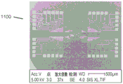
Examples of sensor devices fabricated according to the methods described above are shown in fig. 11A-11C, showing surface scanning electron micrographs of sensor device 1000 at 37 x, 5000 x, and 50,000 x magnification, respectively. The sensor device 1000 includes nanoelectrodes and nanocontacts for 20 sensors, as well as leads and pads for connection to an external ammeter. The pads and leads located on the surface of the substrate are clearly visible in fig. 11A. The sensor electrodes appear as the lighter vertical bands in the center of fig. 11B. In fig. 11C, the first electrode 1102 and the second electrode 1103 can be clearly seen, as well as the electrode gap 1120 defined between the first and second electrodes.
In various embodiments and referring now to fig. 9, a method of manufacturing a biomolecule sensing device can include a lithographic method 900 for manufacturing and/or determining contact positions. In various embodiments, the manufacturing method can begin with a microchip that includes a substrate on which a first electrode 802 and a second electrode 803 are disposed. The microchip may include a silicon substrate 880 covered with a silicon oxide layer 881 and a suitable resist layer 982. In the illustrated embodiment, e-beam lithography is used to expose a resist layer and define first contact location 985 and second contact location 986 in the resist layer (step 910). In various embodiments, the contact location can be defined to cover one of the first electrode and the second electrode, such as near a distal end of the electrode adjacent the electrode gap. As described below, defining the size and pattern of the contacts can help determine the size and shape of the contacts formed in later process steps. After the photolithography step, the resist is developed (step 920) to remove the resist in the contact locations defined in the photolithography step. Next, a deposition step (step 930) can be performed to form the first contact 906 and the second contact 907 on the first and second electrode surfaces. As for the electrodes, any suitable material and deposition method may be used. Similarly, any suitable substrate surface treatment may be performed prior to performing the deposition step, such as applying an intermediate attachment layer to provide a suitable bond between the electrode and the substrate. The contact can comprise a different material than the electrode, or the contact can comprise the same material used to fabricate the electrode. In various embodiments, the first and second contacts are made of gold using an electrochemical deposition method. After the depositing step, a stripping step (step 940) is performed to remove the remaining resist, leaving the first contact and the second contact disposed on the surfaces of the first and second electrodes.
Alternatively, in various embodiments, the method for fabricating the contact can include deposition of pre-fabricated contact nanoparticles. The pre-fabricated contact nanoparticles can be deposited into voids formed in the resist layer and configured to receive and position the contact nanoparticles at the contact locations, or the contact nanoparticles can be deposited using a chemically derivatized layer to enable attachment at the contact locations.
As shown in FIG. 10, a method 1000 of depositing pre-fabricated contact particles into voids formed in a resist layer can include the same steps of method 900 described above with respect to steps 910 and 920. After creating the void configured to receive the pre-formed contactor particle, a solution comprising a plurality of pre-formed contactor particles 1087 can be contacted with the device (step 1030) and the particles introduced into the void using pressure, mixing, surface tension, buoyancy, centrifugal force, or other methods. After the particles are deposited, excess solution and particles may be removed. A lift-off step, as described above with respect to step 940, can be performed to remove the remaining resist, and the pre-fabricated contact particles can then be optionally annealed to the electrodes as necessary to form securely attached first and second contacts (1006,1007).
Alternatively, a method of depositing the pre-fabricated contact nanoparticles using a chemical derivatization process can include steps similar to steps 910 and 920 described above with respect to the method shown in figure 9. For example, one widely used surface derivatization that is compatible with silicon substrate surfaces is silanization, which may include coating the substrate surface with molecules such as aminosilanes (e.g., APTES) or mercaptosilanes (e.g., MPTES). These molecules adhere to the silicon surface and then their exposed ends readily cross-link to other materials such as gold nanoparticles, thereby binding them to the surface. This derivatization process can then be applied rather than depositing contact metal or other materials in a step similar to step 930. After performing a peel-off step similar to step 940, the first and second electrodes will include surface derivatization at locations intended for attachment of the first and second contacts. A device comprising a derivatized electrode surface can be contacted with a solution comprising a plurality of preformed contact particles. The particles can have a surface or coating complementary to or specifically binding to the derivatized electrode surface, thereby localizing the haptic particles to the defined haptic locations. If desired, the derivatizing treatment and any particle coating can be removed in a removal step, and the pre-fabricated contact particles annealed to the electrode as described above. An example of such a method is the use of APTES-coated silicon surface-specific binding of gold nanoparticles.
In various embodiments, the contact structures can be created by various direct means, such as by positioning gold nanoparticle beads on the electrodes using Atomic Force Microscopy (AFM), or by depositing excess beads followed by removal of unwanted beads by AFM.
In various other implementations, the contact structures and/or electrode gaps can be formed in-situ by removing material, for example, using Focused Ion Beam (FIB) milling. For example, the electrode gap may be etched into a previously established continuous metal nanowire using FIB, thereby forming the first and second electrodes at the same time as the electrode gap is formed.
After the electrodes and contacts of the sensor or sensor array are fabricated, the sensor may be packaged in a flow cell or similar device adapted to allow the controlled introduction of a liquid solution into the sensor. Packaging the sensor chip in the flow cell is typically done by molding the flow cell with PDMS or other polymer or plastic and using it to surround the chip, with the fabricated electrodes and contacts properly exposed for bridge and probe assembly and subsequent assays using the complete sensor. In various embodiments, a surface passivation treatment may be applied to the substrate surface and to portions of the exposed electrodes to reduce electrical noise that may occur due to contact with the liquid sample. Passivation may be applied to leave the electrodes and/or contacts untreated in the region of the sensor gap. For example, in various embodiments, a 30nm wide region aligned with the sensor gap may not be processed. The passivation process may be performed before the sensor chip is packaged with the flow cell. A sensor according to various embodiments may have an electrical noise of less than about 1pA, or less than about 0.9pA, or less than about 0.8pA, or less than about 0.7pA, or less than about 0.6pA, or less than about 0.5pA, or less than about 0.4pA, or less than about 0.3pA, or less than about 0.2pA when a voltage of about 0.5V is applied and the sensor is immersed in a low ionic strength buffer solution suitable for supporting enzyme (e.g., DNA polymerase I enzyme) activity.
The manufacture of the biopolymer bridge can be performed by any of the various methods available for synthesizing biopolymer molecules, including in vivo synthetic methods, in vitro enzymatic synthetic methods, chemical synthetic methods, or any combination thereof. Various methods for producing biopolymer molecules suitable for use as bridge molecules according to the present disclosure are well known to those of ordinary skill in the art. Likewise, methods for derivatizing or modifying biopolymer bridge molecules to provide anchor or linker components as described herein are also well known. The various specific biopolymer bridge molecules described herein are provided by way of example and should not be construed as limiting the scope of the present disclosure, and synthetic bridge molecules may be used in accordance with various embodiments of the present disclosure.
In various embodiments, attachment of the biopolymer bridge molecule to the probe can be performed by a self-assembly chemical reaction. Likewise, attachment of the biopolymer bridge molecule to the electrode or contact may also be performed by a self-assembly chemical reaction. Such a self-assembly reaction may be carried out by bringing the two components to be attached into contact with each other via a solution comprising at least one component. In various embodiments, attachment of the biopolymer bridge to the probe can occur before, after, or simultaneously with attachment of the bridge to the electrode or contact. Similar considerations apply to bridge molecules generated by synthetic chemistry.
In various embodiments, a method of making a sensor device includes assembling a biopolymer bridge molecule to a first electrode and a second electrode. The bridge molecule assembly step may comprise a self-assembly step. The self-assembly may be performed by contacting the partially constructed sensor device comprising the first and second electrodes with a solution comprising the bridge molecule. The bridge molecule may self-assemble to the first and second electrodes based on the affinity between the first and second ends of the bridge molecule and the first and second electrodes. In various embodiments, the self-assembly of the sensor components can be monitored electronically by the sensor device, as described below in example 2 and with reference to fig. 13-15. Electronic monitoring can provide quality control functions and be used to identify sensors in properly assembled devices. Signals of sensor circuits that do not provide assembly process signals within predetermined parameters may be discarded in downstream analysis (e.g., sequencing analysis) using the device.
Example 1
Biopolymer bridge self-assembly
Using SEQ ID NO:1 and the oligonucleotide of SEQ ID NO: 2 to construct a double-stranded DNA biopolymer bridge molecule with an end-to-end length of about 20 nm. The bridge molecules were labeled using streptavidin-gold labels for visualization purposes. A test array 1200 (fig. 12) of gold nanoparticle contacts was fabricated using electron beam lithography to deposit pairs of gold contacts, each pair of contacts defining a center-to-center contact gap of about 20 nm. A buffer solution comprising gold-labeled bridge molecules is contacted with a test array of gold nanoparticle contacts. After a short incubation period, excess solution was removed, the array washed and imaged by Scanning Electron Microscopy (SEM). Fig. 12 shows an SEM image showing the arrangement of the gold touch 1270 and the gold tag 1271. For several pairs of haptics (indicated by arrows), gold labels 1271 disposed between the pairs of haptics can be seen, indicating successful self-assembly of the biomolecule bridge molecules to the pairs of haptics.
Example 2
Detecting self-assembly steps
A sensor device with a single sensor comprising gold contacts attached to electrodes with a center-to-center contact gap of about 20nm was fabricated using electron beam lithography. The sensor was encapsulated with a PDMS flow cell comprising a 1mm wide by 0.4mm high channel that was open at either end to allow liquid to be introduced into the first end of the flow cell interior and to drain from the second end of the flow cell, and the cell was in contact with the sensor solution. The direction of the flow cell channel is orthogonal to the direction of the electrodes containing the sensor, which is located approximately midway along the length of the flow cell channel. A low ionic strength buffer solution was introduced into the flow cell and a 0.5V potential was applied to the sensor throughout the following successive steps: introduction and self-assembly of double-stranded DNA bridge molecules (as described in example 1 above, but without gold tags) (fig. 13), introduction and binding of streptavidin-labeled Klenow fragments (fig. 14), introduction and binding of 50-base primed single-stranded DNA molecules (fig. 15), and introduction of dNTP mix to initiate template-based synthesis by Klenow fragments (fig. 16). The sequence of the DNA template molecule includes the following oligonucleotide sequences characterized by poly a regions:
5’-cgc cgc gga gcc aag aaa aaa aaa aaa aaa aaa aa ttgcatgtcctgtga-3’
and the primers used were:
3’-aac gta cag gac act-5’
in addition, similar sequences using poly C, G and T regions instead of the poly A region were used to study the effect of different template bases.
As shown in fig. 13, the measured current rises in three seconds. The two inflection points in the signal trace (a and B) are believed to correspond to the binding of the 5' -thiol-modified terminal base anchor to the first and second haptics. The signal traces after introduction of the solution containing streptavidin-labeled Klenow fragments (fig. 14) showed a sharp increase in current at about 1.5 seconds, which likely corresponds to the streptavidin linker component of the Klenow fragment enzyme contacting and binding the biotin linker component of the biopolymer bridge. In fig. 15, there is a sharp signal peak in the signal trace after introduction of the template strand into the flow cell, which peak is interpreted as template binding corresponding to Klenow fragment. FIG. 16 shows the signal traces measured after the introduction of a dNTP mix containing all the bases for DNA, again showing a significant signal signature at about 1 second. This may indicate that the synthesized duplex disassociates from the polymerase, and a signal trace of about 0.7 seconds to about 0.95 seconds may correspond to the kinetic signature generated by the sensor in response to nucleotide incorporation based on binding to the template DNA.
Example 3
Detection of nucleotide base incorporation
Sensor devices comprising biopolymer bridge molecules and Klenow fragment probes were fabricated and assembled as described in example 2 above. Signal traces are generated using a sensor device in response to DNA synthesis reactions performed using single-stranded DNA templates of different lengths and sequence compositions. Figure 17 shows a signal trace used to provide a template sequence incorporating a single base. The signal signature at 0.5 seconds was interpreted as corresponding to the templatedependent activity and base incorporation of the Klenow fragment, and the much weaker signal signature after 0.6 seconds was interpreted as corresponding to some form of noise or spurious signals in the system. FIG. 18 shows signal traces for various template regions. The template and primers described in example 2 above were used in the reactions shown.
The top and bottom signal traces are control experiments in which buffer without dntps is introduced into the sensor. Generating second, third and fourth signal traces (from top to bottom) in response to: dTTP (expected to result in 20 incorporation events directed by 20 a bases of template) is introduced into the solution, followed by dCTP (expected to allow 3 additional incorporations to be directed 3 'to 5' in the template by the GAA triplet), and then dNTP (expected to polymerize as directed by the remaining 12 bases of template), resulting in signals from 20, 3, and 12 incorporation events. Signal traces containing signal features located between the arrows of each signal trace are interpreted as corresponding to signal modulation caused by template-dependent enzyme activity. The relative duration of these perturbed signal regions is between 20: 3: 12, and a third such trace shows a clear spike that may correspond to 12 discrete inclusion events. FIG. 7 shows further examples of signal traces generated by DNA synthesis reactions using the above-described apparatus and the above-described template having 12 unpaired template bases. These results indicate that a sensor according to various embodiments can produce a signal trace comprising a signal characteristic responsive to template-dependent DNA polymerase probe activity. This also demonstrates the value of noise removal in clarifying signals: the upper graph of fig. 7 is the raw measurement signal and the lower graph has been signal processed to remove noise, in this case, the specific 60Hz line noise is eliminated by a band pass filter.
Example 4
Detection of methylated template bases
Sensor devices comprising biopolymer bridge molecules and Klenow fragment probes were fabricated and assembled as described in example 2 above. A signal trace is generated using a sensor device in response to DNA synthesis using a single-stranded DNA template comprising cytosine and 5-methylcytosine modified nucleotides. The template sequence comprises unpaired base nucleotides having the sequence 5 '-13 x (N) -5x (GmC) -5x (GC) -G-3' (i.e., 5 '-NNN NNN NNN NNN NGmC GmCG mCC GmCG CGC GCG CGC G-3' (SEQ ID NO:12), wherein N is any standard nucleotide, and wherein mC is 5-methylcytosine). The template sequence is designed to yield a template having the sequence 5' -C-5x (GC) -5x (GC) -13x (N) -3 '(i.e., 5' -CGC GCG CGC GC)G CGC GCG CGC NNN NNN NNN NNN N-3' (SEQ ID NO:13)), wherein the underlined guanosine base corresponds to the position of the 5-methylcytosine modified nucleotide in the template strand. A voltage of 0.5V was applied to the sensor and the current was measured all the way through the following successive introductions and incubations with it: water, buffer, dCTP buffer solution, dGTP buffer solution and buffer solution with a mixture of all four dNTP bases. The expected result would be a single dCTP incorporation event, followed by 20 dGTP and dCTP incorporation events, the first 10 of which are directed to unmodified cytosine bases, and the last 10 to 5-methylcytosine modified nucleotides. In the second 10 of these 20 events, the detection of methylation will show up as a different feature of the signal.
The signal traces generated during incubation with each reagent are shown in fig. 19. Incubation with water and buffer produced very low baseline currents with little change. Addition of a solution comprising dCTP resulted in a sharp sequence feature corresponding to the incorporation of a single base of dCTP for the template leader base G.
Addition of dGTP, resulting in a solution comprising both dCTP and dGTP, allows synthesis by 10 base incorporation corresponding to the unmodified nucleotide followed by synthesis by 10 base incorporation corresponding to the 5-methylcytosine base in the template strand. The signal trace produced during this incubation period showed a signal characteristic with a higher current from about 0.35 seconds to about 0.5 seconds followed by a signal characteristic with a lower current from about 0.5 seconds to about 0.65 seconds. This change in signal amplitude is interpreted as a significant change in the sensor signal in response to the effect of the methylation state of the template sequence on the polymerase and the resulting signal modulation. This evidence supports the ability of sensors according to various embodiments of the present disclosure to directly distinguish between the presence of modified nucleotides in a target sequence during a sequencing reaction.
Example 5
Detection of signals on reads of long DNA strands
Sensor devices comprising biopolymer bridge molecules and Klenow fragment probes were fabricated and assembled as described in example 2 above. In response to DNA synthesis using a single stranded DNA template comprising an approximately 5400bp template sequence derived from the genome of the phi X174 phage, a signal trace was generated using a sensor device. A dNTP mix was provided in the experimental sequencing reaction, along with a ddNTP (dideoxynucleotide triphosphate) mix for the control reaction. The ddNTP mix terminates the polymerization process after a single incorporation of such dideoxy terminator, and therefore produces substantially no sequencing-induced signal. These data were acquired at a sampling resolution of 20 milliseconds, which was too coarse to observe individual peak incorporations, but allowed the data to be collected over a period of 300 seconds long enough to observe the entire polymerization process at the expected enzyme rate of about 20 bases per second.
Figure 20 shows the signal traces resulting from experimental reactions of dNTP mix (upper signal trace) compared to the control reaction (lower trace) using ddNTP mix. The signal traces of the experimental sequencing runs included many different overall signal features (marked with arrows) that were absent in the control reactions and produced higher currents than the control reactions. The signal traces generated over the 100 second time period shown indicate that sensors according to various embodiments of the present disclosure may be adapted to generate a detectable signal in response to template-based nucleotide incorporation activity of a DNA polymerase probe during extended sequencing runs to obtain long template sequences. Thus, there is no direct limit to the length or template that such sensors can handle.
Other examples
Other non-limiting examples of the present disclosure include the following.
1. A sensor, comprising:
a first contact coupled to the first electrode;
a second contact coupled to the second electrode;
a sensor gap defined between one of the first contact and the first electrode and one of the second contact and the second electrode; and
a bridge molecule comprising a first end and a second end;
wherein the bridge molecule is a biopolymer bridge molecule; and
wherein the bridge molecule is coupled to the first contact at the first end and to the second contact at the second end.
2. A sensor, comprising:
a first electrode covering the surface of the substrate;
a second electrode covering the surface of the substrate;
a sensor gap defined between the first electrode and the second electrode; and
a bridge molecule comprising a first end and a second end;
wherein the sensor gap comprises a sensor gap dimension of about 5nm to about 30 nm; and
wherein the bridge molecule is coupled to the first contact at the first end and to the second contact at the second end.
3. The sensor of example 1 or 2, further comprising a gate electrode.
4. The sensor of example 1, wherein the sensor gap has a sensor gap dimension of about 5nm to about 30 nm.
5. The sensor of example 1 or 2, wherein the first end comprises a first self-assembling anchor, and/or the second end comprises a second self-assembling anchor.
6. The sensor of example 2, wherein the bridge molecule comprises a biopolymer bridge molecule.
7. The sensor of any one of examples 1-6, wherein the bridge molecule comprises a chemically synthesized bridge molecule.
8. The sensor of any one of examples 1-7, wherein the bridge molecule comprises a linear biopolymer.
9. The sensor of any one of examples 1-8, wherein the bridge molecule comprises an end-to-end length that is less than a persistence length of the bridge molecule.
10. The sensor of any one of examples 1-9, wherein the bridge molecule comprises an end-to-end length configured to approximate the sensor gap dimension.
11. The sensor of any one of examples 1-10, wherein the bridge molecule comprises a nucleic acid duplex.
12. The sensor of example 11, wherein the nucleic acid duplex comprises one of a DNA duplex, a DNA-RNA hybridization duplex, a DNA-PNA hybridization duplex, a PNA-PNA duplex, and a DNA-LNA hybridization duplex.
13. The sensor of example 11, wherein the nucleic acid duplex comprises a thiol-modified oligonucleotide.
14. The sensor of any one of examples 6-13, wherein one of the first self-assembling anchor and the second self-assembling anchor comprises a 5' -thiol modified nucleotide.
15. The sensor of example 11, wherein the nucleic acid duplex further comprises internal biotin-modified nucleotides.
16. The sensor of any one of examples 1-15, wherein the bridge molecule comprises a peptide sequence, and wherein one of the first self-assembling anchor and the second self-assembling anchor comprises an L-cysteine residue.
17. The sensor of any one of examples 1-16, wherein the bridge molecules are configured to self-assemble to produce a conformation of the bridge molecules when a fluid medium comprising the bridge molecules is contacted with one of the first contact and the second contact.
18. The sensor of any one of examples 1-17, further comprising a probe, wherein the probe is attached to the bridge molecule.
19. The sensor of any one of examples 1-18, further comprising a linker attached to the bridge molecule.
20. The sensor of any one of examples 18-19, wherein the probe is configured to bind to a single target molecule.
21. The sensor of any one of examples 1-20, wherein the molecular bridge and/or probe comprises an enzyme.
22. The sensor of example 21, wherein the enzyme is one of a polymerase and a reverse transcriptase.
23. The sensor of any one of examples 20-22, wherein the target molecule comprises a plurality of target molecule features, each target molecule feature having a discrete location, comprising a first target molecule feature at a first location, a second target molecule feature at a second location, and an nth target molecule feature at an nth location.
24. The sensor of example 18, wherein the probe is an enzyme configured to engage a plurality of different target molecules during a reaction in a solution comprising the target molecules, wherein the reaction comprises a time period t, and wherein contact of the target molecules produces a plurality of conformational changes in the enzyme responsive to the plurality of target molecule characteristics, wherein each of the plurality of conformational changes modulates current in the sensor to produce a signal characteristic.
25. A system comprising the sensor of any one of examples 1-24.
26. The system of claim 25, further comprising a signal processing system coupled to the sensor and configured to detect the signal characteristic.
27. The system of any of examples 25-26 or the sensor of any of examples 1-24, wherein the sensor is configured to generate a signal trace comprising a plurality of signal features detected over a time period t.
28. The system of any of examples 25-27, further comprising a signal interpretation apparatus.
29. The system of example 28, wherein the signal interpretation means comprises a signal interpretation map.
30. The system of any one of examples 28-29, wherein the signal interpretation map is calibrated against signal traces from known target sequences.
31. The system of any of examples 28-30, wherein the signal interpretation device is configured to return a signal interpretation in response to the signal trace produced by a target sequence.
32. The system of any of examples 28-31, wherein the signal interpretation comprises a probabilistic evaluation of a likelihood that the signal trace interpretation matches a possible actual sequence.
33. A method, the method comprising:
providing a sensor as in any one of examples 1-24, 27;
contacting the nucleic acid template with a polymerase, wherein the polymerase is coupled to a bridge molecule comprising a portion of the sensor;
optionally applying an electrical potential to the sensor;
providing a mixture of nucleotide bases;
performing an incorporation event by a polymerase comprising incorporation of a nucleotide from the nucleotide base mixture into the synthesized nucleic acid; and
a signal resulting from the incorporation event is detected.
34. The method of example 33, further comprising a series of inclusion events performed over a time period t, wherein the series of inclusion events produces a signal trace comprising a sequence of signal features.
35. The method of example 34, wherein each signal feature corresponds to one of a series of inclusion events.
36. The method of any of examples 34-35, wherein the signal trace further comprises noise, and wherein the method further comprises removing the noise from the signal trace.
37. The method of any one of examples 34-36, wherein each incorporation event generates template base-dependent polymerase kinetic profiles.
38. The method of any one of examples 34-37, wherein a polymerase kinetic signature contributes to a signal signature.
39. The method of any one of examples 33-38, wherein the method is adapted to distinguish between a first signal feature generated in response to an unmodified template nucleotide and a second signal feature generated in response to a modified template nucleotide.
40. The method of example 39, wherein the modified template nucleotide is N6-methyladenosine, N4-one of methylcytosine, 5-hydroxymethylcytosine, 5-formylcytosine and 5-carboxycytosine.
41. The method of example 39, wherein the modified template nucleotide is an abasic site.
42. A method of manufacturing a biomolecule sensing device, comprising:
forming a first electrode and a second electrode on a surface of a substrate, wherein the first electrode and the second electrode are separated by an electrode gap;
placing a first contact on the first electrode and a second contact on the second electrode, wherein the first contact and the second contact are separated by a contact gap; and
a bridge molecule is attached to the first contact and the second contact.
43. The method of example 42 further comprising contacting the bridge molecule with a probe to couple the probe to the bridge molecule, wherein the probe is coupled to the bridge molecule by self-assembly.
44. The method of any of examples 42-43, wherein attaching the bridge molecule to the first contact and the second contact comprises a self-assembly step.
45. The method of any of examples 42-44, wherein the electrode gap and/or the contact gap is about 5nm to about 30 nm.
46. The method of any of examples 42-45, wherein the first contact and/or the second contact comprise gold nanoparticles having a diameter of about 5 nm.
47. The method of any of examples 42-46, wherein the first contact position and/or the second contact position are determined using a lithographic method.
48. The method of any one of examples 42-47; further comprising placing a photoresist layer on the substrate surface including the first electrode and the second electrode, and defining a first contact location and a second contact location using a photolithographic method.
49. The method of any one of examples 42-48, further comprising applying a surface derivatization treatment to the substrate surface at the first contact position and the second contact position.
50. The method of example 49, wherein the surface derivatization treatment comprises silanization.
51. The method of any of examples 42-50, further comprising depositing a layer of gold and performing a lift-off step to dispose a first gold contact on the first electrode and/or a second gold contact on the second electrode.
52. The method of any of examples 42-51, further comprising contacting the device with a solution comprising a plurality of gold nanoparticles, and introducing a first gold nanoparticle at the first contact location and/or introducing a second gold particle at the second contact location.
53. The method of any of examples 42-52, wherein the bridge molecule attaches to the first contact and the second contact by self-assembly prior to contacting the bridge molecule with a probe or the probe.
54. The method of any one of examples 42-53, wherein prior to attaching the bridge molecule to the first contact and the second contact by self-assembly, the bridge molecule is contacted with the probe to form a sensor complex by self-assembly.
55. The method of any of examples 42-54, further comprising fabricating an integrated circuit electronically coupled to the first electrode and the second electrode.
56. The method of example 55, wherein the integrated circuit, the first electrode, and the second electrode comprise a mixed signal integrated circuit.
57. The method of example 56, wherein the integrated circuit, the first electrode, and the second electrode are fabricated using CMOS fabrication methods.
58. The method of any of examples 42-57, wherein the first and second contacts are fabricated using a CMOS fabrication method.
59. The method of any of examples 55-58, wherein the integrated circuit, the first electrode, and the second electrode are fabricated using a fabrication method suitable for fabricating a field effect transistor.
Benefits, other advantages, and solutions to problems have been described herein with regard to specific examples. Furthermore, the connecting lines shown in the various figures contained herein are intended to represent example functional relationships and/or physical couplings between the various elements. It should be noted that many alternative or additional functional relationships or physical connections may be provided in a practical system. However, the benefits, advantages, solutions to problems, and any element(s) that may cause any benefit, advantage, or solution to occur or become more pronounced are not to be construed as a critical, required, or essential feature or element of the invention. The scope of the invention is, therefore, indicated only by the appended claims, in which reference to an element in the singular is not intended to mean "one and only one" unless explicitly so stated, but rather "one or more". Furthermore, where a phrase similar to "at least one of a, B, or C" is used in a claim, it is intended that the phrase be interpreted to mean that a may be present alone in an embodiment, B may be present alone in an embodiment, C may be present alone in an embodiment, or any combination of elements a, B, and C may be present in a single embodiment; for example A and B, A and C, B and C, or A and B and C.
Different cross-hatching is used throughout the drawings to represent different parts, but not necessarily the same or different materials.
Systems, methods, and devices are provided herein. In the detailed description herein, references to "one embodiment," "an example embodiment," etc., indicate that the embodiment described may include a particular feature, structure, or characteristic, but every embodiment may not necessarily include the particular feature, structure, or characteristic. Moreover, such phrases are not necessarily referring to the same embodiment. Further, when a particular feature, structure, or characteristic is described in connection with an embodiment, it is submitted that it is within the knowledge of one skilled in the art to affect such feature, structure, or characteristic in connection with other embodiments whether or not explicitly described. Although various examples and embodiments described herein relate to methods of signal detection associated with nucleic acid targets, the devices and methods of the present disclosure are in no way limited to applications involving nucleic acid detection and sequencing. Similarly, while the various examples and embodiments described herein relate to sensors comprising biopolymer bridge molecules, chemically synthesized bridge molecules are within the scope of the present disclosure. After reading this description, it will become apparent to one skilled in the relevant art how to implement the disclosure in alternative embodiments.
Furthermore, no element, component, or method step in the present disclosure is intended to be dedicated to the public regardless of whether the element, component, or method step is explicitly recited in the claims. Claim elements herein should not be construed according to the provisions of article 112 (f) of the united states patent law, except where the phrase "device for … …" is used to specifically recite the element. As used herein, the terms "comprises," "comprising," or any other variation thereof, are intended to cover a non-exclusive inclusion, such that a process, method, article, or apparatus that comprises a list of elements does not include only those elements but may include other elements not expressly listed or inherent to such process, method, article, or apparatus.
Claims (22)
1. A sensor, comprising:
a first contact coupled to the first electrode;
a second contact coupled to the second electrode;
a sensor gap defined between one of the first contact and the first electrode and one of the second contact and the second electrode;
a bridge molecule comprising a first end and a second end; and
a polymerase attached to the bridge molecule;
wherein the bridge molecule is a biopolymer;
wherein the bridge molecule is coupled to the first contact at the first end and to the second contact at the second end;
wherein the polymerase is configured to undergo a conformational change that modulates current through the bridge molecule; and
wherein the polymerase is configured to attach to the bridge molecule through a self-assembling linker.
2. A sensor, comprising:
a first electrode covering the surface of the substrate;
a second electrode covering the surface of the substrate;
a sensor gap defined between the first electrode and the second electrode;
a bridge molecule comprising a first end and a second end; and
a polymerase attached to the bridge molecule;
wherein the sensor gap comprises a sensor gap size of 5nm to 30 nm;
wherein the bridge molecule is coupled to the first contact at the first end and to the second contact at the second end;
wherein the polymerase is configured to undergo a conformational change that modulates current through the bridge molecule; and
wherein the polymerase is configured to attach to the bridge molecule through a self-assembling linker.
3. The sensor of claim 1 or 2, wherein the first end comprises a first self-assembling anchor and the second end comprises a second self-assembling anchor.
4. The sensor of claim 2, wherein the bridge molecule comprises a chemically synthesized bridge molecule.
5. The sensor of claim 2, wherein the bridge molecule comprises a biopolymer bridge molecule.
6. The sensor of claim 2, wherein the bridge molecule comprises an end-to-end length configured to approximate the sensor gap dimension.
7. The sensor of claim 1 or 5, wherein the biopolymer bridge molecule comprises a nucleic acid duplex.
8. The sensor of claim 7, wherein the nucleic acid duplex comprises one of a DNA duplex, a DNA-RNA hybrid duplex, a DNA-PNA hybrid duplex, a PNA-PNA duplex, and a DNA-LNA hybrid duplex.
9. The sensor of claim 8, wherein the nucleic acid duplex further comprises internal biotin-modified nucleotides.
10. The sensor of claim 3, wherein the bridge molecule is configured to self-assemble to the first contact and the second contact to generate a bridge molecule conformation when a fluid medium containing the bridge molecule is contacted with one of the first contact and the second contact.
11. The sensor of claim 1 or 2, wherein the polymerase is configured to bind a single target molecule.
12. The sensor of claim 11, wherein the target molecule comprises a plurality of target molecule features, each target molecule feature having a discrete location, including a first target molecule feature at a first location, a second target molecule feature at a second location, and an nth target molecule feature at an nth location.
13. The sensor of claim 12, wherein the polymerase is configured to engage a plurality of different target molecules during a reaction in a solution comprising the target molecules, wherein the reaction comprises a time period t, and wherein contact of the target molecules produces a plurality of conformational changes in the polymerase responsive to the plurality of target molecule characteristics, wherein each of the plurality of conformational changes modulates current in the sensor to produce a signal characteristic.
14. A method of performing a nucleic acid sequencing reaction, the method comprising:
providing a sensor according to claim 1 or 2;
contacting a polymerase with a nucleic acid template;
applying an electrical potential to the sensor;
providing a mixture of nucleotide bases;
performing an incorporation event by a polymerase comprising incorporation of a nucleotide from the nucleotide base mixture into the synthesized nucleic acid;
a signal resulting from the incorporation event is detected.
15. The method of claim 14, further comprising a series of inclusion events performed over a time period t, wherein the series of inclusion events produces a signal trace comprising a sequence of signal features, each signal feature corresponding to one event in the series of inclusion events.
16. The method of claim 15, wherein the method distinguishes between a first signal feature generated in response to an unmodified template nucleotide and a second signal feature generated in response to a modified template nucleotide.
17. A method of manufacturing a biomolecule sensing device, comprising:
forming a first electrode and a second electrode on a surface of a substrate, wherein the first electrode and the second electrode are separated by an electrode gap;
placing a first contact on the first electrode and a second contact on the second electrode, wherein the first contact and the second contact are separated by a contact gap;
attaching a bridge molecule to the first contact and the second contact; and
attaching a polymerase to the bridge molecule,
wherein the polymerase is configured to undergo a conformational change that modulates current through the bridge molecule.
18. The method of claim 17, wherein attaching the bridge molecule to the first contact and the second contact comprises a self-assembly step.
19. The method of claim 17, wherein the electrode gap and the contact gap are between 5nm and 30 nm.
20. The method of claim 17, further comprising fabricating an integrated circuit electronically coupled to the first electrode and the second electrode.
21. The method of claim 20, wherein the integrated circuit, the first electrode, and the second electrode are fabricated using CMOS fabrication methods.
22. The method of claim 17, wherein the first and second contacts are fabricated using CMOS fabrication methods.
Applications Claiming Priority (3)
| Application Number | Priority Date | Filing Date | Title |
|---|---|---|---|
| US201562184776P | 2015-06-25 | 2015-06-25 | |
| US62/184,776 | 2015-06-25 | ||
| PCT/US2016/039446 WO2016210386A1 (en) | 2015-06-25 | 2016-06-24 | Biomolecular sensors and methods |
Publications (2)
| Publication Number | Publication Date |
|---|---|
| CN108027335A CN108027335A (en) | 2018-05-11 |
| CN108027335B true CN108027335B (en) | 2021-05-04 |
Family
ID=57586591
Family Applications (1)
| Application Number | Title | Priority Date | Filing Date |
|---|---|---|---|
| CN201680049272.8A Active CN108027335B (en) | 2015-06-25 | 2016-06-24 | Biomolecule sensor and method |
Country Status (7)
| Country | Link |
|---|---|
| US (2) | US10036064B2 (en) |
| EP (1) | EP3314245A4 (en) |
| JP (1) | JP7166586B2 (en) |
| KR (1) | KR20180054558A (en) |
| CN (1) | CN108027335B (en) |
| CA (1) | CA3021580A1 (en) |
| WO (1) | WO2016210386A1 (en) |
Families Citing this family (64)
| Publication number | Priority date | Publication date | Assignee | Title |
|---|---|---|---|---|
| US10527494B2 (en) * | 2014-09-26 | 2020-01-07 | Korea Intitute of Machinery & Materials | Substrate on which multiple nanogaps are formed, and manufacturing method therefor |
| US10379102B2 (en) | 2015-12-11 | 2019-08-13 | Arizona Board Of Regents On Behalf Of Arizona State University | System and method for single molecule detection |
| CN113985017A (en) * | 2016-01-14 | 2022-01-28 | 罗斯韦尔生物技术股份有限公司 | Molecular sensors and related methods |
| WO2017132567A1 (en) | 2016-01-28 | 2017-08-03 | Roswell Biotechnologies, Inc. | Massively parallel dna sequencing apparatus |
| CN109071212A (en) * | 2016-01-28 | 2018-12-21 | 罗斯韦尔生物技术股份有限公司 | Use the method and apparatus of large-scale molecular electronic sensor array measurement analyte |
| US10737263B2 (en) | 2016-02-09 | 2020-08-11 | Roswell Biotechnologies, Inc. | Electronic label-free DNA and genome sequencing |
| US10597767B2 (en) | 2016-02-22 | 2020-03-24 | Roswell Biotechnologies, Inc. | Nanoparticle fabrication |
| GB201609221D0 (en) | 2016-05-25 | 2016-07-06 | Oxford Nanopore Tech Ltd | Method |
| US9829456B1 (en) | 2016-07-26 | 2017-11-28 | Roswell Biotechnologies, Inc. | Method of making a multi-electrode structure usable in molecular sensing devices |
| US20210139959A1 (en) | 2016-08-01 | 2021-05-13 | Roswell Biotechnologies, Inc. | Modified nucleotide triphosphates for molecular electronic sensors |
| GB201620450D0 (en) | 2016-12-01 | 2017-01-18 | Oxford Nanopore Tech Ltd | Method |
| US10902939B2 (en) | 2017-01-10 | 2021-01-26 | Roswell Biotechnologies, Inc. | Methods and systems for DNA data storage |
| EP3571286A4 (en) | 2017-01-19 | 2020-10-28 | Roswell Biotechnologies, Inc | Solid state sequencing devices comprising two dimensional layer materials |
| JP2018151324A (en) * | 2017-03-14 | 2018-09-27 | 東芝テック株式会社 | Ion sensor chip |
| WO2018200687A1 (en) | 2017-04-25 | 2018-11-01 | Roswell Biotechnologies, Inc. | Enzymatic circuits for molecular sensors |
| US10508296B2 (en) | 2017-04-25 | 2019-12-17 | Roswell Biotechnologies, Inc. | Enzymatic circuits for molecular sensors |
| GB201707140D0 (en) | 2017-05-04 | 2017-06-21 | Oxford Nanopore Tech Ltd | Method |
| KR102606670B1 (en) * | 2017-05-09 | 2023-11-24 | 로스웰 바이오테크놀로지스 인코포레이티드 | Coupled probe circuits for molecular sensors |
| EP3676389A4 (en) | 2017-08-30 | 2021-06-02 | Roswell Biotechnologies, Inc | Processive enzyme molecular electronic sensors for dna data storage |
| KR20200067871A (en) | 2017-10-10 | 2020-06-12 | 로스웰 바이오테크놀로지스 인코포레이티드 | Methods, devices and systems for storing amplified DNA data |
| RU2679494C1 (en) | 2017-12-26 | 2019-02-11 | Ооо "Гамма-Днк" | Method of non-marking single-molecular sequency of dna and device for its implementation |
| GB2573323A (en) * | 2018-05-03 | 2019-11-06 | Mursia Ltd | Biosensor method and system |
| KR20210045361A (en) * | 2018-05-17 | 2021-04-26 | 레커그니션 어낼러틱스 엘엘씨 | Apparatus, system and method for direct electrical measurement of enzyme activity |
| GB201809323D0 (en) | 2018-06-06 | 2018-07-25 | Oxford Nanopore Tech Ltd | Method |
| NL2021376B1 (en) * | 2018-06-29 | 2020-01-06 | Illumina Inc | Sensor and sensing system |
| US11621345B2 (en) * | 2018-08-14 | 2023-04-04 | Pawan Tyagi | Systems and methods of fabricating gate electrode on trenched bottom electrode based molecular spintronics device |
| JP7158969B2 (en) * | 2018-09-18 | 2022-10-24 | 株式会社東芝 | Organic probes and molecular detectors |
| CN109443609B (en) * | 2018-10-29 | 2020-10-16 | 陕西科技大学 | High-precision piezoresistive sensor material based on collagen and preparation method thereof |
| US11493499B1 (en) | 2018-10-30 | 2022-11-08 | Seagate Technology Llc | Event timing detection for DNA sequencing |
| WO2020101795A1 (en) | 2018-11-15 | 2020-05-22 | Omniome, Inc. | Electronic detection of nucleic acid structure |
| WO2020113138A1 (en) * | 2018-11-29 | 2020-06-04 | Universal Sequencing Technology | A system for sequencing biopolymers |
| US10710076B2 (en) | 2018-12-04 | 2020-07-14 | Omniome, Inc. | Mixed-phase fluids for nucleic acid sequencing and other analytical assays |
| EP3908832A4 (en) * | 2019-01-10 | 2023-07-19 | Roswell Biotechnologies Inc. | Conductive synthetic peptides for molecular electronics |
| US20220099615A1 (en) * | 2019-01-18 | 2022-03-31 | Universal Sequencing Technology Corporation | Devices, Methods, and Chemical Reagents for Biopolymer Sequencing |
| US20220106638A1 (en) * | 2019-02-08 | 2022-04-07 | Universal Sequencing Technology Corporation | Peptide Nanostructure for Biopolymer Sensing |
| US11499189B2 (en) | 2019-02-14 | 2022-11-15 | Pacific Biosciences Of California, Inc. | Mitigating adverse impacts of detection systems on nucleic acids and other biological analytes |
| US20220186294A1 (en) * | 2019-04-15 | 2022-06-16 | Universal Sequencing Technology Corporation | Nanogap Device for Biopolymer Identification |
| RU2724507C1 (en) * | 2019-08-30 | 2020-06-23 | Ооо "Гамма-Днк" | Method of detecting dna polymerisation reaction result and a device for implementation thereof |
| TW202124406A (en) | 2019-09-10 | 2021-07-01 | 美商歐姆尼歐美公司 | Reversible modification of nucleotides |
| DE202019106694U1 (en) | 2019-12-02 | 2020-03-19 | Omniome, Inc. | System for sequencing nucleic acids in fluid foam |
| GB201917742D0 (en) | 2019-12-04 | 2020-01-15 | Oxford Nanopore Tech Ltd | Method |
| US20230054204A1 (en) | 2020-02-04 | 2023-02-23 | Pacific Biosciences Of California, Inc. | Flow cells and methods for their manufacture and use |
| AU2021228647A1 (en) | 2020-02-28 | 2022-09-22 | Arizona Board Of Regents On Behalf Of Arizona State University | Methods for sequencing biopolymers |
| AU2021269556A1 (en) * | 2020-05-11 | 2022-10-27 | Illumina, Inc. | Devices including particles coupled to electrodes, and methods of making and using the same |
| EP4165549A1 (en) | 2020-06-11 | 2023-04-19 | Nautilus Biotechnology, Inc. | Methods and systems for computational decoding of biological, chemical, and physical entities |
| JP2023530155A (en) | 2020-06-18 | 2023-07-13 | オックスフォード ナノポール テクノロジーズ ピーエルシー | Methods for Characterizing Polynucleotides Translocating Through Nanopores |
| GB202009349D0 (en) | 2020-06-18 | 2020-08-05 | Oxford Nanopore Tech Ltd | Method |
| US20230295712A1 (en) | 2020-06-18 | 2023-09-21 | Oxford Nanopore Technologies Plc | A method of selectively characterising a polynucleotide using a detector |
| US20220003756A1 (en) * | 2020-06-22 | 2022-01-06 | Roswell Biotechnologies, Inc. | Methods for bonding molecules to ruthenium surfaces |
| EP4193363A1 (en) | 2020-08-07 | 2023-06-14 | Oxford Nanopore Technologies plc | Methods of identifying nucleic acid barcodes |
| KR20230118570A (en) | 2020-11-11 | 2023-08-11 | 노틸러스 서브시디어리, 인크. | Affinity reagents with enhanced binding and detection properties |
| WO2022159663A1 (en) | 2021-01-21 | 2022-07-28 | Nautilus Biotechnology, Inc. | Systems and methods for biomolecule preparation |
| CN112881473B (en) * | 2021-01-25 | 2022-06-21 | 中国地质大学(武汉) | DNA monomolecular device capable of identifying adriamycin through inserting layer and application thereof |
| WO2022164989A2 (en) * | 2021-01-27 | 2022-08-04 | Pleno, Inc. | Microfluidics systems, devices, and methods |
| JP2024514405A (en) | 2021-03-11 | 2024-04-02 | ノーティラス・サブシディアリー・インコーポレイテッド | Systems and methods for biomolecule retention |
| WO2023038859A1 (en) | 2021-09-09 | 2023-03-16 | Nautilus Biotechnology, Inc. | Characterization and localization of protein modifications |
| WO2023049073A1 (en) | 2021-09-22 | 2023-03-30 | Nautilus Biotechnology, Inc. | Methods and systems for determining polypeptide interactions |
| WO2023081728A1 (en) | 2021-11-03 | 2023-05-11 | Nautilus Biotechnology, Inc. | Systems and methods for surface structuring |
| GB202118908D0 (en) | 2021-12-23 | 2022-02-09 | Oxford Nanopore Tech Ltd | Method |
| GB202118906D0 (en) | 2021-12-23 | 2022-02-09 | Oxford Nanopore Tech Ltd | Method |
| WO2023192917A1 (en) | 2022-03-29 | 2023-10-05 | Nautilus Subsidiary, Inc. | Integrated arrays for single-analyte processes |
| WO2023222657A1 (en) | 2022-05-17 | 2023-11-23 | Oxford Nanopore Technologies Plc | Method and adaptors |
| WO2023250364A1 (en) | 2022-06-21 | 2023-12-28 | Nautilus Subsidiary, Inc. | Method for detecting analytes at sites of optically non-resolvable distances |
| WO2024073599A1 (en) | 2022-09-29 | 2024-04-04 | Nautilus Subsidiary, Inc. | Preparation of array surfaces for single-analyte processes |
Citations (10)
| Publication number | Priority date | Publication date | Assignee | Title |
|---|---|---|---|---|
| WO2002074985A2 (en) * | 2001-03-20 | 2002-09-26 | Infineon Technologies Ag | Method of detecting macromolecular biopolymers by means of an electrode arrangement |
| US20030064390A1 (en) * | 1999-12-13 | 2003-04-03 | Schuelein Jurgen | Method and device for detecting and quantifying biomolecules |
| WO2003042396A2 (en) * | 2001-06-11 | 2003-05-22 | Genorx, Inc. | Electronic detection of biological molecules using thin layers |
| WO2005108612A2 (en) * | 2003-11-28 | 2005-11-17 | Genorx, Inc. | Nanoscale biosensor device, system and technique |
| US20100184062A1 (en) * | 2007-07-04 | 2010-07-22 | Rho-Best Coating Hartstoffbeschichtigungs Gmbh | Method for Identifying and Quantifying Organic and Biochemical Substances |
| US20140048776A1 (en) * | 2012-08-17 | 2014-02-20 | National Chiao Tung University | Protein transistor device |
| US20140079592A1 (en) * | 2012-09-19 | 2014-03-20 | National Chiao Tung University | Bio-nanowire device and method of fabricating the same |
| WO2014182630A1 (en) * | 2013-05-06 | 2014-11-13 | Pacific Biosciences Of California , Inc. | Real-time electronic sequencing |
| CN104685066A (en) * | 2012-04-09 | 2015-06-03 | 一龙公司 | Compositions and methods for quantifying a nucleic acid sequence in a sample |
| CN104703700A (en) * | 2012-08-06 | 2015-06-10 | 康特姆斯集团有限公司 | Method and kit for nucleic acid sequencing |
Family Cites Families (146)
| Publication number | Priority date | Publication date | Assignee | Title |
|---|---|---|---|---|
| US5082627A (en) | 1987-05-01 | 1992-01-21 | Biotronic Systems Corporation | Three dimensional binding site array for interfering with an electrical field |
| US5486449A (en) | 1989-02-07 | 1996-01-23 | Rohm Co., Ltd. | Photomask, photoresist and photolithography for a monolithic IC |
| GB2244135B (en) | 1990-05-04 | 1994-07-13 | Gen Electric Co Plc | Sensor devices |
| US6051380A (en) | 1993-11-01 | 2000-04-18 | Nanogen, Inc. | Methods and procedures for molecular biological analysis and diagnostics |
| IL103674A0 (en) | 1991-11-19 | 1993-04-04 | Houston Advanced Res Center | Method and apparatus for molecule detection |
| US5366140A (en) | 1993-09-30 | 1994-11-22 | Minnesota Mining And Manufacturing Company | Patterned array of uniform metal microbeads |
| US5871918A (en) | 1996-06-20 | 1999-02-16 | The University Of North Carolina At Chapel Hill | Electrochemical detection of nucleic acid hybridization |
| US5583359A (en) | 1995-03-03 | 1996-12-10 | Northern Telecom Limited | Capacitor structure for an integrated circuit |
| US5639507A (en) | 1995-05-03 | 1997-06-17 | Avx Corporation | Method of making a planar multi-layer capacitor |
| EP0876601B1 (en) | 1995-12-01 | 2004-07-14 | Innogenetics N.V. | Impedimetric detection system and method of production thereof |
| US6033582A (en) | 1996-01-22 | 2000-03-07 | Etex Corporation | Surface modification of medical implants |
| US6506564B1 (en) * | 1996-07-29 | 2003-01-14 | Nanosphere, Inc. | Nanoparticles having oligonucleotides attached thereto and uses therefor |
| US6202471B1 (en) | 1997-10-10 | 2001-03-20 | Nanomaterials Research Corporation | Low-cost multilaminate sensors |
| US6110354A (en) | 1996-11-01 | 2000-08-29 | University Of Washington | Microband electrode arrays |
| US7169272B2 (en) | 1997-04-30 | 2007-01-30 | Board Of Trustees Of The University Of Arkansas | Microfabricated recessed disk microelectrodes: characterization in static and convective solutions |
| US5982018A (en) | 1997-05-23 | 1999-11-09 | Micron Technology, Inc. | Thin film capacitor coupons for memory modules and multi-chip modules |
| FR2764386B1 (en) | 1997-06-06 | 1999-07-16 | Commissariat Energie Atomique | ELECTRODES HOLDER COMPRISING AT LEAST ONE ELECTRODE COVERED BY A DEPOSIT AND READING SYSTEM THEREOF |
| US6123819A (en) | 1997-11-12 | 2000-09-26 | Protiveris, Inc. | Nanoelectrode arrays |
| US6537747B1 (en) | 1998-02-03 | 2003-03-25 | Lucent Technologies Inc. | Data transmission using DNA oligomers |
| JP2002517300A (en) | 1998-06-10 | 2002-06-18 | ジョージア テック リサーチ コーポレイション | Microneedle devices and methods of manufacture and uses thereof |
| US6094335A (en) | 1998-10-09 | 2000-07-25 | Advanced Micro Devices, Inc. | Vertical parallel plate capacitor |
| WO2000050232A1 (en) | 1999-02-25 | 2000-08-31 | Seiko Epson Corporation | Structure member excellent in water-repellency and manufacturing method thereof |
| US6517669B2 (en) | 1999-02-26 | 2003-02-11 | Micron Technology, Inc. | Apparatus and method of detecting endpoint of a dielectric etch |
| ATE408141T1 (en) | 1999-10-20 | 2008-09-15 | Shigeori Takenaka | GENE DETECTION CHIP, SENSOR AND DETECTION METHOD |
| DE10015818A1 (en) | 2000-03-30 | 2001-10-18 | Infineon Technologies Ag | Biosensor and method for determining macromolecular biopolymers using a biosensor |
| CA2406133A1 (en) | 2000-04-17 | 2001-10-25 | Rashid Bashir | Biosensor and related method |
| AU2001261145B2 (en) | 2000-05-03 | 2005-08-11 | The United States Government, As Represented By The Department Of The Navy | Biological identification system with integrated sensor chip |
| US6670131B2 (en) | 2000-11-30 | 2003-12-30 | Kabushiki Kaisha Toshiba | Nucleic acid detection method and apparatus, and vessel for detecting nucleic acid |
| NL1016779C2 (en) | 2000-12-02 | 2002-06-04 | Cornelis Johannes Maria V Rijn | Mold, method for manufacturing precision products with the aid of a mold, as well as precision products, in particular microsieves and membrane filters, manufactured with such a mold. |
| DE10063739B4 (en) | 2000-12-21 | 2009-04-02 | Ferro Gmbh | Substrates with self-cleaning surface, process for their preparation and their use |
| US6958216B2 (en) | 2001-01-10 | 2005-10-25 | The Trustees Of Boston College | DNA-bridged carbon nanotube arrays |
| US6749731B2 (en) | 2001-01-31 | 2004-06-15 | Kyocera Corporation | Gene detection chip and detection device |
| CA2451882A1 (en) | 2001-03-14 | 2002-09-19 | University Of Massachusetts | Nanofabrication |
| US6824974B2 (en) * | 2001-06-11 | 2004-11-30 | Genorx, Inc. | Electronic detection of biological molecules using thin layers |
| US20040023253A1 (en) * | 2001-06-11 | 2004-02-05 | Sandeep Kunwar | Device structure for closely spaced electrodes |
| US7297494B2 (en) * | 2001-06-25 | 2007-11-20 | Georgia Tech Research Corporation | Activatable probes and methods for in vivo gene detection |
| AU2002354569A1 (en) | 2001-07-12 | 2003-01-29 | Merck And Co., Inc. | Electrical field stimulation of eukaryotic cells |
| US6483125B1 (en) | 2001-07-13 | 2002-11-19 | North Carolina State University | Single electron transistors in which the thickness of an insulating layer defines spacing between electrodes |
| US6861224B2 (en) | 2001-11-02 | 2005-03-01 | Fujitsu Limited | Protein detecting device |
| JP2006501486A (en) | 2002-05-14 | 2006-01-12 | ナノスフェアー インコーポレイテッド | Electrical detection of DNA hybridization and specific binding events |
| CN1723575A (en) | 2002-06-05 | 2006-01-18 | 瑞威欧公司 | Layered electrochemical cell and manufacturing method therefor |
| EP1376111A1 (en) | 2002-06-24 | 2004-01-02 | Universite Catholique De Louvain | Method and device for high sensitivity detection of the presence of DNA and other probes |
| US7470533B2 (en) | 2002-12-20 | 2008-12-30 | Acea Biosciences | Impedance based devices and methods for use in assays |
| DE10242560A1 (en) | 2002-09-13 | 2004-03-25 | Creavis Gesellschaft Für Technologie Und Innovation Mbh | Process for preparation of self-cleaning surfaces on coated flat textile structures useful for cladding technical textiles and structures obtained from these and production of raincoats and safety clothing with signaling effect |
| US20040063100A1 (en) | 2002-09-30 | 2004-04-01 | Wang Chung Lin | Nanoneedle chips and the production thereof |
| DE10247679A1 (en) * | 2002-10-12 | 2004-04-22 | Fujitsu Ltd., Kawasaki | Semiconductor body structure, as a biosensor, has two thick layers of one material separated by a thin different intermediate layer forming a nano gap, with organic wire structures as the contacts |
| US7183055B2 (en) | 2002-11-01 | 2007-02-27 | Wisconsin Alumni Research Foundation | Direct radio-frequency detection of nucleotide hybridization at microelectrodes |
| WO2005005679A2 (en) | 2003-04-28 | 2005-01-20 | Nanosys, Inc. | Super-hydrophobic surfaces, methods of their construction and uses therefor |
| JP4059181B2 (en) | 2003-09-29 | 2008-03-12 | 株式会社村田製作所 | Manufacturing method of multi-terminal type multilayer ceramic electronic components |
| JP2005109269A (en) | 2003-09-30 | 2005-04-21 | Hitachi Ltd | Semiconductor radiation detector and semiconductor radiation imager |
| CA2547544C (en) | 2003-12-16 | 2013-04-02 | Dynabyte Informationssysteme Gmbh | Cartridge device for blood analysis |
| US7451381B2 (en) | 2004-02-03 | 2008-11-11 | Phonex Broadband Corporation | Reliable method and system for efficiently transporting dynamic data across a network |
| US20050247573A1 (en) | 2004-03-23 | 2005-11-10 | Hideaki Nakamura | Biosensors |
| US7385295B2 (en) | 2004-06-24 | 2008-06-10 | California Institute Of Technology | Fabrication of nano-gap electrode arrays by the construction and selective chemical etching of nano-crosswire stacks |
| US7265019B2 (en) | 2004-06-30 | 2007-09-04 | International Business Machines Corporation | Elastomeric CMOS based micro electromechanical varactor |
| US7258731B2 (en) | 2004-07-27 | 2007-08-21 | Ut Battelle, Llc | Composite, nanostructured, super-hydrophobic material |
| US7150904B2 (en) | 2004-07-27 | 2006-12-19 | Ut-Battelle, Llc | Composite, ordered material having sharp surface features |
| US7655275B2 (en) | 2004-08-02 | 2010-02-02 | Hewlett-Packard Delopment Company, L.P. | Methods of controlling flow |
| US20060029808A1 (en) | 2004-08-06 | 2006-02-09 | Lei Zhai | Superhydrophobic coatings |
| US7507320B2 (en) | 2004-10-09 | 2009-03-24 | Academia Sinica | Single-atom tip and preparation method thereof |
| KR20070045255A (en) | 2004-10-14 | 2007-05-02 | 가부시끼가이샤 도시바 | Fet-based nucleic acid detecting sensor |
| DE102004060738B4 (en) | 2004-12-15 | 2008-07-03 | Forschungszentrum Jülich GmbH | Process for the structured application of molecules to a conductor track |
| WO2006132694A2 (en) | 2005-04-01 | 2006-12-14 | Clemson University | Ultrahydrophobic substrates |
| US7417418B1 (en) | 2005-06-14 | 2008-08-26 | Ayliffe Harold E | Thin film sensor |
| WO2007053242A2 (en) | 2005-09-19 | 2007-05-10 | Wayne State University | Transparent hydrophobic article having self-cleaning and liquid repellant features and method of fabricating same |
| FR2893266B1 (en) | 2005-11-14 | 2007-12-21 | Commissariat Energie Atomique | SUPERHYDROPHIL OR SUPERHYDROPHOBIC PRODUCT, PROCESS FOR PRODUCING THE SAME AND USE THEREOF |
| KR100757389B1 (en) | 2005-12-06 | 2007-09-11 | 한국전자통신연구원 | Sensors having nano-gap electrode and their manufacturing method |
| WO2007133288A1 (en) | 2005-12-15 | 2007-11-22 | The Trustees Of Columbia University In The City Of New York | Sensing devices from molecular electronic devices utilizing hexabenzocoronenes |
| US7649198B2 (en) | 2005-12-28 | 2010-01-19 | Industrial Technology Research Institute | Nano-array and fabrication method thereof |
| WO2007087377A2 (en) | 2006-01-25 | 2007-08-02 | Massachusetts Institute Of Technology | Photoelectrochemical synthesis of high density combinatorial polymer arrays |
| WO2007102960A2 (en) | 2006-01-30 | 2007-09-13 | Ashland Licensing And Intellectual Property Llc | Hydrophobic self-cleaning coating compositions |
| US20070184247A1 (en) | 2006-02-03 | 2007-08-09 | Simpson John T | Transparent, super-hydrophobic, disordered composite material |
| US8105469B2 (en) | 2006-03-17 | 2012-01-31 | Andrew John Whitehead | Microelectrode array |
| US20090011222A1 (en) | 2006-03-27 | 2009-01-08 | Georgia Tech Research Corporation | Superhydrophobic surface and method for forming same |
| US20070227300A1 (en) | 2006-03-31 | 2007-10-04 | Quantumsphere, Inc. | Compositions of nanometal particles containing a metal or alloy and platinum particles for use in fuel cells |
| US20070231542A1 (en) | 2006-04-03 | 2007-10-04 | General Electric Company | Articles having low wettability and high light transmission |
| GB2437328A (en) | 2006-04-10 | 2007-10-24 | Cambridge Display Tech Ltd | Electric devices and methods of manufacture |
| JP2008026109A (en) | 2006-07-20 | 2008-02-07 | Fujifilm Corp | Fine structure, its manufacturing method, sensor device and raman spectroscopic device |
| US20100194409A1 (en) | 2006-08-16 | 2010-08-05 | Agency For Science, Technology And Research | Method of electrically detecting a biological analyte molecule |
| JP4986138B2 (en) | 2006-11-15 | 2012-07-25 | 独立行政法人産業技術総合研究所 | Method for manufacturing mold for optical element having antireflection structure |
| GB0625070D0 (en) | 2006-12-15 | 2007-01-24 | Imp Innovations Ltd | Characterization of molecules |
| KR100854486B1 (en) | 2007-04-05 | 2008-08-26 | 한국기계연구원 | Manufacturing method for super water-repellent surface |
| US8278188B2 (en) | 2007-07-19 | 2012-10-02 | University of Pittsburgh—of the Commonwealth System of Higher Education | Manipulation, detection, and assay of small scale biological particles |
| US20100285601A1 (en) | 2007-09-28 | 2010-11-11 | Agency For Science, Technology And Research | Method of electrically detecting a nucleic acid molecule |
| WO2009082706A1 (en) * | 2007-12-21 | 2009-07-02 | The Trustees Of Columbia University In The City Of New York | Active cmos sensor array for electrochemical biomolecular detection |
| US8372585B2 (en) | 2007-12-31 | 2013-02-12 | Intel Corporation | Electronic sensing for nucleic acid sequencing |
| US8183648B2 (en) * | 2008-01-25 | 2012-05-22 | Ut-Battelle, Llc | Nanoscopic electrode molecular probes |
| US20090297913A1 (en) | 2008-03-25 | 2009-12-03 | The University Of Georgia Research Foundation, Inc. | Nanostructure-Enhanced stereo-electrodes for fuel cells and biosensors |
| WO2009154710A2 (en) | 2008-06-19 | 2009-12-23 | Plexigen, Inc. | Multi-dimensional fluid sensors and related detectors and methods |
| US7970332B2 (en) | 2008-06-30 | 2011-06-28 | Xerox Corporation | Oil less fusing using nano/micro textured fusing surfaces |
| CN102150037B (en) | 2008-07-11 | 2014-06-04 | 康奈尔大学 | Nanofluidic channels with integrated charge sensors and methods based thereon |
| WO2010022107A2 (en) | 2008-08-18 | 2010-02-25 | The Regents Of The University Of California | Nanostructured superhydrophobic, superoleophobic and/or superomniphobic coatings, methods for fabrication, and applications thereof |
| US20100044212A1 (en) | 2008-08-21 | 2010-02-25 | Snu R&Db Foundation | Vertically standing ionic polymer-metal composite |
| US20100132771A1 (en) | 2008-10-06 | 2010-06-03 | The Regents Of The University Of California | 3D Carbon Nanotubes Membrane as a Solar Energy Absorbing Layer |
| US20100206367A1 (en) | 2009-02-18 | 2010-08-19 | Korea Institute Of Industrial Technology | Method for fabricating silicon nano wire, solar cell including silicon nano wire and method for fabricating solar cell |
| WO2010120809A1 (en) | 2009-04-14 | 2010-10-21 | Nanoink, Inc. | Conducting lines, nanoparticles, inks, and patterning |
| US20100285272A1 (en) | 2009-05-06 | 2010-11-11 | Shari Elizabeth Koval | Multi-length scale textured glass substrates for anti-fingerprinting |
| KR20110104245A (en) | 2010-03-16 | 2011-09-22 | 주식회사 나노플랫폼 | Fet based biosensor, method for manufacturing the same, and method for detecting target materials |
| US8940663B2 (en) | 2010-04-07 | 2015-01-27 | Board Of Regents, The University Of Texas System | Nano-scale biosensors |
| KR101136534B1 (en) | 2010-09-07 | 2012-04-17 | 한국기계연구원 | Probe card and manufacturing method thereof |
| US9231133B2 (en) | 2010-09-10 | 2016-01-05 | International Business Machines Corporation | Nanowires formed by employing solder nanodots |
| WO2012037118A2 (en) | 2010-09-14 | 2012-03-22 | The General Hospital Corporation | Nanoporous metal multiple electrode array and method of making same |
| US9956743B2 (en) | 2010-12-20 | 2018-05-01 | The Regents Of The University Of California | Superhydrophobic and superoleophobic nanosurfaces |
| EP2661775A1 (en) | 2011-01-04 | 2013-11-13 | Ecole Polytechnique Fédérale de Lausanne (EPFL) | Semiconductor device |
| US8652768B1 (en) | 2011-01-31 | 2014-02-18 | Sandia Corporation | Nanopatterns by phase separation of patterned mixed polymer monolayers |
| EP2492673A1 (en) * | 2011-02-28 | 2012-08-29 | Lexogen GmbH | Biosensor array formed by junctions of functionalized electrodes |
| KR102023754B1 (en) | 2011-07-27 | 2019-09-20 | 더 보오드 오브 트러스티스 오브 더 유니버시티 오브 일리노이즈 | Nanopore sensors for biomolecular characterization |
| WO2013018802A1 (en) | 2011-08-04 | 2013-02-07 | 日産化学工業株式会社 | Resist underlayer film-forming composition for euv lithography containing condensation polymer |
| US8685858B2 (en) | 2011-08-30 | 2014-04-01 | International Business Machines Corporation | Formation of metal nanospheres and microspheres |
| US20130108956A1 (en) | 2011-11-01 | 2013-05-02 | Az Electronic Materials Usa Corp. | Nanocomposite positive photosensitive composition and use thereof |
| KR101813907B1 (en) | 2011-12-15 | 2018-01-02 | 인텔 코포레이션 | Diamond electrode nanogap transducers |
| CA2859761C (en) | 2011-12-22 | 2023-06-20 | President And Fellows Of Harvard College | Compositions and methods for analyte detection |
| US20130183492A1 (en) | 2012-01-17 | 2013-07-18 | Snu R&Db Foundation | Metal nanoparticles on substrate and method of forming the same |
| US20130214875A1 (en) | 2012-02-16 | 2013-08-22 | Elwha Llc | Graphene sheet and nanomechanical resonator |
| US20130239349A1 (en) | 2012-03-14 | 2013-09-19 | Palo Alto Research Center Incorporated | Self-powered manual toothbrush with sensors |
| US9393590B2 (en) | 2012-04-16 | 2016-07-19 | Temple University—Of the Commonwealth System of Higher Education | Self-assembly of small structures |
| WO2013165588A1 (en) | 2012-05-01 | 2013-11-07 | Life Technologies Corporation | Methods for analysis of dna fragments |
| US9551682B2 (en) * | 2012-06-29 | 2017-01-24 | Intel Corporation | High throughput biochemical detection using single molecule fingerprinting arrays |
| WO2014013260A1 (en) | 2012-07-19 | 2014-01-23 | Oxford Nanopore Technologies Limited | Modified helicases |
| US8741688B2 (en) | 2012-07-24 | 2014-06-03 | Micron Technology, Inc. | Methods of forming a metal chalcogenide material |
| EP2912695A4 (en) | 2012-10-26 | 2016-07-06 | Res Triangle Inst | Intermediate band semiconductors, heterojunctions, and optoelectronic devices utilizing solution processed quantum dots, and related methods |
| WO2014097943A1 (en) | 2012-12-18 | 2014-06-26 | 東レ株式会社 | Metal dot substrate and method for manufacturing metal dot substrate |
| US20140218637A1 (en) | 2013-02-06 | 2014-08-07 | Nanchang O-Film Tech. Co., Ltd. | Conductive film, manufacturing method thereof, and touch screen including the conducting film |
| CN103187119B (en) | 2013-02-06 | 2014-08-06 | 南昌欧菲光科技有限公司 | Conductive film, preparation method for conductive film and touch screen comprising conductive film |
| US8901621B1 (en) | 2013-06-18 | 2014-12-02 | International Business Machines Corporation | Nanochannel process and structure for bio-detection |
| CN104252498B (en) * | 2013-06-28 | 2019-05-03 | Sap欧洲公司 | Context-aware is recommended |
| TW201502276A (en) * | 2013-07-09 | 2015-01-16 | Univ Nat Chiao Tung | Sequencing method for label-free single molecular nucleic acid |
| US20150049332A1 (en) | 2013-07-30 | 2015-02-19 | The Curators Of The University Of Missouri | Gold nanoisland arrays |
| US9683958B2 (en) * | 2013-09-11 | 2017-06-20 | Agilent Technologies, Inc. | Nanofluidic device for charge analysis of straightened molecules |
| US20160284811A1 (en) | 2013-11-04 | 2016-09-29 | Massachusetts Institute Of Technology | Electronics including graphene-based hybrid structures |
| US9472396B2 (en) | 2014-04-15 | 2016-10-18 | University Of Central Florida Research Foundation, Inc. | Plasma treated semiconductor dichalcogenide materials and devices therefrom |
| CN106471359A (en) | 2014-04-28 | 2017-03-01 | 量子生物有限公司 | Nano-gap electrode device and system and forming method thereof |
| EP2947779A1 (en) | 2014-05-23 | 2015-11-25 | Thomson Licensing | Method and apparatus for storing information units in nucleic acid molecules and nucleic acid storage system |
| CA2950960A1 (en) | 2014-06-06 | 2015-12-10 | Solstice Biologics, Ltd. | Polynucleotide constructs having bioreversible and non-bioreversible groups |
| CA2955356C (en) | 2014-07-15 | 2024-01-02 | Illumina, Inc. | Biochemically activated electronic device |
| GB2528682A (en) | 2014-07-28 | 2016-02-03 | Isis Innovation | Plasmonic filter |
| US9859513B2 (en) | 2014-11-25 | 2018-01-02 | University Of Kentucky Research Foundation | Integrated multi-terminal devices consisting of carbon nanotube, few-layer graphene nanogaps and few-layer graphene nanoribbons having crystallographically controlled interfaces |
| US20160187282A1 (en) | 2014-12-26 | 2016-06-30 | Intel Corporation | Device for single molecule detection and fabrication methods thereof |
| KR20180072717A (en) | 2015-10-08 | 2018-06-29 | 퀀텀 바이오시스템즈 가부시키가이샤 | Apparatus, system and method for nucleic acid sequencing |
| CN113985017A (en) | 2016-01-14 | 2022-01-28 | 罗斯韦尔生物技术股份有限公司 | Molecular sensors and related methods |
| CN109071212A (en) | 2016-01-28 | 2018-12-21 | 罗斯韦尔生物技术股份有限公司 | Use the method and apparatus of large-scale molecular electronic sensor array measurement analyte |
| WO2017132567A1 (en) | 2016-01-28 | 2017-08-03 | Roswell Biotechnologies, Inc. | Massively parallel dna sequencing apparatus |
| US10737263B2 (en) | 2016-02-09 | 2020-08-11 | Roswell Biotechnologies, Inc. | Electronic label-free DNA and genome sequencing |
| US10597767B2 (en) | 2016-02-22 | 2020-03-24 | Roswell Biotechnologies, Inc. | Nanoparticle fabrication |
| WO2017184677A1 (en) | 2016-04-21 | 2017-10-26 | President And Fellows Of Harvard College | Method and system of nanopore-based information encoding |
| US9829456B1 (en) | 2016-07-26 | 2017-11-28 | Roswell Biotechnologies, Inc. | Method of making a multi-electrode structure usable in molecular sensing devices |
-
2016
- 2016-06-24 EP EP16815467.2A patent/EP3314245A4/en active Pending
- 2016-06-24 KR KR1020187002256A patent/KR20180054558A/en not_active Application Discontinuation
- 2016-06-24 CA CA3021580A patent/CA3021580A1/en active Pending
- 2016-06-24 WO PCT/US2016/039446 patent/WO2016210386A1/en active Application Filing
- 2016-06-24 CN CN201680049272.8A patent/CN108027335B/en active Active
- 2016-06-24 JP JP2017566864A patent/JP7166586B2/en active Active
- 2016-10-27 US US15/336,557 patent/US10036064B2/en active Active
-
2018
- 2018-06-18 US US16/011,065 patent/US20180340220A1/en not_active Abandoned
Patent Citations (10)
| Publication number | Priority date | Publication date | Assignee | Title |
|---|---|---|---|---|
| US20030064390A1 (en) * | 1999-12-13 | 2003-04-03 | Schuelein Jurgen | Method and device for detecting and quantifying biomolecules |
| WO2002074985A2 (en) * | 2001-03-20 | 2002-09-26 | Infineon Technologies Ag | Method of detecting macromolecular biopolymers by means of an electrode arrangement |
| WO2003042396A2 (en) * | 2001-06-11 | 2003-05-22 | Genorx, Inc. | Electronic detection of biological molecules using thin layers |
| WO2005108612A2 (en) * | 2003-11-28 | 2005-11-17 | Genorx, Inc. | Nanoscale biosensor device, system and technique |
| US20100184062A1 (en) * | 2007-07-04 | 2010-07-22 | Rho-Best Coating Hartstoffbeschichtigungs Gmbh | Method for Identifying and Quantifying Organic and Biochemical Substances |
| CN104685066A (en) * | 2012-04-09 | 2015-06-03 | 一龙公司 | Compositions and methods for quantifying a nucleic acid sequence in a sample |
| CN104703700A (en) * | 2012-08-06 | 2015-06-10 | 康特姆斯集团有限公司 | Method and kit for nucleic acid sequencing |
| US20140048776A1 (en) * | 2012-08-17 | 2014-02-20 | National Chiao Tung University | Protein transistor device |
| US20140079592A1 (en) * | 2012-09-19 | 2014-03-20 | National Chiao Tung University | Bio-nanowire device and method of fabricating the same |
| WO2014182630A1 (en) * | 2013-05-06 | 2014-11-13 | Pacific Biosciences Of California , Inc. | Real-time electronic sequencing |
Also Published As
| Publication number | Publication date |
|---|---|
| US20170044605A1 (en) | 2017-02-16 |
| JP2018522236A (en) | 2018-08-09 |
| US20180340220A1 (en) | 2018-11-29 |
| US10036064B2 (en) | 2018-07-31 |
| EP3314245A1 (en) | 2018-05-02 |
| CA3021580A1 (en) | 2016-12-29 |
| JP7166586B2 (en) | 2022-11-08 |
| WO2016210386A1 (en) | 2016-12-29 |
| CN108027335A (en) | 2018-05-11 |
| EP3314245A4 (en) | 2019-02-27 |
| KR20180054558A (en) | 2018-05-24 |
Similar Documents
| Publication | Publication Date | Title |
|---|---|---|
| CN108027335B (en) | Biomolecule sensor and method | |
| CN109416334B (en) | Molecular sensors and related methods | |
| Mu et al. | Silicon nanowire field-effect transistors—A versatile class of potentiometric nanobiosensors | |
| Chen et al. | Electrical nanogap devices for biosensing | |
| Balasubramanian | Challenges in the use of 1D nanostructures for on-chip biosensing and diagnostics: A review | |
| US8236595B2 (en) | Nanowire sensor, nanowire sensor array and method of fabricating the same | |
| US20090155800A1 (en) | Biosensor having nano wire and manufacturing method thereof | |
| US9880126B2 (en) | Biosensor based on carbon nanotube-electric field effect transistor and method for producing the same | |
| US20200393440A1 (en) | Method, apparatus and system for single-molecule polymerase biosensor with transition metal nanobridge | |
| EP2434278A1 (en) | Apparatus for detecting one or more analytes comprising an elongated nano-structure and method for manufacturing said apparatus | |
| JP4927319B2 (en) | Biochip manufacturing method using high-density carbon nanotube film or pattern | |
| Tey et al. | Nanotubes-/nanowires-based, microfluidic-integrated transistors for detecting biomolecules | |
| WO2021237180A1 (en) | Near-room-temperature processable amorphous semiconductor nano-ribbon bridge biosensors and memory devices | |
| Delle et al. | Scalable fabrication and application of nanoscale IDE-arrays as multi-electrode platform for label-free biosensing | |
| KR20100113698A (en) | A biosensor based on carbonnanotube-field effect transistor and a method for producing thereof | |
| Chen et al. | Nanotechnology: moving from microarrays toward nanoarrays | |
| JP5069343B2 (en) | Carbon nanotube-field effect transistor based biosensor and method of manufacturing the same | |
| Shanbhag et al. | Nanostructured electrodes | |
| US20220170879A1 (en) | Tunable nanopillar and nanogap electrode structures and methods thereof | |
| Carrara et al. | New probe immobilizations by Lipoate-Diethalonamines or ethylene-glycol molecules for capacitance DNA chip | |
| Fortina et al. | Beyond Microtechnology—Nanotechnology in Molecular Diagnosis | |
| Zaffino et al. | Electrochemical DNA Biosensors at the Nanoscale | |
| Zou et al. | A NANO INTERDIGITATED ELECTRODES ARRAY ON POLYMER FOR DISPOSABLE IMPEDIMETRIC BIOSENSORS | |
| Huang | Patterned fabrication of polyaniline nanostructures for ultrasensitive biomolecule detection |
Legal Events
| Date | Code | Title | Description |
|---|---|---|---|
| PB01 | Publication | ||
| PB01 | Publication | ||
| SE01 | Entry into force of request for substantive examination | ||
| SE01 | Entry into force of request for substantive examination | ||
| GR01 | Patent grant | ||
| GR01 | Patent grant |