CN1080098A - The hige efficiency class D amplifier of Zero-voltage complementary switching - Google Patents
The hige efficiency class D amplifier of Zero-voltage complementary switching Download PDFInfo
- Publication number
- CN1080098A CN1080098A CN93106002A CN93106002A CN1080098A CN 1080098 A CN1080098 A CN 1080098A CN 93106002 A CN93106002 A CN 93106002A CN 93106002 A CN93106002 A CN 93106002A CN 1080098 A CN1080098 A CN 1080098A
- Authority
- CN
- China
- Prior art keywords
- amplifier
- conversion
- discharge lamp
- transformer
- transistor
- Prior art date
- Legal status (The legal status is an assumption and is not a legal conclusion. Google has not performed a legal analysis and makes no representation as to the accuracy of the status listed.)
- Granted
Links
- 230000000295 complement effect Effects 0.000 title description 2
- 238000006243 chemical reaction Methods 0.000 claims description 38
- 230000006698 induction Effects 0.000 claims description 11
- 230000010355 oscillation Effects 0.000 claims description 2
- 238000007789 sealing Methods 0.000 claims 1
- 239000003990 capacitor Substances 0.000 description 13
- 238000004804 winding Methods 0.000 description 10
- 230000008878 coupling Effects 0.000 description 6
- 238000010168 coupling process Methods 0.000 description 6
- 238000005859 coupling reaction Methods 0.000 description 6
- 230000003247 decreasing effect Effects 0.000 description 3
- 238000010586 diagram Methods 0.000 description 3
- 239000007789 gas Substances 0.000 description 3
- 239000000843 powder Substances 0.000 description 3
- QSHDDOUJBYECFT-UHFFFAOYSA-N mercury Chemical compound [Hg] QSHDDOUJBYECFT-UHFFFAOYSA-N 0.000 description 2
- 229910052753 mercury Inorganic materials 0.000 description 2
- 230000005855 radiation Effects 0.000 description 2
- 238000005096 rolling process Methods 0.000 description 2
- 240000006829 Ficus sundaica Species 0.000 description 1
- 230000005540 biological transmission Effects 0.000 description 1
- 239000011248 coating agent Substances 0.000 description 1
- 238000000576 coating method Methods 0.000 description 1
- 239000003814 drug Substances 0.000 description 1
- 230000000694 effects Effects 0.000 description 1
- 230000005672 electromagnetic field Effects 0.000 description 1
- 238000005516 engineering process Methods 0.000 description 1
- 230000005284 excitation Effects 0.000 description 1
- 230000005669 field effect Effects 0.000 description 1
- 238000007667 floating Methods 0.000 description 1
- 239000011521 glass Substances 0.000 description 1
- 239000011261 inert gas Substances 0.000 description 1
- 229910044991 metal oxide Inorganic materials 0.000 description 1
- 150000004706 metal oxides Chemical class 0.000 description 1
- 230000006855 networking Effects 0.000 description 1
- 230000035699 permeability Effects 0.000 description 1
- 239000007787 solid Substances 0.000 description 1
- 238000002211 ultraviolet spectrum Methods 0.000 description 1
Images

Classifications
-
- H—ELECTRICITY
- H05—ELECTRIC TECHNIQUES NOT OTHERWISE PROVIDED FOR
- H05B—ELECTRIC HEATING; ELECTRIC LIGHT SOURCES NOT OTHERWISE PROVIDED FOR; CIRCUIT ARRANGEMENTS FOR ELECTRIC LIGHT SOURCES, IN GENERAL
- H05B41/00—Circuit arrangements or apparatus for igniting or operating discharge lamps
- H05B41/14—Circuit arrangements
- H05B41/26—Circuit arrangements in which the lamp is fed by power derived from DC by means of a converter, e.g. by high-voltage DC
- H05B41/28—Circuit arrangements in which the lamp is fed by power derived from DC by means of a converter, e.g. by high-voltage DC using static converters
- H05B41/2806—Circuit arrangements in which the lamp is fed by power derived from DC by means of a converter, e.g. by high-voltage DC using static converters with semiconductor devices and specially adapted for lamps without electrodes in the vessel, e.g. surface discharge lamps, electrodeless discharge lamps
- H05B41/2813—Arrangements for protecting lamps or circuits against abnormal operating conditions
-
- H—ELECTRICITY
- H03—ELECTRONIC CIRCUITRY
- H03F—AMPLIFIERS
- H03F3/00—Amplifiers with only discharge tubes or only semiconductor devices as amplifying elements
- H03F3/20—Power amplifiers, e.g. Class B amplifiers, Class C amplifiers
- H03F3/21—Power amplifiers, e.g. Class B amplifiers, Class C amplifiers with semiconductor devices only
- H03F3/217—Class D power amplifiers; Switching amplifiers
- H03F3/2171—Class D power amplifiers; Switching amplifiers with field-effect devices
-
- Y—GENERAL TAGGING OF NEW TECHNOLOGICAL DEVELOPMENTS; GENERAL TAGGING OF CROSS-SECTIONAL TECHNOLOGIES SPANNING OVER SEVERAL SECTIONS OF THE IPC; TECHNICAL SUBJECTS COVERED BY FORMER USPC CROSS-REFERENCE ART COLLECTIONS [XRACs] AND DIGESTS
- Y02—TECHNOLOGIES OR APPLICATIONS FOR MITIGATION OR ADAPTATION AGAINST CLIMATE CHANGE
- Y02B—CLIMATE CHANGE MITIGATION TECHNOLOGIES RELATED TO BUILDINGS, e.g. HOUSING, HOUSE APPLIANCES OR RELATED END-USER APPLICATIONS
- Y02B20/00—Energy efficient lighting technologies, e.g. halogen lamps or gas discharge lamps
Landscapes
- Engineering & Computer Science (AREA)
- Power Engineering (AREA)
- Circuit Arrangements For Discharge Lamps (AREA)
- Amplifiers (AREA)
Abstract
The present invention relates to a kind of hige efficiency class D amplifier.This amplifier includes two transistors, changes break-make in regular turn.Its output is by exporting on the common node between two transistors.Really make each transistor when it is connected, voltage is substantially 0 on it, and this moment, the efficient of amplifier greatly increased.This advantage is obtained via connect the mode of an inductance on common node, and the electric energy that is stored in any stray capacitance was all transferred on the inductance before arbitrary transistor is connected.
Description
The present invention relates to the D class A amplifier A, especially relate to hige efficiency class D amplifier, these amplifiers are suitable for providing high-frequency signal to give the interior induction coil of electrodeless discharge lamp.
The citation form of D class A amplifier A as shown in Figure 1.Two transistor Q
AAnd Q
BBy transformer driven be transformed in connect with shutoff between and make each other mutually that phasic difference is 180 °.These two transistors are equivalent to the double-pole switch shown in Fig. 2, and produce square wave output on its common node, and waveform is similar shown in this waveform and Fig. 3.
It is desirable to, the efficient of D class A amplifier A should be 100%, that is, and and at transistor Q
AAnd Q
BWhen repeating to change break-make again, should be fully consumed power not.But, in fact, transistor Q
AAnd Q
BItself all have it and reside in resistance, be commonly referred to the transistorized resistance that resides in.These transistors also have its natural capacity, are capacitor C as shown in fig. 1
AAnd C
B, these capacitors are can charge and produce voltage when it turn-offs.Therefore, when it was connected, because of voltage difference is arranged, the result flows through, and to enable quantitative change be that heat scatters and disappears to transistorized electric current on the transistor.This energy loss can be expressed as CV
2F, C wherein represent that (its value is C to transistorized natural capacity
AOr C
B), V is VD (V
DD), and the frequency of f when to be amplifier drive.In fact, the standard operation efficient of high frequency D class A amplifier A is about 50% to 60%.The major part of this loss in efficiency is owing to the transistor natural capacity causes.This poor efficiency, for the unaffordable electrodeless discharge lamp of remarkable power loss and other devices, the adaptability of D class A amplifier A is restricted greatly.
In real work, has the transistor Q of same electrical characteristic
AAnd Q
B, be not turning on and off immediately with simultaneously shown in Fig. 3.Otherwise, from the sinusoidal waveform of the input standard of transformer, when it arrives its threshold voltage V
ThThe time each transistor is connected, as shown in Figure 4.Therefore, between another transistor connection there is in one of them shutoff of transistor a time period.Therefore, its output signal is not to be complete square wave, and the overbank time is arranged, and as shown in Figure 5, its time period is △ t.In addition, each transistorized turning on and off must have the regular hour.
The object of the present invention is to provide a kind of D class A amplifier A of high efficiency.
Another object of the present invention is to provide a kind of electrodeless discharge lamp that uses this D class A amplifier A.
In order to reach the foregoing invention purpose, a kind of D class A amplifier A of the present invention comprises:
First and second conversion equipments of series connection;
In order to control first gating device of first conversion equipment;
In order to control second gating device of second conversion equipment;
A signal source that is connected to first gating device and second gating device, this signal source disconnects described first conversion equipment and described second conversion equipment in proper order and is closed, first and second conversion equipments one of them when disconnecting, another is closed, and also have a time period, first and second conversion equipments are disconnection in this time period;
Wherein, described amplifier has intrinsic electric capacity, when one of them disconnects when first and second conversion equipments, and intrinsic electric capacity storage power; And
The device of storage power, this device receive the energy that is stored in the natural capacity in the described time period, so that reduce the voltage that is added on first and second conversion equipments, make it almost nil under the situation that transfers closure from disconnection to.
Of the present invention another uses the electrodeless discharge lamp of D class A amplifier A, comprising:
A source oscillation signal;
A near induction coil that is installed to the sealer, described airtight container contains metallic vapour, and,
An amplifier that is connected with described induction coil, described amplifier comprises:
First and second conversion equipments of series connection;
Be used for disconnecting in succession first gating device with closed first conversion equipment;
Be used for disconnecting in succession second gating device with closed second conversion equipment
Wherein (ⅰ) described amplifier has been designed to a time period, in this time period, is disconnection at first and second conversion equipments, and
(ⅱ) described amplifier has an intrinsic electric capacity, storage power when this electric capacity is disconnection at first and second conversion equipments;
The device of a storage power, this device receives the energy that is stored in the described natural capacity, be added in the voltage of first and second conversion equipments on one of them so that reduce, make under one of them situation when disconnection is transformed into closure of first and second conversion equipments voltage almost nil.
In D class A amplifier A of the present invention, the inherent inductance of amplifier is to be coupled on two common nodes between transistor according to capacitive way.This inductance in fact with transistorized natural capacity and circuit on other stray capacitances constitute a resonant circuit, these electric capacity are generically and collectively referred to as output capacitance C
oSelecting of inductance, in the time period △ t when two transistors all turn-off, it is stored in output capacitance C
oInterior power transfer is to inductance.Therefore when a transistor turn-offs, at output capacitance C
oAnd energy takes place between the inductance shift, and another transistor does not have voltage drop when connecting on it.As mentioned above, Here it is makes the loss of transistor transfer power be decreased to the bottom line conditions needed.
Therefore, the resonant circuit that constituted of inductance and output capacitance is transferred on the inductance energy that is stored in the output capacitance thus, consumes and be unlikely when transistor is connected via current flowing and thermal loss.
The principle of the invention is specially adapted to such as electrodeless discharge lamp device, and wherein for the whole efficiency of lamp significantly, the power loss the when oscillator signal that is transferred to induction coil is amplified is reduced to bottom line.
Below in conjunction with drawings and Examples the present invention is described in further detail.
Brief Description Of Drawings:
Figure 1 shows that traditional D class A amplifier A circuit diagram.
Figure 2 shows that the equivalent electric circuit of D class A amplifier A.
Figure 3 shows that the idealized output of D class output amplifier.
Figure 4 shows that by the input of signal source to the D class A amplifier A.
Figure 5 shows that when transfer lag counted the output of D class A amplifier A.
Figure 6 shows that D class A amplifier A circuit diagram of the present invention.
Figure 7 shows that the transformer in the D class A amplifier A of Fig. 6.
Figure 8 shows that the overlapped view of the input and output signal of D class A amplifier A.
Figure 9 shows that the resonant circuit in the D class A amplifier A of Fig. 6.
Figure 10 shows that the calcspar that D class A amplifier A of the present invention is connected with electrodeless discharge lamp.
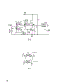
Figure 6 shows that hige efficiency class D amplifier circuit diagram of the present invention.Signal source S carries sinusoidal wave input signal, R
SThe impedance of expression signal source S.This input signal is transported to transformer device T
1, this assembly comprises transformer T
1aAnd T
1b, shared same magnetic core CR, as shown in Figure 7.Transformer T
1aAnd T
1bEach winding is denoted as L in Fig. 6 and 7
a, L
b, L
cAnd L
d(L
a-L
dBe sometimes referred to as the self-induction of each indivedual winding) on.As shown in Figure 7, winding L
aAnd L
bFor two-wire around a side of rolling up in magnetic core CR, and winding L
cAnd L
dFor two-wire around rolling up in the opposite side of magnetic core CR.Winding L
aAnd L
b(transformer T
1a) between and winding L
cAnd L
d(transformer T
1b) between coupling near 1, simultaneously because transformer 1
1aAnd T
1bDistolateral on the contrary between magnetic core CR (being separated by 180 ° approximately), and because the magnetic permeability of magnetic core CR is extremely low.Coupling therebetween extremely low (standard about 0.5).Since following reason, transformer T
1aThe number of turn than transformer T
1bThe number of turn be many.
Translation function is via transistor Q
1And Q
2Institute provides, and each transistor is the N channel power metal oxide field-effect transistor (MOSFET) of turning.Transistor Q
1And Q
2Be series at DC power supply voltage V
DDAnd between the ground connection, transistor Q
1Source terminal and transistor Q
2Drain electrode end constitute common node, represent amplifier to export.This output feedback is transported on matched impedance networking N and the load L.The matched impedance network N has multiple variation, is well known to those skilled in the art.
Winding L
aTerminal E is via coupling capacitor C
1With transistor Q
1Grid be coupled.Winding L
bTerminal F is via coupling capacitor C
2With the coupling of output cross streams, and winding L
dTerminal D is via inductance L
1With transistor Q
2Gate terminal be connected.Capacitor C shown in Fig. 6
1, C
2And C
3All in order to as the ac coupling capacitor device.Capacitor C
4Exchange by-pass capacitor in order to conduct, to guarantee transistor Q
1AC impedance between drain electrode end and electric current ground connection is kept a minimum value.Resistor R
1And R
2Be connected in transistor Q respectively
1And Q
2Grid and source terminal between, and guarantee that it is on zero the basis that transistor gate remains on direct current.
Transformer T
1aConstitute balance one uneven transmission transformer, make signal inversion apply inversion signal in transistor Q from signal source S
1Grid on.(balance one balun sees that people such as Hao Baite L Crouse collaborates, the 374th page of Solid State Radio Engineering one book that father and son publishing house publishes in being defended by John in 1980, and included in this explanation for reference.) on the other hand, transformer T
1bBe common transformer, this transformer carries signal to give transistor Q
2Grid, this signal with from the signal homophase of signal source S.Therefore, when the signal from signal source S uprises, transformer T
1bThe output of D end also uprises, and makes transistor Q
2Connect.Simultaneously, from the output of transformer E end, be the benchmark step-down with the F end, make transistor Q
1Turn-off.Balance one balun T on the magnetic core CR
1aWith common transformer T
1bConfiguration according to shown in mode aid, make it as transistor Q
1And Q
2In one turn-off, and there is proper spacing the time of another transistor when connecting.In addition, inductance L
1Make and put on transistor Q
2The signal of grid produce phase delay, make transistor Q
1And Q
2All the shutoff some time (or makes transistor Q when output signal changes each time
1And Q
2Between the overlapping bottom line that is decreased to).
Be decorated with the capacitor C of dotted line
OIt is the whole output capacitance of expression amplifier.Therefore, this electric capacity comprises transistor Q
1And Q
2Natural capacity (intersect at the capacitor C among Fig. 1
AAnd C
B) and circuit in any other stray capacitance.
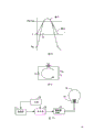
Figure 8 shows that input signal and the equitant view of output signal, and Figure 9 shows that the ideal form of institute's discovery resonant circuit in the D class A amplifier A from signal source S.Fig. 8 shows that especially input signal is less than arbitrary transistor Q
1And Q
2Threshold voltage V
ThTime period △ t.As indicated above, this is two time periods that transistor all turn-offs of expression.When in this situation, transistor Q
1And Q
2Between common node floating, and set up resonant circuit in fact.As shown in Figure 9, this resonant circuit includes capacitor C
O, inductor L
b(this is transformer T
1aA part), and by L
bAnd C
OThe equivalent series resistance R of the charging cycle path of being formed
cDeng, work as R
cThe value hour, the natural frequency f of this circuit
nCan regulate according to following relation:
Therefore, at transistor Q
1And Q
2When all turn-offing, capacitor C
OOn the electric charge that gathers begin via resonant circuit shown in Figure 9 the speed discharge that is determined according to the circuit natural frequency.Conditions needed is when transistor is connected, each transistor Q
1And Q
2On voltage will be O.C
OLast voltage is by+V
DDDrop to the O required time when natural frequency is Fn, be 1/4th of signal cycle duration.Therefore, as transistor Q
2During connection, C
OWhen last voltage must be for O, should obtain the relation of following formula:
△t= 1/(4f
n) (2)
Comprehensively (1) can obtain required L with (2) formula
bValue.
For keeping this relation, under stable state, when a transistor all turn-offs, be stored in C
OInterior energy is transferred to inductance L during △ t
bIn, but not the transistor Q for flowing through and connecting
1Or Q
2The electric current of middle one produces heat and loses.Stored energy is in C
OWith L
bBetween shift (" flywheel " effect) and unlikely losing back and forth.
In preferred embodiment, should obtain following relation:
L
a=L
b>>L
c=L
d
It is desirable to L
aOr L
bValue is about L
cOr L
dThe value ten times.The energy that is fed back to the common input node (A or C) by amplifier output is greatly decayed for this reason.Winding L
bAnd L
cIntersect at the voltage divider between output and circuit ground.As a result, the input driving power of supplying via signal source S is decreased to bottom line, makes amplifier show better stability simultaneously.Make winding L
cBe set in and winding L
bWhen relatively being suitable low value, make L
cThe Low ESR of value and signal source S when the counting circuit resonance frequency, can be ignored, as shown in Figure 9.And, L
cLow value make impedance on the common node because winding L
cLow ESR and obtain relative fixed.But, winding L
cAnd L
dAll should offer the enough impedances of signal source S.
D class A amplifier A of the present invention can be used with any kind device that needs high efficiency to amplify.And be particularly useful for electrodeless discharge lamp, as shown in Figure 10.Described in No. the 4th, 010,400, the United States Patent (USP) case, for reference, the electrodeless discharge lamp standard include induction coil, this coil is subjected to the high-frequency excitation and can energy is transferred on the admixture of gas via electromagnetic field.This admixture of gas comprises mercury vapour and inert gas, all includes in the closed container, and inner surface of container scribbles fluorescent powder.When excited target like this, mercury vapour atom is intensified and send radiation (mainly on ultraviolet spectra), and this radiation makes fluorescent powder produce visible light.
As shown in figure 10, power supply 50 is to oscillator 51 and amplifier 52 power supplies, and this oscillator is worked under 13.56MHz usually, and this frequency gives industry via the FCC reservation, and science and medicine (ISM) dealer uses.The output of amplifier 52 is sent to induction coil network 54 via filter and matching network 53, and this network places the central authorities of glass container 55.Network 53 is preferably matched impedance and FL-network.For illustrating that the present invention is applied to many interests of electrodeless discharge lamp aspect, suppose that DC power supply voltage is 130V, frequency is 13.56MHz, according to formula CV
2F, integral capacitor amount C
ODuring=40pf, its power loss standard approximate 9 watts.This is about half rated watt consumption of 19 watt lamp.Utilize the technology of the present invention, efficiency of amplitude can increase to about 95% by 50% or 60%, and power loss drops to about 1 watt.
The foregoing description means illustrative and unrestriction.Various replaceability embodiment work as and must be well known to those skilled in the art, and all similar replaceability embodiment all within the scope of the invention, promptly as claim institute restricted portion.For example, though address the electrodeless discharge lamp described in No. the 4th, 010,400, the United States Patent (USP) case, amplifier of the present invention also can be used with the other types electrodeless discharge lamp.And the principle of the invention is adapted to directly produce through confining gas, but not via the electrodeless discharge lamp that puts on fluorescent powder visible light that coating produces on the airtight container surface.
Claims (22)
1, a kind of amplifier comprises:
First and second conversion equipments of series connection;
In order to control first gating device of first conversion equipment;
In order to control second gating device of second conversion equipment;
A signal source that is connected to first gating device and second gating device, this signal source disconnects described first conversion equipment and described second conversion equipment in proper order and is closed, first and second conversion equipments one of them when disconnecting, another is closed, and also have a time period, first and second conversion equipments are disconnection in this time period;
Wherein, described amplifier has intrinsic electric capacity, when one of them disconnects when first and second conversion equipments, and intrinsic electric capacity storage power; And
The device of storage power, this device receive the energy that is stored in the natural capacity in the described time period, so that reduce the voltage that is added on first and second conversion equipments, make it almost nil under the situation that transfers closure from disconnection to.
2, amplifier as claimed in claim 1, wherein said signal source comprises the device of described storage power.
3, amplifier as claimed in claim 1, wherein said signal source include a transformer with primary coil and secondary coil, and the described device that is used for storage power includes primary coil.
4, amplifier as claimed in claim 3, wherein said first conversion equipment contains a first transistor, and described second conversion equipment contains a transistor seconds.
5, amplifier as claimed in claim 3, wherein said transformer include balance one balun.
6, amplifier as claimed in claim 1, wherein said storage power device contain its value and are L
bInductance, as:
Wherein: △ t is the described time period;
C
oSelf capacity for described amplifier.
7, amplifier as claimed in claim 5, wherein said signal source further comprise a common transformer, and described balance one balun is connected with described first gating device, and described common transformer is connected with second gating device.
8, amplifier as claimed in claim 7, wherein said common transformer and balanced-to-unbalanced transformer all include primary coil and secondary coil.
9, amplifier as claimed in claim 8, the self-induction L that the primary coil on wherein said balance one balun has
bBe substantially equal to the self-induction L of the secondary coil on balance one balun
a, the self-induction L that the primary coil of common transformer has
c, it is substantially equal to the self-induction L of common transformer
d, L
aAnd L
bAll greater than L
cAnd L
d
10, amplifier as claimed in claim 9, wherein L
c/ L
bRatio be decay factor, its representative decays from the positive feedback signal that the common node between described first and second conversion equipments exports the common node between the primary coil of described balance one balun and common transformer to.
11, amplifier as claimed in claim 9 comprises an inductance that is connected between described common transformer and described second gating device.
12, a kind of electrodeless discharge lamp comprises:
A kind of just like described amplifier one of among the claim 1-11, and induction coil is installed in position near closed container, the gas that includes metallic vapour is arranged in the sealing container, described amplifier is connected with described induction coil.
13, electrodeless discharge lamp as claimed in claim 12, wherein said airtight container applies with fluorescent material.
14, electrodeless discharge lamp as claimed in claim 12 wherein produces visible light by the gas that described airtight container contains.
15, a kind of electrodeless discharge lamp comprises:
A source oscillation signal;
A near induction coil that is installed to the airtight container, described airtight container contains metallic vapour, and,
An amplifier that is connected with described induction coil, described amplifier comprises:
First and second conversion equipments of series connection;
Be used for disconnecting in succession first gating device with closed first conversion equipment;
Be used for disconnecting in succession second gating device with closed second conversion equipment;
Wherein (ⅰ) described amplifier has been designed to a time period, and first and second conversion equipments are disconnection in this time period, and
(ⅱ) described amplifier has an intrinsic electric capacity, storage power when this electric capacity is disconnection at first and second conversion equipments; And
The device of a storage power, this device receives the energy that is stored in the described natural capacity so that reduce and be added in the voltage of first and second conversion equipments on one of them, makes under one of them situation when disconnection is transformed into closure of first and second conversion equipments voltage almost nil.
16, electrodeless discharge lamp as claimed in claim 15, wherein said induction coil are positioned at by in the middle of the formed cavity of the outer surface of airtight container.
17, electrodeless discharge lamp as claimed in claim 16, the device of wherein said storage power include an inductance.
18, electrodeless discharge lamp as claimed in claim 17, wherein said first conversion equipment contains the first transistor and second conversion equipment contains transistor seconds.
19, electrodeless discharge lamp as claimed in claim 18 further includes balance one balun that is connected with described first gating device, and installing to small part of wherein said storage power is included in described balance one balun.
20, electrodeless discharge lamp as claimed in claim 19 further comprises a common transformer, and wherein said balance one balun and described common transformer are configured to described first and second conversion equipments and disconnect in the described time period.
21, amplifier as claimed in claim 11, wherein said inductance have a selected value, so that make the signal that is applied to second gating device produce phase delay.
22, amplifier as claimed in claim 1, wherein the device of storage power includes the inductance of a set point value, so that the energy that all are stored in the natural capacity was transferred on the described inductance in the described time period.
Applications Claiming Priority (2)
| Application Number | Priority Date | Filing Date | Title |
|---|---|---|---|
| US07/887,168 | 1992-05-20 | ||
| US07/887,168 US5306986A (en) | 1992-05-20 | 1992-05-20 | Zero-voltage complementary switching high efficiency class D amplifier |
Publications (2)
| Publication Number | Publication Date |
|---|---|
| CN1080098A true CN1080098A (en) | 1993-12-29 |
| CN1035299C CN1035299C (en) | 1997-06-25 |
Family
ID=25390585
Family Applications (1)
| Application Number | Title | Priority Date | Filing Date |
|---|---|---|---|
| CN93106002A Expired - Fee Related CN1035299C (en) | 1992-05-20 | 1993-05-20 | Zero-voltage complementary switching hige efficiency class D amplifier |
Country Status (7)
| Country | Link |
|---|---|
| US (1) | US5306986A (en) |
| EP (1) | EP0641465A4 (en) |
| CN (1) | CN1035299C (en) |
| AU (1) | AU4372493A (en) |
| CA (1) | CA2136085A1 (en) |
| TW (1) | TW207591B (en) |
| WO (1) | WO1993023798A1 (en) |
Families Citing this family (23)
| Publication number | Priority date | Publication date | Assignee | Title |
|---|---|---|---|---|
| JP2710467B2 (en) * | 1992-04-16 | 1998-02-10 | アドバンスド エナージィ インダストリーズ,インコーポレイテッド | Apparatus for characterizing AC characteristics of processing plasma |
| WO1996031899A1 (en) | 1995-04-07 | 1996-10-10 | Advanced Energy Industries, Inc. | Adjustable energy quantum thin film plasma processing system |
| US5917286A (en) | 1996-05-08 | 1999-06-29 | Advanced Energy Industries, Inc. | Pulsed direct current power supply configurations for generating plasmas |
| US5945785A (en) * | 1996-08-27 | 1999-08-31 | Matsushita Electric Works, Ltd. | Power source device with minimized variation in circuit efficiency due to variation in applied voltage to driving transformer |
| JPH10208702A (en) * | 1996-08-28 | 1998-08-07 | General Electric Co <Ge> | Compact fluorescent lamp |
| DE19650110A1 (en) * | 1996-12-03 | 1998-06-04 | Patent Treuhand Ges Fuer Elektrische Gluehlampen Mbh | Operating circuit for an electrodeless low-pressure discharge lamp |
| USD403662S (en) * | 1996-12-19 | 1999-01-05 | Xs Technologies, Inc. | Uninterruptible power supply |
| EP0962048B1 (en) | 1997-02-24 | 2003-06-11 | Advanced Energy Industries, Inc. | System for high power RF plasma processing |
| US5990735A (en) * | 1997-07-02 | 1999-11-23 | Motorola, Inc. | Method and apparatus for high efficiency power amplification |
| US5963086A (en) * | 1997-08-08 | 1999-10-05 | Velodyne Acoustics, Inc. | Class D amplifier with switching control |
| US6441652B1 (en) * | 1999-06-24 | 2002-08-27 | Koninklijke Philips Electroanics N.V. | High efficiency high frequency resonant gate driver for power converter |
| US6687380B1 (en) | 1999-12-17 | 2004-02-03 | Broan-Nutone Llc | Active sub-woofer speaker system |
| US20060072776A1 (en) * | 1999-12-17 | 2006-04-06 | Tejaswi Vishwamitra | Amplifier and sub-woofer speaker system |
| US6477425B1 (en) * | 1999-12-23 | 2002-11-05 | Mmc/Gatx Partnership No. 1 | External transmitter for implanted medical device |
| WO2002030160A1 (en) * | 2000-10-06 | 2002-04-11 | Central Research Laboratories Limited | A power supply for driving a discharge lamp |
| US7719141B2 (en) * | 2006-11-16 | 2010-05-18 | Star Rf, Inc. | Electronic switch network |
| EP1968188B1 (en) * | 2007-03-09 | 2012-08-08 | HÜTTINGER Elektronik GmbH + Co. KG | Class D amplifier assembly |
| US7859337B1 (en) * | 2007-04-27 | 2010-12-28 | Rockwell Collins, Inc, | Wideband driver for class-D power amplifiers |
| US20100019858A1 (en) * | 2008-07-22 | 2010-01-28 | Star Rf, Inc. | N:m transformer and impedance matching |
| TWI394363B (en) * | 2009-09-30 | 2013-04-21 | Anpec Electronics Corp | Output driving circuit capable of reducing emi effect |
| US8772975B2 (en) | 2009-12-07 | 2014-07-08 | Qualcomm Incorporated | Apparatus and method for implementing a differential drive amplifier and a coil arrangement |
| KR101067489B1 (en) * | 2010-04-13 | 2011-09-27 | 송병일 | Lightweight public address amplifier by supplying CLAS-D sampling frequency to OPT |
| US8373504B2 (en) * | 2011-05-12 | 2013-02-12 | Texas Instruments Incorporated | Class D power amplifier |
Family Cites Families (59)
| Publication number | Priority date | Publication date | Assignee | Title |
|---|---|---|---|---|
| US3227923A (en) * | 1962-06-01 | 1966-01-04 | Thompson Ramo Wooldridge Inc | Electrodeless vapor discharge lamp with auxiliary radiation triggering means |
| US3239772A (en) * | 1963-02-06 | 1966-03-08 | Westinghouse Electric Corp | Highly efficient semiconductor switching amplifier |
| US3500118A (en) * | 1967-07-17 | 1970-03-10 | Gen Electric | Electrodeless gaseous electric discharge devices utilizing ferrite cores |
| US3521120A (en) * | 1968-03-20 | 1970-07-21 | Gen Electric | High frequency electrodeless fluorescent lamp assembly |
| US3699466A (en) * | 1970-02-26 | 1972-10-17 | Nippon Musical Instruments Mfg | Single ended push-pull amplifier |
| US3873884A (en) * | 1973-03-01 | 1975-03-25 | Perkin Elmer Corp | Electrodeless discharge lamp and power coupler therefor |
| US4017764A (en) * | 1975-01-20 | 1977-04-12 | General Electric Company | Electrodeless fluorescent lamp having a radio frequency gas discharge excited by a closed loop magnetic core |
| US3987334A (en) * | 1975-01-20 | 1976-10-19 | General Electric Company | Integrally ballasted electrodeless fluorescent lamp |
| US3987335A (en) * | 1975-01-20 | 1976-10-19 | General Electric Company | Electrodeless fluorescent lamp bulb RF power energized through magnetic core located partially within gas discharge space |
| US4024431A (en) * | 1975-06-23 | 1977-05-17 | Xonics, Inc. | Resonance metal atom lamp |
| US4010400A (en) * | 1975-08-13 | 1977-03-01 | Hollister Donald D | Light generation by an electrodeless fluorescent lamp |
| US4048541A (en) * | 1976-06-14 | 1977-09-13 | Solitron Devices, Inc. | Crystal controlled oscillator circuit for illuminating electrodeless fluorescent lamp |
| US4117378A (en) * | 1977-03-11 | 1978-09-26 | General Electric Company | Reflective coating for external core electrodeless fluorescent lamp |
| NL182998C (en) * | 1977-05-06 | 1988-06-16 | Philips Nv | LOW-PRESSURE MERCURY DISCHARGE LAMP. |
| US4253047A (en) * | 1977-05-23 | 1981-02-24 | General Electric Company | Starting electrodes for solenoidal electric field discharge lamps |
| US4171503A (en) * | 1978-01-16 | 1979-10-16 | Kwon Young D | Electrodeless fluorescent lamp |
| NL7812539A (en) * | 1978-02-14 | 1979-08-16 | Philips Nv | LOW-PRESSURE MERCURY DISCHARGE LAMP. |
| US4178534A (en) * | 1978-07-07 | 1979-12-11 | Gte Laboratories Incorporated | Methods of and apparatus for electrodeless discharge excitation |
| US4206387A (en) * | 1978-09-11 | 1980-06-03 | Gte Laboratories Incorporated | Electrodeless light source having rare earth molecular continua |
| US4254363A (en) * | 1978-12-22 | 1981-03-03 | Duro-Test Corporation | Electrodeless coupled discharge lamp having reduced spurious electromagnetic radiation |
| US4245178A (en) * | 1979-02-21 | 1981-01-13 | Westinghouse Electric Corp. | High-frequency electrodeless discharge device energized by compact RF oscillator operating in class E mode |
| NL7901897A (en) * | 1979-03-09 | 1980-09-11 | Philips Nv | ELECTRESSLESS GAS DISCHARGE LAMP. |
| US4245179A (en) * | 1979-06-18 | 1981-01-13 | Gte Laboratories Incorporated | Planar electrodeless fluorescent light source |
| US4240010A (en) * | 1979-06-18 | 1980-12-16 | Gte Laboratories Incorporated | Electrodeless fluorescent light source having reduced far field electromagnetic radiation levels |
| US4376912A (en) * | 1980-07-21 | 1983-03-15 | General Electric Company | Electrodeless lamp operating circuit and method |
| US4390813A (en) * | 1981-06-29 | 1983-06-28 | Litek International Inc. | Transformer for driving Class D amplifier |
| US4383203A (en) * | 1981-06-29 | 1983-05-10 | Litek International Inc. | Circuit means for efficiently driving an electrodeless discharge lamp |
| NL8104223A (en) * | 1981-09-14 | 1983-04-05 | Philips Nv | ELECTRESSLESS GAS DISCHARGE LAMP. |
| NL8205025A (en) * | 1982-12-29 | 1984-07-16 | Philips Nv | GAS DISCHARGE LAMP. |
| NL8301032A (en) * | 1983-03-23 | 1984-10-16 | Philips Nv | ELECTRODELESS DISCHARGE LAMP. |
| JPS6023947A (en) * | 1983-07-18 | 1985-02-06 | Matsushita Electric Works Ltd | Color discharge lamp and its control |
| NL8303044A (en) * | 1983-09-01 | 1985-04-01 | Philips Nv | ELECTLESS METAL VAPOR DISCHARGE LAMP. |
| NL8400409A (en) * | 1984-02-09 | 1985-09-02 | Philips Nv | ELECTLESS LOW PRESSURE GAS DISCHARGE LAMP. |
| NL8401307A (en) * | 1984-04-24 | 1985-11-18 | Philips Nv | ELECTRESSLESS LOW PRESSURE DISCHARGE LAMP. |
| NL8401878A (en) * | 1984-06-14 | 1986-01-02 | Philips Nv | ELECTRESSLESS LOW PRESSURE DISCHARGE LAMP. |
| US4631449A (en) * | 1984-08-06 | 1986-12-23 | General Electric Company | Integral crystal-controlled line-voltage ballast for compact RF fluorescent lamps |
| NL8500736A (en) * | 1985-03-14 | 1986-10-01 | Philips Nv | ELECTRESSLESS LOW PRESSURE DISCHARGE LAMP. |
| NL8500737A (en) * | 1985-03-14 | 1986-10-01 | Philips Nv | ELECTRESSLESS LOW PRESSURE DISCHARGE LAMP. |
| NL8500738A (en) * | 1985-03-14 | 1986-10-01 | Philips Nv | ELECTRESSLESS LOW PRESSURE DISCHARGE LAMP. |
| US4675577A (en) * | 1985-04-15 | 1987-06-23 | Intent Patents A.G. | Electrodeless fluorescent lighting system |
| NL8601702A (en) * | 1986-06-30 | 1988-01-18 | Philips Nv | ELECTRESSLESS LOW PRESSURE DISCHARGE LAMP. |
| US4864194A (en) * | 1987-05-25 | 1989-09-05 | Matsushita Electric Works, Ltd. | Electrodeless discharge lamp device |
| NL8701315A (en) * | 1987-06-05 | 1989-01-02 | Philips Nv | ELECTRESSLESS LOW PRESSURE DISCHARGE LAMP. |
| US4922157A (en) * | 1987-06-26 | 1990-05-01 | U.S. Philips Corp. | Electrodeless low-pressure discharge lamp with thermally isolated magnetic core |
| US4927217A (en) * | 1987-06-26 | 1990-05-22 | U.S. Philips Corp. | Electrodeless low-pressure discharge lamp |
| US4792727A (en) * | 1987-10-05 | 1988-12-20 | Gte Products Corporation | System and method for operating a discharge lamp to obtain positive volt-ampere characteristic |
| US4812702A (en) * | 1987-12-28 | 1989-03-14 | General Electric Company | Excitation coil for hid electrodeless discharge lamp |
| NL8800584A (en) * | 1988-03-09 | 1989-10-02 | Philips Nv | ELECTRESSLESS LOW PRESSURE DISCHARGE LAMP. |
| US4894590A (en) * | 1988-08-01 | 1990-01-16 | General Electric Company | Spiral single starting electrode for HID lamps |
| GB2226444B (en) * | 1988-12-22 | 1993-05-12 | Matsushita Electric Works Ltd | Electrodeless discharge lamp |
| US4952844A (en) * | 1988-12-27 | 1990-08-28 | Gte Products Corporation | Electronic ballast circuit for discharge lamp |
| NL8900406A (en) * | 1989-02-20 | 1990-09-17 | Philips Nv | ELECTRESSLESS LOW PRESSURE DISCHARGE LAMP. |
| US4987342A (en) * | 1989-03-27 | 1991-01-22 | Gte Products Corporation | Self-ballasted glow discharge lamp having indirectly-heated cathode |
| US4962334A (en) * | 1989-03-27 | 1990-10-09 | Gte Products Corporation | Glow discharge lamp having wire anode |
| US5023566A (en) * | 1989-12-21 | 1991-06-11 | General Electric Company | Driver for a high efficiency, high frequency Class-D power amplifier |
| US5006763A (en) * | 1990-03-12 | 1991-04-09 | General Electric Company | Luminaire for an electrodeless high intensity discharge lamp with electromagnetic interference shielding |
| US5103976A (en) * | 1990-09-25 | 1992-04-14 | R. H. Murphy Company, Inc. | Tray for integrated circuits with supporting ribs |
| US5118997A (en) * | 1991-08-16 | 1992-06-02 | General Electric Company | Dual feedback control for a high-efficiency class-d power amplifier circuit |
| US5218315A (en) * | 1992-01-06 | 1993-06-08 | Infinity Systems, Inc. | Switching amplifier |
-
1992
- 1992-05-20 US US07/887,168 patent/US5306986A/en not_active Expired - Fee Related
- 1992-05-30 TW TW081104294A patent/TW207591B/en active
-
1993
- 1993-05-17 WO PCT/US1993/004466 patent/WO1993023798A1/en not_active Ceased
- 1993-05-17 AU AU43724/93A patent/AU4372493A/en not_active Abandoned
- 1993-05-17 CA CA002136085A patent/CA2136085A1/en not_active Abandoned
- 1993-05-17 EP EP93913836A patent/EP0641465A4/en not_active Ceased
- 1993-05-20 CN CN93106002A patent/CN1035299C/en not_active Expired - Fee Related
Also Published As
| Publication number | Publication date |
|---|---|
| EP0641465A1 (en) | 1995-03-08 |
| TW207591B (en) | 1993-06-11 |
| US5306986A (en) | 1994-04-26 |
| AU4372493A (en) | 1993-12-13 |
| WO1993023798A1 (en) | 1993-11-25 |
| CA2136085A1 (en) | 1993-11-25 |
| CN1035299C (en) | 1997-06-25 |
| EP0641465A4 (en) | 1997-10-01 |
Similar Documents
| Publication | Publication Date | Title |
|---|---|---|
| CN1080098A (en) | The hige efficiency class D amplifier of Zero-voltage complementary switching | |
| US5200672A (en) | Circuit containing symetrically-driven coil for energizing electrodeless lamp | |
| US20020011801A1 (en) | Power feedback power factor correction scheme for multiple lamp operation | |
| TW331067B (en) | High efficient power supply for a cold cathode fluorescence lamp | |
| HUT65971A (en) | Dc-to-ac converter | |
| JPH059194U (en) | Ballast circuit for electrodeless fluorescent lamps | |
| JP2716306B2 (en) | High frequency fluorescence system | |
| JPH08196074A (en) | Dc-dc converter | |
| US4390813A (en) | Transformer for driving Class D amplifier | |
| WO1993023798B1 (en) | Zero-voltage complementary switching high efficiency class d amplifier | |
| KR20000069895A (en) | Parallel-storage series-drive electronic ballast | |
| CN102484931A (en) | Operating an electrodeless discharge lamp | |
| US20090015173A1 (en) | Electronic ballasts without toroidal-magnetic-core and fluorescent lamps employ the same | |
| US6407935B1 (en) | High frequency electronic ballast with reactive power compensation | |
| US5945785A (en) | Power source device with minimized variation in circuit efficiency due to variation in applied voltage to driving transformer | |
| US6160357A (en) | Bridge commutator with separate drive oscillator for electrodeless lamps | |
| CN2507134Y (en) | High-frequency electrode free lamp | |
| CN110868080B (en) | A high-voltage pulse power supply | |
| JPS5680893A (en) | Driving system of electric charge element | |
| JP3487114B2 (en) | Power supply | |
| CN101682970B (en) | Symmetrical RF power supply for inductively coupled electrodeless lamps | |
| CN1874637B (en) | Electronic ballast in use for gas discharge lamp | |
| Vilela et al. | A high power factor electronic ballast with mitigation of the leakage inductance effects | |
| Kumar et al. | Some limitations in the use of discharge lamps | |
| JP3400626B2 (en) | Power supply |
Legal Events
| Date | Code | Title | Description |
|---|---|---|---|
| C06 | Publication | ||
| PB01 | Publication | ||
| C10 | Entry into substantive examination | ||
| SE01 | Entry into force of request for substantive examination | ||
| C14 | Grant of patent or utility model | ||
| GR01 | Patent grant | ||
| C19 | Lapse of patent right due to non-payment of the annual fee | ||
| CF01 | Termination of patent right due to non-payment of annual fee |