Detailed Description
Hereinafter, embodiments of the present invention will be described with reference to the drawings.
In this specification, the same or similar components will be denoted by the same reference numerals.
In this specification, the direction of gravity in a state where the vapor phase growth apparatus is set to be film-formable is defined as "lower", and the opposite direction thereof is defined as "upper". Thus, "lower" refers to a position in the direction of gravity with respect to a reference, and "lower" refers to the direction of gravity with respect to a reference. The "upper portion" refers to a position in a direction opposite to the direction of gravity with respect to the reference, and the "upper portion" refers to a direction opposite to the direction of gravity with respect to the reference. In addition, "longitudinal direction" refers to the direction of gravity.
In the present specification, the term "process gas" refers to a generic name of gases used for forming a film on a substrate, and includes, for example, a source gas, a carrier gas, a diluent gas, and the like.
(embodiment 1)
The vapor phase growth apparatus of the present embodiment includes: a reaction chamber; an annular holder which is disposed in the reaction chamber and on which a substrate is placed, and which includes an annular outer peripheral portion and an annular inner peripheral portion having a substrate placement surface located below an upper surface of the outer peripheral portion, wherein the substrate placement surface is a curved surface that is rotationally symmetric six times with a convex region and a concave region repeated in a circumferential direction; and a heater disposed below the ring-shaped holder.
The annular holder of the present embodiment includes an annular outer peripheral portion and an annular inner peripheral portion having a substrate mounting surface located below an upper surface of the outer peripheral portion, and the substrate mounting surface is a curved surface rotationally symmetric six times that a convex region and a concave region are repeated in a circumferential direction.
In addition, the vapor phase growth method of the present embodiment includes the steps of: placing a silicon substrate on a ring support, wherein the ring support comprises: an annular outer peripheral portion and an annular inner peripheral portion having a substrate mounting surface provided below an upper surface of the outer peripheral portion, the substrate mounting surface being a six-fold rotationally symmetric curved surface in which convex regions and concave regions are repeated in a circumferential direction, the silicon substrate being mounted on the annular holder such that a <1-10> direction of the silicon substrate having a {111} surface is aligned with a direction connecting the opposing convex regions or a direction connecting the opposing concave regions; heating the silicon substrate by using a heater disposed below the ring-shaped support; a film was formed on a silicon substrate.
Fig. 1 is a schematic sectional view of a vapor phase growth apparatus of the present embodiment. The vapor phase growth apparatus of the present embodiment is a single-wafer type epitaxial growth apparatus using, for example, MOCVD (metal organic chemical vapor deposition) method.
The vapor phase growth apparatus of the present embodiment includes: a reaction chamber 10; a first gas supply channel 11, a second gas supply channel 12, and a third gas supply channel 13. The reaction chamber 10 includes: ring support 14, rotator unit 16, rotary shaft 18, rotary drive mechanism 20, shower plate 22, internal heater (heater) 24, external heater 26, reflector 28, support column 34, fixed table 36, fixed shaft 38, and gas discharge port 40.
The first gas supply channel 11, the second gas supply channel 12, and the third gas supply channel 13 supply process gases to the reaction chamber 10.
The first gas supply channel 11 supplies, for example, a first process gas containing an organometallic of a group III element and a carrier gas to the reaction chamber 10. The first process gas is a gas containing a group III element when a film of a group III-V semiconductor is formed on a wafer.
The group III element is, for example, gallium (Ga), Al (aluminum), In (indium), or the like. The organometallic compound is trimethyl gallium (TMG), trimethyl aluminum (TMA), trimethyl indium (TMI), or the like.
Supply of the second gasThe channel 12 is supplied with, for example, ammonia (NH) containing gas to the reaction chamber 103) Of the second process gas. The second process gas is a source gas of a group V element, nitrogen (N), when forming a film of a group III-V semiconductor on a wafer.
The third gas supply channel 13 supplies, for example, a diluent gas that dilutes the first process gas and the second process gas to the reaction chamber 10. The concentrations of the group III element and the group V element supplied to the reaction chamber 10 are adjusted by diluting the first process gas and the second process gas with the diluent gas. The diluent gas is, for example, an inert gas such as hydrogen, nitrogen, or argon, or a mixed gas thereof.
The reaction chamber 10 is provided with a stainless steel cylindrical wall surface 17, for example. The shower plate 22 is disposed at an upper portion of the reaction chamber 10. The shower plate 22 is provided with a plurality of gas injection holes. Process gases are supplied into the reaction chamber 10 from a plurality of gas injection holes.
The ring holder 14 is disposed inside the reaction chamber 10. The ring holder 14 can mount a wafer W as an example of a substrate. An opening is provided in the center of the annular holder 14.
The ring-shaped stent 14 is formed, for example, by using the following materials as a base material: ceramics such as silicon carbide (SiC), tantalum carbide (TaC), Boron Nitride (BN), Pyrolytic Graphite (PG), and carbon. For example, carbon coated with SiC, BN, TaC, PG, or the like can be used as the ring stent 14.
The ring holder 14 is fixed to an upper portion of the rotating body unit 16. The rotator unit 16 is fixed to the rotation shaft 18. The ring holder 14 is indirectly fixed to the rotary shaft 18.
The rotary shaft 18 is rotatable by a rotary drive mechanism 20. The ring holder 14 can be rotated by rotating the rotary shaft by the rotary drive mechanism 20. By rotating the ring holder 14, the wafer W placed on the ring holder 14 can be rotated.
For example, the wafer W is rotated at a rotation speed of 50rpm or more and 3000rpm or less. The rotary drive mechanism 20 is made of, for example, a motor and a bearing.
An inner heater 24 and an outer heater 26 are disposed below the ring support 14. The inner heater 24 and the outer heater 26 are provided inside the rotor unit 16. The outer heater 26 is disposed between the inner heater 24 and the ring support 14.
The inner heater 24 and the outer heater 26 heat the wafer W held on the ring holder 14. The internal heater 24 heats at least the central portion of the wafer W. The outer heater 26 heats the outer peripheral region of the wafer W. The internal heater 24 has a disc shape, for example. The external heater 26 is, for example, ring-shaped.
The reflector 28 is disposed below the inner heater 24 and the outer heater 26. An inner heater 24 and an outer heater 26 are disposed between the reflector 28 and the ring support 14.
The reflector 28 reflects heat radiated downward from the inner heater 24 and the outer heater 26, thereby improving the heating efficiency of the wafer W. In addition, the reflector 28 prevents components located below the reflector 28 from being heated. The reflector 28 is, for example, a circular plate.
The reflector 28 is formed of a material having high heat resistance. The reflector 28 has heat resistance to temperatures of 1100 ℃ or higher, for example.
The reflector 28 is formed of, for example, ceramics such as SiC, TaC, carbon, BN, and PG, or a metal such as tungsten as a base material. When ceramic is used for the reflector 28, a base material prepared by sintering or vapor phase growth can be used. The reflector 28 may be made of a carbon substrate or the like coated with a ceramic such as SiC, TaC, BN, PG, glassy carbon, or the like.
The reflector 28 is fixed to a fixed table 36 by a plurality of support columns 34, for example. The fixed table 36 is supported by a fixed shaft 38, for example.
In the rotating body unit 16, an ejector pin (not shown) is provided for detaching the wafer W from the ring holder 14. The thimble penetrates the reflector 28 and the inner heater 24, for example.
The gas exhaust port 40 is provided at the bottom of the reaction chamber 10. The gas exhaust port 40 exhausts the remaining reaction products after the source gas reacts on the surface of the wafer W and the remaining process gas to the outside of the reaction chamber 10.
The wall 17 of the reaction chamber 10 is provided with a gate valve and a wafer inlet and outlet, not shown. The wafer W can be carried into the reaction chamber 10 or carried out of the reaction chamber 10 through the wafer inlet/outlet and the gate valve.
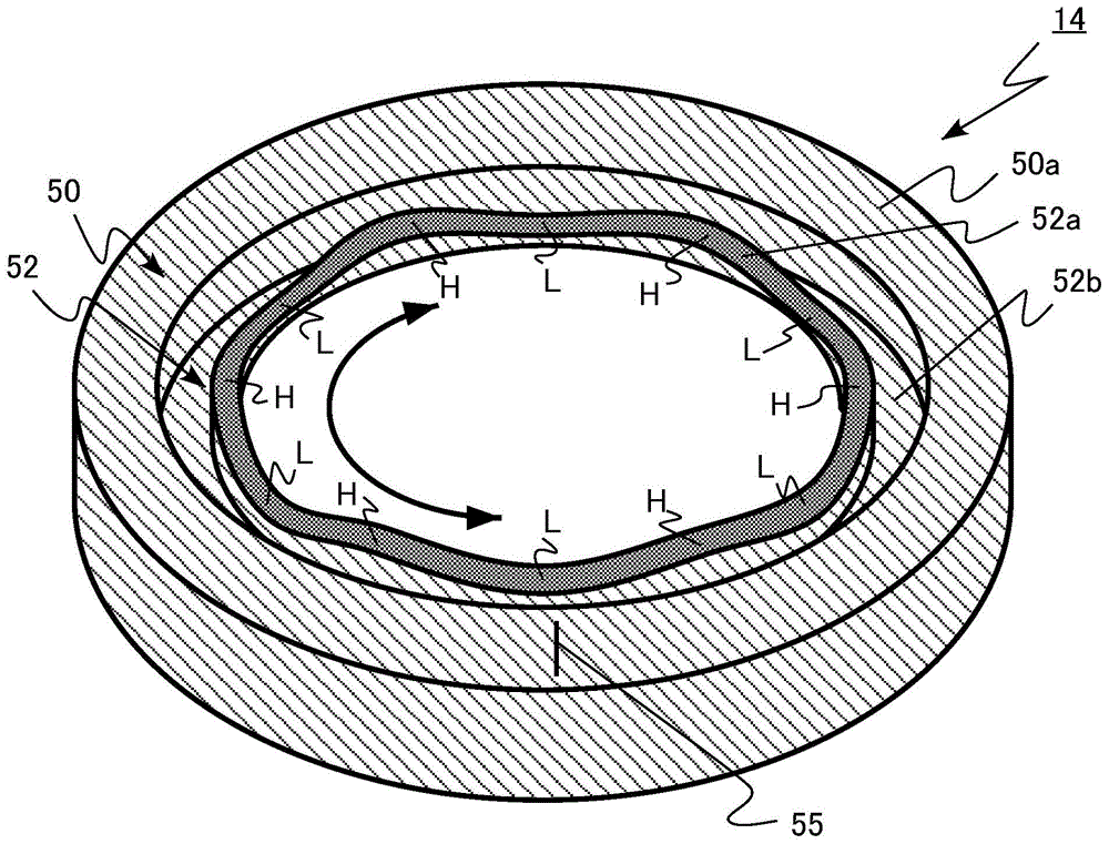
Fig. 2, 3A, and 3B are schematic views of the ring stent of the present embodiment. Fig. 2 is a perspective view, fig. 3A is a plan view, and fig. 3B is a cross-sectional view AA' of fig. 3A.
The annular holder 14 has an annular outer peripheral portion 50 and an annular inner peripheral portion 52. Inner circumferential portion 52 is provided inside outer circumferential portion 50. The outer peripheral portion 50 and the inner peripheral portion 52 are integrally molded, for example.
The inner peripheral portion 52 is a spot facing of the annular holder 14. A wafer W, which is an example of a substrate, is held on the inner peripheral portion 52 and inside the outer peripheral portion 50.
The inner peripheral portion 52 has a substrate mounting surface 52a and a groove 52 b. The substrate mounting surface 52a is annular. The substrate mounting surface 52a is located below the upper surface 50a of the outer peripheral portion 50. The wafer W is placed on the substrate placement surface 52 a.
The substrate mounting surface 52a is a curved surface rotationally symmetric six times that repeats the convex region H and the concave region L in the circumferential direction. In the circumferential direction, the convex regions H and the concave regions L are repeated at a cycle of 60 degrees. That is, if the substrate mounting surface 52a is rotated 60 degrees in the circumferential direction, the shape becomes the same as the shape of the substrate mounting surface 52a before the rotation. The circumferential direction refers to the direction indicated by the double arrow in fig. 2 and 3A.
In fig. 3A, a white circle on the substrate mounting surface 52a is the highest portion of the convex region H, and a black circle is the lowest portion of the concave region L. The height difference between the highest portion and the lowest portion of the substrate mounting surface 52a is, for example, 10 μm or more and 100 μm or less.
The substrate mounting surface 52a has, for example, a sine wave shape.
In the present specification, the term "curved surface" does not exclude the continuation of a fine stepped surface. For example, when the step height difference of the stepped surface is less than or equal to one tenth of the difference between the highest portion and the lowest portion of the substrate mounting surface 52a, the continuation of the stepped surface is also regarded as a curved surface.
The groove 52b is provided between the substrate mounting surface 52a and the outer peripheral portion 50. The groove 52b is annular.
An alignment mark 55 is provided on the upper surface 50a of the outer peripheral portion 50, for example, at a position corresponding to one lowest portion of the substrate mounting surface 52 a. The alignment mark 55 is, for example, a linear groove provided on the upper surface 50 a. The alignment mark may be formed to protrude from a side surface of the outer peripheral portion 50 of the ring holder 14 toward the inner peripheral portion 52. In order to show the crystal orientation, a notch such as a notch or an orientation flat (orientation flat) is usually provided in the wafer W, and the shape of the inward peripheral portion of the alignment mark may be aligned with the shape of the notch.
The alignment mark 55 can be used, for example, as a mark for positional alignment when the ring holder 14 is attached to the rotator unit 16. The mark may be used, for example, as a mark for aligning the position of the wafer W when the wafer W is placed on the ring holder 14. Since the unevenness of the substrate mounting surface 52a is difficult to visually confirm, it is useful to provide the alignment mark 55.
Further, the alignment mark 55 may be provided in a plurality of positions. Further, it may be provided at a position corresponding to the highest portion of the substrate mounting surface 52 a. Further, the substrate mounting surface 52a may be provided at a position corresponding to both the bottommost portion and the topmost portion. Alternatively, the outer peripheral portion 50 may be provided at a position other than the upper surface 50 a.
Next, the vapor phase growth method of the present embodiment will be explained. The vapor phase growth method of the present embodiment uses the epitaxial growth apparatus shown in fig. 1. Fig. 4 is a diagram illustrating a vapor phase growth method according to the present embodiment.
A case will be described as an example in which a laminated film in which a plurality of indium gallium nitride films (InGaN films) and gallium nitride films (GaN films) are alternately laminated is formed on an underlying GaN film. A GaN film and an InGaN film are examples of the nitride semiconductor film. The laminated film is, for example, an MQW (Multi Quantum Well) layer used for a Light-Emitting layer of an LED (Light Emitting Diode).
First, the wafer W is carried into the reaction chamber 10. The wafer W is a silicon substrate having a {111} plane as a surface. The error in the plane orientation of the wafer W is preferably 3 degrees or less, and more preferably 2 degrees or less. In the example of fig. 4, the silicon substrate including the notch N has a diameter direction of [1-10 ]. The thickness of the silicon substrate is, for example, 700 μm or more and 1.2mm or less. The {111} plane represents a plane which is crystallographically equivalent to the (111) plane. Further, fig. 4 shows an example in which a notch is provided to show the crystal axis direction of the substrate, but an orientation flat or the like may be provided for the same purpose.
Next, the wafer W is placed on the substrate placing surface 52a of the ring holder 14. As shown in fig. 4, the wafer W is placed so that the <1-10> direction of the silicon substrate coincides with the direction connecting the opposing concave regions L. More specifically, the wafer W is placed so that the <1-10> direction of the silicon substrate coincides with the direction in which the lowest portions of the recessed regions L, which are diametrically opposed and sandwich the center of the ring holder 14, are connected to each other in the ring holder 14.
For example, the notch N of the wafer W is aligned with the alignment mark 55, and the wafer is placed so that the direction of [1-10] of the silicon substrate coincides with the direction connecting the opposing recessed regions L. Further, the expression of <1-10> direction means a direction which is crystallographically equivalent to the [1-10] direction.
By aligning the notch N of the wafer W with the alignment mark 55, all 3 directions of the directions connecting the opposing concave regions L coincide with the [1-10] direction of the silicon substrate. Even if the [1-10] direction of the silicon substrate does not completely coincide with the direction connecting the opposing concave regions L, it is sufficient that the direction substantially coincides within an error range that can be generated when the wafer W is mounted on the ring holder 14. For example, the angle may be converted so as to be uniform within a range of ± 3 degrees.
Then, the wafer W is heated by the inner heater 24 and the outer heater 26 provided below the ring holder 14 while being rotated by the rotation driving mechanism 20.
Next, buffer layers of AlN (aluminum nitride) and AlGaN (aluminum gallium nitride) were formed on the wafer using TMA, TMG, and ammonia, and then an underlying GaN film was grown. Next, an InGaN film and a GaN film are alternately formed on the underlying GaN film to form a MQW layer.
In the case of forming an InGaN film, a mixed gas of TMG and TMI, for example, with nitrogen as a carrier gas, is supplied from the first gas supply channel 11 to the reaction chamber 10. In addition, for example, ammonia is supplied from the second gas supply channel 12 to the reaction chamber 10. In addition, nitrogen gas, for example, as a diluent gas is supplied from the third gas supply channel 13 to the reaction chamber 10.
In the case of forming a GaN film, for example, TMG with nitrogen gas as a carrier gas is supplied from the first gas supply channel 11 to the reaction chamber 10. In addition, for example, ammonia is supplied from the second gas supply channel 12 to the reaction chamber 10. In addition, nitrogen gas, for example, as a diluent gas is supplied from the third gas supply channel 13 to the reaction chamber 10.
After the MQW layer is formed, the heating of the inner heater 24 and the outer heater 26 is stopped, and the temperature of the wafer W is lowered. Then, the wafer is carried out of the reaction chamber 10.
Next, the operation and effect of the vapor phase growth apparatus, the ring holder, and the vapor phase growth method according to the present embodiment will be described.
The properties of the epitaxial single crystal film formed on the surface of the wafer W, such as the film thickness, chemical composition, and crystallinity, depend on the temperature of the wafer W. Therefore, if the temperature unevenness in the surface of the wafer W becomes large, the film characteristics vary in the surface of the wafer W. Therefore, it is desirable to improve the uniformity of temperature within the wafer plane.
Fig. 5, 6A, 6B, and 7 are diagrams illustrating the operation and effect of the vapor phase growth apparatus according to the present embodiment.
Fig. 5 is a perspective view of a ring holder 15 of a comparative embodiment. The ring holder 15 of the comparative embodiment is different from the ring holder 14 of the present embodiment in that the substrate mounting surface 52a is not a curved surface but a flat surface. The ring holder 15 of the comparative embodiment is different from the ring holder 14 of the present embodiment in that the substrate mounting surface 52a does not have the convex region H and the concave region L in the circumferential direction.
Fig. 6A and 6B are diagrams showing results of the case where the MQW layer was formed using the ring holder 15 of the comparative method in the same manner as in the above-described vapor phase growth method. Fig. 6A is a diagram showing the characteristic distribution in the surface of the wafer W, and fig. 6B is a graph showing the characteristic distribution in the circumferential direction in the outer peripheral region of the wafer W.
The horizontal axis of fig. 6B represents the position in the circumferential direction, and the vertical axis represents the light emission peak wavelength and the wafer height of the MQW layer. The solid line is the peak wavelength of the emission and the dashed line is the wafer height. In addition, the circumferential direction refers to the direction indicated by the arrow in fig. 6A. The wafer height is a height of the wafer surface measured after the MQW-containing layer is formed on the wafer W, and is expressed with reference to the lowest position of the wafer surface.
The emission peak wavelength was determined by the following method: the wafer W is irradiated with excitation light, and the wavelength of fluorescence emitted from the MQW layer is measured. Fig. 6B shows the circumferential direction dependence of the emission peak wavelength in the outer peripheral region of the wafer W.
The emission peak wavelength of the MQW layer depends on the temperature of the wafer W. For example, the higher the temperature of the wafer W at the time of forming the MQW, the shorter the emission peak wavelength. For example, the lower the temperature of the wafer W at the time of forming the MQW, the longer the emission peak wavelength.
Fig. 6B shows an example of the measurement results of the distribution of the emission peak wavelength at the outer peripheral portion and the distribution of the wafer height for the wafer W after the MQW-containing layer is actually grown. As shown in fig. 6B, it is understood that the light emission peak wavelength at the outer peripheral portion of the wafer W is periodically changed, and the change is consistent with the wafer height of the wafer W. Further, as shown in fig. 6B, the regions appear at a period of 60 degrees. In other words, the distribution of the emission peak wavelength in the outer peripheral region of the wafer W is six-fold rotationally symmetric.
If the results and the relationship between the wafer temperature and the emission peak wavelength during the MQW growth are considered together, it can be seen that: as shown in fig. 6A, in the MQW film formation, a region having a short emission peak wavelength, i.e., a region having a high MQW film formation temperature (short wavelength/high temperature in the figure), and a region having a long emission peak wavelength, i.e., a region having a low MQW film formation temperature (long wavelength/low temperature in the figure) alternate in the circumferential direction in the outer peripheral region of the wafer W.
As shown in fig. 6B, the wafer W in the region where the temperature is high during film formation has a low height, and the wafer W in the region where the temperature is low during film formation has a high height. The region where the temperature is high at the time of film formation is a region corresponding to the <1-10> direction of the silicon substrate when viewed from the center of the wafer on the outer peripheral portion of the wafer W.
Even if the wafer W is rotated by 30 degrees in advance and placed on the ring holder 15, the region having a high temperature during film formation coincides with the <1-10> direction of the silicon substrate of the wafer W. Therefore, the temperature distribution generated in the ring-shaped stent 15 is not the cause of the periodic temperature distribution.
The reason why the temperature distribution in the outer peripheral region of the wafer W is generated is considered as follows. That is, in the deposition of the MQW layer, the wafer W is deformed depending on the crystal orientation, and a periodic warp in the circumferential direction occurs in the outer peripheral region of the wafer W. As a result of the wafer W warping, the back surface of the wafer W in the low-height region of the wafer W comes into contact with the substrate mounting surface 52a of the ring holder 15. On the other hand, the back surface of the wafer W in the high-height region of the wafer W is separated from the substrate mounting surface 52a of the ring holder 15 and is not in contact therewith.
During film formation, the wafer W is heated from the back side by the internal heater 24 and the external heater 26. Heat is conducted between the back surface of the wafer W and the ring holder 15 through the substrate mounting surface 52 a.
Therefore, for example, the region of the back surface of the wafer W in contact with the substrate mounting surface 52a becomes high in temperature, and the region not in contact therewith becomes low in temperature. In the example of the present embodiment, the height of the wafer W in the <1-10> direction of the silicon substrate becomes low, and the wafer W comes into contact with the substrate mounting surface 52a and becomes high in temperature. On the other hand, the wafer W in the region deviated from the <1-10> direction by 30 degrees has a high height and is not in contact with the substrate mounting surface 52a, and becomes a low temperature.
As shown in fig. 2 and 3A, the ring holder 14 of the present embodiment includes a substrate mounting surface 52a on which the convex regions H and the concave regions L are repeated at a cycle of 60 degrees in the circumferential direction. By aligning the <1-10> direction of the silicon substrate with the concave region L, the concave-convex shape of the back surface of the wafer W caused by the warpage of the wafer W can be aligned with the concave-convex shape of the substrate mounting surface 52 a. Therefore, the back surface of the wafer W uniformly contacts the substrate mounting surface 52a, and the occurrence of a periodic temperature distribution depending on the crystal orientation in the outer peripheral region of the wafer W is suppressed.
Even if the curved surface shape of the substrate mounting surface 52a and the shape of the back surface of the wafer W cannot be perfectly aligned and a part of the back surface of the wafer W is not in contact with each other, the distance between the substrate mounting surface 52a and the back surface of the wafer W is significantly shorter than in the case of the comparative method. The temperature of the wafer W is also increased by the radiant heat from the substrate mounting surface 52 a. Therefore, even if a part of the back surface of the wafer W is not in contact with the substrate mounting surface 52a, the occurrence of a periodic temperature distribution depending on the crystal orientation in the outer peripheral region of the wafer W can be suppressed.
In the annular stand 14 of the present embodiment, the difference between the highest portion and the lowest portion of the substrate mounting surface 52a is preferably 10 μm or more and 100 μm or less, and more preferably 20 μm or more and 50 μm or less. If the amount is less than the above range, the warpage of the wafer W may not be sufficiently coped with. If the wafer W warps more than the above range, the wafer W may slip.
Fig. 7 is a plan view showing a state where the center of the wafer W is placed off the center of the ring holder 14. For example, in the film formation of the wafer W, the ring holder 14 is rotated with the wafer W placed thereon. At this time, the wafer W may be deviated from the center of the ring holder 14 due to a centrifugal force acting on the wafer W.
For example, in the case where the groove 52b is not provided in the ring holder, if the center of the wafer W is deviated from the center of the ring holder 14, the contact area with the ring holder of the outer periphery of the back surface of the wafer W varies depending on the position. Therefore, temperature unevenness in the outer peripheral region of the wafer W is likely to occur.
The ring holder 14 of the present embodiment is provided with a groove 52b between the substrate mounting surface 52a and the outer peripheral portion 50. Therefore, the back surface of the wafer W is in contact with the ring holder 14 only on the substrate placement surface 52a of the inner peripheral portion 52.
Therefore, as shown in fig. 7, even when the center of the wafer W is placed off the center of the ring holder 14, the contact area between the outer periphery of the back surface of the wafer W and the ring holder 14 does not change depending on the position. Therefore, for example, temperature unevenness in the outer peripheral region of the wafer W is less likely to occur as compared with a ring holder not provided with the groove 52 b.
As described above, according to the vapor phase growth apparatus, the ring holder, and the vapor phase growth method of the present embodiment, the temperature uniformity of the wafer can be improved by reducing the temperature unevenness in the circumferential direction of the outer peripheral region of the wafer W. Therefore, a film with less variation in characteristics can be formed.
(embodiment 2)
The vapor phase growth apparatus and the ring holder according to the present embodiment are the same as those of embodiment 1 except that the inner peripheral portion has a plurality of island-shaped projections projecting inward of the outer peripheral portion. Therefore, description of the contents overlapping with embodiment 1 is omitted.
Fig. 8A and 8B are schematic views of the ring stent of the present embodiment. Fig. 8A is a plan view, and fig. 8B is a BB' sectional view of fig. 8A.
The ring holder 64 of the present embodiment has a plurality of island-shaped projections 52c projecting inward of the outer peripheral portion 50 on the inner peripheral portion 52. For example, island-shaped convex portions 52c protruding in the center direction are provided at 8 positions on the inner peripheral surface of the outer peripheral portion 50. The plurality of island-shaped projections 52c are separated from the substrate mounting surface 52 a.
Fig. 9 is a diagram illustrating the operation and effect of the vapor phase growth apparatus according to the present embodiment. Fig. 9 is a plan view showing a state where the center of the wafer W is placed off the center of the ring holder 64.
The irregularities of the substrate mounting surface 52a are formed on the assumption that the center of the wafer W coincides with the center of the ring holder 64. Therefore, if the wafer W is placed with its center displaced from the center of the ring holder 64, the uneven shape of the back surface of the wafer W caused by the warp of the wafer W cannot be aligned with the uneven shape of the substrate placement surface 52a, and there is a possibility that the temperature unevenness in the circumferential direction of the outer peripheral region of the wafer W becomes large.
For example, as shown in fig. 7, in the case of the ring holder 14 according to embodiment 1, a large deviation occurs between the center of the wafer W and the center of the ring holder 14. Further, the end of the wafer W is in contact with or close to the outer peripheral portion 50 over a wide range, and the temperature of the end of the wafer W increases due to heat conduction from the outer peripheral portion 50, for example. Therefore, the temperature unevenness in the circumferential direction in the outer peripheral region of the wafer W may further increase.
In the case of the ring holder 64 of the present embodiment, the inner peripheral portion 52 has a plurality of island-shaped projections 52c projecting inward of the outer peripheral portion 50. Therefore, as shown in fig. 9, even if the center of the wafer W is displaced from the center of the ring holder 64, the end of the wafer W contacts the island-shaped convex portion 52c, and the displacement between the center of the wafer W and the center of the ring holder 64 can be restricted to be small. Therefore, the deviation between the uneven shape of the back surface of the wafer W and the uneven shape of the substrate mounting surface 52a due to the warpage of the wafer W can be suppressed to be small.
The end of the wafer W and the outer peripheral portion 50 are in contact only with the island-shaped convex portion 52 c. Therefore, the contact area between the end portion of the wafer W and the outer peripheral portion 50 is smaller than that in the case of embodiment 1 shown in fig. 7. This reduces the temperature unevenness in the circumferential direction in the outer peripheral region of the wafer W.
The number of island-shaped projections 52c is not necessarily limited to 8, and may be less than 8, or more than 8. However, when the wafer W is offset from the center of the ring holder 64, the end of the wafer W is preferably kept in contact with the convex portion 52 c. From this viewpoint, the number of island-shaped projections 52c is preferably at least 3.
According to the vapor phase growth apparatus of the present embodiment, the temperature unevenness in the circumferential direction of the outer peripheral region of the wafer W can be further reduced by embodiment 1. Therefore, the temperature uniformity of the wafer can be further improved.
As described above, the embodiments of the present invention have been described with reference to specific examples. The above embodiments are merely examples, and do not limit the present invention. Further, the constituent elements of the respective embodiments may be appropriately combined.
For example, although the embodiment has been described with the case where the annular groove 52b is provided in the inner peripheral portion 52 as an example, the annular groove 52b may not be provided.
In addition, although the embodiment has been described using a single wafer type vapor phase growth apparatus as an example, the present invention is not limited to a single wafer type vapor phase growth apparatus as long as it uses a ring holder, and may be applied to a batch type vapor phase growth apparatus in which a plurality of wafers W are simultaneously deposited.
In the embodiments, the case where a multilayer film in which a plurality of indium gallium nitride films and gallium nitride films are stacked on a GaN film is epitaxially grown was described as an example, but the present invention can also be applied to film formation of a single crystal film of other group III-V nitride-based semiconductor such as aluminum nitride (AlN) or aluminum gallium nitride (AlGaN). The present invention can also be applied to a III-V semiconductor such as GaAs. Further, the present invention can be applied to film formation of other films.
In the embodiment, the case where the process gases are mixed in the shower plate has been described as an example, but the process gases may be mixed before entering the shower plate. The process gas may be in a separated state before being discharged from the shower plate into the reaction chamber.
Further, the outer peripheral portion 50 and the inner peripheral portion 52 of the ring holder 14, 64 are integrally molded, but the inner peripheral portion 52 of the ring holder 14, 64 or a part thereof may be formed in a separable manner. By making the inner peripheral portion 52 or a part thereof separable, for example, ring holders of various shapes can be applied, and fine adjustment of the temperature distribution in the outer peripheral region of the wafer W becomes easy. The ring-shaped holders 14 and 64 may be used in combination with a disk-shaped holder, or may be integrated with a disk-shaped holder.
In the embodiment, the case where two types of the inner heater 24 and the outer heater 26 are provided as the heaters has been described as an example, but only 1 type of the heaters may be provided. In addition, the number of the heaters may be 3 or more.
In the case where the film is formed on the wafer W according to the embodiment described above, the characteristics in the circumferential direction are evaluated, and then the difference in height between the concave portion and the convex portion is further finely adjusted, it is possible to further improve the uniformity of the characteristics in the circumferential direction.
In the embodiments, the description of the device configuration, the manufacturing method, and other parts not directly necessary for the description of the present invention is omitted, but the necessary device configuration, manufacturing method, and other parts may be appropriately selected and used. In addition, all of the vapor phase growth apparatus, the ring holder, and the vapor phase growth method, which have the elements of the present invention and can be appropriately designed and modified by those skilled in the art, are included in the scope of the present invention. The scope of the invention is defined by the scope of the claims and their equivalents.