CN107871760B - Organic light emitting display panel with built-in touch screen and organic light emitting display device - Google Patents
Organic light emitting display panel with built-in touch screen and organic light emitting display device Download PDFInfo
- Publication number
- CN107871760B CN107871760B CN201611233480.1A CN201611233480A CN107871760B CN 107871760 B CN107871760 B CN 107871760B CN 201611233480 A CN201611233480 A CN 201611233480A CN 107871760 B CN107871760 B CN 107871760B
- Authority
- CN
- China
- Prior art keywords
- touch
- light emitting
- organic light
- emitting display
- display panel
- Prior art date
- Legal status (The legal status is an assumption and is not a legal conclusion. Google has not performed a legal analysis and makes no representation as to the accuracy of the status listed.)
- Active
Links
Images


Classifications
-
- H—ELECTRICITY
- H10—SEMICONDUCTOR DEVICES; ELECTRIC SOLID-STATE DEVICES NOT OTHERWISE PROVIDED FOR
- H10K—ORGANIC ELECTRIC SOLID-STATE DEVICES
- H10K59/00—Integrated devices, or assemblies of multiple devices, comprising at least one organic light-emitting element covered by group H10K50/00
- H10K59/40—OLEDs integrated with touch screens
-
- G—PHYSICS
- G06—COMPUTING; CALCULATING OR COUNTING
- G06F—ELECTRIC DIGITAL DATA PROCESSING
- G06F3/00—Input arrangements for transferring data to be processed into a form capable of being handled by the computer; Output arrangements for transferring data from processing unit to output unit, e.g. interface arrangements
- G06F3/01—Input arrangements or combined input and output arrangements for interaction between user and computer
- G06F3/03—Arrangements for converting the position or the displacement of a member into a coded form
- G06F3/041—Digitisers, e.g. for touch screens or touch pads, characterised by the transducing means
- G06F3/0412—Digitisers structurally integrated in a display
-
- G—PHYSICS
- G06—COMPUTING; CALCULATING OR COUNTING
- G06F—ELECTRIC DIGITAL DATA PROCESSING
- G06F3/00—Input arrangements for transferring data to be processed into a form capable of being handled by the computer; Output arrangements for transferring data from processing unit to output unit, e.g. interface arrangements
- G06F3/01—Input arrangements or combined input and output arrangements for interaction between user and computer
- G06F3/03—Arrangements for converting the position or the displacement of a member into a coded form
- G06F3/041—Digitisers, e.g. for touch screens or touch pads, characterised by the transducing means
- G06F3/0416—Control or interface arrangements specially adapted for digitisers
- G06F3/04164—Connections between sensors and controllers, e.g. routing lines between electrodes and connection pads
-
- G—PHYSICS
- G06—COMPUTING; CALCULATING OR COUNTING
- G06F—ELECTRIC DIGITAL DATA PROCESSING
- G06F3/00—Input arrangements for transferring data to be processed into a form capable of being handled by the computer; Output arrangements for transferring data from processing unit to output unit, e.g. interface arrangements
- G06F3/01—Input arrangements or combined input and output arrangements for interaction between user and computer
- G06F3/03—Arrangements for converting the position or the displacement of a member into a coded form
- G06F3/041—Digitisers, e.g. for touch screens or touch pads, characterised by the transducing means
- G06F3/044—Digitisers, e.g. for touch screens or touch pads, characterised by the transducing means by capacitive means
- G06F3/0443—Digitisers, e.g. for touch screens or touch pads, characterised by the transducing means by capacitive means using a single layer of sensing electrodes
-
- H—ELECTRICITY
- H10—SEMICONDUCTOR DEVICES; ELECTRIC SOLID-STATE DEVICES NOT OTHERWISE PROVIDED FOR
- H10K—ORGANIC ELECTRIC SOLID-STATE DEVICES
- H10K50/00—Organic light-emitting devices
- H10K50/80—Constructional details
- H10K50/805—Electrodes
- H10K50/82—Cathodes
- H10K50/828—Transparent cathodes, e.g. comprising thin metal layers
-
- H—ELECTRICITY
- H10—SEMICONDUCTOR DEVICES; ELECTRIC SOLID-STATE DEVICES NOT OTHERWISE PROVIDED FOR
- H10K—ORGANIC ELECTRIC SOLID-STATE DEVICES
- H10K50/00—Organic light-emitting devices
- H10K50/80—Constructional details
- H10K50/84—Passivation; Containers; Encapsulations
-
- H—ELECTRICITY
- H10—SEMICONDUCTOR DEVICES; ELECTRIC SOLID-STATE DEVICES NOT OTHERWISE PROVIDED FOR
- H10K—ORGANIC ELECTRIC SOLID-STATE DEVICES
- H10K50/00—Organic light-emitting devices
- H10K50/80—Constructional details
- H10K50/84—Passivation; Containers; Encapsulations
- H10K50/844—Encapsulations
-
- H—ELECTRICITY
- H10—SEMICONDUCTOR DEVICES; ELECTRIC SOLID-STATE DEVICES NOT OTHERWISE PROVIDED FOR
- H10K—ORGANIC ELECTRIC SOLID-STATE DEVICES
- H10K50/00—Organic light-emitting devices
- H10K50/80—Constructional details
- H10K50/86—Arrangements for improving contrast, e.g. preventing reflection of ambient light
- H10K50/865—Arrangements for improving contrast, e.g. preventing reflection of ambient light comprising light absorbing layers, e.g. light-blocking layers
-
- H—ELECTRICITY
- H10—SEMICONDUCTOR DEVICES; ELECTRIC SOLID-STATE DEVICES NOT OTHERWISE PROVIDED FOR
- H10K—ORGANIC ELECTRIC SOLID-STATE DEVICES
- H10K59/00—Integrated devices, or assemblies of multiple devices, comprising at least one organic light-emitting element covered by group H10K50/00
- H10K59/30—Devices specially adapted for multicolour light emission
- H10K59/38—Devices specially adapted for multicolour light emission comprising colour filters or colour changing media [CCM]
-
- G—PHYSICS
- G06—COMPUTING; CALCULATING OR COUNTING
- G06F—ELECTRIC DIGITAL DATA PROCESSING
- G06F2203/00—Indexing scheme relating to G06F3/00 - G06F3/048
- G06F2203/041—Indexing scheme relating to G06F3/041 - G06F3/045
- G06F2203/04111—Cross over in capacitive digitiser, i.e. details of structures for connecting electrodes of the sensing pattern where the connections cross each other, e.g. bridge structures comprising an insulating layer, or vias through substrate
-
- G—PHYSICS
- G06—COMPUTING; CALCULATING OR COUNTING
- G06F—ELECTRIC DIGITAL DATA PROCESSING
- G06F2203/00—Indexing scheme relating to G06F3/00 - G06F3/048
- G06F2203/041—Indexing scheme relating to G06F3/041 - G06F3/045
- G06F2203/04112—Electrode mesh in capacitive digitiser: electrode for touch sensing is formed of a mesh of very fine, normally metallic, interconnected lines that are almost invisible to see. This provides a quite large but transparent electrode surface, without need for ITO or similar transparent conductive material
Abstract
An organic light emitting display panel and an organic light emitting display device having a built-in touch screen. The organic light emitting display panel includes a plurality of sub-pixels defined by a plurality of data lines and a plurality of gate lines in the organic light emitting display panel, an encapsulation layer having an encapsulation function, and a color filter layer on the encapsulation layer. The organic light emitting display device includes the organic light emitting display panel. Both of the organic light emitting display panel with a built-in touch screen and the organic light emitting display device with a built-in touch screen are provided with a structure in which the touch screen can be disposed.
Description
Technical Field
The present disclosure relates to an organic light emitting display panel and an organic light emitting display device having a built-in touch screen.
Background
In response to the development of the information society, there is an increasing demand for various display devices for displaying images. In this regard, a series of display devices such as a Liquid Crystal Display (LCD) device, a Plasma Display Panel (PDP), and an organic light emitting display device have recently come into wide use.
Many display devices provide a touch-based user interface that enables a user to intuitively and conveniently input data or instructions directly into the device, rather than using a conventional data input system such as a key, keyboard, or mouse.
To provide such a touch-based user interface, the ability to sense a touch made by a user and accurately detect touch coordinates is required.
In this regard, the related art enables touch sensing using one touch sensing method selected from various touch sensing methods such as touch sensing using a resistive film, capacitive touch sensing, electromagnetic induction touch sensing, Infrared (IR) touch sensing, and ultrasonic wave touch sensing.
In this regard, capacitive touch sensing is generally used to sense touch and touch coordinates using a plurality of touch electrodes provided on a touch panel as touch sensors based on a change in capacitance between the touch electrodes or between the touch electrodes and a pointer (pointer), such as a hand.
A series of attempts have been made to provide a touch screen panel including electrodes in a display panel to facilitate manufacturing the display device and to reduce the size of the display device.
Among various display apparatuses, since an organic Electroluminescent (EL) device or an Organic Light Emitting Diode (OLED) capable of emitting light by itself is used in the display apparatuses and a separate light source is not required, the organic light emitting display apparatuses can be manufactured to be relatively light and thin.
In addition, organic light emitting display devices are advantageous not only in terms of power consumption since they are driven at low voltages, but also in desirable qualities such as the ability to realize light of a range of colors, fast response speed, wide viewing angle, and high contrast. Accordingly, organic light emitting display devices for next generation displays have been actively studied.
Although the organic light emitting display device is significantly advantageous in terms of display, there are significant difficulties and a series of limitations in terms of a touch screen panel to be provided within the organic light emitting display device.
For example, an encapsulation layer or the like for protecting the organic light emitting display panel from moisture, air, physical impact, or impurities to be generated during a manufacturing process must be provided on the front surface of the organic light emitting display panel in order to make the organic light emitting display panel reliable. However, this therefore results in a relatively complex and difficult process. In addition, the encapsulation layer makes it difficult to determine the position of the touch sensor capable of normally performing touch sensing without degrading display performance.
In addition, in the manufacturing process of the organic light emitting display panel, the organic material limits the degree of freedom of a high temperature process of manufacturing the touch sensor formed of a metal material within the organic light emitting display panel.
It is difficult to provide a touch electrode serving as a touch sensor in an organic light emitting display panel due to limitations of the organic light emitting display panel with respect to structural characteristics and processes. That is, it is considerably difficult to implement an organic light emitting display panel having a built-in touch screen panel.
Accordingly, in the related art organic light emitting display device, a touch structure has been implemented by attaching a touch screen panel to an organic light emitting display panel instead of providing the touch screen panel within the organic light emitting display panel.
In this case, the touch screen panel must be manufactured separately from the organic light emitting display panel before being attached to the organic light emitting display panel, thus resulting in a relatively complicated manufacturing process and increasing the thickness of the resulting organic light emitting display device, both of which are problematic.
Disclosure of Invention
Aspects of the present disclosure provide an organic light emitting display panel with a built-in touch screen and an organic light emitting display device with a built-in touch screen, each of which has a structure in which a touch screen can be disposed.
An organic light emitting display panel with a built-in touch screen and an organic light emitting display device with a built-in touch screen, both of which can improve touch sensing performance, are also provided.
Also provided are an organic light emitting display panel with a built-in touch screen and an organic light emitting display device with a built-in touch screen, both having a structure that can be designed to be slim-profiled.
An organic light emitting display panel with a built-in touch screen and an organic light emitting display device with a built-in touch screen are also provided, both having a touch screen panel disposed therein without affecting display performance.
An organic light emitting display panel with a built-in touch screen and an organic light emitting display device with a built-in touch screen are also provided, each configured such that two types of touch sensor metals (i.e., touch electrodes and touch lines) enabling self-capacitance based touch sensing are disposed in different layers.
According to an aspect of the present disclosure, there is provided an organic light emitting display panel having a built-in touch screen.
The organic light emitting display panel may include: a plurality of sub-pixels defined in the organic light emitting display panel by a plurality of data lines and a plurality of gate lines; and a touch sensor (such as a touch electrode) built in the organic light emitting display panel.
According to another aspect of the present disclosure, an organic light emitting display device having a built-in touch screen may include an organic light emitting display panel having a built-in touch screen.
The organic light emitting display device may further include: a touch sensing circuit for providing a touch driving signal to at least one touch electrode among the plurality of touch electrodes and sensing at least one of a touch and a touch position based on a signal detected using each of the plurality of touch electrodes to which the touch driving signal is applied.
The organic light emitting display panel may further include an encapsulation layer and a color filter layer on the encapsulation layer.
In the organic light emitting display panel, a plurality of touch electrodes corresponding to a touch sensor metal may be on the encapsulation layer.
In the organic light emitting display panel, a plurality of touch lines may be positioned on the encapsulation layer to electrically connect the plurality of touch electrodes to a touch sensing circuit, the plurality of touch lines serving as a touch sensor metal.
In the organic light emitting display panel, the plurality of touch electrodes and the plurality of touch lines may be disposed in different layers sandwiching an insulating layer.
Each of the plurality of touch lines is electrically connected to a corresponding touch electrode of the plurality of touch electrodes through the contact hole and is electrically isolated from the remaining touch electrodes.
In the organic light emitting display panel, each of the plurality of touch lines may overlap at least one of the plurality of touch electrodes.
In the organic light emitting display panel, the plurality of touch electrodes may be disposed between the encapsulation layer and the color filter layer.
In this case, an overcoat layer (overcoat layer) may be disposed between the encapsulation layer and the color filter layer. The plurality of touch electrodes may be disposed between the encapsulation layer and the cover layer.
In the organic light emitting display panel, the plurality of touch electrodes may be disposed on the color filter layer.
In this case, an overcoat layer may be disposed on the color filter layer. The plurality of touch electrodes may be disposed on the cover layer.
According to still another aspect of the present disclosure, an organic light emitting display panel with a built-in touch screen may include: a plurality of sub-pixels defined in the organic light emitting display panel by a plurality of data lines and a plurality of gate lines; and a touch sensor disposed in the organic light emitting display panel.
In the organic light emitting display panel, each of the plurality of sub-pixels may include: an organic light emitting diode including a first electrode, an organic light emitting layer, and a second electrode; a driving transistor for driving the organic light emitting diode; a first transistor electrically connected between a first node of the driving transistor and a data line corresponding to the first transistor among the plurality of data lines; and a storage capacitor connected between the first node and the second node of the driving transistor.
The organic light emitting display panel may further include: an encapsulation layer on the second electrode of the organic light emitting diode; and a color filter layer on the encapsulation layer.
In the organic light emitting display panel, a plurality of touch electrodes may be positioned on the encapsulation layer.
A touch driving signal may be provided to at least one touch electrode among the plurality of touch electrodes. The touch electrode to which the touch driving signal is applied may form a capacitance together with a pointer corresponding to a touch manipulation manner of a user.
The touch or touch position can be sensed using the capacitance formed as described above.
According to the present disclosure set forth above, an organic light emitting display panel with a built-in touch screen and an organic light emitting display device with a built-in touch screen are provided with a structure in which a touch screen panel can be disposed.
In addition, according to the present disclosure, the organic light emitting display panel having the built-in touch screen and the organic light emitting display device having the built-in touch screen can improve touch sensing performance.
In addition, according to the present disclosure, an organic light emitting display panel with a built-in touch screen and an organic light emitting display device with a built-in touch screen are provided with a structure that can be designed to be slim in appearance.
In addition, according to the present disclosure, an organic light emitting display panel with a built-in touch screen and an organic light emitting display device with a built-in touch screen are provided with a touch screen panel disposed therein without affecting display performance.
In addition, according to the present disclosure, an organic light emitting display panel with a built-in touch screen and an organic light emitting display device with a built-in touch screen are provided with a structure in which two types of touch sensor metals (i.e., touch electrodes and touch lines) capable of implementing self-capacitance based touch sensing are disposed in different layers.
Drawings
The above and other objects, features and advantages of the present disclosure will be more clearly understood from the following detailed description taken in conjunction with the accompanying drawings, in which:
fig. 1 is a schematic view illustrating a configuration of an organic light emitting display device having a built-in touch screen according to an exemplary embodiment;
fig. 2 is a schematic circuit diagram illustrating a sub-pixel structure of an organic light emitting display panel having a built-in touch screen according to an exemplary embodiment;
fig. 3 is a schematic circuit diagram illustrating another sub-pixel structure of an organic light emitting display panel having a built-in touch screen according to an exemplary embodiment;
fig. 4 is a schematic view illustrating a display driving pattern in an organic light emitting display panel having a built-in touch screen according to an exemplary embodiment;
fig. 5 is a schematic view illustrating a touch sensing pattern in an organic light emitting display panel having a built-in touch screen according to an exemplary embodiment;
fig. 6 is a schematic view illustrating a single touch electrode in an organic light emitting display panel having a built-in touch screen according to an exemplary embodiment;
fig. 7 is a schematic view illustrating a block-type (bulk-type) touch electrode in an organic light emitting display panel having a built-in touch screen according to an exemplary embodiment;
fig. 8 and 9 are schematic views illustrating a mesh-type touch electrode in an organic light emitting display panel having a built-in touch screen according to an exemplary embodiment;
fig. 10 is a sectional view illustrating an organic light emitting display panel having a built-in touch screen according to an exemplary embodiment;
fig. 11 is a schematic view illustrating a COE structure of an organic light emitting display panel with a built-in touch screen according to an exemplary embodiment;
fig. 12 is a schematic view illustrating a TOE structure of an organic light emitting display panel having a built-in touch screen according to an exemplary embodiment;
fig. 13 is a schematic view illustrating an M-TOE structure of an organic light emitting display panel having a built-in touch screen according to an exemplary embodiment;
fig. 14 and 15 are plan views illustrating an organic light emitting display panel having a built-in touch screen and an M-TOE structure according to an exemplary embodiment;
fig. 16 is a schematic view illustrating a combined structure of a first COE and an M-TOE in an organic light emitting display panel having a built-in touch screen according to an exemplary embodiment;
fig. 17 is a sectional view illustrating a combined structure of a first COE and an M-TOE in an organic light emitting display panel with a built-in touch screen according to an exemplary embodiment;
fig. 18 is a schematic view illustrating a process of manufacturing a first COE and M-TOE combined structure in an organic light emitting display panel with a built-in touch screen according to an exemplary embodiment;
fig. 19 is a schematic view illustrating a combined structure of a second COE and an M-TOE in an organic light emitting display panel with a built-in touch screen according to an exemplary embodiment;
fig. 20 is a sectional view illustrating a second COE and M-TOE combined structure in an organic light emitting display panel with a built-in touch screen according to an exemplary embodiment;
fig. 21 is a schematic view illustrating a process of manufacturing a second COE and M-TOE combined structure in an organic light emitting display panel with a built-in touch screen according to an exemplary embodiment;
fig. 22 is a schematic view illustrating a distance defined between a touch electrode and a second electrode and a parasitic capacitance component formed between the touch electrode and the second electrode in an organic light emitting display panel having a built-in touch screen according to an exemplary embodiment;
fig. 23 is a schematic view illustrating a distance between a touch electrode TE and a second electrode in an organic light emitting display panel having a built-in touch screen and a combined structure of a first COE and an M-TOE;
fig. 24 is a schematic view illustrating a distance between a touch electrode and a second electrode in an organic light emitting display panel having a built-in touch screen and a second COE and M-TOE combined structure;
fig. 25 is a graph illustrating an RC delay and a touch sensing performance according to a distance between a touch electrode and a second electrode in an organic light emitting display panel having a built-in touch screen according to an exemplary embodiment; and
fig. 26 is a schematic view illustrating a no-load driving (load-free driving) for removing a parasitic capacitance component from an organic light emitting display panel having a built-in touch screen according to an exemplary embodiment.
Detailed Description
Reference will now be made in detail to embodiments of the present disclosure, examples of which are illustrated in the accompanying drawings. Throughout this document, reference should be made to the drawings, in which the same reference numerals and symbols will be used to refer to the same or similar components. In the following description of the present disclosure, in the case where known functions and components included herein may make the subject matter of the present disclosure unclear, a detailed description thereof will be omitted.
It will also be understood that, although terms such as "first," "second," "a," "B," "a," and "(B)" may be used herein to describe various elements, these terms are only used to distinguish one element from another. The nature, order, sequence or number of such elements is not limited by these terms. It will be understood that when an element is referred to as being "connected to" or "coupled to" another element, it can be not only "directly connected or coupled to" the other element, but also indirectly connected or coupled to "the other element via" intermediate "elements. In the same context, it will be understood that, when an element is referred to as being formed "on" or "under" another element, the element may be formed not only directly on or under the other element but also indirectly on or under the other element via an intermediate element.
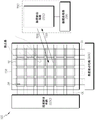
Fig. 1 is a schematic view illustrating a configuration of an organic light emitting display device 100 having a built-in touch screen according to an exemplary embodiment.
Referring to fig. 1, an organic light emitting display device 100 having a built-in touch screen according to an exemplary embodiment can perform a display function of displaying an image and a touch sensing function of a touch made using a pointer such as a finger or a stylus pen.
The organic light emitting display device 100 with a built-in touch screen according to an exemplary embodiment may operate in a touch mode to perform a touch sensing function in a touch mode section (section) and simultaneously operate in a display mode to perform a display function in a display mode section.
The display mode section and the touch mode section may be divided based on time, may be simultaneously located within the same time period, or may overlap based on time.
That is, the display mode operation for displaying an image and the touch mode operation for performing touch sensing can be performed separately or simultaneously.
In order to perform both functions (i.e., a display function and a touch sensing function), the organic light emitting display device 100 with a built-in touch screen according to an exemplary embodiment includes an organic light emitting display panel 110 with a built-in touch screen, a display driving circuit, and a touch sensing circuit TSC. On the organic light emitting display panel 110 having a built-in touch screen, a plurality of sub-pixels SP defined by a plurality of data lines DL and a plurality of gate lines GL are arranged, and a plurality of touch electrodes TE are disposed. The display driving circuit drives the organic light emitting display panel 110 having a built-in touch screen to perform a display function. The touch sensing circuit TSC drives the organic light emitting display panel 110 having a built-in touch screen to perform a touch sensing function.
Referring to fig. 1, the display driving circuit includes a data driving circuit DDC for driving a plurality of data lines DL in a display mode section and a gate driving circuit GDC for driving a plurality of gate lines GL in the display mode section.
The display driver circuit may further include at least one controller to control operation timings of the data driver circuit DDC and the gate driver circuit GDC, supply power to the data driver circuit DDC and the gate driver circuit GDC, and the like.
Referring to fig. 1, in the touch mode section, the touch sensing circuit TSC can provide a touch driving signal TDS to at least one touch electrode among a plurality of touch electrodes TE, and determine an occurrence of a touch and/or a touch position based on a touch sensing signal TSS detected by the touch electrode TE applied with the touch driving signal TDS.
The touch sensing circuit TSC includes a touch driving circuit TDC, a touch processor TP, and the like. The touch driving circuit TDC drives the plurality of touch electrodes TE while the touch processor TP determines the occurrence of a touch and/or a touch position based on signals received from the touch electrodes TE applied with the touch driving signal TDS.
The touch driving circuit TDC can supply the touch driving signal TDS to the plurality of touch electrodes TE to drive the plurality of touch electrodes TE.
In addition, the touch driving circuit TDC can receive the touch sensing signal TSS from the touch electrode TE applied with the touch driving signal TDS.
The touch driving circuit TDC provides the touch processor TP with the received touch sensing signal TSS or sensing data obtained by processing the received touch sensing signal TSS.
The touch processor TP can perform a touch algorithm using the touch sensing signal TSS or the sensing data and determine the occurrence of a touch and/or a touch position by performing the touch algorithm.
As described above, the organic light emitting display device 100 with a built-in touch screen according to an exemplary embodiment uses a self-capacitance-based touch sensing method of determining the occurrence of a touch and/or a touch position by detecting a change in self-capacitance between each touch electrode TE and a pointer.
In the organic light emitting display device 100 with a built-in touch screen according to an exemplary embodiment, the touch driving signal TDS is applied to the touch electrode TE, and the touch sensing signal TSS is detected using the touch electrode TE.
Since the organic light emitting display device with built-in touch screen 100 according to an exemplary embodiment senses a touch using the self-capacitance based touch sensing method described above, the organic light emitting display panel with built-in touch screen 110 only needs to have a self-capacitance based touch sensing structure.
Accordingly, it is not necessary to provide two types of touch sensor electrodes (i.e., a driving electrode and a receiving electrode) to the organic light emitting display panel 110 with a built-in touch screen, and thus a panel manufacturing process is simplified and facilitated to form a touch sensing structure on the organic light emitting display panel 110 with a built-in touch screen.
The data driving circuit DDC, the gate driving circuit GDC, the touch driving circuit TDC, and the touch processor TP are classified according to functions. The source driving circuit SDC, the gate driving circuit GDC, the touch driving circuit TDC, and the touch processor TP may be provided independently of each other, or alternatively, two or more thereof may be integrated with each other.
Fig. 2 is a schematic circuit diagram illustrating one sub-pixel structure of the organic light emitting display panel 110 with a built-in touch screen according to an exemplary embodiment, and fig. 3 is a schematic circuit diagram illustrating another sub-pixel structure of the organic light emitting display panel 110 with a built-in touch screen according to an exemplary embodiment.
Referring to fig. 2, in the organic light emitting display panel 110 having a built-in touch screen according to an exemplary embodiment, each sub-pixel SP mainly includes: an Organic Light Emitting Diode (OLED); a driving transistor DRT for driving the OLED; a first transistor T1 for transmitting data to a first node N1 of the driving transistor DRT corresponding to the gate node; and a storage capacitor C1 for holding the data voltage VDATA corresponding to the image signal voltage or the voltage corresponding to the data voltage during a period of a single frame.
The OLED includes a first electrode (i.e., an anode or a cathode) E1, an organic light emitting layer EL, and a second electrode (i.e., a cathode or an anode) E2.
For example, a base voltage EVSS is applied to the second electrode E2 of the OLED.
The driving transistor DRT drives the OLED by supplying a driving current to the OLED.
The driving transistor DRT has a first node N1, a second node N2, and a third node N3.
The first node N1 of the driving transistor DRT corresponding to the gate node is electrically connected to the source or drain node of the first transistor T1.
The second node N2 of the driving transistor DRT is electrically connected to the first electrode E1 of the OLED, and may be a source node or a drain node.
The third node N3 of the driving transistor DRT is a node to which the driving voltage EVDD is applied, the third node N3 is electrically connected to the driving voltage line DVL through which the driving voltage EVDD is supplied, and the third node N3 is a drain node or a source node.
The driving transistor DRT and the first transistor TI may be embodied as n-type transistors or p-type transistors.
The first transistor T1 is electrically connected between the data line DL and the first node N1 of the driving transistor DRT, and controls the first transistor T1 by a SCAN signal SCAN applied to a gate node of the first transistor T1 through a gate line.
The first transistor T1 is turned on by the SCAN signal SCAN to transmit the data voltage VDATA supplied through the data line DL to the first node of the driving transistor.
The storage capacitor C1 is electrically connected between the first node N1 and the second node N2 of the driving transistor DRT.
The storage capacitor C1 is an external capacitor intentionally designed to be disposed outside the driving transistor DRT, and is not a parasitic capacitor Cgs or Cgd, that is, an internal capacitor existing between the first node N1 and the second node N2 of the driving transistor DRT.
Referring to fig. 3, each pixel SP disposed on the organic light emitting display panel according to the exemplary embodiment includes a second transistor T2 in addition to an OLED, a driving transistor DRT, a first transistor T1, and a storage capacitor C1.
Referring to fig. 3, the second transistor T2 is electrically connected between the second node N2 of the driving transistor DRT and a reference voltage line RVL through which a reference voltage VREF is supplied, and the second transistor T2 is controlled by a sensing signal SENSE (a kind of scan signal) supplied to a gate node of the second transistor T2.
Since the second transistor T2 is also provided, the voltage state of the second node N2 of the driving transistor DRT of the sub-pixel SP can be more effectively controlled.
The second transistor T2 is turned on by the sensing signal SENSE to apply the reference voltage VREF supplied through the reference voltage line RVL to the second node N2 of the driving transistor DRT.
The sub-pixel structure illustrated in fig. 3 facilitates accurately initializing the voltage of the second node N2 of the driving transistor DRT and sensing unique characteristics (e.g., threshold voltage or mobility) of the driving transistor DRT and unique characteristics (e.g., threshold voltage) of the OLED.
The SCAN signal SCAN and the SENSE signal SENSE may be separate gate signals. In this case, the SCAN signal SCAN and the sensing signal SENSE may be applied to the gate node of the first transistor T1 and the gate node of the second transistor T2 through different gate lines, respectively.
Alternatively, the SCAN signal SCAN and the SENSE signal SENSE may be the same signal. In this case, the SCAN signal SCAN and the SENSE signal SENSE may be commonly applied to the gate node of the first transistor T1 and the gate node of the second transistor T2.
Hereinafter, a touch screen built-in structure enabling a touch screen to be built in an organic light emitting display panel, which can have the above-described sub-pixel structure, and an integrated driving method, an integrated driving circuit, and a signal connection structure related to the touch screen built-in structure will be described.
In the organic light emitting display panel 110 with a built-in touch screen, when the sub-pixel structure includes the first electrode E1, the organic light emitting layer EL disposed on the first electrode E1, and the second electrode E2 disposed on the organic light emitting layer EL, an encapsulation layer may be disposed on the second electrode E2 to prevent moisture, air, and the like from penetrating thereinto.
Fig. 4 is a schematic view illustrating a display driving pattern in the organic light emitting display panel 110 having a built-in touch screen according to an exemplary embodiment.
Referring to fig. 4, each subpixel SP may have the subpixel structure illustrated in fig. 2 or 3, and in a display mode section, may be driven by a single data line DL and one or more gate lines GL.
The data pad DP is connected to an end portion of the data line DL to electrically connect the data line DL to the data driving circuit DDC.
Referring to fig. 4, although the size of the single touch electrode TE may be the same as that of the single subpixel SP, the size of the single touch electrode TE may be larger than that of the single subpixel SP in terms of the degree of efficiency of touch driving and touch sensing.
Fig. 5 is a schematic view illustrating a touch driving pattern in the organic light emitting display panel 110 having a built-in touch screen according to an exemplary embodiment.
Referring to fig. 5, a touch sensing pattern (or touch sensor metal) including a plurality of touch electrodes TE, a plurality of touch lines TL, and a plurality of touch pads TP is disposed on the organic light emitting display panel 110 having a built-in touch screen according to an exemplary embodiment.
Since the plurality of touch electrodes TE are touch sensors for self-capacitance-based touch sensing, the respective touch electrodes TE function as both driving electrodes and receiving electrodes (i.e., sensing electrodes).
In this regard, the plurality of touch electrodes TE are electrically isolated from each other, respectively.
In addition, the plurality of touch electrodes TE do not overlap each other.
The plurality of touch lines TL are signal lines for electrically connecting the plurality of touch electrodes TE to the touch sensing circuit TSC.
A plurality of touch pads TP are disposed on predetermined ends of the plurality of touch lines TL and are electrically connected to the touch sensing circuit TSC.
Fig. 6 is a schematic view illustrating a single touch electrode among a plurality of touch electrodes TE in the organic light emitting display panel 110 with a built-in touch screen according to an exemplary embodiment.
Referring to fig. 6, a single touch electrode TE has a touch driving signal TDS provided through a single touch line TL.
The single subpixel SP operates using a data voltage VDATA supplied through the single data line DL and a scan signal supplied through one or more gate lines GL according to the structure of the subpixel.
As illustrated in fig. 6, the size of each of the plurality of touch electrodes TE is larger than the size of each of the plurality of sub-pixels SP.
For example, the size of a single touch electrode TE may be larger than the size of two sub-pixels SP.
Since the size of the single touch electrode TE is larger than the size of the two sub-pixels SP as described above, two or more gate lines GL or two or more data lines DL may be disposed in an area occupied by each touch electrode TE.
Since the size of the single touch electrode TE is larger than the size of the two sub-pixels SP in the organic light emitting display panel 110 with a built-in touch screen as described above, the number of the plurality of touch electrodes can be reduced. Accordingly, the number of touch driving entities, to which the touch driving signals TDS are supplied to the touch electrodes TE, may be reduced or sensing data may be reduced, and thus, the efficiency of touch sensing may be improved.
However, when the number of the plurality of touch electrodes is reduced due to an increase in the size of the touch electrodes, the efficiency of touch sensing may be improved due to the reduced sensing data, but the accuracy of touch sensing may be reduced.
Therefore, the number and size of the touch electrodes must be accurately set in consideration of the efficiency and accuracy of touch sensing.
In the touch mode section, the touch driving signal TDS supplied to one or more touch electrodes or all touch electrodes TE among the touch electrodes TE may be a pulse-type signal.
The touch drive signal TDS may be a pulse-type signal having a waveform (e.g., a spherical wave, a sine wave, or a triangular wave).
The touch driving signal TDS may have a predetermined wavelength, phase, amplitude, etc.
Fig. 7 is a schematic view illustrating a block-type touch electrode TE in an organic light emitting display panel 110 having a built-in touch screen according to an exemplary embodiment.
Referring to fig. 7, each of the plurality of touch electrodes TE may be a block type touch electrode without an open area (OA in fig. 8).
When the touch electrode TE is a block type touch electrode, the touch electrode TE may be a transparent electrode.
When the touch electrode TE is formed as a block type touch electrode without the opening area OA as described above, the touch electrode TE can be easily patterned.
In addition, when the touch electrode TE is embodied as a transparent electrode, the touch electrode TE having no influence on light emission performance in the sub pixel region can be formed on the organic light emitting display panel 110 having a built-in touch screen.
Fig. 8 and 9 are schematic views illustrating a mesh type touch electrode TE in an organic light emitting display panel 100 with a built-in touch screen according to an exemplary embodiment.
As illustrated in fig. 8 and 9, each of the plurality of touch electrodes TE may be a mesh-type touch electrode having an opening area OA.
When the touch electrode TE is a mesh type touch electrode, the touch electrode TE may be a transparent or opaque electrode.
When the touch electrode TE is embodied as a mesh-type touch electrode, each opening area PA corresponds to a light emitting area of each sub-pixel. That is, the first electrode E1 of each sub-pixel is positioned in each opening area OA.
As illustrated in fig. 8, the mesh-type touch electrode TE or the opening area OA thereof may have a diamond shape according to the arrangement shape of the sub-pixels.
Alternatively, as illustrated in fig. 9, the mesh-type touch electrode TE or the opening area OA thereof may have a rectangular shape according to the arrangement shape of the sub-pixels.
The mesh-type touch electrode TE or the opening area OA thereof may have various shapes, instead of a diamond shape or a rectangular shape, according to the shape of the sub-pixel.
As described above, the touch electrode TE suitable for the structure and shape of the sub-pixel without reducing the light emitting efficiency of the sub-pixel can be formed on the organic light emitting display panel 110 having the built-in touch screen.
Fig. 10 is a sectional view illustrating an organic light emitting display panel 110 having a built-in touch screen according to an exemplary embodiment.
A cross-sectional structure of the organic light emitting display panel 110 having a built-in touch screen will be described with reference to fig. 10.
A Polyimide (PI) layer L02 is located on the substrate or backplate L01.
A buffer layer L03 is located on the polyimide layer L02, and an interlayer insulating film L04 is located on the buffer layer L03.
The gate layer L05 is located on the interlayer insulating film L04, and a gate or the like can be formed in a desired position on the gate layer L05.
The gate insulating film L06 is located on the gate layer L05.
The source/drain layer L07 is located on the gate insulating film L06.
Signal lines such as data lines DL and link lines GL and source/drain electrodes of various transistors may be formed on the source/drain layer L07.
The protective layer L08 is located on the source/drain layer L07.
The planarization layer L09 was located on the protective layer L08, and the first electrode layer L10 was located on the planarization layer L09. The first electrode layer L10 has a first electrode E1 formed in the light emitting portion of the sub-pixel.
A bank layer L11 is positioned on the first electrode layer L10, and an organic light emitting layer L12 is positioned on the bank layer L11.
The second electrode layer L13 is positioned on the organic light emitting layer L12. The second electrode layer L13 is formed in common in all the sub-pixel regions.
An encapsulation layer L14 for preventing moisture, air, etc. from penetrating is located on the second electrode layer L13.
A dam (dam) may be provided on the peripheral portion of the panel, the dam being stacked higher than the peripheral portion to prevent the encapsulation layer L14 from collapsing.
The encapsulation layer L14 may be a single layer, or may be composed of two or more layers stacked on each other.
In addition, the encapsulation layer L14 may be a metal layer, or may have a multi-layer structure in which two or more layers composed of an organic layer and an inorganic layer are stacked on each other.
In the implementation illustrated in fig. 10, the encapsulation layer L14 is a multilayer structure composed of a first encapsulation layer L14a, a second encapsulation layer L14b, and a third encapsulation layer L14 c.
Each of the first encapsulation layer L14a, the second encapsulation layer L14b, and the third encapsulation layer L14c may be an organic layer and/or an inorganic layer.
Referring to fig. 10, the thickness of the encapsulation layer L14 may be determined in consideration of encapsulation performance.
The thickness of the encapsulation layer L14 may have an effect on RC delay and touch sensing performance (touch sensitivity) with respect to touch driving and touch sensing.
Therefore, the thickness of the encapsulation layer L14 must be determined in consideration of RC delay and touch sensing performance (touch sensitivity).
This feature will be described in more detail with reference to fig. 22 to 25.
In addition, the organic light emitting display panel 110 with a built-in touch screen according to an exemplary embodiment has a color filter on package (COE) structure in which a color filter layer is positioned on the package layer L14 and a touch sensor on package layer (TOE) structure in which touch sensor metal such as a touch electrode TE and a touch line TL is positioned on the package layer L14.
Hereinafter, the COE structure and the TOE structure will be described in more detail.
Fig. 11 is a schematic view illustrating a COE structure of an organic light emitting display panel 110 with a built-in touch screen according to an exemplary embodiment.
Referring to fig. 11, the organic light emitting display panel 110 with a built-in touch screen has an encapsulation layer L14 to prevent organic materials of the OLED from being exposed to oxygen, moisture, and the like.
The encapsulation layer L14 may be located on the second electrode E2 of the OLED, the second electrode E2 being commonly disposed in an area where all the subpixels SP are disposed.
The organic light emitting display panel 110 with a built-in touch screen further includes a color filter layer CFL disposed corresponding to the first electrode E1 of the OLED. The color filter layer CFL converts white light generated by the organic light emitting layer EL into light having a different color.
In the color filter layer CFL, for example, a red color filter, a green color filter, and a blue color filter may be formed.
Referring to fig. 11, in the organic light emitting display panel 110 with a built-in touch screen, a color filter layer CFL is positioned on an encapsulation layer L14.
This structure is called a COE structure.
Fig. 12 is a schematic view illustrating a TOE structure of the organic light emitting display panel 110 having a built-in touch screen according to an exemplary embodiment.
As described above, in the touch mode section, the touch driving signal TDS is supplied to at least one touch electrode TE corresponding to the touch sensor provided in the organic light emitting display panel with built-in touch screen 110 according to the exemplary embodiment among the plurality of touch electrodes TE. The touch electrode TE applied with the touch driving signal TDS may form a capacitance (self-capacitance) together with the pointer corresponding to the touch manipulation manner of the user.
Referring to fig. 12, a plurality of touch electrodes TE of touch sensor metal are positioned on an encapsulation layer L14.
This structure is called a TOE structure.
Since the organic light emitting display panel 110 with the built-in touch screen is designed to have a COE structure as described above, it is possible to improve light emitting efficiency, and in some cases, to omit a circular polarizer. In addition, the use of the TOE structure enables the organic light emitting display panel 110 with a built-in touch screen capable of providing a touch sensing function without a display function problem. In addition, the touch screen can be built in the organic light emitting display panel 110 without complicating the panel manufacturing process.
In addition, the touch sensor metal includes a plurality of touch lines TL through which the plurality of touch electrodes TE are electrically connected to the touch sensing circuit TSC, in addition to the plurality of touch electrodes TE.
The plurality of touch lines TL are also located on the encapsulation layer L14.
Since the touch lines TL through which the plurality of touch electrodes TE are electrically connected to the touch sensing circuit TSC as described above are disposed on the encapsulation layer L14, signal transmission for touch driving and touch sensing can be efficiently performed.
Fig. 13 is a schematic view illustrating a multi-layer touch sensor metal layer (M-TOE) structure on an encapsulation layer of an organic light emitting display panel 110 with a built-in touch screen according to an exemplary embodiment.
Referring to fig. 13, the touch sensor metal includes a plurality of touch electrodes TE, a plurality of touch lines TL, and the like.
The plurality of touch electrodes TE and the plurality of touch lines TL may be disposed in different layers.
The plurality of touch lines TL are disposed in the first touch sensor metal layer (TSML1), and the plurality of touch electrodes TE are disposed in the second touch sensor metal layer (TSML 2).
Alternatively, the plurality of touch lines TL may be disposed in the second touch sensor metal layer (TSML2) and the plurality of touch electrodes TE may be disposed in the first touch sensor metal layer (TSML 1).
The plurality of touch lines TL are electrically connected to the plurality of touch electrodes TE such that there is a one-to-one correspondence between the touch lines TL and the touch electrodes TE.
Thus, each touch line TL is electrically connected to its corresponding touch electrode TE through a contact hole extending through the insulating layer, but electrically isolated from other touch electrodes through the insulating layer.
The TOE structure in which the plurality of touch electrodes TE and the plurality of touch lines TL are disposed on different touch sensor metal layers TSML1 and TSML2 on the same package layer L14 is referred to as an M-TOE structure.
Since the organic light emitting display panel 110 with the built-in touch screen is designed to have an M-TOE structure as described above, the touch electrode TE and the touch line TL, which must be electrically isolated from each other, can be accurately separated.
Fig. 14 and 15 are plan views illustrating an organic light emitting display panel 110 with a built-in touch screen according to an exemplary embodiment using an M-TOE structure.
Fig. 14 illustrates a case where the touch electrode TE is a mesh-type touch electrode having an open region.
Two or more sub-pixels SP may be disposed under the respective touch electrodes TE.
Therefore, each touch electrode TE cannot block light emitted from the lower two or more sub-pixels SP.
When the touch electrode TE is a mesh-type touch electrode having opening areas, each of the opening areas corresponds to each light emitting area of the sub-pixel SP.
When the touch electrode TE is a mesh-type touch electrode having an open area, the touch electrode TE may be a transparent electrode or an opaque electrode.
Fig. 15 illustrates a case where the touch electrode TE is a block-shaped touch electrode having no opening area.
Two or more sub-pixels SP may be disposed under the respective touch electrodes TE.
Therefore, the touch electrode TE cannot block light emitted from the lower two or more sub-pixels SP.
In this regard, when the touch electrode TE is a block-shaped touch electrode having no open area, the touch electrode TE may be a transparent electrode.
Referring to fig. 14 and 15, each of the plurality of touch lines TL is electrically connected to one touch electrode TE among the plurality of touch electrodes TE.
Each of the plurality of touch lines TL must be electrically connected to a specific touch electrode and cannot be electrically connected to other touch electrodes.
In addition, as illustrated in fig. 14 and 15, the first touch sensor metal layer TSML1 provided with the plurality of touch lines TL overlaps the second touch sensor metal layer TSML2 provided with the plurality of touch electrodes TE. Each of the plurality of touch lines TL overlaps at least one touch electrode TE among the plurality of touch electrodes TE.
The different types of touch sensor metals TE and TL that are disposed to overlap as described above can reduce a peripheral area (i.e., a bezel area) where the touch sensor metals TE and TL are not disposed.
As illustrated in fig. 14 and 15, each touch line TL extends to a touch electrode TE electrically connected thereto. Alternatively, the touch line TL may extend to the periphery of the display panel.
As described above, although each of the plurality of touch lines TL overlaps at least one of the plurality of touch electrodes TE in the up-down direction, the plurality of touch lines TL and the plurality of touch electrodes TE corresponding to the touch sensor metal are disposed in different touch sensor metal layers TSML1 and TSML2, and thus each touch line TL can be electrically isolated from the non-corresponding touch electrode TE.
Specifically, although each of the plurality of touch lines TL overlaps at least one of the plurality of touch electrodes TE, the plurality of touch lines TL and the plurality of touch electrodes TE are located in different layers, and thus each of the touch lines TL can be electrically connected to a touch electrode corresponding to the touch line TL among the plurality of touch electrodes TE without being electrically isolated from a non-corresponding touch electrode TE. Accordingly, the touch sensor metal (touch electrode and touch line) can operate normally, and thus touch sensing can be performed normally.
In addition, the plurality of touch lines TL corresponding to the touch sensor metal are electrically isolated from each other. In addition, the plurality of touch lines TL do not overlap each other.
In addition, the plurality of touch electrodes TE corresponding to the touch sensor metal are electrically isolated from each other. In addition, the plurality of touch electrodes TE do not overlap each other.
Referring to fig. 14 and 15, a portion where each touch electrode TE is connected to the corresponding touch line TL through the contact hole is referred to as a bridge.
Hereinafter, in the case where the organic light emitting display panel 110 with a built-in touch screen according to an exemplary embodiment is designed to have two exemplary COE structures and M-TOE structures, the two exemplary COE and M-TOE combined structures will be described.
Fig. 16 is a schematic view illustrating a combined structure of the first COE and the M-TOE in the organic light emitting display panel 110 with a built-in touch screen according to an exemplary embodiment.
Referring to fig. 16, a first touch sensor metal layer TSML1 where a first touch sensor metal, which may be a plurality of touch lines TL, is located is separated from a second touch sensor metal layer TSML2 where a second touch sensor metal, which may be a plurality of touch electrodes TE, is located by an insulating layer IL.
Each touch line TL is electrically connected to its corresponding touch electrode TE through a contact hole (located in a bridge) extending through the insulating layer IL.
The first touch sensor metal layer TSML1, the insulating layer IL, and the second touch sensor metal layer TSML2 form a built-in touch screen panel.
The first touch sensor metal layer TSML1, the insulating layer IL, and the second touch sensor metal layer TSML2 are disposed between the encapsulation layer L14 and the color filter layer CFL.
Accordingly, the encapsulation layer L14, the built-in touch screen panel TSML1, IL and TSML2, and the color filter layer CFL are sequentially stacked.
Since the color filter layer CFL is located outside the built-in touch screen panels TSML1, IL, and TSML2 as described above, it is possible to prevent light, which has undergone color conversion in the color filter layer CFL, from being distorted in the built-in touch screen panels TSML1, IL, and TSML 2. The influence of the touch sensing structure on the display performance can be reduced.
Fig. 17 is a sectional view illustrating a combined structure of the first COE and the M-TOE in the organic light emitting display panel 110 with a built-in touch screen according to an exemplary embodiment.
Referring to fig. 17, an overcoat layer OCL is disposed between the encapsulation layer L14 and a color filter layer CFL composed of a plurality of patterned color filters CF.
In the color filter layer CFL, each sub-pixel SP may have a color filter CF disposed therein. The color of the color filter CF corresponds to the color of the sub-pixel.
For example, when a sub-pixel generating red light, a sub-pixel generating green light, and a sub-pixel generating blue light are disposed in the organic light emitting display panel 110 having a built-in touch screen, a red color filter CF _ R, a green color filter CF _ G, and a blue color filter CF _ B are disposed in the color filter layer CFL.
The black matrixes BM may be respectively located between two adjacent subpixels SP.
Referring to fig. 17, a plurality of touch electrodes TE and a plurality of touch lines TL are disposed between the encapsulation layer L14 and the cover layer OCL.
Fig. 17 illustrates a single touch electrode closest to the touch pad TP among the plurality of mesh-type touch electrodes TE illustrated in fig. 14 and a single touch line TL electrically connected to the single mesh-type touch electrode TE through contact holes in a bridge.
The position of the opening area in the mesh-type touch electrode TE illustrated in fig. 17 corresponds to the position of the light emitting area in the sub-pixel.
The position of the light emitting region in the sub-pixel corresponds to the position of the first electrode E1 of the sub-pixel and the position of the color filter CF corresponding to the sub-pixel.
Referring to fig. 17, a first touch sensor metal layer TSML1 provided with a plurality of touch lines TL, an insulating layer IL, and a second touch sensor metal layer TSML2 provided with a plurality of touch electrodes TE are disposed between an encapsulation layer L14 and a coverlay OCL.
That is, the built-in touch screen panel including the first touch sensor metal layer TSML1, the insulating layer IL, and the second touch sensor metal layer TSML2 is disposed between the encapsulation layer L14 and the coverlay OCL.
More specifically, a plurality of touch lines TL are disposed in the first touch sensor metal layer TSML1 on the encapsulation layer L14. An insulating layer IL is disposed on the first touch sensor metal layer TSML 1. In addition, a plurality of touch electrodes TE are disposed in the second touch sensor metal layer TSML2 on the insulating layer IL.
An overlay layer OCL is disposed on the second touch sensor metal layer TSML 2.
Referring to fig. 17, touch pads TP are respectively located on outer ends of a plurality of touch lines TL in the first touch sensor metal layer TSML1, and are electrically connected to the touch sensing circuit TSC.
Fig. 18 is a schematic view illustrating a process of manufacturing a first COE and M-TOE combined structure in an organic light emitting display panel 110 with a built-in touch screen according to an exemplary embodiment.
Referring to fig. 18, after an encapsulation layer L14 is formed to have the structure illustrated in fig. 10, a built-in touch screen panel is manufactured on the encapsulation layer L14.
That is, the touch line TL is disposed on the first touch sensor metal layer TSML1 on the encapsulation layer L14.
The outer end of the touch line TL may serve as a touch pad TP electrically connected to the touch sensing circuit TSC.
An insulating layer IL is formed on the first touch sensor metal layer TSML1, and a plurality of touch electrodes TE are formed on the insulating layer IL to be located in the second touch sensor metal layer TSML 2.
Then, the encapsulation layer L14 on which the built-in touch screen is fabricated is covered by the cover layer OCL.
Here, certain portions of the touch sensor metals TE, TL, and TP forming the built-in touch screen panel, which correspond to the touch pads TP, are exposed to be connected to the touch sensing circuit TSC.
Then, the black matrix BM is formed in a position corresponding to the boundary of the sub-pixel on the overcoat layer OCL.
Then, the color filter CF corresponding to the light emitting region of the sub-pixel is patterned.
Since the overcoat layer OCL is formed on the touch sensor metal such as the touch line TL, the touch pad TP, and the touch electrode TE as described above, the touch sensor metal TE and TL can be protected using the overcoat layer OCL.
Fig. 19 is a schematic view illustrating a combined structure of the second COE and the M-TOE in the organic light emitting display panel 110 with a built-in touch screen according to an exemplary embodiment.
Referring to fig. 19, a touch sensor metal including a plurality of touch electrodes TE and a plurality of touch lines TL is disposed on the color filter layer CFL.
That is, the encapsulation layer L14, the color filter layer CFL, and the touch sensor metals TE, TL, and TP are sequentially stacked.
More specifically, the first touch sensor metal layer TSML1 provided with the plurality of touch lines TL is positioned on the color filter layer CFL provided on the encapsulation layer L14.
An insulating layer IL is on the first touch sensor metal layer TSML1 provided with the plurality of touch lines TL, and a second touch sensor metal layer TSML2 provided with the plurality of touch electrodes TE is on the insulating layer IL.
Here, the first touch sensor metal layer TSML1 provided with the plurality of touch lines TL, the insulating layer IL, and the second touch sensor metal layer TSML2 provided with the plurality of touch electrodes TE correspond to a built-in touch screen panel provided in the organic light emitting display panel 110.
As described above, after all patterns related to a display function, such as the encapsulation layer L14 and the color filter layer CFL, are formed, the touch sensor metal (e.g., the touch electrode TE) is formed near the outermost portion. Accordingly, it is possible to reduce the distance between the touch pointer of the user and the touch electrode TE corresponding to the touch pointer, thus increasing the capacitance level between the pointer and the corresponding touch electrode TE. Therefore, the accuracy of the operation of sensing the touch and the touch position can be improved.
Fig. 20 is a sectional view illustrating a combined structure of a second COE and an M-TOE in an organic light emitting display panel with a built-in touch screen according to an exemplary embodiment.
Referring to fig. 20, an overcoat layer OCL is also disposed on the color filter layer CFL formed by patterning the plurality of color filters CF on the encapsulation layer L14.
In the color filter layer CFL, each of the sub-pixels SP may have a color filter CF disposed therein, the color of the color filter CF corresponding to the color of the sub-pixel.
For example, when a sub-pixel generating red light, a sub-pixel generating green light, and a sub-pixel generating blue light are disposed in the organic light emitting display panel 110 having a built-in touch screen, a red color filter CF _ R, a green color filter CF _ G, and a blue color filter CF _ B are disposed in the color filter layer CFL.
The black matrixes BM may be respectively located between two adjacent subpixels SP.
Referring to fig. 20, as described above, the overcoat layer OCL is disposed on the color filters CF.
In addition, a touch sensor metal including a plurality of touch electrodes TE, a plurality of touch lines TL, and a plurality of touch pads TP is disposed on the overcoat layer OCL.
More specifically, a first touch sensor metal layer TSML1 provided with a plurality of touch lines TL, an insulating layer IL, and a second touch sensor metal layer TSML2 provided with a plurality of touch electrodes TE are disposed on the overcoat layer OCL.
Touch pad TP, which may be connected to touch line TL or may be a portion of touch line TL, is located in first touch sensor metal layer TSML 1.
In addition, the touch electrode TE located in the second touch sensor metal layer TSML2 is electrically connected to the touch line TL located in the first touch sensor metal layer TSML1 through a contact hole in the bridge region.
Fig. 20 illustrates a single lattice-type touch electrode closest to the touch pad TP among the plurality of lattice-type touch electrodes TE illustrated in fig. 14 and a single touch line TL electrically connected to the single lattice-type touch electrode through contact holes in a bridge.
The position of the mesh-type touch electrode TE illustrated in fig. 20 corresponds to the position of the light emitting region of the sub-pixel.
The position of the light emitting region of the sub-pixel corresponds to the position of the first electrode E1 of the sub-pixel and the position of the color filter CF corresponding to the sub-pixel.
Fig. 21 is a schematic view illustrating a process of manufacturing a second COE and M-TOE combined structure in the organic light emitting display panel 110 with a built-in touch screen according to an exemplary embodiment.
Referring to fig. 21, after the encapsulation layer L14 is formed to have the structure illustrated in fig. 10, the black matrix BM is formed on the boundary of the sub-pixel.
Then, the color filter CF corresponding to the light emitting region of the sub-pixel is patterned.
The encapsulation layer L14 on which the color filter CF and the black matrix BM are patterned is covered with an overcoat layer OCL.
Then, a built-in touch screen panel is formed on the overcoat layer OCL.
Touch electrodes TE, touch lines TL, and touch pads TP corresponding to touch sensor metals forming the built-in touch screen panel are formed on the overcoat layer OCL.
More specifically, the touch lines TL are located in the first touch sensor metal layer TSML1 on the coverlay OCL, the insulating layer IL is located on the first touch sensor metal layer TSML1, and the touch electrodes TE are located in the second touch sensor metal layer TSML2 on the insulating layer IL.
The touch electrode TE located in the second touch sensor metal layer TSML2 is electrically connected to the touch line TL located in the first touch sensor metal layer TSML1 through a contact hole in the bridge region.
In addition, a touch pad TP connected to the touch line TL or a touch pad TP corresponding to a portion of the touch line TL is located in the first touch sensor metal layer TSML 1.
As described above, the overcoat layer OCL is formed on the color filter layer CFL, and the touch sensor metals TE, TL, and TP are formed on the overcoat layer OCL. The overcoat layer OCL can be used to protect the color filter layer CFL and the pattern under the color filter layer CFL. In addition, the cover layer OCL can prevent the touch electrodes TE, the touch lines TL, and the like from electrically interfering with the electrodes, the voltage lines, or the signal lines positioned under the cover layer OCL.
Fig. 22 is a schematic view illustrating a distance T defined between a touch electrode TE and a second electrode E2 and a parasitic capacitance component formed between the touch electrode TE and a second electrode E2 in an organic light emitting display panel 110 with a built-in touch screen according to an exemplary embodiment.
Referring to fig. 22, during the touch mode section, the touch driving signal TDS is applied to the touch electrode TE.
Here, a base voltage EVSS is applied to the second electrode E2 (e.g., cathode) of the OLED.
The base voltage EVSS may be a DC voltage having a ground voltage value or a specific voltage value.
Referring to fig. 22, an encapsulation layer L14 is disposed between the touch electrode TE and the second electrode E2 of the OLED.
Referring to the structure illustrated in fig. 17, an encapsulation layer L14 is disposed between the touch electrode TE and the second electrode E2 of the OLED.
Referring to the structure illustrated in fig. 20, an encapsulation layer L14 and a capping layer OCL are disposed between the touch electrode TE and the second electrode E2 of the OLED.
Referring to fig. 22, a parasitic capacitance Cpara may be formed between the touch electrode TE applied with the touch driving signal TDS and the second electrode E2 applied with the base voltage EVSS during the touch mode section.
The parasitic capacitance Cpara serves as a load that increases the RC delay with respect to the touch electrode TE and the touch line TL.
In addition, during the touch mode section, the parasitic capacitance Cpara may change sensing data derived from a signal received from the touch electrode TE applied with the touch driving signal TDS, thus forming a touch sensing error.
Accordingly, the organic light emitting display panel 110 having a built-in touch screen according to an exemplary embodiment may have structural features capable of preventing the parasitic capacitance Cpara. This feature will be described with reference to fig. 23, 24 and 25.
Fig. 23 is a schematic view illustrating a distance T1 between a touch electrode TE and a second electrode E2 in an organic light emitting display panel 110 having a built-in touch screen and a first COE and M-TOE combined structure, fig. 24 is a schematic view illustrating a distance T2 between a touch electrode TE and a second electrode E2 in an organic light emitting display panel 110 having a built-in touch screen and a second COE and M-TOE combined structure, and fig. 25 is a graph illustrating an RC delay and a touch sensing performance based on a distance T between a touch electrode TE and a second electrode E2 in the organic light emitting display panel 110 having a built-in touch screen according to an exemplary embodiment.
Referring to fig. 23, in the organic light emitting display panel 110 having a built-in touch screen and a combined structure of the first COE and the M-TOE, a distance T1 between the touch electrode TE and the second electrode E2 corresponds to a thickness of the encapsulation layer L14.
Referring to fig. 24, in the organic light emitting display panel 110 having the built-in touch screen and the second COE and M-TOE combined structure, a distance T2 between the touch electrode TE and the second electrode E2 corresponds to the sum of the thickness of the encapsulation layer L14 and the thickness of the capping layer OCL.
Referring to fig. 25, in the organic light emitting display panel 110 having a built-in touch screen and M-TOE structure, a decrease in the distance T between the touch electrode TE and the second electrode E2 increases the parasitic capacitance Cpara between the touch electrode TE and the second electrode E2, thus increasing the RC delay and decreasing the touch sensing performance (touch sensitivity).
Referring to fig. 25, in the organic light emitting display panel 110 having a built-in touch screen and M-TOE structure, an increase in the distance T between the touch electrode TE and the second electrode E2 reduces the parasitic capacitance Cpara between the second electrode E2 and the touch electrode TE, thus reducing the RC delay and improving the touch sensing performance (touch sensitivity).
As described above, the distance T between the touch electrode TE and the second electrode E2 must be equal to or greater than the threshold thickness T _ TH corresponding to the maximum allowable RC delay KD and the minimum touch sensing performance KP.
Therefore, in the organic light emitting display panel 110 with a built-in touch screen provided with the first COE and M-TOE combined structure illustrated in fig. 23, the encapsulation layer L14 must be formed to be considerably thick such that the distance T1 between the touch electrode TE and the second electrode E2 is equal to or greater than the threshold thickness T _ TH.
In the organic light emitting display panel 110 with a built-in touch screen provided with the second COE and M-TOE combined structure illustrated in fig. 24, the encapsulation layer L14 and the capping layer OCL must be formed to be considerably thick such that the distance T2 between the touch electrode TE and the second electrode E2 is equal to or greater than the threshold thickness T _ TH.
For example, a distance T1 between the touch electrode TE and the second electrode E2 in the organic light emitting display panel with built-in touch screen 110 in which the first COE and M-TOE combined structure illustrated in fig. 23 is provided or a distance T2 between the touch electrode TE and the second electrode E2 in the organic light emitting display panel with built-in touch screen 110 in which the second COE and M-TOE combined structure illustrated in fig. 24 is provided may be equal to a distance between the plurality of touch electrodes TE and a bottom surface of the encapsulation layer L14 (i.e., a top surface of the second electrode E2). Here, the threshold thickness T _ TH may be 5 μm.
That is, the distance between the plurality of touch electrodes TE and the bottom surface of the encapsulation layer L14 (i.e., the top surface of the second electrode E2) may be designed to be equal to or greater than 5 μm.
Therefore, this can reduce the RC delay and improve the touch sensing performance.
In addition, each high-resistance black matrix BM is disposed between two adjacent color filters among the color filters CF in the color filter layer CFL. The resistance of the high-resistance black matrix BM is equal to or greater than the resistance of a predetermined level.
Due to the high-resistance black matrix BM provided as described above, the touch sensor metal can be reliably provided within the organic light emitting display panel 110 including the organic material.
As described above, the distance between the second electrode E2 and the touch electrode TE (i.e., the distance between the bottom surface of the encapsulation layer L14 and the touch electrode TE) is designed to be equal to or greater than the predetermined value T _ TH (e.g., 5 μm), and thus the parasitic capacitance Cpara can be prevented from being formed between the second electrode E2 and the touch electrode TE.
As described above, the structural design variation (e.g., the changed thickness) can prevent the formation of the parasitic capacitance Cpara between the second electrode E2 and the touch electrode TE. Alternatively, the idle driving performed during the touch mode section can prevent a parasitic capacitance Cpara from being formed between the second electrode E2 and the touch electrode TE.
Fig. 26 is a schematic view illustrating idle driving for removing a parasitic capacitance component from the organic light emitting display device 100 having a built-in touch screen according to an exemplary embodiment.
As illustrated in fig. 26, during the driving mode, the organic light emitting display device 100 with a built-in touch screen according to the exemplary embodiment performs the idle driving of applying the idle driving signal LFDS to the second electrode E2 to reduce the potential difference between the second electrode E2 and the touch electrode TE, and thus can prevent the parasitic capacitance Cpara from being formed between the second electrode E2 and the touch electrode TE.
Here, the idle driving signal LFDS may be the same signal as the touch driving signal TDS or a signal corresponding to the touch driving signal TDS.
When the idle driving signal LFDS is the same as the touch driving signal TDS, at least one of a frequency, a phase, and an amplitude of the idle driving signal LFDS may be the same as a corresponding one of a frequency, a phase, and an amplitude of the touch driving signal TDS.
When the idle drive signal LFDS and the touch drive signal TDS are being transmitted in the organic light emitting panel 110 having a built-in touch screen, signal characteristics may be changed due to, for example, signal amplitude attenuation. The degree of change may vary depending on the location.
In this regard, the signal output characteristics of the organic light emitting display device 100 with a built-in touch screen can be controlled such that at least one of the frequency, phase and amplitude of the idle driving signal LFDS becomes the same as a corresponding one of the frequency, phase and amplitude of the touch driving signal TDS at the time when the idle driving signal LFDS is actually applied to the second electrode E2 and the time when the touch driving signal TDS is actually applied to the touch electrode TE.
Therefore, when the signal output characteristics of the idle driving signal LFDS and the touch driving signal TDS are controlled according to the signal output configuration such that at least one of the frequency, the phase, and the amplitude of the idle driving signal LFDS becomes the same as the corresponding one of the frequency, the phase, and the amplitude of the touch driving signal TDS at the time when the idle driving signal LFDS is actually applied to the second electrode E2 and the time when the touch driving signal TDS is actually applied to the touch electrode TE, at least one of the frequency, the phase, and the amplitude of the idle driving signal LFDS may be different from the corresponding one of the frequency, the phase, and the amplitude of the touch driving signal TDS at the time when the idle driving signal LFDS and the touch driving signal TDS are output.
According to the exemplary embodiments set forth above, the organic light emitting display panel 110 having a built-in touch screen and the organic light emitting display device 100 having a built-in touch screen are provided with a structure that enables a touch screen panel (i.e., a touch sensor metal) to be disposed therein.
In addition, according to exemplary embodiments, the organic light emitting display panel 110 having a built-in touch screen and the organic light emitting display device 100 having a built-in touch screen can improve touch sensing performance.
In addition, according to exemplary embodiments, the organic light emitting display panel 110 with a built-in touch screen and the organic light emitting display device 100 with a built-in touch screen are provided with a structure that can be designed to be slim-profiled.
In addition, according to exemplary embodiments, the organic light emitting display panel with built-in touch screen 110 and the organic light emitting display device with built-in touch screen 100 are provided with a touch screen panel (i.e., touch sensor metal) disposed therein without affecting display performance.
In addition, according to an exemplary embodiment, the organic light emitting display panel with built-in touch screen 110 and the organic light emitting display device with built-in touch screen 100 are provided with an M-TOE structure in which two types of touch sensor metals (touch electrodes and touch lines) capable of implementing self-capacitance based touch sensing are disposed in different layers.
The foregoing description and drawings have been presented to illustrate certain principles of the disclosure. Many modifications and variations may be made by those skilled in the art to which the present disclosure pertains by combining, dividing, substituting, or otherwise changing elements without departing from the principles of the present disclosure. The above-described embodiments disclosed herein are to be considered merely as illustrative and not restrictive of the principles and scope of the disclosure. It is intended that the scope of the disclosure be defined by the following claims and all equivalents thereof fall within the scope of the disclosure.
Cross Reference to Related Applications
This application claims priority from korean patent application No.10-2016-0122352, filed on 9/23/2016, which is incorporated herein by reference for all purposes as if fully set forth herein.
Claims (28)
1. An organic light emitting display device, comprising:
an organic light emitting display panel having a built-in touch screen, wherein the organic light emitting display panel includes a plurality of sub-pixels defined by a plurality of data lines and a plurality of gate lines in the organic light emitting display panel and a plurality of touch electrodes disposed on the organic light emitting display panel; and
a touch sensing circuit for providing a touch driving signal to at least one touch electrode among the plurality of touch electrodes and sensing at least one of a touch and a touch position based on a signal detected using each of the plurality of touch electrodes to which the touch driving signal is applied,
wherein the organic light emitting display panel further includes an encapsulation layer on which the plurality of touch electrodes are positioned, and a color filter layer positioned on the encapsulation layer,
wherein a plurality of touch lines are on the encapsulation layer to electrically connect the plurality of touch electrodes to the touch sensing circuit,
wherein the plurality of touch electrodes and the plurality of touch lines are disposed in different layers sandwiching an insulating layer,
wherein each of the plurality of touch lines is electrically connected to a corresponding one of the plurality of touch electrodes through the contact hole and electrically isolated from the remaining touch electrodes, and
wherein a plurality of touch pads are located on the same layer as the plurality of touch lines, and a portion of the plurality of touch pads do not overlap the insulating layer.
2. The organic light emitting display device according to claim 1, wherein each of the plurality of touch lines overlaps at least one of the plurality of touch electrodes.
3. The organic light emitting display device according to claim 1,
the plurality of touch lines are disposed in a first touch sensor metal layer on the encapsulation layer,
the insulating layer is disposed on the first touch sensor metal layer,
the plurality of touch electrodes are disposed in a second touch sensor metal layer on the insulating layer, and
the touch pads are disposed on respective outer ends of the plurality of touch lines, are electrically connected to the touch sensing circuit, and are located in the first touch sensor metal layer.
4. The organic light emitting display device of claim 1, wherein the plurality of touch electrodes are disposed between the encapsulation layer and the color filter layer.
5. The organic light emitting display device according to claim 4, wherein the organic light emitting display panel further comprises an overcoat layer disposed between the encapsulation layer and the color filter layer, and the plurality of touch electrodes are disposed between the encapsulation layer and the overcoat layer.
6. The organic light emitting display device according to claim 1, wherein the plurality of touch electrodes are disposed on the color filter layer.
7. The organic light emitting display device according to claim 6, wherein the organic light emitting display panel further comprises an overcoat layer disposed on the color filter layer, and the plurality of touch electrodes are disposed on the overcoat layer.
8. The organic light emitting display device of claim 1, wherein each of the plurality of touch electrodes comprises a block-type transparent electrode having no open area.
9. The organic light emitting display device of claim 1, wherein each of the plurality of touch electrodes comprises a mesh-type transparent or opaque electrode having an open area.
10. The organic light emitting display device of claim 1, wherein a size of each of the plurality of touch electrodes is larger than a size of each of the plurality of sub-pixels.
11. The organic light emitting display device of claim 10, wherein two or more gate lines among the plurality of gate lines or two or more data lines among the plurality of data lines are disposed in an area occupied by each of the plurality of touch electrodes.
12. The organic light emitting display device according to claim 1, wherein a distance between a bottom surface of the encapsulation layer and the plurality of touch electrodes is equal to or greater than 5 μm.
13. The organic light emitting display device according to claim 1, further comprising a black matrix disposed between two adjacent color filters in the color filter layer, the black matrix having a resistance equal to or greater than a predetermined level of resistance.
14. The organic light emitting display device according to claim 1, wherein each of the plurality of sub-pixels comprises an organic light emitting diode including a first electrode, an organic light emitting layer, and a second electrode,
wherein during a touch mode segment, an idle drive signal is applied to the second electrode of the organic light emitting diode, and
wherein the idle driving signal is the same signal as the touch driving signal or a signal corresponding to the touch driving signal.
15. An organic light emitting display panel with a built-in touch screen, the organic light emitting display panel comprising: a plurality of sub-pixels defined in the organic light emitting display panel by a plurality of data lines and a plurality of gate lines; and a touch sensor disposed in the organic light emitting display panel,
wherein each of the plurality of sub-pixels comprises:
an organic light emitting diode including a first electrode, an organic light emitting layer, and a second electrode;
a driving transistor for driving the organic light emitting diode;
a first transistor electrically connected between a first node of the driving transistor and a data line corresponding to the first transistor among the plurality of data lines; and
a storage capacitor connected between the first node and a second node of the driving transistor,
wherein the organic light emitting display panel further comprises:
an encapsulation layer on the second electrode of the organic light emitting diode;
a color filter layer on the encapsulation layer; and
a plurality of touch electrodes corresponding to the touch sensors and located on the encapsulation layer,
wherein a touch driving signal is supplied to at least one touch electrode among the plurality of touch electrodes, and
wherein the touch electrode supplied with the touch driving signal forms a capacitance together with a pointer corresponding to a touch manipulation manner of a user,
wherein a plurality of touch lines are disposed on the encapsulation layer and electrically connected to the plurality of touch electrodes,
wherein the plurality of touch electrodes and the plurality of touch lines are disposed in different layers sandwiching an insulating layer,
wherein each of the plurality of touch lines is electrically connected to a corresponding one of the plurality of touch electrodes through the contact hole and electrically isolated from the remaining touch electrodes, and
wherein a plurality of touch pads are located on the same layer as the plurality of touch lines, and a portion of the plurality of touch pads do not overlap the insulating layer.
16. The organic light emitting display panel of claim 15, wherein each of the plurality of touch lines overlaps at least one of the plurality of touch electrodes.
17. The organic light emitting display panel of claim 15,
the plurality of touch lines are disposed in a first touch sensor metal layer on the encapsulation layer,
the insulating layer is disposed on the first touch sensor metal layer,
the plurality of touch electrodes are disposed in a second touch sensor metal layer on the insulating layer, and
the touch pads are disposed on respective outer ends of the plurality of touch lines, are electrically connected to a touch sensing circuit, and are located in the first touch sensor metal layer.
18. The organic light emitting display panel of claim 15, wherein the plurality of touch electrodes are disposed between the encapsulation layer and the color filter layer.
19. The organic light emitting display panel of claim 18, further comprising an overcoat layer disposed between the encapsulation layer and the color filter layer, wherein the plurality of touch electrodes are disposed between the encapsulation layer and the overcoat layer.
20. The organic light emitting display panel of claim 15, wherein the plurality of touch electrodes are disposed on the color filter layer.
21. The organic light emitting display panel of claim 20, further comprising an overcoat layer disposed on the color filter layer, wherein the plurality of touch electrodes are disposed on the overcoat layer.
22. The organic light emitting display panel of claim 15, wherein a distance between a bottom surface of the encapsulation layer and the plurality of touch electrodes is equal to or greater than 5 μ ι η.
23. The organic light emitting display panel according to claim 15, further comprising a black matrix disposed between two adjacent color filters in the color filter layer, the black matrix having a resistance equal to or greater than a predetermined level of resistance.
24. The organic light emitting display panel of claim 15, wherein each of the plurality of touch electrodes comprises a block-type transparent electrode without an open area.
25. The organic light emitting display panel of claim 15, wherein each of the plurality of touch electrodes comprises a mesh-type transparent or opaque electrode having an open area.
26. The organic light emitting display panel of claim 15, wherein a size of each of the plurality of touch electrodes is larger than a size of each of the plurality of sub-pixels.
27. The organic light emitting display panel of claim 26, wherein two or more gate lines among the plurality of gate lines or two or more data lines among the plurality of data lines are disposed in an area occupied by each of the plurality of touch electrodes.
28. The organic light emitting display panel of claim 15, wherein during a touch mode segment, an idle driving signal is applied to the second electrode of the organic light emitting diode, and
wherein the idle driving signal is the same signal as the touch driving signal or a signal corresponding to the touch driving signal.
Applications Claiming Priority (2)
| Application Number | Priority Date | Filing Date | Title |
|---|---|---|---|
| KR1020160122352A KR20180033360A (en) | 2016-09-23 | 2016-09-23 | Organic light emitting display panel and organic light emitting display device with a built-in touch screen |
| KR10-2016-0122352 | 2016-09-23 |
Publications (2)
| Publication Number | Publication Date |
|---|---|
| CN107871760A CN107871760A (en) | 2018-04-03 |
| CN107871760B true CN107871760B (en) | 2021-08-31 |
Family
ID=57629506
Family Applications (1)
| Application Number | Title | Priority Date | Filing Date |
|---|---|---|---|
| CN201611233480.1A Active CN107871760B (en) | 2016-09-23 | 2016-12-28 | Organic light emitting display panel with built-in touch screen and organic light emitting display device |
Country Status (6)
| Country | Link |
|---|---|
| US (1) | US10386956B2 (en) |
| EP (1) | EP3299940B1 (en) |
| JP (2) | JP6466394B2 (en) |
| KR (1) | KR20180033360A (en) |
| CN (1) | CN107871760B (en) |
| TW (1) | TWI627570B (en) |
Families Citing this family (19)
| Publication number | Priority date | Publication date | Assignee | Title |
|---|---|---|---|---|
| KR102561120B1 (en) | 2016-09-23 | 2023-07-28 | 엘지디스플레이 주식회사 | Organic light emitting display panel and organic light emitting display device with a built-in touch screen |
| KR101974086B1 (en) * | 2016-09-30 | 2019-05-02 | 삼성디스플레이 주식회사 | Display module |
| KR102608954B1 (en) * | 2016-09-30 | 2023-12-05 | 삼성디스플레이 주식회사 | Display device |
| JP6885134B2 (en) * | 2017-03-24 | 2021-06-09 | セイコーエプソン株式会社 | Electro-optic equipment, manufacturing method of electro-optic equipment, electronic equipment |
| CN107180852B (en) * | 2017-05-18 | 2019-11-15 | 上海天马有机发光显示技术有限公司 | A kind of touch-control display panel and display device |
| CN107275512A (en) * | 2017-05-25 | 2017-10-20 | 厦门天马微电子有限公司 | A kind of organic EL display panel, its preparation method and display device |
| KR102325262B1 (en) * | 2017-06-01 | 2021-11-10 | 엘지디스플레이 주식회사 | Touch display device, touch display panel and method for manufacturing thereof |
| CN108470753B (en) * | 2018-03-28 | 2021-02-26 | 京东方科技集团股份有限公司 | Electroluminescent display panel, manufacturing method thereof and display device |
| KR101918146B1 (en) * | 2018-04-27 | 2018-11-13 | 셀로코아이엔티 주식회사 | In-cell Touch Display Device And Method Of Fabricating The Same |
| KR102534689B1 (en) * | 2018-06-14 | 2023-05-19 | 엘지디스플레이 주식회사 | Touch display device, data drving circuit, and driving method |
| KR102575506B1 (en) * | 2018-07-19 | 2023-09-05 | 엘지디스플레이 주식회사 | Display apparatus with touch sensor |
| KR102536348B1 (en) * | 2018-07-19 | 2023-05-24 | 엘지디스플레이 주식회사 | Display device with touch sensor |
| WO2020149139A1 (en) * | 2019-01-16 | 2020-07-23 | 株式会社小糸製作所 | Imaging apparatus, computational processing device thereof, lighting fixture for vehicle, vehicle, and sensing method |
| KR20210012216A (en) | 2019-07-24 | 2021-02-03 | 엘지디스플레이 주식회사 | Display apparatus having touch electrodes |
| US20210065627A1 (en) * | 2019-08-27 | 2021-03-04 | Novatek Microelectronics Corp. | Control method for OLED touch panel and related touch and OLED driver |
| KR20210084913A (en) * | 2019-12-30 | 2021-07-08 | 엘지디스플레이 주식회사 | Organic light emitting display device |
| US10908752B1 (en) * | 2020-02-14 | 2021-02-02 | Novatek Microelectronics Corp. | Display panel with touch sensor |
| CN111509141B (en) * | 2020-05-06 | 2023-08-01 | 上海天马微电子有限公司 | Display panel, preparation method thereof and display device |
| KR20220057767A (en) * | 2020-10-30 | 2022-05-09 | 엘지디스플레이 주식회사 | Touch display device |
Citations (3)
| Publication number | Priority date | Publication date | Assignee | Title |
|---|---|---|---|---|
| WO2015088629A1 (en) * | 2013-12-13 | 2015-06-18 | Pylemta Management Llc | Integrated touch and display architectures for self-capacitive touch sensors |
| KR20160017336A (en) * | 2014-08-05 | 2016-02-16 | 엘지디스플레이 주식회사 | Organic light emitting display device having touch structure of in-cell type |
| EP3026710A1 (en) * | 2014-11-26 | 2016-06-01 | LG Display Co., Ltd. | Organic light emitting display device and fabricating method using the same |
Family Cites Families (44)
| Publication number | Priority date | Publication date | Assignee | Title |
|---|---|---|---|---|
| US8928597B2 (en) | 2008-07-11 | 2015-01-06 | Samsung Display Co., Ltd. | Organic light emitting display device |
| KR101634791B1 (en) | 2008-11-28 | 2016-06-30 | 삼성디스플레이 주식회사 | Touch sensible organic light emitting diode display |
| JP2010181747A (en) | 2009-02-06 | 2010-08-19 | Seiko Instruments Inc | Liquid crystal display device with touch sensor function |
| JP5306059B2 (en) * | 2009-05-29 | 2013-10-02 | 株式会社ジャパンディスプレイウェスト | Touch panel, display panel, touch panel substrate, display panel substrate, and display device |
| JP2011023558A (en) | 2009-07-16 | 2011-02-03 | Sharp Corp | Organic el display device |
| JP5789113B2 (en) | 2011-03-31 | 2015-10-07 | 株式会社Joled | Display device and electronic device |
| WO2013018591A1 (en) | 2011-07-29 | 2013-02-07 | シャープ株式会社 | Touch panel substrate and electro-optic device |
| US8994673B2 (en) | 2011-12-09 | 2015-03-31 | Lg Display Co., Ltd. | Display device with integrated touch screen having electrical connections provided in inactive regions of display panel |
| US9910301B2 (en) * | 2012-02-23 | 2018-03-06 | Switch Materials, Inc. | Switchable optical filter apparatus with light |
| JP2015111318A (en) | 2012-03-22 | 2015-06-18 | シャープ株式会社 | Color filter-integrated touch panel |
| US9214507B2 (en) * | 2012-08-17 | 2015-12-15 | Apple Inc. | Narrow border organic light-emitting diode display |
| KR102245511B1 (en) | 2012-12-27 | 2021-04-28 | 엘지디스플레이 주식회사 | Flexible organic light emitting display device and method for manufacturing the same |
| JP5827972B2 (en) | 2013-04-17 | 2015-12-02 | ジオマテック株式会社 | Touch sensor integrated display device |
| CN105518599B (en) * | 2013-07-08 | 2019-02-19 | 电子触控产品解决方案 | The inductance capacitance formula touch sensor of multi-user's multi-touch |
| JP6253923B2 (en) | 2013-08-30 | 2017-12-27 | 株式会社ジャパンディスプレイ | Organic electroluminescence device with built-in touch sensor |
| JP6097663B2 (en) * | 2013-09-12 | 2017-03-15 | 株式会社ジャパンディスプレイ | Display device with built-in touch panel function |
| JP2015072663A (en) | 2013-10-04 | 2015-04-16 | 株式会社ジャパンディスプレイ | Display device |
| TWM480722U (en) | 2014-01-06 | 2014-06-21 | Superc Touch Corp | High-accuracy in-cell flat display touch structure of narrow border |
| JP2015143933A (en) | 2014-01-31 | 2015-08-06 | 株式会社ジャパンディスプレイ | Display device with capacitance sensor and driving method therefor |
| KR102193915B1 (en) * | 2014-02-10 | 2020-12-23 | 삼성디스플레이 주식회사 | Touch sensor substrate and display apparatus having the touch sensor substrate |
| TWM491878U (en) | 2014-05-29 | 2014-12-11 | Superc Touch Corp | Touch display structure using transparent sensed electrode to connect redistribution layer |
| JP2016004280A (en) | 2014-06-13 | 2016-01-12 | 株式会社ジャパンディスプレイ | Touch detection device and display device including touch detection function |
| KR101648571B1 (en) * | 2014-07-16 | 2016-08-18 | 엘지디스플레이 주식회사 | In-cell touch type display device |
| KR101671578B1 (en) * | 2014-08-11 | 2016-11-02 | 엘지디스플레이 주식회사 | Touch sensor integrated type display device |
| JP6255107B2 (en) * | 2014-08-28 | 2017-12-27 | 富士フイルム株式会社 | Base material with decorating material, transfer material for decorating layer, touch panel, and information display device |
| CN110083262B (en) * | 2015-01-30 | 2022-07-26 | 乐金显示有限公司 | Touch display device |
| KR102283002B1 (en) | 2015-02-16 | 2021-07-30 | 삼성디스플레이 주식회사 | Display device |
| KR102352406B1 (en) * | 2015-03-02 | 2022-01-19 | 삼성디스플레이 주식회사 | Fabrication method of display device and display device |
| US10133426B2 (en) * | 2015-06-18 | 2018-11-20 | X-Celeprint Limited | Display with micro-LED front light |
| US10168844B2 (en) * | 2015-06-26 | 2019-01-01 | Samsung Display Co., Ltd. | Flexible display device |
| KR102369933B1 (en) * | 2015-08-03 | 2022-03-04 | 삼성전자주식회사 | Semiconductor light emitting device and method for manufacturing the same |
| KR102390448B1 (en) * | 2015-08-25 | 2022-04-26 | 삼성디스플레이 주식회사 | Curved display apparatus |
| KR102438247B1 (en) * | 2015-09-07 | 2022-08-30 | 엘지디스플레이 주식회사 | Organic Light Emitting Display Device and Method for Manufacturing the Same |
| KR101750428B1 (en) * | 2015-09-24 | 2017-06-23 | 엘지디스플레이 주식회사 | Display device including touch screen function |
| CN106783909A (en) * | 2015-11-19 | 2017-05-31 | 京东方科技集团股份有限公司 | A kind of touch-screen, its preparation method and display device |
| KR102421871B1 (en) * | 2015-11-30 | 2022-07-19 | 엘지디스플레이 주식회사 | Display device with a built-in touch screen |
| KR102536250B1 (en) * | 2016-03-17 | 2023-05-25 | 삼성디스플레이 주식회사 | Display apparatus |
| US10283574B2 (en) * | 2016-03-25 | 2019-05-07 | Samsung Display Co., Ltd. | Display apparatus with bending area capable of minimizing manufacturing defects |
| KR102514411B1 (en) * | 2016-03-31 | 2023-03-28 | 삼성디스플레이 주식회사 | Display apparatus and method of manufacturing the same |
| KR102572720B1 (en) * | 2016-05-03 | 2023-08-31 | 삼성디스플레이 주식회사 | Display apparatus and method of manufacturing the same |
| CN105930008B (en) * | 2016-05-04 | 2018-12-25 | 武汉华星光电技术有限公司 | A kind of embedded touch LCD panel and its array substrate |
| KR20180006519A (en) * | 2016-07-07 | 2018-01-18 | 삼성디스플레이 주식회사 | Touch sensor and display device including the same |
| KR20180011924A (en) * | 2016-07-25 | 2018-02-05 | 삼성디스플레이 주식회사 | Display device |
| KR102557892B1 (en) * | 2016-08-19 | 2023-07-21 | 삼성디스플레이 주식회사 | Display apparatus |
-
2016
- 2016-09-23 KR KR1020160122352A patent/KR20180033360A/en active IP Right Grant
- 2016-12-27 JP JP2016253761A patent/JP6466394B2/en active Active
- 2016-12-27 US US15/391,625 patent/US10386956B2/en active Active
- 2016-12-28 TW TW105143710A patent/TWI627570B/en active
- 2016-12-28 CN CN201611233480.1A patent/CN107871760B/en active Active
- 2016-12-30 EP EP16207505.5A patent/EP3299940B1/en active Active
-
2019
- 2019-01-08 JP JP2019001234A patent/JP6767522B2/en active Active
Patent Citations (3)
| Publication number | Priority date | Publication date | Assignee | Title |
|---|---|---|---|---|
| WO2015088629A1 (en) * | 2013-12-13 | 2015-06-18 | Pylemta Management Llc | Integrated touch and display architectures for self-capacitive touch sensors |
| KR20160017336A (en) * | 2014-08-05 | 2016-02-16 | 엘지디스플레이 주식회사 | Organic light emitting display device having touch structure of in-cell type |
| EP3026710A1 (en) * | 2014-11-26 | 2016-06-01 | LG Display Co., Ltd. | Organic light emitting display device and fabricating method using the same |
Also Published As
| Publication number | Publication date |
|---|---|
| US20180088726A1 (en) | 2018-03-29 |
| JP2018049253A (en) | 2018-03-29 |
| CN107871760A (en) | 2018-04-03 |
| JP6767522B2 (en) | 2020-10-14 |
| KR20180033360A (en) | 2018-04-03 |
| US10386956B2 (en) | 2019-08-20 |
| JP6466394B2 (en) | 2019-02-06 |
| EP3299940A1 (en) | 2018-03-28 |
| TWI627570B (en) | 2018-06-21 |
| JP2019110127A (en) | 2019-07-04 |
| EP3299940B1 (en) | 2022-11-30 |
| TW201814460A (en) | 2018-04-16 |
Similar Documents
| Publication | Publication Date | Title |
|---|---|---|
| CN107871760B (en) | Organic light emitting display panel with built-in touch screen and organic light emitting display device | |
| CN107871470B (en) | Organic light emitting display panel with built-in touch screen and organic light emitting display device | |
| CN109696998B (en) | Touch display device and panel | |
| CN107797687B (en) | Display panel, display device, integrated drive circuit and drive method | |
| KR102411682B1 (en) | Touch display device and panel | |
| US10971562B2 (en) | Display apparatus with touch sensor having shield layer between touch sensor line and driving line | |
| US10739889B2 (en) | Touch display device and touch display panel | |
| JP2018055236A (en) | Touch sensor and display device with touch sensor | |
| US10845928B2 (en) | Display apparatus with touch sensor | |
| KR101733728B1 (en) | Display device with integrated touch screen | |
| KR102531122B1 (en) | Organic light emitting display panel and organic light emitting display device with a built-in touch screen | |
| US20230172015A1 (en) | Touch display device |
Legal Events
| Date | Code | Title | Description |
|---|---|---|---|
| PB01 | Publication | ||
| PB01 | Publication | ||
| SE01 | Entry into force of request for substantive examination | ||
| SE01 | Entry into force of request for substantive examination | ||
| GR01 | Patent grant | ||
| GR01 | Patent grant |