CN107870538B - Conductive member for electrophotography, process cartridge, and electrophotographic image forming apparatus - Google Patents
Conductive member for electrophotography, process cartridge, and electrophotographic image forming apparatus Download PDFInfo
- Publication number
- CN107870538B CN107870538B CN201710892768.8A CN201710892768A CN107870538B CN 107870538 B CN107870538 B CN 107870538B CN 201710892768 A CN201710892768 A CN 201710892768A CN 107870538 B CN107870538 B CN 107870538B
- Authority
- CN
- China
- Prior art keywords
- conductive
- resin
- discharge
- electrophotography
- surface layer
- Prior art date
- Legal status (The legal status is an assumption and is not a legal conclusion. Google has not performed a legal analysis and makes no representation as to the accuracy of the status listed.)
- Active
Links
Images


Classifications
-
- G—PHYSICS
- G03—PHOTOGRAPHY; CINEMATOGRAPHY; ANALOGOUS TECHNIQUES USING WAVES OTHER THAN OPTICAL WAVES; ELECTROGRAPHY; HOLOGRAPHY
- G03G—ELECTROGRAPHY; ELECTROPHOTOGRAPHY; MAGNETOGRAPHY
- G03G5/00—Recording members for original recording by exposure, e.g. to light, to heat, to electrons; Manufacture thereof; Selection of materials therefor
- G03G5/14—Inert intermediate or cover layers for charge-receiving layers
- G03G5/142—Inert intermediate layers
- G03G5/144—Inert intermediate layers comprising inorganic material
-
- G—PHYSICS
- G03—PHOTOGRAPHY; CINEMATOGRAPHY; ANALOGOUS TECHNIQUES USING WAVES OTHER THAN OPTICAL WAVES; ELECTROGRAPHY; HOLOGRAPHY
- G03G—ELECTROGRAPHY; ELECTROPHOTOGRAPHY; MAGNETOGRAPHY
- G03G15/00—Apparatus for electrographic processes using a charge pattern
- G03G15/02—Apparatus for electrographic processes using a charge pattern for laying down a uniform charge, e.g. for sensitising; Corona discharge devices
- G03G15/0208—Apparatus for electrographic processes using a charge pattern for laying down a uniform charge, e.g. for sensitising; Corona discharge devices by contact, friction or induction, e.g. liquid charging apparatus
- G03G15/0216—Apparatus for electrographic processes using a charge pattern for laying down a uniform charge, e.g. for sensitising; Corona discharge devices by contact, friction or induction, e.g. liquid charging apparatus by bringing a charging member into contact with the member to be charged, e.g. roller, brush chargers
- G03G15/0233—Structure, details of the charging member, e.g. chemical composition, surface properties
-
- G—PHYSICS
- G03—PHOTOGRAPHY; CINEMATOGRAPHY; ANALOGOUS TECHNIQUES USING WAVES OTHER THAN OPTICAL WAVES; ELECTROGRAPHY; HOLOGRAPHY
- G03G—ELECTROGRAPHY; ELECTROPHOTOGRAPHY; MAGNETOGRAPHY
- G03G21/00—Arrangements not provided for by groups G03G13/00 - G03G19/00, e.g. cleaning, elimination of residual charge
- G03G21/16—Mechanical means for facilitating the maintenance of the apparatus, e.g. modular arrangements
- G03G21/18—Mechanical means for facilitating the maintenance of the apparatus, e.g. modular arrangements using a processing cartridge, whereby the process cartridge comprises at least two image processing means in a single unit
- G03G21/1839—Means for handling the process cartridge in the apparatus body
- G03G21/1842—Means for handling the process cartridge in the apparatus body for guiding and mounting the process cartridge, positioning, alignment, locks
-
- G—PHYSICS
- G03—PHOTOGRAPHY; CINEMATOGRAPHY; ANALOGOUS TECHNIQUES USING WAVES OTHER THAN OPTICAL WAVES; ELECTROGRAPHY; HOLOGRAPHY
- G03G—ELECTROGRAPHY; ELECTROPHOTOGRAPHY; MAGNETOGRAPHY
- G03G5/00—Recording members for original recording by exposure, e.g. to light, to heat, to electrons; Manufacture thereof; Selection of materials therefor
- G03G5/14—Inert intermediate or cover layers for charge-receiving layers
- G03G5/142—Inert intermediate layers
-
- G—PHYSICS
- G03—PHOTOGRAPHY; CINEMATOGRAPHY; ANALOGOUS TECHNIQUES USING WAVES OTHER THAN OPTICAL WAVES; ELECTROGRAPHY; HOLOGRAPHY
- G03G—ELECTROGRAPHY; ELECTROPHOTOGRAPHY; MAGNETOGRAPHY
- G03G15/00—Apparatus for electrographic processes using a charge pattern
- G03G15/06—Apparatus for electrographic processes using a charge pattern for developing
- G03G15/08—Apparatus for electrographic processes using a charge pattern for developing using a solid developer, e.g. powder developer
- G03G15/0806—Apparatus for electrographic processes using a charge pattern for developing using a solid developer, e.g. powder developer on a donor element, e.g. belt, roller
- G03G15/0818—Apparatus for electrographic processes using a charge pattern for developing using a solid developer, e.g. powder developer on a donor element, e.g. belt, roller characterised by the structure of the donor member, e.g. surface properties
-
- G—PHYSICS
- G03—PHOTOGRAPHY; CINEMATOGRAPHY; ANALOGOUS TECHNIQUES USING WAVES OTHER THAN OPTICAL WAVES; ELECTROGRAPHY; HOLOGRAPHY
- G03G—ELECTROGRAPHY; ELECTROPHOTOGRAPHY; MAGNETOGRAPHY
- G03G15/00—Apparatus for electrographic processes using a charge pattern
- G03G15/14—Apparatus for electrographic processes using a charge pattern for transferring a pattern to a second base
- G03G15/16—Apparatus for electrographic processes using a charge pattern for transferring a pattern to a second base of a toner pattern, e.g. a powder pattern, e.g. magnetic transfer
- G03G15/1665—Apparatus for electrographic processes using a charge pattern for transferring a pattern to a second base of a toner pattern, e.g. a powder pattern, e.g. magnetic transfer by introducing the second base in the nip formed by the recording member and at least one transfer member, e.g. in combination with bias or heat
- G03G15/167—Apparatus for electrographic processes using a charge pattern for transferring a pattern to a second base of a toner pattern, e.g. a powder pattern, e.g. magnetic transfer by introducing the second base in the nip formed by the recording member and at least one transfer member, e.g. in combination with bias or heat at least one of the recording member or the transfer member being rotatable during the transfer
- G03G15/1685—Structure, details of the transfer member, e.g. chemical composition
Abstract
The invention relates to an electrophotographic conductive member, a process cartridge, and an electrophotographic image forming apparatus. Provided is a conductive member for electrophotography which can maintain high discharge performance even when used in a high-temperature and high-humidity environment. The conductive member includes a conductive base and a surface layer including a mesh structure provided on the conductive base, wherein the mesh structure includes a non-conductive fiber containing a radiation-degradable resin.
Description
Technical Field
The invention relates to an electrophotographic conductive member, a process cartridge, and an electrophotographic image forming apparatus.
Background
In an electrophotographic image forming apparatus as an image forming apparatus employing electrophotography, a conductive member is used for various purposes, for example, a conductive roller such as a charging roller, a developing roller, and a transfer roller. These conductive rollers should be controlled to have an appropriate resistance value independent of the use environment. In order to control the conductivity of the conductive layer, the conductive roller includes a conductive layer containing an electron conductive agent represented by carbon black or an ion conductive agent such as a quaternary ammonium compound. If the conductive roller is a charging roller, the charging roller having a resistance outside the appropriate range makes discharge from the charging roller to the photosensitive member unstable, and excessive discharge may locally occur, resulting in image defects. In order to solve this problem, japanese patent application laid-open No.2015-68985 discloses an electrically conductive member including an electrically conductive support layer and a mesh structure including fine electrically non-conductive fibers provided thereon.
In recent years, electrophotographic image forming apparatuses are increasingly required to have higher speeds and longer lifetimes. The present inventors, having conducted extensive studies, found that the use of the conductive member according to japanese patent application laid-open No.2015-68985 as a charging roller effectively reduces abnormal discharge by finer discharge and improves the discharge capability due to surface charging (surface charge up) caused by insulation and large surface area.
Unfortunately, if the conductive member is used under a high-temperature and high-humidity environment having a temperature of 30 ℃ and a relative humidity of 80%, the discharge capacity may gradually decrease in some cases. Similarly, if the conductive member is used as a transfer roller, its continuous use for a long time under a high-temperature and high-humidity environment may gradually decrease the discharge capability in some cases. As described above, conductive rollers for electrophotography such as a charging roller and a transfer roller are easily improved because these rollers decrease discharge ability in a high-temperature and high-humidity environment at a high speed for a long time of continuous use.
Disclosure of Invention
An object of an aspect of the present invention is to provide a conductive member that can stably maintain discharge capability even when used under a high-temperature and high-humidity environment. It is an object of another aspect of the present invention to provide a process cartridge and an electrophotographic image forming apparatus which can form a high-quality electrophotographic image.
According to an aspect of the present invention, there is provided an electroconductive member for electrophotography, comprising an electroconductive substrate, and a surface layer comprising a mesh structure provided on the electroconductive substrate, wherein the mesh structure comprises a non-electroconductive fiber containing a radiation degradable resin (radiation degradable resin).
According to another aspect of the present invention, there is provided a method for producing a conductive member for electrophotography, the method including forming a surface layer including a mesh-like structure by an electrospinning method.
According to still another aspect of the present invention, there is provided a process cartridge configured to be detachably mountable to a body of an electrophotographic image forming apparatus, and the process cartridge includes the conductive member for electrophotography.
According to still another aspect of the present invention, there is provided an electrophotographic image forming apparatus including the conductive member for electrophotography.
Further features of the present invention will become apparent from the following description of exemplary embodiments with reference to the attached drawings.
Drawings
Fig. 1A and 1B are sectional views showing an example of the electroconductive member for electrophotography according to the present invention.
Fig. 2 is a schematic view of one example of an electrospinning apparatus for manufacturing the electroconductive member for electrophotography according to the present invention.
Fig. 3 is a sectional view showing one example of the process cartridge according to the present invention.
Fig. 4 is a sectional view showing one example of an electrophotographic image forming apparatus according to the present invention.
Fig. 5 is a schematic view illustrating a corona discharge treatment method for confirming radiation degradation properties of non-conductive fibers.
Detailed Description
Preferred embodiments of the present invention will now be described in detail with reference to the accompanying drawings.
(conductive Member for electrophotography)
A conductive member for electrophotography (hereinafter, also referred to as a conductive member) according to an aspect of the present invention has a conductive substrate, and a surface layer including a mesh-like structure provided on the conductive substrate. The mesh structure includes non-conductive fibers containing a radiation degradable resin. The present inventors have found that the conductive member has a stable discharge behavior, maintains a more stable discharge state for a long time, and effectively reduces image defects caused by insufficient charging. In order to confirm the maintenance of stable discharge, the photosensitive member was charged with the conductive member according to the present invention to measure the charged potential of the surface of the photosensitive member under high temperature and high humidity. As a result, it was confirmed that the generation of image defects due to abnormal discharge can be reduced and the potential drop can be prevented even for long-term use.
In the discharge for charging in the field of electrophotography, a high voltage of several hundreds to several thousands volts is applied to a charging member. The size of discharge generated between the charging member and the member to be charged disposed in contact with the charging member is at most about 1mm2. Therefore, during discharging, considerable energy is locally applied to the surface of the charging member.
Therefore, if the conductive member described in japanese patent application laid-open No.2015-68985 is used as the charging member, the fibers forming the surface of the conductive member receive a considerable amount of energy per unit area.
The present inventors have found that when the fibers receive a large amount of energy, the fibers exhibit different behaviors to radiation depending on the properties of the resin forming the fibers. In other words, it was found that if a high voltage is applied for a long time to the conductive member including the non-conductive fibers containing the radiation degradable resin and the surface layer including the mesh-like structure, the deterioration of the fibers is reduced. In the present specification, the term "discharge degradation" represents a phenomenon in which the charging performance of the charging member decreases with use. The term "reduction in discharge degradation" means that the charging performance of the charging member is less likely to be reduced even in use, and the charging amount (charging quality) of the member to be charged is prevented from being reduced.
A member to be charged such as a photosensitive member is charged by the following mechanism. Applying a voltage to the conductive member; then, the surface thereof is discharged, and electric charges having the same sign (negative or positive) as that of the applied voltage travel to the surface of the member to be charged along the electric field. Instead, charges having opposite polarities (positive or negative) travel to the surface layer. At this time, since the surface layer is non-conductive, the surface layer captures charges to be charged (in this specification, the charges are referred to as charged charges). The decrease in the charged electric charge causes a decrease in the amount of electric charge or a decrease in the amount of electric charge on the corresponding charged member side, resulting in discharge degradation.
It is considered that the conductive member according to an aspect of the present invention reduces discharge deterioration for the following reason. When discharge energy is continuously applied to the fibers forming the network structure, partial bonds such as carbon-hydrogen in the polymer skeleton are broken in the molecular chemical structure to generate radicals. Generally, these free radicals react with oxygen and water present in the air, thereby bringing oxygen into the chemical structure, whereby oxidation proceeds. And/or these radicals form new bonds with other radicals present around the molecule to form by-products. In particular, oxidation is promoted under high temperature and high humidity conditions, thereby increasing the amount of by-products generated. High temperature increases the mobility of resin molecules, thereby promoting reaction with surrounding molecules, and high humidity increases water molecules to promote oxidation. The promoted oxidation and by-products reduce the electrical resistance of the network. The decrease in non-conductivity of the surface layer including the network structure causes leakage of charge charges to the conductive substrate, thereby suppressing charge and causing discharge deterioration.
In contrast, the non-conductive fibers forming the network structure in the conductive member according to the present invention contain a radiation-degradable resin and generate significantly unstable radicals. For this reason, radicals migrate on the main chain skeleton of the polymer, causing molecular cleavage, thereby cleaving the main chain skeleton during migration (clean). Molecular cleavage easily occurs near the ends of the backbone. If cleavage is caused, the radical reaction of the main skeleton (skeleton having a longer molecular chain) after cleavage is terminated. The skeleton separated from the main skeleton after the fracture (skeleton having a significantly reduced length) is further decomposed by further reaction and disappears due to conversion into gas. Then, the whole radical reaction was terminated. The main skeleton after cleavage has a slightly reduced molecular weight. In addition, there is no significant change in the structure compared to the polymer skeleton, and thus the discharge ability is maintained. Since the reaction from the generation of radicals to the termination of the reaction takes place instantaneously, oxidation is less likely to proceed regardless of the conditions of use, reducing the generation of by-products. As a result, the charging charge and the charging of the member to be charged are maintained without reducing the non-conductivity of the surface layer including the mesh structure, and the discharge degradation is reduced.
For these reasons, it is considered that the conductive member according to the present invention reduces the change of material even after a long-time discharge under a high-temperature and high-humidity environment, and the discharge deterioration is reduced. The present invention will now be described in detail. Hereinafter, the conductive member for electrophotography will be described by a representative charging member, but the use of the conductive member according to the present invention will not be limited to the charging member.
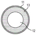
The conductive member according to the present invention includes a conductive substrate and a surface layer including a mesh-like structure provided thereon. Fig. 1A and 1B show an example of a conductive member according to the present invention. For example, as shown in fig. 1A, the conductive member according to the present invention may include a conductive mandrel 12 as a conductive base and a surface layer 11 including a mesh structure provided on the outer periphery of the conductive mandrel 12. For example, as shown in fig. 1B, the conductive member according to the present invention may include a conductive mandrel 12 as a conductive substrate, a conductive resin layer 13 provided on the outer periphery of the conductive mandrel 12, and a surface layer 11 including a mesh-like structure provided on the outer periphery of the conductive resin layer 13. As necessary, the conductive member may have a multilayer configuration including a plurality of conductive resin layers 13 within a range that does not inhibit the effect of an aspect of the present invention.
As shown in fig. 1A, the conductive member according to the present invention may include a conductive mandrel 12 as a conductive base and a surface layer 11 including a mesh structure provided on the outer periphery of the conductive mandrel 12. The configuration not including the conductive resin layer can prevent the generation of by-products by the interface reaction when energy is applied during discharge, thus contributing to the display of the effects of the present invention.
< conductive substrate >
As described above, the conductive substrate may include a conductive mandrel, or may include a conductive mandrel and a conductive resin layer provided on the outer periphery of the conductive mandrel. The conductive substrate according to the present invention may include a rigid structure from the viewpoint of stability of shape.
[ conductive core shaft ]
The conductive mandrel may be appropriately selected from known conductive mandrels used in the field of conductive members for electrophotography. A metal mandrel may be used. Examples include cylinders comprising carbon steel alloys with nickel plated surfaces having a thickness of about 5 μm. When the energy during discharge is partially converted into heat energy, the metal core shaft having high thermal conductivity facilitates the dissipation of the heat energy, reduces damage to the conductive member, and improves the durability thereof.
[ conductive resin layer ]
The conductive resin layer may be formed of a rubber material or a resin material. Any known rubber material in the field of conductive members for electrophotography can be used without limitation. Examples thereof specifically include the following rubber materials: epichlorohydrin homopolymers, epichlorohydrin-ethylene oxide copolymers, epichlorohydrin-ethylene oxide-allyl glycidyl ether terpolymers, acrylonitrile-butadiene copolymers, and hydrogenated products of acrylonitrile-butadiene copolymers; and silicone rubber, acrylic rubber, and urethane rubber. Any resin material known in the field of conductive members for electrophotography can be used. Specifically, examples thereof include polyurethane, polyamide, polyester, polyolefin, epoxy resin, and silicone resin. These materials may be used alone or in combination of two or more.
Among these materials for forming the conductive resin layer, acrylonitrile rubber can be used. This is because if the material is acrylonitrile rubber, the non-conductive fibers forming the mesh-like structure of the present invention have low reactivity, and are less likely to cause the generation of by-products and the accompanying discharge deterioration even if energy is applied during discharge.
The material for forming the conductive resin layer may be blended with an electron conductive agent or an ion conductive agent as necessary to control the resistance value. Examples of the electron conductive agent include carbon black and graphite having electron conductivity; oxides such as tin oxide; metals such as copper and silver; and conductive particles whose surfaces are coated with an oxide or a metal to have conductivity. Examples of the ion conductive agent include ion conductive agents having ion exchange properties such as quaternary ammonium salts and sulfonic acid salts having ion conductivity. These conductive agents may be used alone or in combination of two or more.
Fillers, softeners, processing aids, tackifiers, anti-blocking agents, dispersants, foaming agents, and roughening particles, which are generally used as compounding agents for resins, may also be added within a range not to impair the effects of one aspect of the present invention.
As a measure of the resistance value of the conductive resin layer, for example, the volume resistivity may be 1 × 10³Omega cm or more and 1X 10⁹Omega cm or less. It was confirmed that the surface layer including the mesh-like structure according to the present invention can reduce image defects due to excessive discharge even in the case where the resistance value of the conductive substrate is sufficiently low.
< surface layer comprising network Structure >
From the viewpoint of preventing abnormal discharge and maintaining discharge stability even in long-term use, the surface layer including the mesh structure may have the following configuration.
[ Properties of non-conductive fibers in surface layer including mesh Structure ]
The surface layer comprising the network structure comprises non-conductive fibers containing a radiation degradable resin. The surface layer comprising the mesh structure may comprise non-conductive fibres. The non-conductive fibers may comprise a radiation degradable resin. In the radiation-degradable resin, the molecular chain is more easily broken by irradiation with radiation than by a crosslinking reaction. The use of the non-conductive fiber containing a radiation degradable resin according to the present invention reduces discharge deterioration as described above. On the other hand, examples of resins having a strong tendency to have a molecular structure expanded by molecular crosslinking or the like rather than irradiation of a newly formed bond with radiation include radiation-crosslinking type resins. These radiation crosslinking resins generate stable free radicals to increase the chance of reaction with ambient oxygen, water, etc., thereby promoting oxidation and the formation of byproducts. Therefore, the resistance decreases during discharge, resulting in discharge degradation. In particular, at high temperature and high humidity, the resin molecules have increased mobility to promote reactions with its surrounding molecules. It should be noted that the resin material used as the fiber in the examples of Japanese patent application laid-open No.2015-68985 is a radiation crosslinking type resin which causes deterioration of discharge.
Examples of radiation-degradable resins can be found, for example, on pages 89 to 95 of "Hoshasen to kobunshi" by Kenichi Shinohara et al (published by Maki Shoten in 1968).
In the present invention, whether or not the resin corresponds to the radiation-degradable resin can be determined by measuring the molecular weight before and after the treatment of applying the radiation line or equivalent energy to examine the difference. For example, the target resin is subjected to corona discharge and analyzed by measurement by Gel Permeation Chromatography (GPC). In GPC measurement, a target resin is dissolved in a solvent to prepare a solution. In this step, the solvent which most easily dissolves the target resin may be appropriately selected from toluene, Tetrahydrofuran (THF), trifluoroacetic acid, 1,1,1,3,3, 3-hexafluoro-2-propanol (HFIP) and formic acid.
GPC measurement was performed on the solution, thereby measuring the resin component dissolved in the solution. The resin having a molecular weight equal to or less than that before the corona discharge treatment indicates that the breakage of the molecular skeleton occurs preferentially, and is judged as a radiation-degradable resin. On the other hand, the resin having an increased molecular weight is determined to be a radiation-crosslinking resin.
The glass transition temperature of the radiation-degradable resin is preferably 50 ℃ or higher and 200 ℃ or lower. The glass transition temperature is more preferably 80 ℃ to 200 ℃, and still more preferably 100 ℃ to 150 ℃. The glass transition temperature of 50 ℃ or more and 200 ℃ or less prevents the change of the network structure caused by the change of the fiber shape even when a large energy is applied in the form of thermal energy for a long time by discharge, thereby maintaining the discharge capability. Within this range, the higher the glass transition temperature, the more significantly the structural change is prevented. In particular, the glass transition temperature of 80 ℃ or higher minimizes the change of the network structure such as the change of the fiber shape even under the application of a high discharge energy or a high voltage to the conductive member side, thereby maintaining the discharge capability. Molecular motion can be active even at room temperature at glass transition temperatures of less than 50 ℃; in this case, the shape of the fiber may be changed by applying discharge energy to reduce the surface area, resulting in discharge degradation. On the other hand, at a glass transition temperature of more than 200 ℃, although the network structure has increased hardness around room temperature, the network structure may become brittle due to the microfibers forming the network structure, resulting in the network structure being damaged under the application of a slight stress. As a result, stable discharge cannot be maintained for a long time in some cases.
The glass transition temperature of the resin contained in the non-conductive fibers contained in the surface layer including the mesh-like structure can be measured as follows: the surface layer including the mesh-like structure is recovered from the conductive member with a pair of tweezers or the like, and measured by, for example, Differential Scanning Calorimetry (DSC). The DSC measurement may also be performed after the surface layer including the mesh-like structure is recovered from the conductive member, melted by heating or with a solvent, and formed into a sheet.
The radiation-degradable resin having a glass transition temperature within this range may be an acrylic resin having a structural unit represented by formula (1):
formula (1)

Wherein R is1Represents a hydrocarbon group having 1 to 6 carbon atoms. R1Preferably a hydrocarbon group having 2 to 6 carbon atoms, more preferably a linear or branched alkyl group having 2 to 6 carbon atoms. If R is1Is a straight-chain or branched alkyl group having 2 to 6 carbon atoms, then R1Does not have a cyclic structure, and therefore, stable radicals are prevented from being formed due to resonance or the like. R1Having more carbons increases steric hindrance, thereby reducing the chance of reaction with discharge products at that portion, preventing oxidation. Furthermore, R1At least one selected from the group consisting of the groups represented by the formulae (2) to (5):
formula (2)
-C(CH3)3
Formula (3)
-CH(CH3)2
Formula (4)
-CH(CH3)-C(CH3)3
Formula (5)
-C(CH3)2-CH(CH3)2。
If R is1Is at least one member selected from the group consisting of the groups represented by the formulae (2) to (5), then R1Has no secondary carbon atoms that readily become free radicals, and has a large steric hindrance to prevent oxidation. In particular, R1Can be-C (CH)3)3. If R is1is-C (CH)3)3Then R is1Having quaternary and primary carbon atoms and no tertiary carbon atoms. This structure is more remarkableThe formation of stable radicals is suppressed, and the discharge degradation due to oxidation is reduced. If R is1Containing more than 7 carbon atoms, then R1With a larger number of moieties that can be converted into radicals during discharge. In some cases, such groups may promote oxidation and the formation of byproducts by reacting with ambient oxygen and water.
Examples of the acrylic resin having the structural unit represented by formula (1) specifically include poly (methyl methacrylate), poly (ethyl methacrylate), poly (propyl methacrylate), poly (isopropyl methacrylate), poly (butyl methacrylate), poly (t-butyl methacrylate), poly (isobutyl methacrylate), and poly (benzyl methacrylate). Other examples of the acrylic resin having the structural unit represented by formula (1) include copolymers prepared from a combination of two or more monomers of the above-mentioned specific acrylic resin.
A possible reaction mechanism using the acrylic resin having the structural unit represented by formula (1) as the radiation-degradable resin will be described by the following formula (a). In formula (a), n represents the number of repeats, and the points represent radicals. The energy applied by the discharge dissociates hydrogen atoms in the methyl group bonded to the main chain polymer skeleton to generate radicals. Radicals are easily generated near the ends of the backbone. The radicals produced are very unstable under the influence of ester bonds having an electron-withdrawing action. Thus, in the next reaction, the radicals will migrate to other moieties. At this time, radicals migrate in the direction of the main chain skeleton due to the influence of ester bonds. The bond between the quaternary carbon atom bonded to the methyl group and the carbon adjacent thereto in the main chain skeleton direction is broken, and the adjacent carbon becomes a radical, resulting in molecular breakage. After the molecule cleavage, a main skeleton and a skeleton having a very short molecular chain are generated. The reaction is terminated on the main skeleton side, and radicals remain on the skeleton side having short molecular chains. The skeleton having the radical is further decomposed by further reaction. The free radicals disappear as a result of conversion to gas. Thus, the entire radical reaction is terminated. In other words, even if unstable radicals are generated, the reaction is rapidly terminated; therefore, it is considered that the chance of reacting with the surrounding oxygen and water is further reduced, preventing oxidation.
Formula (a)

The radiation-degradable resin may be a crystalline resin having a melting point of 50 ℃ or higher and 350 ℃ or lower. The melting point is preferably 100 ℃ or higher and 350 ℃ or lower, and more preferably 150 ℃ or higher and 350 ℃ or lower. Since the crystalline resin also has an amorphous portion, the resin preferably has a high glass transition temperature. However, if the resin having a low glass transition temperature has crystallinity and has a melting point of 50 ℃ or more and 350 ℃ or less, the shape of the crystalline portion is maintained even after thermal energy is applied by discharge, thereby reducing the change in the network structure and maintaining the discharge capability. In particular, in a resin having a melting point of 150 ℃ or higher, the influence of the amorphous portion is almost negligible. At a melting point of more than 350 ℃, although the network structure has increased hardness around room temperature, the network structure may become brittle due to the microfibers forming the network structure, resulting in damage of the network structure under application of a slight stress. As a result, in some cases, stable discharge cannot be maintained for a long time.
Melting points can be measured by Differential Scanning Calorimetry (DSC) or thermogravimetric differential thermal analysis (TG-DTA). Whether the resin has crystallinity can be judged from a melting point clearly observed or a crystal peak appearing in X-ray diffraction analysis (XRD).
Among these radiation-degradable resins having crystallinity, at least one selected from the group consisting of polysaccharides, polysaccharide derivatives and polyacetals can be used. The polysaccharide represents a polymer having a plurality of monosaccharide molecules bonded by glycosidic bonds. The polysaccharide derivative is a substance having a molecular structure including a glycoside bond and a monosaccharide molecular skeleton, and having a partially introduced functional group or substituted atom in a portion other than the glycoside bond and the monosaccharide molecular skeleton. In the polysaccharides, polysaccharide derivatives and polyacetals, the main chain skeleton of the molecular structure regularly contains C-O-C bonds of carbon atoms and oxygen atoms, and has repeating units formed by the C-O-C bonds. Therefore, when a radical is generated and then the reaction proceeds, any C-O bond is easily broken to terminate the reaction. As a result, the time of the whole reaction is shortened, and the progress of oxidation is prevented.
The polysaccharides and polysaccharide derivatives may be cellulose and cellulose derivatives, respectively. Cellulose and cellulose derivatives have a methyl group on a quaternary carbon atom and have a tertiary carbon atom adjacent to the quaternary carbon atom. Thus, the energy applied by the discharge generates radicals on the methyl groups, which migrate to the tertiary carbon atoms, or directly on the tertiary carbon atoms, to immediately cause the molecular cleavage of the glycosidic bond. In particular, since the structural units are alternately bonded to each other via glycosidic bonds, the above reaction proceeds selectively regardless of the application of energy. Therefore, the reaction time is further shortened, and discharge deterioration due to oxidation is reduced.
Among these radiation-degradable resins having crystallinity, cellulose acetate is particularly useful. The generation of radicals in hydroxyl groups is suppressed by partial or complete substitution of these groups with acetyl groups, thereby accelerating the migration of radicals, resulting in molecular cleavage of glycosidic bonds, and thus reducing discharge degradation due to oxidation.
Among these radiation-degradable resins having crystallinity, polyacetal may be used. The polyacetal does not have a bulky functional group, and energy applied by electric discharge is concentrated on a molecular main chain skeleton. As a result, the time required for the molecule cleavage is shortened, and oxidation is further suppressed.
The mesh structure may further include a radical scavenger (radicalcalgner) in addition to the non-conductive fibers. The addition of the radical scavenger results in a rapid termination of the radical reaction during the generation of radicals by the application of discharge energy. Therefore, the chance of molecular cleavage is reduced, thereby suppressing the decrease in molecular weight. The radical scavenger may be an antioxidant having the effect of preventing the formation of peroxides by air oxidation, such as p-hydroquinone or 3, 5-dibutyl-4-hydroxytoluene. The amount of the radical scavenger added may be 10% by mass or less based on the amount of the radiation-degradable resin. The amount of the radical scavenger added in this range can reduce the influence of the radical scavenger on the mechanical strength of the network structure, and only the effect of reducing the discharge deterioration can be achieved.
The weight average molecular weight (Mw) of the radiation-degradable resin is preferably 50000 or more and 2500000 or less, more preferably 150000 or more and 2500000 or less, and further more preferably 300000 or more and 2500000 or less. The resin having a weight average molecular weight of 50000 or more and 2500000 or less has hardness derived from a high molecular weight. Therefore, the mesh structure is less likely to change even if used for a long time, and stable discharge can be maintained. In particular, a resin having a weight average molecular weight of 150000 or more prevents the damage of the network structure even in the case where a charging member including this resin is used for a long time (while being in contact with other members).
The weight average molecular weight can be determined as follows: the surface layer including the mesh-like structure is recovered from the conductive member with a pair of tweezers, and measured by, for example, micro-sampling mass spectrometry (μ -MS) or Gel Permeation Chromatography (GPC). The micro-sampling mass spectrometry may be performed after the surface layer including the mesh-like structure is recovered from the conductive member, melted by heating or with a solvent, and formed into a sheet.
The network structure may further contain a resin having a low molecular weight Mw of less than 50000, in addition to the high molecular weight resin as the radiation-degradable resin. As described above, energy applied by electric discharge easily generates radicals in the vicinity of the terminal of the molecular skeleton, and the molecule is cleaved in the vicinity of the terminal. The low-molecular-weight resin added has a larger number of terminals in the molecular skeleton than the high-molecular-weight resin (matrix resin) mainly forming a network structure. Therefore, the energy applied by the electric discharge causes selective molecular cleavage on the molecular skeleton of the added low-molecular-weight resin. Therefore, it is possible to prevent the molecules of the resin mainly forming the network structure from being broken, maintain the molecular structure, and further reduce discharge deterioration. From the viewpoint of enhancing the effect of reducing discharge deterioration, the weight average molecular weight of the low-molecular weight resin may be 10000 or less. The low molecular weight resin may have the same repeating unit as the matrix resin. This is because the compatibility between the low-molecular-weight resin and the matrix resin is enhanced to uniformly disperse the low-molecular-weight resin in the network structure. The content of the low-molecular-weight resin is 10 mass% or less with respect to the matrix resin. The content of the low-molecular-weight resin in this range reduces the influence of the low-molecular-weight resin on the mechanical strength of the network structure, and only the effect of reducing discharge deterioration is achieved.
The non-conductive fiber has a volume resistivity of 1X 10⁸A fiber having an omega cm or more. The volume resistivity is preferably 1X 10⁸To 1X 10¹⁶Omega. cm, more preferably 1X 10¹¹To 1X 10¹⁶Omega. cm, more preferably 1X 10¹³To 1X 10¹⁶Ω·cm。
At less than 1X 10⁸At a volume resistivity of Ω · cm, the charge leaks to the conductive substrate to suppress the charge, resulting in discharge degradation. Volume resistivity in this range can in some cases lead to local concentration of the discharge energy in the fiber; if the discharge energy is converted into heat energy, the fibers are thermally broken to cause discharge deterioration. On the other hand, 1X 10⁸The volume resistivity of Ω · cm or more reduces discharge degradation without leaking the charge into the conductive matrix. The volume resistivity in this range also suppresses the generation of unexpected abnormal discharge resulting from discharge from the surface layer itself including the network structure, prevents local concentration of discharge energy within the fiber, and thus prevents discharge degradation.
1×10¹⁶The volume resistivity reduction of Ω · cm or less is attributed to discharge failure including increased resistance of the surface layer of the network structure. At 1X 10⁸The nonconductive fiber according to the present invention may contain 0.1 to 5 parts by mass of an ion conductive agent per 100 parts by mass of the radiation degradable resin at a volume resistivity of Ω · cm or more. 1X 10¹¹The volume resistivity of Ω · cm or more can sufficiently prevent unexpected abnormal discharge from the surface layer including the mesh structure. In addition, in 1 × 10¹³Almost no unexpected abnormal discharge from the surface layer including the network structure was observed at a volume resistivity of Ω · cm or more.
The volume resistivity of the non-conductive fibers can be measured by the following method. The surface layer including the mesh-like structure was recovered from the conductive member with a pair of tweezers. A cantilever of a Scanning Probe Microscope (SPM) is brought into contact with a single fiber to sandwich the single fiber between the cantilever and a conductive substrate. So that the volume resistivity can be measured. Alternatively, the surface layer including the mesh-like structure is recovered from the conductive member, melted by heating or with a solvent, and formed into a sheet. The sheet can also be used to measure volume resistivity.
The volume resistivity of the conductive member is prevented from being lowered even after the discharge treatment is performed for a long time under high-temperature and high-humidity conditions. Therefore, the charging ability of the surface layer including the mesh structure is maintained, thereby maintaining the discharge ability and reducing the discharge deterioration.
[ shape of non-conductive fiber in the layer of network Structure ]
The non-conductive fibers forming the surface layer including the mesh-shaped structure according to the present invention may have a length greater than 100 times the diameter of the fibers. From the observation of the surface layer including the network structure with an optical microscope or the like, it was confirmed whether the fiber length was more than 100 times the fiber diameter. The fibers may have any cross-sectional shape, such as circular, elliptical, rectangular, polygonal, or semi-circular. The fibers may have different shapes in any cross-section. If the fiber has a cylindrical shape, the fiber diameter represents the diameter of a circle of the fiber cross-section, and if the fiber has a non-cylindrical shape, the fiber diameter represents the length of the longest straight line passing through the center of gravity in the cross-section of the fiber.
The average fiber diameter d of the nonconductive fibers may be 0.2 μm or more and 15 μm or less. The average fiber diameter d of 15 μm or less ensures a large surface area with respect to the amount of the resin forming the fibers, thereby increasing the charge amount, thereby increasing the discharge capacity. Further, if the discharge energy is converted into heat, the sufficiently ensured surface area contributes to heat diffusion to the outside of the fiber, preventing fiber deformation or deterioration of the material forming the fiber due to abnormal accumulation of heat. The average fiber diameter d is more preferably 2.5 μm or less, and still more preferably 1.5 μm or less. The average fiber diameter d of 2.5 μm or less reduces abnormal accumulation of heat. At an average fiber diameter d of 1.5 μm or less, the abnormal accumulation of heat is almost negligible. On the other hand, even if the polymer forming the surface portion of the fiber has a significantly reduced molecular weight, an average fiber diameter d of 0.2 μm or more can maintain the molecular weight of the resin forming the center of the fiber, thereby preventing deformation of the fiber, thereby preventing discharge deterioration. The average fiber diameter d is more preferably 0.3 μm or more, and still more preferably 0.4 μm or more.
The average fiber diameter d can be confirmed from direct observation of the fiber by measurement by an optical microscope, a laser microscope, or a Scanning Electron Microscope (SEM). In the present invention, the surface of the surface layer including the mesh-like structure according to the present invention was observed using SEM, and the fiber diameter of any 100 fibers was measured. In the present invention, the average of the fiber diameters of any 100 fibers is the average fiber diameter d.
[ distance between fibers of network Structure ]
When the surface of the conductive member is observed, at least a part of the mesh-like structure may be present in any square region of 200 μm square.
If the surface layer including the mesh-like structure has an appropriate distance between fibers, the amount of charge during the application of voltage to the conductive member is increased to secure the discharge capability. Further, since the discharge is mainly performed by the mesh-shaped structure, and the discharge position is dispersed to reduce the size of the discharge, a stable discharge is realized. On the other hand, an excessively large inter-fiber distance increases the chance of discharge from the conductive matrix. In this case, the interface between the conductive substrate and the mesh-like structure receives an excessively large amount of discharge energy, and adhesion at the interface is reduced in some cases. The influence of such a decrease in adhesion caused at one position further increases the chance of discharge from the conductive substrate, resulting in a decrease in adhesion at many positions. As a result, the mesh structure may be changed to reduce the surface area, resulting in discharge degradation in some cases. Therefore, the distance between fibers in the surface layer including the mesh structure may be 200 μm or less. In order to realize a distance between fibers of 200 μm or less, at least a part of the mesh-like structure is present in an arbitrary square region of 200 μm square when the surface of the conductive member is observed. Specifically, when the surface of the surface layer including the mesh-like structure was observed in the vertical direction with an optical microscope, a laser microscope or the like, arbitrary 100 square regions of 200 μm square (length: 200 μm, width: 200 μm) were measured. The requirement is satisfied if at least a part of the mesh-like structure can be confirmed at all 100 measurement positions. The image to be observed has integrated information of all pieces of information in the thickness direction including the surface layer of the mesh-like structure. It is considered that the above-described measurement method can be used without problems because the inter-fiber distance on the surface of the surface layer including the mesh-like structure containing information in the thickness direction affects the effect of reduction of discharge deterioration.
When the surface of the conductive member is observed, it is more preferable that at least a part of the mesh-like structure is present in an arbitrary square region of 100 μm square. In a structure in which at least a part of the mesh structure is observed in any square area of 100 μm square, the adhesion between the mesh structure and the conductive substrate is prevented from being lowered. In addition, the mutual complementation of the fibers forming the network structure suppresses the change of the network structure, further reducing the discharge degradation.
[ thickness of surface layer including network Structure ]
As for the thickness of the surface layer including the mesh-like structure, the average layer thickness t of the surface layer including the mesh-like structure may be 1 μm or more and 50 μm or less. Even if the polymer forming the surface of the fiber has a reduced molecular weight due to discharge, an average layer thickness t of 1 μm or more can maintain the molecular weight of the polymer forming the inside of the fiber; as a result, the fibers retain their shape. Thereby maintaining the mesh structure and reducing discharge degradation. In contrast, at a large average layer thickness t, a part of the mesh structure may exhibit the same action as a film without any voids, thereby locally causing a large discharge around it; in this case, energy is locally concentrated to cause a rapid decrease in molecular weight. Such a rapid decrease in molecular weight due to discharge failure caused by the conductive member serving as an insulator may cause deformation of the network structure, resulting in discharge degradation. However, an average layer thickness t of 50 μm or less can prevent these problems from occurring. The average layer thickness t is more preferably 1 μm or more and 30 μm or less, and still more preferably 2 μm or more and 20 μm or less. In particular, the average layer thickness t of 30 μm or less further enhances the effect of holding voids in the network structure, preventing a local decrease in molecular weight.
The thickness of the surface layer including the mesh-like structure means the thickness of the surface layer including the mesh-like structure measured perpendicular to the surface of the conductive substrate. The thickness represents the thickness of the region containing the non-conductive fibers in the member used, regardless of whether the member is in contact with or out of contact with other members. The thickness can be measured as follows: a slice including the conductive base and the surface layer including the mesh-like structure was cut out of the conductive member and measured by X-ray CT measurement. The average layer thickness t represents an average value of thicknesses at a total of 25 positions where the conductive member is divided into 5 equal parts in the length direction and the thicknesses are measured at arbitrary 5 positions in each of the 5 equal parts.
[ method for Forming surface layer including network Structure ]
Examples of the forming method of the surface layer including the mesh-like structure include, but should not be limited to, the following methods: fibers are produced from a raw material solution for fibers by an electrospinning method (electric field spinning/electrostatic spinning), a composite spinning method, a polymer blend spinning method, a melt-blown spinning method, a flash spinning method, or the like, and the produced fibers are laminated on the surface of a conductive substrate. The fibers thus produced all have a sufficient length relative to the fiber diameter. The electrospinning method is a method of producing fibers in which a high voltage is applied between a raw material solution contained in a syringe and a collector electrode (collector) to electrically charge the solution extruded from the syringe, and the solution flies into fine lines in an electric field, which are attached to the collector as fibers.
Among these methods of forming the surface layer including the network structure, an electrospinning method may be used. In other words, the method for producing the electroconductive member for electrophotography according to the present invention may include forming the surface layer including the mesh-like structure by an electrospinning method. One example of a method of forming a surface layer including a mesh-like structure by an electrospinning method will be described with reference to fig. 2. As shown in FIG. 2, the electrospinning apparatus includes a high voltage power supply 25, a raw material solution storage tank 21, and a spinneret 26. The equipment mounted collector 23 is typically grounded to ground 24. The raw material solution is extruded from the tank 21 to the spinneret 26 at a predetermined speed. A voltage of 1 to 50kV is applied to the spinneret 26. When the electric attraction force exceeds the surface tension of the raw material solution, the jet 22 of the raw material solution is ejected toward the collector 23. The raw material solution may be a raw material solution containing a solvent and a resin that is melted by heating the resin material to a temperature of the melting point or higher. If the feed solution is a solvent-containing feed solution, the solvent in jet 22 gradually volatilizes. In this process, the charge per unit volume in the raw material solution increases; thus, the solution will break up more finely and in some cases travel into a collector. When the jet reaches the collector 23, the size of the jet is reduced to the nanometer scale.
As shown in fig. 2, if the conductive substrate is used as the collector 23, the conductive member including the surface layer including the mesh-like structure formed on the outer peripheral surface of the conductive substrate can be directly manufactured. The conductive substrate grounded to the ground reduces local unevenness of the potential on the surface thereof, thereby forming a uniform mesh structure. This method of directly forming the surface layer including the mesh-like structure on the surface of the conductive substrate can form a uniform mesh-like structure with reduced unevenness in density and thickness, as compared with a method of winding the deposited fiber material around the surface of the conductive substrate. In the production of fibers by the electrospinning method, the fibers moving toward the collector are charged. Thus, the plurality of fibers are deposited at an angle to each other due to electrostatic forces resulting from the electrical charge of the fibers. Such deposition of fibers is advantageous in terms of maintenance of fiber diameter and formation of voids.
The raw material solution for the electrospinning method can be suitably prepared by any known method. The raw material solution may contain any kind of solvent at any content as long as the raw material solution is most suitable for the electrospinning method. In order to uniformly form the surface layer including the mesh structure on the outer peripheral surface of the conductive substrate, the spinneret and the conductive substrate may be moved relative to each other in any direction, or the conductive substrate may be rotated. In this case, the orientation of the fibers is reduced by setting the fiber forming speed higher than the relative moving speed between the spinneret and the surface of the conductive substrate facing the spinneret. Such fibers having a reduced orientation may enhance the flexibility of the surface layer including the mesh structure and have high adhesion during expansion and contraction of the fibers due to temperature and/or humidity. The fiber formation rate indicates the length of the fiber formed on the conductive matrix per unit time.
(processing box)
A process cartridge according to an aspect of the present invention is configured to be detachably mounted to a body of an electrophotographic image forming apparatus, and includes a conductive member according to an aspect of the present invention.
Fig. 3 shows an example of the process cartridge. The process cartridge shown in fig. 3 includes a developing device and a charging device. The developing device includes a developing roller 33 and a toner container 36 that accommodates toner 39. The developing device may include the toner supply roller 34, the developing blade 38, and the stirring blade 310, as necessary.
The charging device includes a photosensitive drum 31, a cleaning blade 35, and a charging roller 32. The charging device may further include a waste toner container 37.
Voltages are applied to the charging roller 32, the developing roller 33, the toner supply roller 34, and the developing blade 38, respectively. The conductive member according to an aspect of the present invention may be used for any of the charging roller 32, the developing roller 33, and the toner supply roller 34. In particular, it is suitable to use the conductive member as the charging roller 32.
(electrophotographic image forming apparatus)
An electrophotographic image forming apparatus according to an aspect of the present invention includes an electroconductive member according to an aspect of the present invention. Fig. 4 shows one example of an electrophotographic image forming apparatus. The electrophotographic image forming apparatus shown in fig. 4 includes the process cartridges shown in fig. 3 for Black (BK), magenta (M), yellow (Y), and cyan (C) toners, respectively. These cartridges are detachably mounted to the color image forming apparatus.
The photosensitive drum 41 rotates in the arrow direction to be uniformly charged by a charging roller 42 having a voltage applied from a charging bias power source. An electrostatic latent image is formed on the surface of the photosensitive drum with the exposure light 411. On the other hand, the toner 49 contained in the toner container 46 is supplied to the toner supply roller 44 by the stirring blade 410, and is conveyed to the developing roller 43. The toner 49 is uniformly applied on the surface of the developing roller 43 by the developing blade 48 disposed in contact with the developing roller 43. The toner 49 is also charged by frictional charging. The electrostatic latent image is developed by toner 49 conveyed by developing roller 43 disposed in contact with photosensitive drum 41, and visualized as a toner image. The visualized toner image on the photosensitive drum 41 is transferred onto the intermediate transfer belt 415 by the primary transfer roller 412 having a voltage applied by the primary transfer bias power supply. The intermediate transfer belt 415 is driven by a tension roller 413 and an intermediate transfer belt driving roller 414. The toner images of the four colors are sequentially superimposed, thereby forming a color image on the intermediate transfer belt 415.
The transfer material 419 is fed into the apparatus by a paper feed roller, and is conveyed between the intermediate transfer belt 415 and the secondary transfer roller 416. The secondary transfer roller 416 receives a voltage from a secondary transfer bias power source, and transfers the color image on the intermediate transfer belt 415 onto a transfer material 419. The transfer material 419 to which the color image is transferred is fixed by a fixing unit 418, and is discharged to the outside of the apparatus. The printing operation is then terminated.
On the other hand, the untransferred toner remaining on the photosensitive drum 41 is scraped off from the surface of the photosensitive drum 41 by the cleaning blade 45, and is stored in the waste toner container 47. The cleaned photosensitive drum 41 is repeatedly used to perform the above steps. The untransferred toner remaining on the intermediate transfer belt 415 is also scraped off by a cleaning device 417.
According to an aspect of the present invention, a conductive member for electrophotography that can maintain high discharge performance even when used under a high-temperature and high-humidity environment can be obtained. According to another aspect of the present invention, it is also possible to obtain a process cartridge and an electrophotographic image forming apparatus which can stably form a high-quality electrophotographic image.
Practice ofExample (b)
< example 1>
[1. preparation of conductive substrate ]
A conductive mandrel (core metal) was prepared as a conductive substrate. A bar made of free-cutting steel was prepared. The rod has a total length of 252mm and a gradually changing outer diameter. In the rod, the outer diameter of the central region of 230mm (excluding the region 11mm from both ends) was 8.5mm, and the outer diameter of the region 11mm from both ends was 6 mm. In the embodiment, a conductive mandrel (core metal) is used as the conductive roller.
[2. preparation of coating liquid for surface layer including network Structure ]
< preparation of coating liquid 1>
Poly (t-butyl methacrylate) (PtBMA) (manufactured by Sigma-Aldrich Corporation, weight average molecular weight: 170000) was prepared as a material for the non-conductive fibers.
PtBMA was dissolved in a solvent N, N-Dimethylacetamide (DMAC) (manufactured by KISHIDA CHEMICAL co., ltd., extra grade) and the solid content was adjusted to 20 mass%, thereby preparing a coating liquid 1 for forming a surface layer.
< preparation of coating solutions 2 to 25 >
Coating liquids 2 to 25 were prepared in the same manner as coating liquid 1 except that the materials for the non-conductive fibers, the solvents, and the solid contents were changed as shown in tables 1-1 and 1-2.
TABLE 1-1

Tables 1 to 2

PtBMA: poly (tert-butyl methacrylate) (R)1:-C(CH3)3);
PMMA: poly (methyl methacrylate) (R)1:-CH3);
PEMA: poly (ethyl methacrylate) (R)1:-CH2CH3);
PBMA: poly (butyl methacrylate) (R)1:-CH2CH2CH2CH3);
PiBMA: poly (isobutyl methacrylate) (R)1:-CH2CH(CH3)2);
PiPMA: poly (isopropyl methacrylate) (R)1:-CH(CH3)2);
P (B-iB) MA: butyl methacrylate-isobutyl methacrylate copolymers;
p (B-E) MA: butyl methacrylate-ethyl methacrylate copolymers;
PCMA: poly (cyclohexyl methacrylate) (R)1:-C6H11);
PIB: polyisobutylene;
PMS: poly (alpha-methylstyrene);
POM: a polyacetal;
PS: polystyrene;
PBenMA: poly (benzyl methacrylate);
DMAC: n, N-dimethylacetamide;
HFIP: 1,1,1,3,3, 3-hexafluoro-2-propanol.
[3. preparation of electroconductive Member ]
Next, coating liquid 1 was jetted by an electrospinning method, and the resulting microfibers were directly wound around a conductive roll which was a conductive substrate mounted as a collector. Thereby, the conductive member 1 including the surface layer including the mesh structure on the outer peripheral surface of the conductive substrate was prepared.
In other words, first, a conductive roller as a collector was mounted to an electrospinning apparatus (manufactured by MECC co., ltd., trade name: NANON-01). Next, coating liquid 1 was filled into the tank. The can was set to a distance of 17cm from its end to the conductive roller. The temperature was 33 ℃ and the relative humidity was 20%. The electrospinning apparatus was horizontally moved at 10mm/s while applying a voltage of 22kV to the spinneret, and the coating liquid 1 was ejected toward the conductive roller. At this time, the conductive roller as a collector was rotated at 50 rpm. Coating liquid 1 was jetted for 200 seconds, thereby preparing conductive member 1 including a surface layer including a network structure. Further, a plurality of conductive members 1 were also prepared for evaluation. In table 5, the rotation number (rpm) of the catcher is referred to as "ES rotation number (rpm)" and the spraying time of the coating liquid is referred to as "ES treatment time (sec)". These conditions are summarized in table 5.
[4. evaluation of characteristics ]
Next, the obtained conductive member was evaluated in the following evaluation test. The evaluation results are summarized in table 5.
(evaluation 4-1. confirmation of radiation degradability of non-conductive fiber)
This evaluation determines whether or not the resin particles forming the surface layer according to the present invention are formed of a radiation-degradable resin. In order to verify that the resin particles are formed of the radiation-degradable resin, first, the resin particles forming the surface layer were sampled from the conductive member for electrophotography immediately after the preparation without performing corona discharge. The molecular weight of the resin forming the resin particles was measured by Gel Permeation Chromatography (GPC). In the next step, the conductive member for electrophotography is subjected to corona discharge treatment by a predetermined method. The resin particles forming the surface layer of the conductive member for electrophotography were then sampled, and the molecular weight was measured by GPC. From the difference in molecular weight before and after the corona discharge, it was judged whether or not the resin contained in the resin particles was a radiation-degradable resin. Details will now be described.
First, a 5mg sample was taken from the surface layer of the conductive member a1 immediately after preparation (not subjected to corona discharge). The solvent which easily dissolves the sample is selected from the group consisting of toluene, chlorobenzene, Tetrahydrofuran (THF), trifluoroacetic acid and 1,1,1,3,3, 3-hexafluoro-2-propanol (HFIP), thereby preparing a1 mass% sample solution. A sample extracted from the mesh-like structure of the conductive member 1 according to example 1 was dissolved in toluene as a solvent.
The molecular weight was measured using the sample solution prepared above under the following conditions. The column was stabilized in a heated chamber at a temperature of 40 ℃ and the solvent used to dissolve the sample was passed through the column as eluent at this temperature at a flow rate of 1 mL/min. The sample solution (100. mu.L) was injected into the column. As for the molecular weight of the sample, the molecular weight distribution of the sample was calculated from the relationship between the logarithmic value of the calibration curve prepared from several monodisperse polystyrene standard samples (trade names: TSK gel standard polystyrene "0005202" to "0005211", manufactured by Tosoh Corporation) and the retention time. The GPC apparatus used was a GPC gel permeation chromatograph (trade name: HLC-8120, manufactured by Tosoh Corporation). The detector used was a differential refractive index detector (trade name: RI-8020, manufactured by Tosoh Corporation). The column used was a combination of three commercially available polystyrene GEL columns (trade name: TSK-GEL SUPER HM-M, manufactured by Tosoh Corporation). The molecular weight Mw of the sample extracted from the network structure of the conductive member 1 before the corona discharge treatment was 170000.
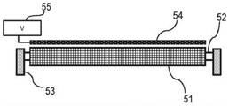
Subsequently, the conductive member a1 was subjected to corona discharge treatment using a corona discharge surface treatment apparatus (manufactured by KASUGA ELECTRIC WORKS ltd.). The corona discharge treatment was carried out in an H/H environment (an environment with a temperature of 30 ℃ and a relative humidity of 80%).
The method of performing corona discharge will be described in detail with reference to fig. 5. The conductive member 51 is fixed at both ends 52 thereof by support portions 53. The length direction of the aluminum corona electrode 54 is set to be parallel to the length direction of the conductive member 51, and the surface of the corona electrode 54 faces the surface of the conductive member 51. In the conductive member 1, the distance between the surface of the corona electrode 54 and the surface of the conductive member 51 at the closest region thereof was 1 mm. The support 53 was rotated at 30rpm/min to rotate the conductive member 51, and a state in which a voltage of 8KV was applied from the power supply 55 to the electrode was continued for 2 hours. Subsequently, a 5mg sample was extracted from the mesh structure of the conductive member 51 to measure a weight average molecular weight (Mw) by GPC using the same method. The sample is judged to be a radiation degradable resin if the weight average molecular weight Mw of the sample extracted from the conductive member after corona discharge is equal to or lower than the weight average molecular weight Mw of the sample extracted from the conductive member before corona discharge. In contrast, if the weight average molecular weight Mw before corona discharge is larger than the weight average molecular weight Mw after corona discharge, the sample is determined to be a radiation crosslinking type. The network structure of the conductive member 1 contains 0 mass% of an insoluble component. The weight average molecular weight Mw was 165000. Therefore, the non-conductive fibers forming the mesh structure of the conductive member 1 are made of a radiation degradable resin. In the evaluation results of tables 5 to 9 described later, the case where the sample was judged as a radiation-degradable resin was represented as "Y", and the case where the sample was not a radiation-degradable resin was represented as "N".
(evaluation 4-2 measurement of fiber diameter of non-conductive fiber)
The fiber diameter of the non-conductive fibers forming the surface layer including the mesh-like structure was measured using a Scanning Electron Microscope (SEM) (manufactured by Hitachi High-Technologies Corporation, trade name: S-4800, observed at 2000 times). First, a minute amount of the surface layer including the network structure is peeled from the conductive member 1, and platinum is deposited on the surface of the peeling sheet including the surface layer of the network structure. Next, the surface layer including the mesh structure on which platinum was deposited was embedded in an epoxy resin. A section thereof was cut with a microtome for SEM observation. In the SEM observation, 100 fibers having a cross-sectional shape close to a circle were randomly selected to measure the diameters of the fibers. The average of the measured fiber diameters of 100 fibers was defined as an average fiber diameter d.
(evaluation 4-3 measurement of volume resistivity of non-conductive fiber)
The volume resistivity of the non-conductive fibers forming the surface layer including the mesh-shaped structure was measured in a contact mode using a Scanning Probe Microscope (SPM) (manufactured by Quantum Instrument Corporation, trade name: Q-Scope 250). First, the surface layer including the mesh-like structure was recovered from the conductive member 1 using a pair of tweezers, and placed on a metal plate made of stainless steel. The measurement was performed in an environment at a temperature of 25 ℃ and a humidity of 50%. Next, individual fibers were selected that directly contacted the stainless steel plate. The cantilever of the SPM is brought into contact with the single fiber. A voltage of 50V was applied to the cantilever to measure the current value. The resistance value is calculated from the current value. Next, a volume value was calculated from the average fiber diameter d obtained by the method described in (4-2) and the contact area with the cantilever, and the resistance was converted into volume resistivity. The above measurements were taken at any 5 points and the average was defined as the volume resistivity of the non-conductive fibers.
(evaluation 4-4. distance between fibers of network Structure)
The distance between fibers in the surface layer including the mesh-like structure was measured by the following method. In the conductive member 1, the outer surface of the surface layer including the mesh structure was observed from the vertical direction using a laser microscope (manufactured by Keyence Corporation, trade name: VX 100). When observed with a laser microscope, 100 square regions of 100 μm square or 200 μm square were randomly selected, and it was confirmed whether or not a part of the fiber was observed in each of the 100 square regions. The distance between fibers in the surface layer comprising the network structure was evaluated according to the following criteria:
grade A: a part of the fibers was observed in all 100 square areas of 100 μm square.
Grade B: a portion of the fibers was observed in all 100 square areas of 200 μm square.
(evaluation 4-5 average layer thickness t of surface layer including network Structure)
The average layer thickness t of the surface layer including the network structure was evaluated by the following method. A part of the surface layer of the conductive member 1 including the mesh structure is removed using a microtome to expose the conductive base from the surface. A 200-fold objective lens was mounted on a laser microscope (manufactured by Keyence Corporation, trade name: VK-X100) to observe the conductive member 1, and respective focus positions of the surface of the conductive substrate and the surface of the surface layer including the surface of the mesh structure were determined. From the difference in focal position, the thickness of the surface layer including the mesh-like structure was calculated. The operation is performed at arbitrary ten positions of the conductive member 1, and the average value of the thicknesses of the ten positions obtained is defined as an average layer thickness t including the surface layer of the mesh-like structure.
(evaluation 4-6 measurement of glass transition temperature)
The glass transition temperature of the resin contained in the non-conductive fibers forming the surface layer including the network structure was evaluated by the following method. First, since a large amount of non-conductive fibers is required to directly evaluate the glass transition temperature from the surface layer of the conductive member 1 including the network structure, the coating liquid 1 was heated to 80 ℃ to volatilize the solvent, thereby preparing a 3mg sample for easy evaluation. The sample was measured by differential scanning calorimetry (manufactured by Yamato Scientific co., ltd., trade name: DSC7020 AS). The sample was left at-130 ℃ for 30 minutes; then, the input and output of thermal energy were measured while changing the temperature to 250 ℃ at a temperature-increasing rate of 10 ℃/min. The glass transition temperature was determined from the data obtained in the measurement using analysis software attached to a differential scanning calorimeter. In order to check the appropriateness of the glass transition temperature determined herein, 1mg of the surface layer including the mesh-like structure was peeled from the plurality of conductive members 1 and measured by the same method. As a result, the same glass transition temperature was obtained. From these results, the glass transition temperature measured by differential scanning calorimetry of a sample prepared by volatilizing the solvent of the coating liquid 1 as a raw material of the non-conductive fiber forming the surface layer including the network structure is defined as the glass transition temperature of the resin contained in the non-conductive fiber of the conductive member 1. In the examples described later, the same operations were performed to determine the glass transition temperature.
(evaluation 4-7. determination of crystalline resin and measurement of melting Point)
The crystallinity of the non-conductive fibers forming the surface layer including the network structure was determined by measuring the melting point using a thermogravimetric and differential thermal analyzer (TG-DTA) (manufactured by Rigaku Corporation, trade name: TG 8120). In other words, the resin showing the melting point in the measurement is judged as a crystalline resin. Specifically, the surface layer including the mesh-like structure is peeled off from the conductive member 1, and put into a dedicated sample holder made of aluminum. The sample holder is placed into an analyzer. The temperature was raised from room temperature to 500 ℃ at a rate of 10 ℃/min. The melting point was confirmed from the change in mass of the resin. If the resin decomposes without showing a clear melting point, the resin is judged not to be crystalline. The values of the melting points shown in table 5 of the evaluation results in this case are represented by the oblique lines (/).
[ evaluation 5 evaluation of durability against discharge deterioration ]
The durability of the charging ability of the conductive member 1 was evaluated by the following method. A laser printer (trade name: Laserjet Enterprise Color M553dn, manufactured by Hewlett-Packard Company) was prepared as an electrophotographic image forming apparatus. At this time, the output speed of the recording medium was changed to 300mm/sec, and the image resolution was changed to 1200 dpi.
First, the charging roller is detached from the process cartridge for the laser printer, and the conductive member 1 is attached thereto as the charging roller. The facing distance (facing distance) between the conductive member 1 and the photosensitive drum was adjusted to 100 μm at the closest position.
An apparatus capable of measuring the surface potential of a photosensitive drum is assembled into a process cartridge. The apparatus was equipped with a probe (manufactured by Trek Japan k.k. trade name: Model555P-1) connected to an electrostatic voltmeter (manufactured by Trek Japan k.k. trade name: Model 347). The measuring portion of the probe was disposed facing the surface of the photosensitive drum at a distance of 1.0 mm.
The cartridge was left to stand in an H/H environment (an environment having a temperature of 30 ℃ and a relative humidity of 80%) for 48 hours. In the next step, the process cartridge is mounted to the laser printer.
Evaluation was performed by the following method. An external power supply (trade name: Model 615; manufactured by Trek Japan KK) was used under an H/H environment (environment with a temperature of 30 ℃ and a relative humidity of 80%) to apply a direct-current voltage of 1200V to the core metal of the conductive member 1 and output a solid white image. The images were output to 2000 sheets a day, and 24 hours after the first sheet was output, the images were output to 2000 sheets again. This operation was performed for 5 days, thereby outputting the image to 10000 sheets in total. During this operation, the surface potential of the photosensitive drum is continuously measured. The difference (Δ Vd) between the surface potential of the photosensitive drum when the image is output on the first sheet and the surface potential of the photosensitive drum when the image is output on the 10000 th sheet is obtained1200) As the amount of the deterioration potential.
In table 9 (described later) showing the evaluation results, a case in which the surface of the photosensitive drum cannot be charged during the image output onto the first sheet due to insufficient discharge from the conductive member was evaluated as "NW" (not operating).
If Δ Vd at an applied voltage of 1200V at the time of evaluation1200When the voltage is 10V or less, the same evaluation as described above is performed to obtain the deteriorated potential amount (Δ Vd) except that the applied voltage is 1500V1500). In table 9 (described later) showing the evaluation results, "-" (hyphen) indicates that Δ Vd was not measured in the comparative example1500The value of (c).
[ evaluation 6 evaluation of volume resistivity change in durability evaluation ]
In order to confirm the change in the material of the network structure, the change in the volume resistivity before and after the durability evaluation at 1200V in [5] was measured. After the durability evaluation at 1200V, similarly to [4-3], the volume resistivity was measured at an environment of 25 ℃ and 50% humidity. From the results, the reduction ratio (%) was calculated from the evaluation in [4-3 ]. The two-digit or more decrease in volume resistivity indicates a decrease rate of 99% or more. This case is represented as "99-" in table 9 (described later) showing the evaluation results.
[ evaluation 7 evaluation of surface area change in durability evaluation ]
In [5] the conductive member for evaluation of durability at 1500V, durability of the shape of the mesh structure was confirmed by the following method. In other words, changes in surface area before and after durability evaluation at 1500V were examined by image analysis. The conductive member subjected to the evaluation [5] only at 1200V and not at 1500V was not subjected to the evaluation, and is represented by- (hyphen).
Image analysis was performed using a laser microscope (manufactured by Keyence Corporation, trade name: VK-X100). In the evaluation [5]Previously, 280 μm × 210 μm area images on the surface of the conductive member 1 were acquired at 100 areas by a laser microscope equipped with a 50-fold objective lens. Subsequently, in the evaluation [5]]After that, the surface of the conductive member 1 was photographed at 100 areas in the same manner. The surface area was calculated using image analysis software attached to the laser microscope to find the surface area to 28 taking into account the information of the image in the depth directionArea ratio (surface area/area) of 0 μm × 210 μm. This value is called S/S0. Calculation of S/S before and after durability evaluation0The ratio (%) of decrease in (c).
< examples 2 to 22>
A plurality of conductive members 2 to 22 were prepared in the same manner as in example 1 except that the coating liquid and the formation conditions were changed as shown in tables 5 to 7 at the time of forming the surface layer including the network structure, and evaluated in the same manner as in example 1. The evaluation results are shown in tables 5 to 7.
< example 23>
A conductive member 23 was prepared in the same manner as in example 1 except that the conductive substrate used was a copper rod that was not subjected to electroless nickel plating, and was evaluated in the same manner as in example 1. The evaluation results are shown in table 7.
< example 24>
A conductive member 24 was prepared in the same manner as in example 1 except that the conductive substrate used was an aluminum bar which was not subjected to electroless nickel plating, and was evaluated in the same manner as in example 1. The evaluation results are shown in table 7.
< examples 25 and 26>
The kinds and amounts of materials shown in Table 3 were mixed with a pressure kneader to prepare A kneaded rubber compositions. Further, the a kneaded rubber composition (166 parts by mass) was mixed with the kinds and amounts of materials shown in table 2 with an open roll mill, thereby preparing a B kneaded rubber composition.
TABLE 2

TABLE 3

A bar (total length: 252mm, outer diameter: 6mm) composed of a free-cutting steel having an electroless nickel-plated surface was prepared. Next, an adhesive was applied to the entire circumference of the rod (i.e., an area having a longitudinal length of 230 mm) except for an area ranging from both ends by 11 mm. The adhesive used is of the electrically conductive hot melt type. The adhesive was applied using a roll coater. The adhesive coated rod was used as a conductive mandrel (core metal). The conductive resin layer is formed on the surface of the core metal by the following method. A cross-head extruder including a conductive mandrel feeding mechanism and an unvulcanized rubber roller discharging mechanism was prepared. A die having an inner diameter of 12.5mm was mounted to the crosshead. The extruder and crosshead were adjusted to 80 ℃ and the conductive mandrel conveying speed was adjusted to 60 mm/sec. Under these conditions, the B-kneaded rubber composition was supplied from the extruder, and a layer of the B-kneaded rubber composition was formed on the outer peripheral surface of the conductive mandrel within the crosshead, thereby preparing an unvulcanized rubber roll. Next, the unvulcanized rubber roller was placed in a hot air vulcanizing furnace at 170 ℃ and heated for 60 minutes, thereby preparing an unground conductive roller. Subsequently, the ends of the layer are cut off. Finally, the surface of the layer is ground with a rotating grinding wheel. Thus, a conductive roller having a diameter of 8.4mm in a region ranging from the central portion to both end portions by 90mm and having a central portion diameter of 8.5mm was prepared.
A plurality of conductive members 25 and 26 were prepared in the same manner as in example 1 except that this conductive roller was used as a conductive base, and the coating liquid and the formation conditions were changed as shown in table 7, and evaluated in the same manner as in example 1. The evaluation results are shown in table 7.
< examples 27 and 28>
A conductive resin layer was formed on the core metal used in examples 25 and 26 as follows. Using an unvulcanized rubber composition prepared by mixing the materials shown in table 4 with an open roll mill, a conductive roller was prepared by the same operation as in examples 25 and 26.
TABLE 4

A plurality of conductive members 27 and 28 were prepared in the same manner as in example 1 except that this conductive roller was used as a conductive base, and the coating liquid and the formation conditions were changed as shown in table 7, and evaluated in the same manner as in example 1. The evaluation results are shown in table 7.
< examples 29 to 31>
The following procedure was performed to prepare poly (t-butyl methacrylate) (PtBMA) having a low molecular weight. Tert-butyl acrylate (tBMA) (20g, 0.156mol), 2-bromomethyl propionate (MBrP) (0.087ml, 5.2mmol), Hexamethylenetriethylenetetramine (HMTETA) (0.638ml, 2.34mmol) and N, N-Dimethylformamide (DMF) (5.4g) were combined. Dissolved oxygen was removed by bubbling the mixture with nitrogen for 10 minutes. Copper (I) bromide (0.336g, 2.34mmol) was then added to the solution and bubbling with nitrogen was further carried out for 10 minutes. The three-way piston was closed to allow polymerization to proceed using a 70 ℃ oil bath. The reaction system was a green uniform system, and the viscosity increased as the reaction proceeded. After 3 hours, the flask was taken out of the oil bath and quenched with liquid nitrogen to terminate the polymerization reaction. The polymerization product was diluted with acetone (polymer content: about 20% by mass), and the catalyst residue was removed by passing through an alumina column. The product was then reprecipitated in methanol/water (1/1, v/v) cooled to 0 ℃ for purification. The re-precipitated recovered product was further dissolved in diethyl ether to be re-precipitated in methanol/water (1/1, v/v). This operation was repeated three times to remove unreacted monomers. This gave a macroinitiator (PtBMA-Br) having bromine (Br) at the end as a white solid. The yield of PtBMA-Br was 14.7g, and the weight-average molecular weight (Mw) determined by GPC measurement was 5000.
A white solid was added to coating liquid 1 so that the content of PtBMA — Br was 5 mass%, 10 mass%, and 15 mass% with respect to PtBMA in coating liquid 1. A plurality of conductive members 29, 30, and 31 were prepared in the same manner as in example 1 except that this coating liquid was used and the formation conditions were changed as shown in table 8, and evaluated in the same manner as in example 1. The evaluation results are shown in table 8. In confirming the molecular weight measurement (GPC) of the radiation-degradable resin, only the component having a molecular weight of 10000 or more was focused for analysis.
< example 32>
PMMA having a weight average molecular weight of 4000 (manufactured by Sigma-Aldrich Corporation) was added to the coating liquid 4 so that the content thereof with respect to the resin component (PMMA having a weight average molecular weight of 996000) was 5 mass%. A plurality of conductive members 32 were prepared in the same manner as in example 1 except that this coating liquid was used and the formation conditions were changed as shown in table 8, and evaluated in the same manner as in example 1. The evaluation results are shown in table 8. In confirming the molecular weight measurement (GPC) of the radiation-degradable resin, only the component having a molecular weight of 10000 or more was focused for analysis.
< examples 33 and 34>
A radical scavenger p-hydroquinone (manufactured by Sigma-Aldrich Corporation) was added to coating liquid 1 and coating liquid 17 so that the content thereof with respect to the resin component was 5 mass%. A plurality of conductive members 33 and 34 were prepared in the same manner as in example 1 except that this coating liquid was used and the formation conditions were changed as shown in table 8, and evaluated in the same manner as in example 1. The evaluation results are shown in table 8.
< comparative examples 1 to 3>
A plurality of conductive members 35 to 37 were prepared in the same manner as in example 1 except that the coating liquid and the formation conditions were changed as shown in table 9 at the time of forming the surface layer including the network structure, and evaluated in the same manner as in example 1. The evaluation results are shown in table 9. The resin component contained in the coating liquid used in comparative examples 1 to 3 is a radiation crosslinking type resin that does not satisfy the requirements according to an aspect of the present invention. In comparative examples 1 to 3,. DELTA.VdSignificantly large, causing discharge deterioration.
< comparative example 4>
A plurality of conductive members 38 were prepared in the same manner as in example 1 except that, at the time of preparing the conductive members 38, a commercially available metal wire (a copper wire having a diameter of 10 μm, manufactured by Elektrisola inc.) was used to cover a conductive mandrel, and evaluated in the same manner as in example 1. The evaluation results are shown in table 9. The surface layer including the network structure in comparative example 4 was composed of conductive fibers that did not satisfy the requirements of the present invention. In comparative example 4, in the durability evaluation for discharge deterioration, no discharge occurred, and therefore the photosensitive drum was not charged.
< comparative example 5>
A plurality of conductive members 39 were prepared in the same manner as in example 1 except that a coating liquid containing 15 parts by mass of carbon black (HAF) with respect to 100 parts by mass of the solid content of the coating liquid 4 was used, and the formation conditions were changed as shown in table 9, and evaluated in the same manner as in example 1. The evaluation results are shown in table 9. The surface layer including the network structure in comparative example 5 was composed of conductive fibers that did not satisfy the requirements of the present invention. The photosensitive drum was not charged in comparative example 5.


TABLE 9

While the present invention has been described with reference to exemplary embodiments, it is to be understood that the invention is not limited to the disclosed exemplary embodiments. The scope of the following claims is to be accorded the broadest interpretation so as to encompass all such modifications and equivalent structures and functions.
Claims (11)
1. An electroconductive member for electrophotography, characterized by comprising:
a conductive substrate, and
a surface layer including a mesh structure provided on the conductive substrate,
wherein the network structure comprises non-conductive fibers containing a radiation-degradable resin, wherein
The resin is an acrylic resin having a structural unit represented by formula (1):
formula (1)

Wherein R is1Represents at least one selected from the group consisting of groups represented by formula (2) and formula (3):
formula (2)
-C(CH3)3;
Formula (3)
-CH(CH3)2。
2. The electroconductive member for electrophotography according to claim 1, wherein the glass transition temperature of the resin is 50 ℃ or more and 200 ℃ or less.
3. The electroconductive member for electrophotography according to claim 1, wherein at least a part of the mesh-like structure is present in an arbitrary 200 μm square region when the surface of the electroconductive member for electrophotography is observed.
4. The electroconductive member for electrophotography according to claim 1, wherein the average fiber diameter of the nonconductive fibers is 0.2 μm or more and 15 μm or less.
5. The electroconductive member for electrophotography according to claim 1, wherein the electroconductive substrate comprises a rigid structure.
6. The electroconductive member for electrophotography according to claim 1, wherein the volume resistivity of the nonconductive fiber is 1 x10⁸Omega cm or more.
7. A method for producing the electroconductive member for electrophotography according to any one of claims 1 to 6, characterized by comprising:
the coating liquid for a surface layer containing a radiation-degradable resin is jetted toward the surface of the conductive substrate by an electrospinning method, thereby forming the network structure.
8. A process cartridge characterized by being configured to be detachably mountable to a body of an electrophotographic image forming apparatus including the electroconductive member for electrophotography according to any one of claims 1 to 6.
9. A process cartridge according to claim 8, further comprising a photosensitive drum, wherein said conductive member for electrophotography is a charging member of said photosensitive drum.
10. An electrophotographic image forming apparatus characterized by comprising the electroconductive member for electrophotography according to any one of claims 1 to 6.
11. The electrophotographic image forming apparatus according to claim 10, further comprising a photosensitive drum, wherein the conductive member for electrophotography is a charging member of the photosensitive drum.
Applications Claiming Priority (2)
| Application Number | Priority Date | Filing Date | Title |
|---|---|---|---|
| JP2016-188486 | 2016-09-27 | ||
| JP2016188486 | 2016-09-27 |
Publications (2)
| Publication Number | Publication Date |
|---|---|
| CN107870538A CN107870538A (en) | 2018-04-03 |
| CN107870538B true CN107870538B (en) | 2020-10-20 |
Family
ID=61687890
Family Applications (1)
| Application Number | Title | Priority Date | Filing Date |
|---|---|---|---|
| CN201710892768.8A Active CN107870538B (en) | 2016-09-27 | 2017-09-27 | Conductive member for electrophotography, process cartridge, and electrophotographic image forming apparatus |
Country Status (3)
| Country | Link |
|---|---|
| US (1) | US10678154B2 (en) |
| JP (1) | JP6976774B2 (en) |
| CN (1) | CN107870538B (en) |
Families Citing this family (24)
| Publication number | Priority date | Publication date | Assignee | Title |
|---|---|---|---|---|
| US10678158B2 (en) | 2016-09-26 | 2020-06-09 | Canon Kabushiki Kaisha | Electro-conductive member for electrophotography, process cartridge, and electrophotographic image forming apparatus |
| CN111989622B (en) | 2018-04-18 | 2022-11-11 | 佳能株式会社 | Developing member, process cartridge, and electrophotographic apparatus |
| CN112005173B (en) | 2018-04-18 | 2023-03-24 | 佳能株式会社 | Conductive member, process cartridge, and image forming apparatus |
| CN112020678B (en) | 2018-04-18 | 2022-11-01 | 佳能株式会社 | Conductive member, process cartridge, and electrophotographic image forming apparatus |
| WO2019203227A1 (en) | 2018-04-18 | 2019-10-24 | キヤノン株式会社 | Conductive member, process cartridge, and image forming device |
| WO2019203225A1 (en) | 2018-04-18 | 2019-10-24 | キヤノン株式会社 | Conductive member, process cartridge, and electrophotographic image forming device |
| US11169454B2 (en) | 2019-03-29 | 2021-11-09 | Canon Kabushiki Kaisha | Electrophotographic electro-conductive member, process cartridge, and electrophotographic image forming apparatus |
| JP7446878B2 (en) | 2019-03-29 | 2024-03-11 | キヤノン株式会社 | Conductive member, electrophotographic process cartridge, and electrophotographic image forming device |
| JP7401255B2 (en) | 2019-10-18 | 2023-12-19 | キヤノン株式会社 | Electrophotographic equipment, process cartridges, and cartridge sets |
| JP7330851B2 (en) | 2019-10-18 | 2023-08-22 | キヤノン株式会社 | Electrophotographic device, process cartridge, and cartridge set |
| CN114585975B (en) | 2019-10-18 | 2023-12-22 | 佳能株式会社 | Electrophotographic conductive member, process cartridge, and electrophotographic image forming apparatus |
| JP7337651B2 (en) | 2019-10-18 | 2023-09-04 | キヤノン株式会社 | Process cartridge and electrophotographic device |
| JP7337650B2 (en) | 2019-10-18 | 2023-09-04 | キヤノン株式会社 | Process cartridges and electrophotographic equipment |
| JP7337652B2 (en) | 2019-10-18 | 2023-09-04 | キヤノン株式会社 | Process cartridge and electrophotographic apparatus using the same |
| JP7321884B2 (en) | 2019-10-18 | 2023-08-07 | キヤノン株式会社 | Electrophotographic device, process cartridge and cartridge set |
| CN114556231B (en) | 2019-10-18 | 2023-06-27 | 佳能株式会社 | Conductive member, method of manufacturing the same, process cartridge, and electrophotographic image forming apparatus |
| US11112719B2 (en) | 2019-10-18 | 2021-09-07 | Canon Kabushiki Kaisha | Process cartridge and electrophotographic apparatus capable of suppressing lateral running while maintaining satisfactory potential function |
| JP7401256B2 (en) | 2019-10-18 | 2023-12-19 | キヤノン株式会社 | Electrophotographic equipment, process cartridges and cartridge sets |
| JP7330852B2 (en) | 2019-10-18 | 2023-08-22 | キヤノン株式会社 | Electrophotographic device, process cartridge, and cartridge set |
| JP7337649B2 (en) | 2019-10-18 | 2023-09-04 | キヤノン株式会社 | Process cartridge and electrophotographic device |
| JP7336351B2 (en) | 2019-10-18 | 2023-08-31 | キヤノン株式会社 | Electrophotographic device, process cartridge, and cartridge set |
| JP7404026B2 (en) | 2019-10-18 | 2023-12-25 | キヤノン株式会社 | Electrophotographic equipment, process cartridges, and cartridge sets |
| JP2021176003A (en) * | 2019-11-22 | 2021-11-04 | キヤノン株式会社 | Member for electrophotography, process cartridge, and electrophotographic image forming apparatus |
| CN114411334B (en) * | 2022-01-17 | 2022-11-29 | 清华大学 | Capacitor film and preparation method and application thereof |
Family Cites Families (60)
| Publication number | Priority date | Publication date | Assignee | Title |
|---|---|---|---|---|
| KR100739695B1 (en) * | 2005-02-16 | 2007-07-13 | 삼성전자주식회사 | Tubular developing roller, method of preparing the same, and electrophotographic imaging apparatus comprising the same |
| JP2007163974A (en) * | 2005-12-15 | 2007-06-28 | Fuji Xerox Co Ltd | Charging member, charging device, untransferred residue toner charging device, and transfer device |
| DE602007002452D1 (en) * | 2006-08-16 | 2009-10-29 | Sumitomo Rubber Ind | Conductive thermoplastic elastomer composition, process for its preparation and molding |
| JP5207682B2 (en) | 2006-09-29 | 2013-06-12 | キヤノン株式会社 | Developing member and electrophotographic image forming apparatus |
| JP2008139456A (en) * | 2006-11-30 | 2008-06-19 | Fuji Xerox Co Ltd | Charging device, image forming apparatus using the same, and image forming unit |
| JP2008242141A (en) * | 2007-03-28 | 2008-10-09 | Seiko Epson Corp | Charge roller and image forming apparatus equipped with charge roller |
| KR101644202B1 (en) * | 2008-08-22 | 2016-07-29 | 가부시키가이샤 브리지스톤 | Electrifying roller |
| US8822017B2 (en) * | 2009-02-03 | 2014-09-02 | Xerox Corporation | Method for paper treatment |
| JP5296622B2 (en) * | 2009-07-08 | 2013-09-25 | 帝人株式会社 | Molded product comprising conductive resin composition |
| KR101388720B1 (en) | 2009-09-16 | 2014-04-25 | 캐논 가부시끼가이샤 | Development roller, process cartridge, and electrophotographic image-forming device |
| JP5679152B2 (en) * | 2010-03-02 | 2015-03-04 | 株式会社リコー | INTERMEDIATE TRANSFER BELT FOR IMAGE FORMING APPARATUS, ITS MANUFACTURING METHOD, IMAGE FORMING METHOD USING THIS BELT, AND IMAGE FORMING APPARATUS |
| JP2012008503A (en) * | 2010-06-28 | 2012-01-12 | Fuji Xerox Co Ltd | Electrophotographic photoreceptor, process cartridge and image forming apparatus |
| CN102959473B (en) | 2010-06-30 | 2015-07-22 | 佳能株式会社 | Conductive member, process cartridge, and device for forming electrophotographic image |
| KR101454128B1 (en) | 2010-07-13 | 2014-10-22 | 캐논 가부시끼가이샤 | Electro-conductive member for electrophotography, process cartridge, and electrophotographic apparatus |
| WO2012011223A1 (en) | 2010-07-20 | 2012-01-26 | キヤノン株式会社 | Conductive member, process cartridge, and electrophotographic device |
| EP2660658B1 (en) * | 2010-12-28 | 2017-08-16 | Canon Kabushiki Kaisha | Developing roller, process cartridge and electrophotographic apparatus |
| JP5875416B2 (en) | 2011-03-22 | 2016-03-02 | キヤノン株式会社 | Conductive member for electrophotography |
| US20120251171A1 (en) | 2011-03-29 | 2012-10-04 | Canon Kabushiki Kaisha | Conductive member |
| JP5893432B2 (en) | 2011-03-30 | 2016-03-23 | キヤノン株式会社 | Ion conductive resin and electrophotographic conductive member |
| CN103492957B (en) | 2011-04-01 | 2015-09-09 | 佳能株式会社 | Electroconductive member, handle box and electronic photographing device |
| JP5972150B2 (en) | 2011-12-19 | 2016-08-17 | キヤノン株式会社 | Electrophotographic conductive member, process cartridge, and electrophotographic image forming apparatus |
| WO2013094164A1 (en) | 2011-12-22 | 2013-06-27 | キヤノン株式会社 | Electrocondutive member, process cartridge, and electrophotography device |
| JP5693441B2 (en) | 2011-12-26 | 2015-04-01 | キヤノン株式会社 | Electrophotographic conductive member, process cartridge, and electrophotographic apparatus |
| JP5312568B2 (en) | 2011-12-26 | 2013-10-09 | キヤノン株式会社 | Conductive member, process cartridge, and electrophotographic apparatus |
| JP5882724B2 (en) | 2011-12-26 | 2016-03-09 | キヤノン株式会社 | Conductive member, process cartridge, and electrophotographic apparatus |
| JP6066906B2 (en) | 2012-03-29 | 2017-01-25 | キヤノン株式会社 | Electrophotographic member manufacturing method and coating solution |
| JP5925051B2 (en) | 2012-05-22 | 2016-05-25 | キヤノン株式会社 | Charging member, process cartridge, and electrophotographic apparatus |
| JP5943721B2 (en) | 2012-06-06 | 2016-07-05 | キヤノン株式会社 | Charging member, process cartridge, and electrophotographic apparatus |
| JP6320014B2 (en) | 2012-12-13 | 2018-05-09 | キヤノン株式会社 | Electrophotographic member, process cartridge, and electrophotographic apparatus |
| JP6265716B2 (en) | 2012-12-13 | 2018-01-24 | キヤノン株式会社 | Electrophotographic member, process cartridge, and electrophotographic apparatus |
| JP5988866B2 (en) * | 2012-12-27 | 2016-09-07 | キヤノン株式会社 | Charging member, process cartridge, and electrophotographic image forming apparatus |
| JP5968257B2 (en) * | 2013-03-29 | 2016-08-10 | 住友理工株式会社 | Modified rubber elastic body and electrophotographic member |
| US9606478B2 (en) * | 2013-06-12 | 2017-03-28 | Canon Kabushiki Kaisha | Electrophotographic member, intermediate transfer member and electrophotographic image forming apparatus |
| JP2015003396A (en) * | 2013-06-19 | 2015-01-08 | セイコーエプソン株式会社 | Ink-jet recording device |
| WO2014207876A1 (en) * | 2013-06-27 | 2014-12-31 | キヤノン株式会社 | Image forming device and process cartridge |
| JP6192466B2 (en) | 2013-09-27 | 2017-09-06 | キヤノン株式会社 | Electrophotographic conductive member, process cartridge, and electrophotographic apparatus |
| RU2598685C2 (en) * | 2013-09-27 | 2016-09-27 | Кэнон Кабусики Кайся | Electroconductive element, process cartridge and electrophotographic device |
| WO2015045395A1 (en) | 2013-09-27 | 2015-04-02 | キヤノン株式会社 | Conductive member for electrophotography, process cartridge, and electrophotographic device |
| WO2015045370A1 (en) | 2013-09-27 | 2015-04-02 | キヤノン株式会社 | Electro-conductive member for electrophotography, process cartridge, and electrophotographic device |
| JP2015068986A (en) * | 2013-09-27 | 2015-04-13 | キヤノン株式会社 | Manufacturing method of conductive member for electrophotography |
| WO2015045365A1 (en) | 2013-09-27 | 2015-04-02 | キヤノン株式会社 | Conductive roller and method for manufacturing same |
| EP3051358B1 (en) | 2013-09-27 | 2020-07-22 | Canon Kabushiki Kaisha | Electrophotographic conductive member, process cartridge, and electrophotographic device |
| JP6198548B2 (en) | 2013-09-27 | 2017-09-20 | キヤノン株式会社 | Electrophotographic conductive member, process cartridge, and electrophotographic apparatus |
| JP6587418B2 (en) | 2014-05-15 | 2019-10-09 | キヤノン株式会社 | Electrophotographic member, process cartridge, and electrophotographic apparatus |
| US9977353B2 (en) | 2014-05-15 | 2018-05-22 | Canon Kabushiki Kaisha | Electrophotographic member, process cartridge and electrophotographic image forming apparatus |
| US20150331346A1 (en) | 2014-05-16 | 2015-11-19 | Canon Kabushiki Kaisha | Electrophotographic member, process cartridge, and electrophotographic apparatus |
| JP6486188B2 (en) | 2014-05-16 | 2019-03-20 | キヤノン株式会社 | Electrophotographic member, process cartridge, and electrophotographic apparatus |
| JP6346494B2 (en) | 2014-05-16 | 2018-06-20 | キヤノン株式会社 | Electrophotographic member, process cartridge, and electrophotographic apparatus |
| US9811009B2 (en) | 2014-05-16 | 2017-11-07 | Canon Kabushiki Kaisha | Electrophotographic member, process cartridge and electrophotographic apparatus |
| JP6305202B2 (en) | 2014-05-16 | 2018-04-04 | キヤノン株式会社 | Electrophotographic member, process cartridge, and electrophotographic apparatus |
| JP2016038578A (en) * | 2014-08-08 | 2016-03-22 | キヤノン株式会社 | Charging member, process cartridge, and electrophotographic image forming apparatus |
| CN106687869B (en) | 2014-09-10 | 2019-04-16 | 佳能株式会社 | Conductive member for electrophotography and quaternary ammonium salt |
| US9442451B2 (en) | 2014-11-28 | 2016-09-13 | Canon Kabushiki Kaisha | Electroconductive member for electrophotography, process cartridge, and electrophotographic image-forming apparatus |
| US9442408B2 (en) | 2014-11-28 | 2016-09-13 | Canon Kabushiki Kaisha | Member for electrophotography, method for producing the same, and image forming apparatus |
| US9360789B1 (en) | 2014-11-28 | 2016-06-07 | Canon Kabushiki Kaisha | Member for electrophotography, process cartridge and image forming apparatus |
| US9897931B2 (en) | 2014-11-28 | 2018-02-20 | Canon Kabushiki Kaisha | Electroconductive member for electrophotography, process cartridge, and electrophotographic image-forming apparatus |
| JP6415421B2 (en) | 2014-12-26 | 2018-10-31 | キヤノン株式会社 | Electrophotographic member, process cartridge, and electrophotographic apparatus |
| JP6666031B2 (en) | 2014-12-26 | 2020-03-13 | キヤノン株式会社 | Electrophotographic member, manufacturing method thereof, process cartridge and electrophotographic apparatus |
| US9740133B2 (en) * | 2015-09-30 | 2017-08-22 | Canon Kabushiki Kaisha | Charging member, process cartridge and electrophotographic image forming apparatus |
| JP2018017943A (en) * | 2016-07-29 | 2018-02-01 | 住友理工株式会社 | Conductive roll for electrophotographic apparatus |
-
2017
- 2017-08-29 JP JP2017164459A patent/JP6976774B2/en active Active
- 2017-09-07 US US15/698,018 patent/US10678154B2/en active Active
- 2017-09-27 CN CN201710892768.8A patent/CN107870538B/en active Active
Also Published As
| Publication number | Publication date |
|---|---|
| JP6976774B2 (en) | 2021-12-08 |
| CN107870538A (en) | 2018-04-03 |
| JP2018055090A (en) | 2018-04-05 |
| US20180088476A1 (en) | 2018-03-29 |
| US10678154B2 (en) | 2020-06-09 |
Similar Documents
| Publication | Publication Date | Title |
|---|---|---|
| CN107870538B (en) | Conductive member for electrophotography, process cartridge, and electrophotographic image forming apparatus | |
| CN107870537B (en) | Conductive member for electrophotography, process cartridge, and electrophotographic image forming apparatus | |
| JP6622485B2 (en) | Electrophotographic member, process cartridge, and electrophotographic image forming apparatus | |
| JP6590661B2 (en) | Electrophotographic member, process cartridge, and image forming apparatus | |
| KR101737180B1 (en) | Electroconductive member, process cartridge and electrophotographic apparatus | |
| KR101570592B1 (en) | Electrophotographic electrically conductive member | |
| US20180348672A1 (en) | Electrophotographic belt and electrophotographic image forming apparatus | |
| WO2013094163A1 (en) | Conductive member for electrophotography, print cartridge, and electrophotographic image-forming device | |
| EP2696245A1 (en) | Electroconductive member, process cartridge, and electrophotographic device | |
| WO2013099116A1 (en) | Member for electrophotography, method for producing same, process cartridge, and electrophotographic apparatus | |
| JP6305220B2 (en) | Electrophotographic member, intermediate transfer member, and electrophotographic image forming apparatus | |
| JP2016139145A (en) | Conductive member, process cartridge, and electrophotographic apparatus | |
| JP6019656B2 (en) | Manufacturing method of charging roll | |
| US20130251403A1 (en) | Charging member, process cartridge, and electrophotographic apparatus | |
| JP5277709B2 (en) | Charging member, charging device having the charging member, process cartridge having the charging device, and image forming apparatus having the process cartridge | |
| US20150093517A1 (en) | Method of producing electroconductive member for electrophotography | |
| JP5952945B2 (en) | Conductive member for electrophotography | |
| US20230113423A1 (en) | Charging member having a surface layer comprising urethane foam | |
| JP5730122B2 (en) | Roller for electrophotography | |
| JP2019045721A (en) | Conductive member for electrophotography and manufacturing method thereof, process cartridge, and electrophotographic device | |
| CN116679538A (en) | Roller member, charging device, process cartridge, and image forming apparatus | |
| JP2010085838A (en) | Forming mold for elastic roll, elastic roll, process cartridge and image forming apparats |
Legal Events
| Date | Code | Title | Description |
|---|---|---|---|
| PB01 | Publication | ||
| PB01 | Publication | ||
| SE01 | Entry into force of request for substantive examination | ||
| SE01 | Entry into force of request for substantive examination | ||
| GR01 | Patent grant | ||
| GR01 | Patent grant |