CN107430468B - Method for reducing electrode paths on a single layer touch sensor - Google Patents
Method for reducing electrode paths on a single layer touch sensor Download PDFInfo
- Publication number
- CN107430468B CN107430468B CN201680015110.2A CN201680015110A CN107430468B CN 107430468 B CN107430468 B CN 107430468B CN 201680015110 A CN201680015110 A CN 201680015110A CN 107430468 B CN107430468 B CN 107430468B
- Authority
- CN
- China
- Prior art keywords
- touch sensor
- drive
- electrode pads
- sense
- electrodes
- Prior art date
- Legal status (The legal status is an assumption and is not a legal conclusion. Google has not performed a legal analysis and makes no representation as to the accuracy of the status listed.)
- Expired - Fee Related
Links
Images


Classifications
-
- G—PHYSICS
- G06—COMPUTING; CALCULATING OR COUNTING
- G06F—ELECTRIC DIGITAL DATA PROCESSING
- G06F3/00—Input arrangements for transferring data to be processed into a form capable of being handled by the computer; Output arrangements for transferring data from processing unit to output unit, e.g. interface arrangements
- G06F3/01—Input arrangements or combined input and output arrangements for interaction between user and computer
- G06F3/03—Arrangements for converting the position or the displacement of a member into a coded form
- G06F3/041—Digitisers, e.g. for touch screens or touch pads, characterised by the transducing means
- G06F3/0416—Control or interface arrangements specially adapted for digitisers
- G06F3/04166—Details of scanning methods, e.g. sampling time, grouping of sub areas or time sharing with display driving
-
- G—PHYSICS
- G06—COMPUTING; CALCULATING OR COUNTING
- G06F—ELECTRIC DIGITAL DATA PROCESSING
- G06F3/00—Input arrangements for transferring data to be processed into a form capable of being handled by the computer; Output arrangements for transferring data from processing unit to output unit, e.g. interface arrangements
- G06F3/01—Input arrangements or combined input and output arrangements for interaction between user and computer
- G06F3/03—Arrangements for converting the position or the displacement of a member into a coded form
- G06F3/041—Digitisers, e.g. for touch screens or touch pads, characterised by the transducing means
- G06F3/0416—Control or interface arrangements specially adapted for digitisers
- G06F3/04164—Connections between sensors and controllers, e.g. routing lines between electrodes and connection pads
-
- G—PHYSICS
- G06—COMPUTING; CALCULATING OR COUNTING
- G06F—ELECTRIC DIGITAL DATA PROCESSING
- G06F3/00—Input arrangements for transferring data to be processed into a form capable of being handled by the computer; Output arrangements for transferring data from processing unit to output unit, e.g. interface arrangements
- G06F3/01—Input arrangements or combined input and output arrangements for interaction between user and computer
- G06F3/03—Arrangements for converting the position or the displacement of a member into a coded form
- G06F3/041—Digitisers, e.g. for touch screens or touch pads, characterised by the transducing means
- G06F3/044—Digitisers, e.g. for touch screens or touch pads, characterised by the transducing means by capacitive means
- G06F3/0443—Digitisers, e.g. for touch screens or touch pads, characterised by the transducing means by capacitive means using a single layer of sensing electrodes
-
- G—PHYSICS
- G06—COMPUTING; CALCULATING OR COUNTING
- G06F—ELECTRIC DIGITAL DATA PROCESSING
- G06F3/00—Input arrangements for transferring data to be processed into a form capable of being handled by the computer; Output arrangements for transferring data from processing unit to output unit, e.g. interface arrangements
- G06F3/01—Input arrangements or combined input and output arrangements for interaction between user and computer
- G06F3/03—Arrangements for converting the position or the displacement of a member into a coded form
- G06F3/041—Digitisers, e.g. for touch screens or touch pads, characterised by the transducing means
- G06F3/044—Digitisers, e.g. for touch screens or touch pads, characterised by the transducing means by capacitive means
- G06F3/0446—Digitisers, e.g. for touch screens or touch pads, characterised by the transducing means by capacitive means using a grid-like structure of electrodes in at least two directions, e.g. using row and column electrodes
-
- G—PHYSICS
- G06—COMPUTING; CALCULATING OR COUNTING
- G06F—ELECTRIC DIGITAL DATA PROCESSING
- G06F2203/00—Indexing scheme relating to G06F3/00 - G06F3/048
- G06F2203/041—Indexing scheme relating to G06F3/041 - G06F3/045
- G06F2203/04111—Cross over in capacitive digitiser, i.e. details of structures for connecting electrodes of the sensing pattern where the connections cross each other, e.g. bridge structures comprising an insulating layer, or vias through substrate
Abstract
A system and method for reducing the number of electrodes required to operate a touch sensor by arranging drive and sense electrodes on a single layer touch sensor, the electrodes being arranged such that drive signals sent to the electrodes are sent in a non-uniform pattern that enables selected areas of the touch sensor to generate useful drive signals while remaining areas are unable to generate useful drive signals. The arrangement of the drive and sense electrodes is such that the path of the signals to and from the electrodes do not interfere with the operation of the touch sensor.
Description
Technical Field
The present invention generally relates to a touch sensor. In particular, the present invention relates to a system and method for reducing the number of electrodes required for sensing on a single layer touch sensor.
Background
There are several designs of capacitive touch sensors that can utilize a reduced electrode system. It is useful to examine some of the underlying technologies of touch sensors to better understand how any capacitance sensitive touchpad will utilize the present invention.


The above-described system is utilized to determine the position of a finger on or near the touch pad 10, as described below. This example describes the row electrodes 12 and is repeated in the same manner for the column electrodes 14. The values obtained from the row electrode measurement and the column electrode measurement determine an intersection point, which is the centroid of the pointing object on the touch panel 10 or in the vicinity of the touch panel 10.
In a first step, a first set of row electrodes 12 is driven with a first signal from the P, N generator 22 and a second, different but adjacent set of row electrodes is driven with a second signal from the P, N generator. The touchpad circuitry 20 obtains from the sense lines 16 using the mutual capacitance measuring device 26 a value indicating which row of electrodes is closest to the pointing object. However, the touchpad circuitry 20, under the control of some microcontrollers 28, is not yet able to determine on which side of the row electrodes the pointing object is located, nor is the touchpad circuitry 20 able to determine how far from the electrodes the pointing object is. Thus, the system shifts the group of electrodes 12 to be driven by one electrode. In other words, electrodes are added on one side of the group, while the electrodes on the opposite side of the group are no longer driven. The new group is then driven by the P, N generator 22 and a second measurement of the sense line 16 is taken.
From these two measurements it is possible to determine on which side of the row electrode and how far away the indication target is located. Using an equation that compares the amplitudes of the two measured signals, an indicated target position is then determined.

Although described above The touch panel uses a grid of X and
 Y electrodes 12, 14 and separate and single sensing electrodes 16, but the sensing electrodes may actually be by using multiplexed X or Y electrodes 12, 14.
Touch sensors using the above or other sensing technologies to form a touch sensor array of electrodes for a single layer touch sensor.
Disclosure of Invention
In a first embodiment, the present invention is a system and method for reducing the number of electrodes required to operate a touch sensor by arranging drive and sense electrodes on a single layer touch sensor, the electrodes being arranged such that drive signals sent to the electrodes are sent in a non-uniform pattern (pattern) that enables selected areas of the touch sensor to generate useful drive signals while the remaining areas are unable to generate useful drive signals. The arrangement of the drive and sense electrodes is such that the path of the signal to and from the electrodes (hunting) does not interfere with the operation of the touch sensor.
These and other objects, features, advantages and alternative aspects of the present invention will become apparent to those skilled in the art from a consideration of the following detailed description taken in combination with the accompanying drawings.
Drawings
FIG. 1 is a block diagram of the operation of a touch pad found in the prior art and suitable for use with the present invention;
FIG. 2 is a block diagram of a touch sensor showing an electrode arrangement found in the prior art;
FIG. 3 is a schematic view of a hand-held tool made of A block diagram of components of a company-made capacitance sensitive touch pad that may be used in a first embodiment arrangement of drive and sense electrodes in a single layer touch sensor;
FIG. 4 is a schematic view of a hand-held tool made of A block diagram of components of a company-made capacitance sensitive touch pad that may be used in a second embodiment arrangement of drive and sense electrodes in a single layer touch sensor;
FIG. 5 is a schematic view of a hand-held tool made of A block diagram of components of a capacitance sensitive touchpad manufactured by corporation that may be used in a third embodiment arrangement of drive and sense electrodes in a single layer touch sensor.
Detailed Description
Reference will now be made to the drawings, wherein the various elements of the invention will be given numerical designations and wherein the invention will be discussed so as to enable one skilled in the art to make and use the invention. It is to be understood that the following description is only exemplary of the principles of the present invention, and should not be viewed as narrowing the claims which follow.
It should be understood that throughout this document, the term "touch sensor" may be used interchangeably with "proximity sensor", "touch and proximity sensor", "touch panel", "touchpad", and "touchscreen".
The drive lines may be the output of a touch controller that switches at certain frequencies and at certain amplitudes. The drive line signals are intended to be connected to the touch sensor drive electrodes. The sense line can be an input of a touch controller connected to an analog-to-digital converter (ADC) that takes capacitance measurements. The sense line signals are intended to be connected to the touch sensor sense electrodes.
Electrodes are electrical conductors that can function as drive or sense lines that can be part of a touch sensor that interacts with a finger (or other pointing object) in the presence of an electric field. The electrodes may be driven with a voltage to generate an electric field when used as drive lines, or may receive an electric field when used as sense lines. The drive electrodes are electrodes that are driven with a voltage to generate an electric field that can interact with one or more fingers. The drive electrodes can be connected to drive lines that can be transmitted from the touch controller. The sensing electrodes may be electrodes that receive an electric field from the drive electrodes and modulated by one or more fingers. The sensing electrodes may be connected to sensing lines that may serve as input terminals for the touch controller.
Conventional touch sensors can be constructed from two layers of conductive traces formed from Indium Tin Oxide (ITO) to implement an orthogonal array of electrodes commonly referred to as an X and Y electrode array. Embodiments of the invention are directed to a touch sensor that eliminates one of the substrate layers to reduce cost and form a single layer touch sensor.
A method of eliminating one of the two layers of a touch sensor has been implemented. The method can create a single touch sensor layer by facilitating the intersection of the X and Y electrodes using a large number of jumpers. However, the process for creating jumpers may be costly. Thus, eliminating the jumper system is beneficial to the present invention.
Fig. 2 illustrates an attempt of the prior art to eliminate jumpers on touch sensor 30 by forming the sense electrodes as long electrode strips, while the drive electrodes are made up of a large number of discrete electrode pads. In fig. 2, the sense electrodes are shown as vertical rectangular electrode strips 32 and labeled s1, s2, s3, s4, and s5, while the drive electrodes are shown as smaller square electrodes 34 labeled d1 through d 12. It should be understood that the specific shape of the electrodes is for illustrative purposes only. Furthermore, the drive electrodes and the sense electrodes may be functionally interchanged.
Each drive electrode pad 34 having the same number (or position in a vertical array) may be electrically coupled together and may be driven simultaneously by the same drive signal.
This method of the prior art has at least one important challenge.
In particular, for a given touch sensor size, a relatively large number of signal path traces 36 need to be disposed on the touch sensor 30. The large number of signal path traces 36 that must be provided to each drive electrode pad 32 takes up valuable space on the touch sensor 30 and can significantly reduce the performance of the touch sensor by causing dropouts and non-linearities in the results. The number of signal path traces 36 may also limit the overall size of the touch sensor 30.
According to the touch sensor 30 in fig. 2, there may be only enough space for 12 signal path traces 36 for a given pitch. The touch sensor 30 may be limited to having only 12 rows of drive electrodes 34. Although the widths of the signal path traces 36 and the spaces are not proportional, they may be typically proportional with the drive electrode pads 34 and the long sense electrodes 32. The increased number of signal path traces 36 required for larger touch sensors can significantly reduce the performance of the touch sensor by causing the drive electrodes 34 and sense electrodes 32 to be farther apart and/or reduced in size.
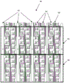
Fig. 3 shows a first embodiment of the invention. Fig. 3 illustrates that the touch sensor 40 of the first embodiment can arrange the sensing electrodes 42 as shown in the prior art. However, the arrangement of the drive electrodes 44 is changed. In particular, the first embodiment arranges a plurality of drive electrode pads 44 in a pseudo-random arrangement across the touch sensor 40 so that the touch sensor can be divided into different regions (also referred to as "touch sensor regions"), where each region can have a different arrangement of drive electrodes.
Having a different arrangement of drive electrodes 44 in each region may mean that the electric field generated in each region may be different due to the different arrangement of drive electrode pads 44 when the drive electrodes in touch sensor 40 receive a drive signal. For example, the arrangement of the driving electrode pad 44 in the first region may generate a strong electric field. In contrast, the arrangement of the drive electrode pad 44 in the second region may produce a weaker or substantially cancelled electric field. Such different arrangements of the drive electrode pads 44 in different regions may enable the different regions to operate independently of one another and/or reduce interference with one another.
One concept that should be made clear is what the drive or sense electrode pads are "different" from each other in the touch sensor area. For example, in FIG. 2, drive electrode pads d1 through d12 refer to different drive pins on the touch sensor controller. Thus, having different drive electrode pads for the touch sensor regions means that the signal sources to the drive electrode pads are different. Conversely, if there are multiple copies of a single drive electrode pad, this means that there are multiple drive electrode pads that are driven by the same signal source, e.g., the same drive pin (pin) on the touch sensor controller. Likewise, the same concept can be applied to the sense drive pads and pins transmitted to the touch sensor controller.
Fig. 3 shows an example of 12 drive electrode pads 44, labeled d1 through d12, arranged in a pseudo-virtual pattern defining first regions 46 and second regions 48, as indicated by the dashed boxes. The number of regions is not limited to two. There may be additional distinct regions above, below, to the right, or to the left of the two regions 46, 48 shown. The other regions may have a different arrangement of drive electrode pads 44 than the first or second regions 46, 48, or one or both of these regions may be repeated as desired.
It will be appreciated that the particular arrangement of the drive electrode pad 44 may be modified without departing from embodiments of the invention. Further, it should be understood that the path traces 50 may continue above and below the particular arrangement of electrodes shown to build a larger touch sensor 40. It should be understood that the arrangement of the drive electrode pad 44 may be such that only one region, or more than one region, has a useful electric field at a time. The regions having a useful electric field may or may not be adjacent to each other.
A touch controller that generates a pattern of stimulation (pattern) delivered on the drive electrodes of the touch sensor 40 can select certain sets of drive electrode pads 44 to be driven at any given time so that each region can be activated by a strong electric field, either alone or in combination with other regions.
In another embodiment of the present invention, the phase of the drive signal transmitted to the drive electrode pad 44 may also be manipulated to affect the electric field in different regions. In this embodiment, a drive stimulation pattern may be transmitted from the touch controller such that some of the drive electrode pads 44 are driven by in-phase signals, while other drive electrodes may be driven by out-of-phase signals.
For example, all of the drive electrodes may be driven simultaneously. However, some of the drive electrodes receive signals that may be in phase, while the remaining drive electrodes receive signals that may be out of phase.
The result may be that during certain measurement operations, some areas of the touch sensor may have strong electric fields, where the acquisition (collection) of the drive electrodes are all in phase. Conversely, in other regions, which may have substantially the same mix of in-phase and out-of-phase drive electrodes, the net electric field may be very small. Still, other regions may have a mixture of in-phase drive electrodes more than out-of-phase drive electrodes, which may result in a less strong, but less weak, in-phase electric field. Similarly, if the regions have more mixing of out-of-phase drive electrodes than in-phase drive electrodes, the resulting electric field may be weaker than described above, but still have a useful electric field.
Thus, various stimulation patterns may be used to generate various electrical patterns with various intensity levels across the touch sensor and across multiple measurement cycles.
In one example that is achievable with regions having various levels of electric field strength, the analog-to-digital conversion (ADC) results for each sensing electrode per measurement can be a vector. The capacitance at each node can be determined by finding the dot product of each orthogonal vector. The result may be a capacitance magnitude image of the entire surface of the touch sensor.
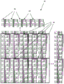
Fig. 4 shows another embodiment of the present invention. In this embodiment, there may be regions where one particular drive electrode pad 44 is repeated multiple times, such that, in effect, the repeated drive electrode pad occupies substantially more area in that same region than the other drive electrodes. The larger number of drive electrode pads 44 can be used as "limiters" for other drive electrodes in that particular region. In other words, a repeated drive electrode pad 44 may be driven by the same phase as other drive electrode pads 44 that are simply not repeated or repeated a lesser number of times in the same region. The effect may be to create a larger electric field for interaction with the finger for a particular measurement.
Other regions not of interest during a particular measurement may also have a repetitive electrode drive pad 44 that is driven. Although this may be undesirable, the generation of the electric field may be counteracted by the excited adjacent out-of-phase drive electrode pads, thereby cancelling the electric field in the region of the undesired electric field.
Thus, in fig. 4, first region 52 is shown with repeating electrode drive pad 44 labeled d 1. Thus, electrode drive pad d1 is the primary drive electrode pad 44 of first region 52. If electrode drive pad d1 is driven with a signal, this may restrict first region 52 as the region where touch measurements are being made. The second region 54 illustrates that the main electrode drive pad 44 is labeled d2, and thus d2 will be stimulated to make the second region 54 the primary region.
Fig. 5 shows another embodiment of the present invention. Instead of using a large sense electrode, which in the previous embodiment could be used by multiple regions, the sense electrode could be made up of multiple smaller sense electrode pads 60. One of the advantages is that sensing can be localized to a smaller area of the touch sensor 40, which can be given different functionality, much like the drive electrode pad 44. In this embodiment, the sense electrode pads 60 may be grouped into smaller regions on multiple shorter columns. The adjacent drive electrode pad 44 may be unique for each portion of the sense electrode. Dividing the sense electrodes into smaller electrodes may create a unique "addressing" for smaller areas of the touch sensor 40.
An advantage of this approach may be that the drive electrode pads 44 in each column may repeatedly increase the number of columns for each unique set of adjacent sense electrode pads 60, thereby enabling the creation of a large touch sensor 40.
It is noted that some of the sense electrode pads 60 may be routed from the bottom of the touch sensor 40, while others may be routed from the top of the touch sensor. In any of these embodiments, the function of the sense electrode pad 60 may also be swapped with the drive electrode pad 44, so either electrode pad may be the drive electrode pad 44 or the sense electrode pad 60 for any measurement.
The above-described embodiments demonstrate the versatility of not only being able to redistribute the electrode functions as needed, but also the ability to combine electrodes together to create larger and larger touch sensors by creating multiple regions that do not interfere with each other. In addition, the size of the regions may also vary.
In another aspect, different functions of adjacent regions may be assigned by using in-phase and out-of-phase drive signals, or different combinations of drive and sense electrode pads.
Fig. 5 shows various regions that may be created. By grouping a particular set of sense electrode pads 60 based on their association, different regions 66 are shown. FIG. 5 also shows that the regions extend to the top or bottom, left or right, as desired.
Embodiments of the invention may be directed to methods of reducing the path traces to a touch sensor by creating touch sensor areas of drive and sense electrode pads where different areas have different arrangements of drive and sense electrode pads.
The method may include first providing a touch sensor controller of a touch sensor for generating a drive signal, the drive signal being transmitted through a drive path trace to a drive electrode pad; and the touch sensor controller is to receive sense signals from the plurality of sense electrodes through the sense path traces. The method may further include forming touch sensor regions in the touch sensor, wherein adjacent touch sensor regions have different arrangements of sense electrode pads and drive electrode pads such that adjacent touch sensor regions do not generate electric fields that interfere with each other.
Although only a few exemplary embodiments have been described in detail above, those skilled in the art will readily appreciate that many modifications are possible in the exemplary embodiments without materially departing from this invention. Accordingly, all such modifications are intended to be included within the scope of this disclosure as defined in the following claims. It is not the intention of the applicant to restrict any one claim to article 6 of 35u.s.c. 112 except to the extent that the claim explicitly uses the word "means" and related functionality.
Claims (9)
1. A method of reducing the number of routing traces to a touch sensor by creating touch sensor regions of drive and sense electrode pads, wherein different regions have different arrangements of the drive and sense electrode pads, the method comprising:
a touch sensor controller providing the touch sensor for generating drive signals that are transmitted to the drive electrode pads through drive path traces, and for receiving sense signals from a plurality of sense electrodes through sense path traces; and
forming touch sensor regions in the touch sensor, wherein adjacent touch sensor regions have different arrangements of the sensing electrode pads and the driving electrode pads such that the adjacent touch sensor regions do not generate electric fields that interfere with each other,
wherein the method further comprises driving selected ones of the plurality of drive electrode pads with a first signal that is in phase and driving different selected ones of the plurality of drive electrode pads with a second signal that is out of phase with the first signal to thereby vary the electric field generated in the touch sensor area.
2. The method of claim 1, further comprising disposing the sense electrode pad in an adjacent touch sensor region, the sense electrode pad being transmitted to one input of the touch sensor controller.
3. The method of claim 1, further comprising not arranging the same sense electrode pad in adjacent touch sensor regions, the sense electrode pad being transmitted to one input of the touch sensor controller.
4. The method of claim 1, wherein the method further comprises providing multiple copies of touch sensor regions having a particular arrangement of the sense electrode pads and the drive electrode pads on the same row of touch sensor regions within the touch sensor, so long as the copies are not adjacent to each other.
5. The method of claim 4, wherein the method further comprises providing multiple copies of the touch sensor regions having a particular arrangement of the sense electrode pads and the drive electrode pads on the same column of touch sensor regions within the touch sensor, so long as the copies are not adjacent to each other on the same column or the same row.
6. The method of claim 1, wherein the method further comprises transmitting the drive signal to the drive electrode pads that will generate a strong electric field in a first touch sensor region, while the same drive signal will generate a weak electric field in a second touch sensor region adjacent to the first touch sensor region because the arrangement of the drive electrode pads is different in the first and second touch sensor regions.
7. The method of claim 1, wherein the method further comprises the step of transmitting some in-phase and out-of-phase drive signals to the same touch sensor area to thereby vary the strength of the electric field generated within the touch sensor area.
8. The method of claim 1, wherein the method further comprises:
providing multiple copies of a single sense electrode pad in each of the touch sensor regions; and
a plurality of different drive electrode pads are provided within each of the touch sensor regions.
9. The method of claim 1, further comprising providing a plurality of different drive electrode pads in each of the touch sensor regions, and providing multiple copies of one drive electrode pad, such that the one drive electrode pad dominates each of the plurality of touch sensor regions because of the number of copies of the drive electrode pad disposed within the touch sensor region.
Applications Claiming Priority (3)
| Application Number | Priority Date | Filing Date | Title |
|---|---|---|---|
| US201562130796P | 2015-03-10 | 2015-03-10 | |
| US62/130,796 | 2015-03-10 | ||
| PCT/US2016/021823 WO2016145224A1 (en) | 2015-03-10 | 2016-03-10 | Method of reducing electrode routing on single layer touch sensor |
Publications (2)
| Publication Number | Publication Date |
|---|---|
| CN107430468A CN107430468A (en) | 2017-12-01 |
| CN107430468B true CN107430468B (en) | 2020-10-16 |
Family
ID=56880597
Family Applications (1)
| Application Number | Title | Priority Date | Filing Date |
|---|---|---|---|
| CN201680015110.2A Expired - Fee Related CN107430468B (en) | 2015-03-10 | 2016-03-10 | Method for reducing electrode paths on a single layer touch sensor |
Country Status (4)
| Country | Link |
|---|---|
| US (1) | US10152163B2 (en) |
| JP (1) | JP6757327B2 (en) |
| CN (1) | CN107430468B (en) |
| WO (1) | WO2016145224A1 (en) |
Families Citing this family (7)
| Publication number | Priority date | Publication date | Assignee | Title |
|---|---|---|---|---|
| CN104793825B (en) * | 2015-04-30 | 2018-04-20 | 京东方科技集团股份有限公司 | A kind of touch input equipment and touch display device |
| DE112018004416T5 (en) | 2017-10-03 | 2020-05-20 | Wacom Co., Ltd. | SENSOR PANEL FOR DETECTING A PEN SIGNAL SENT FROM A PEN |
| WO2019116754A1 (en) * | 2017-12-13 | 2019-06-20 | 富士フイルム株式会社 | Conductive member, touch panel, and display device |
| CN109976567B (en) * | 2018-03-26 | 2020-08-04 | 京东方科技集团股份有限公司 | Touch panel, driving method thereof and touch device |
| KR102336301B1 (en) * | 2018-08-03 | 2021-12-09 | 주식회사 하이딥 | Touch sensor panel and touch input apparatus |
| US10817111B1 (en) * | 2019-04-10 | 2020-10-27 | Semiconductor Components Industries, Llc | Methods and apparatus for a capacitive touch sensor |
| KR102259904B1 (en) * | 2019-11-27 | 2021-06-03 | 주식회사 하이딥 | Touch input device |
Citations (8)
| Publication number | Priority date | Publication date | Assignee | Title |
|---|---|---|---|---|
| CN101566895A (en) * | 2008-04-25 | 2009-10-28 | 苹果公司 | Brick layout and stackup for touch screen |
| CN102591519A (en) * | 2010-12-02 | 2012-07-18 | 爱特梅尔公司 | Position-sensing and force detection panel |
| CN102799329A (en) * | 2012-07-25 | 2012-11-28 | 东莞市乐升电子有限公司 | Projected capacitive touch screen panel with single-layer indium tin compound electrode |
| CN103064553A (en) * | 2011-10-20 | 2013-04-24 | 爱特梅尔公司 | Single-layer touch sensor |
| CN103105991A (en) * | 2013-01-25 | 2013-05-15 | 深圳市汇顶科技股份有限公司 | Monolayer capacitance touch sensor and touch control terminal |
| CN103460161A (en) * | 2011-04-01 | 2013-12-18 | 麦孚斯公司 | Apparatus and method for detecting contact |
| WO2013188307A2 (en) * | 2012-06-12 | 2013-12-19 | Yknots Industries Llc | Haptic electromagnetic actuator |
| CN104281327A (en) * | 2014-10-29 | 2015-01-14 | 合肥鑫晟光电科技有限公司 | Touch screen and manufacturing method and display device thereof |
Family Cites Families (23)
| Publication number | Priority date | Publication date | Assignee | Title |
|---|---|---|---|---|
| CN101673162A (en) | 2008-04-10 | 2010-03-17 | 爱特梅尔公司 | Capacitive touch sensor with noise inhibition |
| US9041682B2 (en) * | 2009-10-23 | 2015-05-26 | Atmel Corporation | Driving electrodes with different phase signals |
| CN102200866B (en) * | 2010-03-24 | 2015-11-25 | 上海天马微电子有限公司 | Mutual capacitance touch induction installation and detection method, touch display unit |
| TW201214252A (en) | 2010-09-24 | 2012-04-01 | Elan Microelectronics Corp | Two-dimensional single-layer implemented touch pad |
| EP2538313B1 (en) * | 2011-06-20 | 2015-05-20 | Melfas, Inc. | Touch sensor panel |
| US9632629B2 (en) * | 2011-09-29 | 2017-04-25 | Parade Technologies, Ltd. | Sensor patterns with reduced noise coupling |
| US20130081869A1 (en) * | 2011-09-30 | 2013-04-04 | Jae Hong Kim | Touch sensing apparatus and method of manufacturing the same |
| CN107256104B (en) * | 2012-01-12 | 2020-03-20 | 辛纳普蒂克斯公司 | Single-layer capacitive image sensor |
| US8910104B2 (en) | 2012-01-23 | 2014-12-09 | Cirque Corporation | Graduated routing for routing electrodes coupled to touch sensor electrodes to thereby balance capacitance on the touch sensor electrodes |
| CN103164091A (en) * | 2012-08-31 | 2013-06-19 | 敦泰科技有限公司 | Single-layer electrode mutual capacitance touch screen |
| US9360972B1 (en) | 2013-01-14 | 2016-06-07 | Cypress Semiconductor Corporation | Touch sensor conductor routing |
| US9292138B2 (en) * | 2013-02-08 | 2016-03-22 | Parade Technologies, Ltd. | Single layer sensor pattern |
| TWI537652B (en) * | 2013-03-01 | 2016-06-11 | 奕力科技股份有限公司 | Capacitive touch device with single electrode layer and panel module thereof |
| US9231588B2 (en) | 2013-04-30 | 2016-01-05 | Atmel Corporation | Touchscreen routing flow for single layer pattern |
| KR102044476B1 (en) * | 2013-05-02 | 2019-11-13 | 삼성전자주식회사 | Touch screen panel, touch senssing controller and touch sensing system comprising the same |
| CN104346004B (en) * | 2013-07-29 | 2017-08-29 | 原相科技股份有限公司 | Single-layer capacitive touch sensor |
| US9495046B2 (en) * | 2013-10-23 | 2016-11-15 | Synaptics Incorporated | Parasitic capacitance filter for single-layer capacitive imaging sensors |
| US9081457B2 (en) * | 2013-10-30 | 2015-07-14 | Synaptics Incorporated | Single-layer muti-touch capacitive imaging sensor |
| TWI546721B (en) * | 2014-07-25 | 2016-08-21 | 聯詠科技股份有限公司 | Touch panel and method for arranging electrode thereof |
| TWI539355B (en) * | 2014-10-28 | 2016-06-21 | 群創光電股份有限公司 | Touch control display apparatus and touch display detection method thereof |
| US9563319B2 (en) * | 2014-12-18 | 2017-02-07 | Synaptics Incorporated | Capacitive sensing without a baseline |
| KR102349436B1 (en) * | 2015-01-06 | 2022-01-10 | 삼성디스플레이 주식회사 | Touch sensor device and display device comprising the same |
| KR102291564B1 (en) * | 2015-01-06 | 2021-08-19 | 삼성디스플레이 주식회사 | Touch panel comprising touch sensor and diriving method thereof |
-
2016
- 2016-03-10 JP JP2017547467A patent/JP6757327B2/en active Active
- 2016-03-10 US US15/066,875 patent/US10152163B2/en active Active
- 2016-03-10 WO PCT/US2016/021823 patent/WO2016145224A1/en active Application Filing
- 2016-03-10 CN CN201680015110.2A patent/CN107430468B/en not_active Expired - Fee Related
Patent Citations (8)
| Publication number | Priority date | Publication date | Assignee | Title |
|---|---|---|---|---|
| CN101566895A (en) * | 2008-04-25 | 2009-10-28 | 苹果公司 | Brick layout and stackup for touch screen |
| CN102591519A (en) * | 2010-12-02 | 2012-07-18 | 爱特梅尔公司 | Position-sensing and force detection panel |
| CN103460161A (en) * | 2011-04-01 | 2013-12-18 | 麦孚斯公司 | Apparatus and method for detecting contact |
| CN103064553A (en) * | 2011-10-20 | 2013-04-24 | 爱特梅尔公司 | Single-layer touch sensor |
| WO2013188307A2 (en) * | 2012-06-12 | 2013-12-19 | Yknots Industries Llc | Haptic electromagnetic actuator |
| CN102799329A (en) * | 2012-07-25 | 2012-11-28 | 东莞市乐升电子有限公司 | Projected capacitive touch screen panel with single-layer indium tin compound electrode |
| CN103105991A (en) * | 2013-01-25 | 2013-05-15 | 深圳市汇顶科技股份有限公司 | Monolayer capacitance touch sensor and touch control terminal |
| CN104281327A (en) * | 2014-10-29 | 2015-01-14 | 合肥鑫晟光电科技有限公司 | Touch screen and manufacturing method and display device thereof |
Also Published As
| Publication number | Publication date |
|---|---|
| US20160266710A1 (en) | 2016-09-15 |
| US10152163B2 (en) | 2018-12-11 |
| JP6757327B2 (en) | 2020-09-16 |
| CN107430468A (en) | 2017-12-01 |
| WO2016145224A1 (en) | 2016-09-15 |
| JP2018508079A (en) | 2018-03-22 |
Similar Documents
| Publication | Publication Date | Title |
|---|---|---|
| CN107430468B (en) | Method for reducing electrode paths on a single layer touch sensor | |
| US9760226B2 (en) | Linear projected single-layer capacitance sensor | |
| CN106203250B (en) | Fingerprint sensor integrated-type touch screen panel | |
| KR101606015B1 (en) | Input device based on voltage gradients | |
| US9292115B2 (en) | Apparatus and method for detecting user input | |
| EP3291067B1 (en) | Touch control input device and touch display device | |
| US9391610B2 (en) | Single layer touchscreen with ground insertion | |
| US11473938B2 (en) | Enhancing sensitivity and robustness of mechanical rotation and position detection with capacitive sensors | |
| US20150062075A1 (en) | Capacitive input device | |
| US20140111474A1 (en) | Multiplexed conductors using dynamically configurable controller in capacitive touch sensors | |
| CN102541369A (en) | Capacitive touch panel | |
| CN107250957B (en) | Touch panel and touch panel device | |
| US20120026131A1 (en) | Reducing noise susceptibility in a mutual capacitance touchpad through axis swapping | |
| US9572263B2 (en) | Graduated routing for electrodes coupled to touch sensor electrodes | |
| CN104238835B (en) | Contact panel and its touch electrode structure and method for detecting | |
| US20150077390A1 (en) | Touch panel input device and input detection method thereof | |
| JP6387390B2 (en) | Multiplexing and decomposing to reduce drive and sense electrodes of single layer touch sensors | |
| TWI536231B (en) | Multi-touch detection method and device thereof | |
| CN110730943A (en) | Position detection sensor, position detection device, and information processing system | |
| US20170046005A1 (en) | Avoiding noise when using multiple capacitive measuring integrated circuits | |
| KR101372329B1 (en) | Driving electrode pattern, touch panel, touch panel module, and electric device including the same | |
| US9086765B2 (en) | Interdigitated randomized electrode pattern to increase the area of a touchpad having a limited number of controller IC drive pins | |
| KR20130102024A (en) | Driving electrode pattern, touch panel, touch panel module, and electric device including the same | |
| US20240102871A1 (en) | Force Input Localisation | |
| US20110084920A1 (en) | Reducing layers in a touchpad by maximizing distance between a ground plane and sensor electrodes electrodes |
Legal Events
| Date | Code | Title | Description |
|---|---|---|---|
| PB01 | Publication | ||
| PB01 | Publication | ||
| SE01 | Entry into force of request for substantive examination | ||
| SE01 | Entry into force of request for substantive examination | ||
| GR01 | Patent grant | ||
| GR01 | Patent grant | ||
| CF01 | Termination of patent right due to non-payment of annual fee |
Granted publication date: 20201016 |
|
| CF01 | Termination of patent right due to non-payment of annual fee |