CN107408490B - Method for producing a semiconductor wafer with distributed doping and wafer comprising a distributed field - Google Patents
Method for producing a semiconductor wafer with distributed doping and wafer comprising a distributed field Download PDFInfo
- Publication number
- CN107408490B CN107408490B CN201580078308.0A CN201580078308A CN107408490B CN 107408490 B CN107408490 B CN 107408490B CN 201580078308 A CN201580078308 A CN 201580078308A CN 107408490 B CN107408490 B CN 107408490B
- Authority
- CN
- China
- Prior art keywords
- wafer
- dopant
- concentration
- semiconductor
- mold
- Prior art date
- Legal status (The legal status is an assumption and is not a legal conclusion. Google has not performed a legal analysis and makes no representation as to the accuracy of the status listed.)
- Active
Links
- 239000004065 semiconductor Substances 0.000 title claims abstract description 149
- 238000004519 manufacturing process Methods 0.000 title description 9
- 239000002019 doping agent Substances 0.000 claims abstract description 341
- 239000000155 melt Substances 0.000 claims abstract description 100
- 230000003287 optical effect Effects 0.000 claims abstract description 17
- 239000004020 conductor Substances 0.000 claims abstract description 12
- 235000012431 wafers Nutrition 0.000 claims description 340
- 238000000034 method Methods 0.000 claims description 106
- 229910052796 boron Inorganic materials 0.000 claims description 98
- ZOXJGFHDIHLPTG-UHFFFAOYSA-N Boron Chemical compound [B] ZOXJGFHDIHLPTG-UHFFFAOYSA-N 0.000 claims description 96
- 239000002800 charge carrier Substances 0.000 claims description 60
- 239000000370 acceptor Substances 0.000 claims description 56
- 239000000463 material Substances 0.000 claims description 53
- 229910052710 silicon Inorganic materials 0.000 claims description 52
- 238000005204 segregation Methods 0.000 claims description 51
- 239000010703 silicon Substances 0.000 claims description 49
- 229910052782 aluminium Inorganic materials 0.000 claims description 36
- XAGFODPZIPBFFR-UHFFFAOYSA-N aluminium Chemical compound [Al] XAGFODPZIPBFFR-UHFFFAOYSA-N 0.000 claims description 35
- 229910052698 phosphorus Inorganic materials 0.000 claims description 33
- OAICVXFJPJFONN-UHFFFAOYSA-N Phosphorus Chemical compound [P] OAICVXFJPJFONN-UHFFFAOYSA-N 0.000 claims description 29
- 230000005684 electric field Effects 0.000 claims description 28
- 239000011574 phosphorus Substances 0.000 claims description 28
- 238000000576 coating method Methods 0.000 claims description 27
- 229910052733 gallium Inorganic materials 0.000 claims description 27
- GYHNNYVSQQEPJS-UHFFFAOYSA-N Gallium Chemical compound [Ga] GYHNNYVSQQEPJS-UHFFFAOYSA-N 0.000 claims description 26
- 239000011248 coating agent Substances 0.000 claims description 26
- 239000012535 impurity Substances 0.000 claims description 26
- 229910052738 indium Inorganic materials 0.000 claims description 21
- APFVFJFRJDLVQX-UHFFFAOYSA-N indium atom Chemical compound [In] APFVFJFRJDLVQX-UHFFFAOYSA-N 0.000 claims description 19
- 229910052751 metal Inorganic materials 0.000 claims description 17
- 239000002184 metal Substances 0.000 claims description 17
- 229910052785 arsenic Inorganic materials 0.000 claims description 16
- 229910052797 bismuth Inorganic materials 0.000 claims description 16
- 229910052787 antimony Inorganic materials 0.000 claims description 15
- RQNWIZPPADIBDY-UHFFFAOYSA-N arsenic atom Chemical compound [As] RQNWIZPPADIBDY-UHFFFAOYSA-N 0.000 claims description 14
- JCXGWMGPZLAOME-UHFFFAOYSA-N bismuth atom Chemical compound [Bi] JCXGWMGPZLAOME-UHFFFAOYSA-N 0.000 claims description 14
- WATWJIUSRGPENY-UHFFFAOYSA-N antimony atom Chemical compound [Sb] WATWJIUSRGPENY-UHFFFAOYSA-N 0.000 claims description 13
- 150000001875 compounds Chemical class 0.000 claims description 9
- 238000007493 shaping process Methods 0.000 claims description 9
- 230000007704 transition Effects 0.000 claims description 8
- -1 oxides Chemical class 0.000 claims description 3
- 229910021332 silicide Inorganic materials 0.000 claims description 3
- 150000001247 metal acetylides Chemical class 0.000 claims description 2
- 150000004767 nitrides Chemical class 0.000 claims description 2
- 239000007787 solid Substances 0.000 abstract description 8
- 230000007423 decrease Effects 0.000 abstract 1
- 210000004027 cell Anatomy 0.000 description 53
- XUIMIQQOPSSXEZ-UHFFFAOYSA-N Silicon Chemical compound [Si] XUIMIQQOPSSXEZ-UHFFFAOYSA-N 0.000 description 45
- 239000010410 layer Substances 0.000 description 20
- 239000012768 molten material Substances 0.000 description 19
- 238000009792 diffusion process Methods 0.000 description 17
- 230000012010 growth Effects 0.000 description 17
- 239000000969 carrier Substances 0.000 description 15
- 239000013078 crystal Substances 0.000 description 10
- 230000008569 process Effects 0.000 description 10
- 238000007711 solidification Methods 0.000 description 10
- 230000008023 solidification Effects 0.000 description 10
- 230000008901 benefit Effects 0.000 description 9
- 230000000694 effects Effects 0.000 description 9
- 229910052580 B4C Inorganic materials 0.000 description 7
- 229910052582 BN Inorganic materials 0.000 description 7
- PZNSFCLAULLKQX-UHFFFAOYSA-N Boron nitride Chemical compound N#B PZNSFCLAULLKQX-UHFFFAOYSA-N 0.000 description 7
- 238000009825 accumulation Methods 0.000 description 7
- 230000015572 biosynthetic process Effects 0.000 description 7
- INAHAJYZKVIDIZ-UHFFFAOYSA-N boron carbide Chemical compound B12B3B4C32B41 INAHAJYZKVIDIZ-UHFFFAOYSA-N 0.000 description 7
- 238000012545 processing Methods 0.000 description 7
- 239000000758 substrate Substances 0.000 description 6
- 229910000838 Al alloy Inorganic materials 0.000 description 5
- 230000009286 beneficial effect Effects 0.000 description 5
- 229910052810 boron oxide Inorganic materials 0.000 description 5
- 238000001816 cooling Methods 0.000 description 5
- JKWMSGQKBLHBQQ-UHFFFAOYSA-N diboron trioxide Chemical compound O=BOB=O JKWMSGQKBLHBQQ-UHFFFAOYSA-N 0.000 description 5
- 239000011148 porous material Substances 0.000 description 5
- 238000013459 approach Methods 0.000 description 4
- 125000004429 atom Chemical group 0.000 description 4
- 238000001704 evaporation Methods 0.000 description 4
- 230000008020 evaporation Effects 0.000 description 4
- 230000006870 function Effects 0.000 description 4
- 229910052732 germanium Inorganic materials 0.000 description 4
- GNPVGFCGXDBREM-UHFFFAOYSA-N germanium atom Chemical compound [Ge] GNPVGFCGXDBREM-UHFFFAOYSA-N 0.000 description 4
- 230000004888 barrier function Effects 0.000 description 3
- KGBXLFKZBHKPEV-UHFFFAOYSA-N boric acid Chemical compound OB(O)O KGBXLFKZBHKPEV-UHFFFAOYSA-N 0.000 description 3
- 239000004327 boric acid Substances 0.000 description 3
- 150000001639 boron compounds Chemical class 0.000 description 3
- 239000005388 borosilicate glass Substances 0.000 description 3
- 230000000875 corresponding effect Effects 0.000 description 3
- 239000007788 liquid Substances 0.000 description 3
- 230000007246 mechanism Effects 0.000 description 3
- 230000004048 modification Effects 0.000 description 3
- 238000012986 modification Methods 0.000 description 3
- 230000009467 reduction Effects 0.000 description 3
- 101001073212 Arabidopsis thaliana Peroxidase 33 Proteins 0.000 description 2
- JBRZTFJDHDCESZ-UHFFFAOYSA-N AsGa Chemical compound [As]#[Ga] JBRZTFJDHDCESZ-UHFFFAOYSA-N 0.000 description 2
- 101001123325 Homo sapiens Peroxisome proliferator-activated receptor gamma coactivator 1-beta Proteins 0.000 description 2
- GPXJNWSHGFTCBW-UHFFFAOYSA-N Indium phosphide Chemical compound [In]#P GPXJNWSHGFTCBW-UHFFFAOYSA-N 0.000 description 2
- 102100028961 Peroxisome proliferator-activated receptor gamma coactivator 1-beta Human genes 0.000 description 2
- 229910000676 Si alloy Inorganic materials 0.000 description 2
- CSDREXVUYHZDNP-UHFFFAOYSA-N alumanylidynesilicon Chemical compound [Al].[Si] CSDREXVUYHZDNP-UHFFFAOYSA-N 0.000 description 2
- 239000011449 brick Substances 0.000 description 2
- 229910052799 carbon Inorganic materials 0.000 description 2
- 238000004090 dissolution Methods 0.000 description 2
- 238000005516 engineering process Methods 0.000 description 2
- 230000004907 flux Effects 0.000 description 2
- 230000012447 hatching Effects 0.000 description 2
- 230000001771 impaired effect Effects 0.000 description 2
- 239000000203 mixture Substances 0.000 description 2
- 230000006911 nucleation Effects 0.000 description 2
- 238000010899 nucleation Methods 0.000 description 2
- 239000002245 particle Substances 0.000 description 2
- 230000000737 periodic effect Effects 0.000 description 2
- 230000006798 recombination Effects 0.000 description 2
- 238000005215 recombination Methods 0.000 description 2
- 230000004044 response Effects 0.000 description 2
- 229910001218 Gallium arsenide Inorganic materials 0.000 description 1
- XEEYBQQBJWHFJM-UHFFFAOYSA-N Iron Chemical compound [Fe] XEEYBQQBJWHFJM-UHFFFAOYSA-N 0.000 description 1
- 229910052581 Si3N4 Inorganic materials 0.000 description 1
- 229910003685 SiB4 Inorganic materials 0.000 description 1
- 229910052770 Uranium Inorganic materials 0.000 description 1
- 239000000654 additive Substances 0.000 description 1
- 239000004411 aluminium Substances 0.000 description 1
- 230000003698 anagen phase Effects 0.000 description 1
- 238000004458 analytical method Methods 0.000 description 1
- 230000005540 biological transmission Effects 0.000 description 1
- 210000003850 cellular structure Anatomy 0.000 description 1
- 229910052681 coesite Inorganic materials 0.000 description 1
- 239000008139 complexing agent Substances 0.000 description 1
- 239000000470 constituent Substances 0.000 description 1
- 230000002596 correlated effect Effects 0.000 description 1
- 229910052906 cristobalite Inorganic materials 0.000 description 1
- 229910021419 crystalline silicon Inorganic materials 0.000 description 1
- 238000005520 cutting process Methods 0.000 description 1
- 230000001627 detrimental effect Effects 0.000 description 1
- 238000007607 die coating method Methods 0.000 description 1
- 230000005496 eutectics Effects 0.000 description 1
- 230000001747 exhibiting effect Effects 0.000 description 1
- 238000000605 extraction Methods 0.000 description 1
- 238000010304 firing Methods 0.000 description 1
- 239000011888 foil Substances 0.000 description 1
- 230000004927 fusion Effects 0.000 description 1
- 239000007791 liquid phase Substances 0.000 description 1
- 238000005259 measurement Methods 0.000 description 1
- 239000007769 metal material Substances 0.000 description 1
- 229910052757 nitrogen Inorganic materials 0.000 description 1
- 238000001579 optical reflectometry Methods 0.000 description 1
- 229910052760 oxygen Inorganic materials 0.000 description 1
- 238000004806 packaging method and process Methods 0.000 description 1
- 238000002161 passivation Methods 0.000 description 1
- 125000004437 phosphorous atom Chemical group 0.000 description 1
- 238000002360 preparation method Methods 0.000 description 1
- 238000007712 rapid solidification Methods 0.000 description 1
- 230000009257 reactivity Effects 0.000 description 1
- 238000002310 reflectometry Methods 0.000 description 1
- 230000004043 responsiveness Effects 0.000 description 1
- 229920006395 saturated elastomer Polymers 0.000 description 1
- 230000035945 sensitivity Effects 0.000 description 1
- FVBUAEGBCNSCDD-UHFFFAOYSA-N silicide(4-) Chemical compound [Si-4] FVBUAEGBCNSCDD-UHFFFAOYSA-N 0.000 description 1
- 239000000377 silicon dioxide Substances 0.000 description 1
- VYPSYNLAJGMNEJ-UHFFFAOYSA-N silicon dioxide Inorganic materials O=[Si]=O VYPSYNLAJGMNEJ-UHFFFAOYSA-N 0.000 description 1
- 239000011343 solid material Substances 0.000 description 1
- 239000007790 solid phase Substances 0.000 description 1
- 230000003595 spectral effect Effects 0.000 description 1
- 229910052682 stishovite Inorganic materials 0.000 description 1
- 239000002344 surface layer Substances 0.000 description 1
- 230000001988 toxicity Effects 0.000 description 1
- 231100000419 toxicity Toxicity 0.000 description 1
- 229910052905 tridymite Inorganic materials 0.000 description 1
Images


Classifications
-
- H—ELECTRICITY
- H01—ELECTRIC ELEMENTS
- H01L—SEMICONDUCTOR DEVICES NOT COVERED BY CLASS H10
- H01L31/00—Semiconductor devices sensitive to infrared radiation, light, electromagnetic radiation of shorter wavelength or corpuscular radiation and specially adapted either for the conversion of the energy of such radiation into electrical energy or for the control of electrical energy by such radiation; Processes or apparatus specially adapted for the manufacture or treatment thereof or of parts thereof; Details thereof
- H01L31/18—Processes or apparatus specially adapted for the manufacture or treatment of these devices or of parts thereof
- H01L31/1804—Processes or apparatus specially adapted for the manufacture or treatment of these devices or of parts thereof comprising only elements of Group IV of the Periodic System
-
- H—ELECTRICITY
- H01—ELECTRIC ELEMENTS
- H01L—SEMICONDUCTOR DEVICES NOT COVERED BY CLASS H10
- H01L31/00—Semiconductor devices sensitive to infrared radiation, light, electromagnetic radiation of shorter wavelength or corpuscular radiation and specially adapted either for the conversion of the energy of such radiation into electrical energy or for the control of electrical energy by such radiation; Processes or apparatus specially adapted for the manufacture or treatment thereof or of parts thereof; Details thereof
- H01L31/18—Processes or apparatus specially adapted for the manufacture or treatment of these devices or of parts thereof
-
- C—CHEMISTRY; METALLURGY
- C30—CRYSTAL GROWTH
- C30B—SINGLE-CRYSTAL GROWTH; UNIDIRECTIONAL SOLIDIFICATION OF EUTECTIC MATERIAL OR UNIDIRECTIONAL DEMIXING OF EUTECTOID MATERIAL; REFINING BY ZONE-MELTING OF MATERIAL; PRODUCTION OF A HOMOGENEOUS POLYCRYSTALLINE MATERIAL WITH DEFINED STRUCTURE; SINGLE CRYSTALS OR HOMOGENEOUS POLYCRYSTALLINE MATERIAL WITH DEFINED STRUCTURE; AFTER-TREATMENT OF SINGLE CRYSTALS OR A HOMOGENEOUS POLYCRYSTALLINE MATERIAL WITH DEFINED STRUCTURE; APPARATUS THEREFOR
- C30B11/00—Single-crystal growth by normal freezing or freezing under temperature gradient, e.g. Bridgman-Stockbarger method
- C30B11/002—Crucibles or containers for supporting the melt
-
- C—CHEMISTRY; METALLURGY
- C30—CRYSTAL GROWTH
- C30B—SINGLE-CRYSTAL GROWTH; UNIDIRECTIONAL SOLIDIFICATION OF EUTECTIC MATERIAL OR UNIDIRECTIONAL DEMIXING OF EUTECTOID MATERIAL; REFINING BY ZONE-MELTING OF MATERIAL; PRODUCTION OF A HOMOGENEOUS POLYCRYSTALLINE MATERIAL WITH DEFINED STRUCTURE; SINGLE CRYSTALS OR HOMOGENEOUS POLYCRYSTALLINE MATERIAL WITH DEFINED STRUCTURE; AFTER-TREATMENT OF SINGLE CRYSTALS OR A HOMOGENEOUS POLYCRYSTALLINE MATERIAL WITH DEFINED STRUCTURE; APPARATUS THEREFOR
- C30B19/00—Liquid-phase epitaxial-layer growth
- C30B19/12—Liquid-phase epitaxial-layer growth characterised by the substrate
-
- C—CHEMISTRY; METALLURGY
- C30—CRYSTAL GROWTH
- C30B—SINGLE-CRYSTAL GROWTH; UNIDIRECTIONAL SOLIDIFICATION OF EUTECTIC MATERIAL OR UNIDIRECTIONAL DEMIXING OF EUTECTOID MATERIAL; REFINING BY ZONE-MELTING OF MATERIAL; PRODUCTION OF A HOMOGENEOUS POLYCRYSTALLINE MATERIAL WITH DEFINED STRUCTURE; SINGLE CRYSTALS OR HOMOGENEOUS POLYCRYSTALLINE MATERIAL WITH DEFINED STRUCTURE; AFTER-TREATMENT OF SINGLE CRYSTALS OR A HOMOGENEOUS POLYCRYSTALLINE MATERIAL WITH DEFINED STRUCTURE; APPARATUS THEREFOR
- C30B28/00—Production of homogeneous polycrystalline material with defined structure
- C30B28/04—Production of homogeneous polycrystalline material with defined structure from liquids
-
- C—CHEMISTRY; METALLURGY
- C30—CRYSTAL GROWTH
- C30B—SINGLE-CRYSTAL GROWTH; UNIDIRECTIONAL SOLIDIFICATION OF EUTECTIC MATERIAL OR UNIDIRECTIONAL DEMIXING OF EUTECTOID MATERIAL; REFINING BY ZONE-MELTING OF MATERIAL; PRODUCTION OF A HOMOGENEOUS POLYCRYSTALLINE MATERIAL WITH DEFINED STRUCTURE; SINGLE CRYSTALS OR HOMOGENEOUS POLYCRYSTALLINE MATERIAL WITH DEFINED STRUCTURE; AFTER-TREATMENT OF SINGLE CRYSTALS OR A HOMOGENEOUS POLYCRYSTALLINE MATERIAL WITH DEFINED STRUCTURE; APPARATUS THEREFOR
- C30B29/00—Single crystals or homogeneous polycrystalline material with defined structure characterised by the material or by their shape
- C30B29/02—Elements
- C30B29/06—Silicon
-
- C—CHEMISTRY; METALLURGY
- C30—CRYSTAL GROWTH
- C30B—SINGLE-CRYSTAL GROWTH; UNIDIRECTIONAL SOLIDIFICATION OF EUTECTIC MATERIAL OR UNIDIRECTIONAL DEMIXING OF EUTECTOID MATERIAL; REFINING BY ZONE-MELTING OF MATERIAL; PRODUCTION OF A HOMOGENEOUS POLYCRYSTALLINE MATERIAL WITH DEFINED STRUCTURE; SINGLE CRYSTALS OR HOMOGENEOUS POLYCRYSTALLINE MATERIAL WITH DEFINED STRUCTURE; AFTER-TREATMENT OF SINGLE CRYSTALS OR A HOMOGENEOUS POLYCRYSTALLINE MATERIAL WITH DEFINED STRUCTURE; APPARATUS THEREFOR
- C30B31/00—Diffusion or doping processes for single crystals or homogeneous polycrystalline material with defined structure; Apparatus therefor
- C30B31/02—Diffusion or doping processes for single crystals or homogeneous polycrystalline material with defined structure; Apparatus therefor by contacting with diffusion materials in the solid state
-
- C—CHEMISTRY; METALLURGY
- C30—CRYSTAL GROWTH
- C30B—SINGLE-CRYSTAL GROWTH; UNIDIRECTIONAL SOLIDIFICATION OF EUTECTIC MATERIAL OR UNIDIRECTIONAL DEMIXING OF EUTECTOID MATERIAL; REFINING BY ZONE-MELTING OF MATERIAL; PRODUCTION OF A HOMOGENEOUS POLYCRYSTALLINE MATERIAL WITH DEFINED STRUCTURE; SINGLE CRYSTALS OR HOMOGENEOUS POLYCRYSTALLINE MATERIAL WITH DEFINED STRUCTURE; AFTER-TREATMENT OF SINGLE CRYSTALS OR A HOMOGENEOUS POLYCRYSTALLINE MATERIAL WITH DEFINED STRUCTURE; APPARATUS THEREFOR
- C30B31/00—Diffusion or doping processes for single crystals or homogeneous polycrystalline material with defined structure; Apparatus therefor
- C30B31/04—Diffusion or doping processes for single crystals or homogeneous polycrystalline material with defined structure; Apparatus therefor by contacting with diffusion materials in the liquid state
-
- C—CHEMISTRY; METALLURGY
- C30—CRYSTAL GROWTH
- C30B—SINGLE-CRYSTAL GROWTH; UNIDIRECTIONAL SOLIDIFICATION OF EUTECTIC MATERIAL OR UNIDIRECTIONAL DEMIXING OF EUTECTOID MATERIAL; REFINING BY ZONE-MELTING OF MATERIAL; PRODUCTION OF A HOMOGENEOUS POLYCRYSTALLINE MATERIAL WITH DEFINED STRUCTURE; SINGLE CRYSTALS OR HOMOGENEOUS POLYCRYSTALLINE MATERIAL WITH DEFINED STRUCTURE; AFTER-TREATMENT OF SINGLE CRYSTALS OR A HOMOGENEOUS POLYCRYSTALLINE MATERIAL WITH DEFINED STRUCTURE; APPARATUS THEREFOR
- C30B35/00—Apparatus not otherwise provided for, specially adapted for the growth, production or after-treatment of single crystals or of a homogeneous polycrystalline material with defined structure
- C30B35/002—Crucibles or containers
-
- H—ELECTRICITY
- H01—ELECTRIC ELEMENTS
- H01L—SEMICONDUCTOR DEVICES NOT COVERED BY CLASS H10
- H01L21/00—Processes or apparatus adapted for the manufacture or treatment of semiconductor or solid state devices or of parts thereof
-
- H—ELECTRICITY
- H01—ELECTRIC ELEMENTS
- H01L—SEMICONDUCTOR DEVICES NOT COVERED BY CLASS H10
- H01L31/00—Semiconductor devices sensitive to infrared radiation, light, electromagnetic radiation of shorter wavelength or corpuscular radiation and specially adapted either for the conversion of the energy of such radiation into electrical energy or for the control of electrical energy by such radiation; Processes or apparatus specially adapted for the manufacture or treatment thereof or of parts thereof; Details thereof
- H01L31/02—Details
- H01L31/0216—Coatings
- H01L31/02161—Coatings for devices characterised by at least one potential jump barrier or surface barrier
- H01L31/02167—Coatings for devices characterised by at least one potential jump barrier or surface barrier for solar cells
-
- H—ELECTRICITY
- H01—ELECTRIC ELEMENTS
- H01L—SEMICONDUCTOR DEVICES NOT COVERED BY CLASS H10
- H01L31/00—Semiconductor devices sensitive to infrared radiation, light, electromagnetic radiation of shorter wavelength or corpuscular radiation and specially adapted either for the conversion of the energy of such radiation into electrical energy or for the control of electrical energy by such radiation; Processes or apparatus specially adapted for the manufacture or treatment thereof or of parts thereof; Details thereof
- H01L31/02—Details
- H01L31/0224—Electrodes
- H01L31/022408—Electrodes for devices characterised by at least one potential jump barrier or surface barrier
- H01L31/022425—Electrodes for devices characterised by at least one potential jump barrier or surface barrier for solar cells
-
- H—ELECTRICITY
- H01—ELECTRIC ELEMENTS
- H01L—SEMICONDUCTOR DEVICES NOT COVERED BY CLASS H10
- H01L31/00—Semiconductor devices sensitive to infrared radiation, light, electromagnetic radiation of shorter wavelength or corpuscular radiation and specially adapted either for the conversion of the energy of such radiation into electrical energy or for the control of electrical energy by such radiation; Processes or apparatus specially adapted for the manufacture or treatment thereof or of parts thereof; Details thereof
- H01L31/0248—Semiconductor devices sensitive to infrared radiation, light, electromagnetic radiation of shorter wavelength or corpuscular radiation and specially adapted either for the conversion of the energy of such radiation into electrical energy or for the control of electrical energy by such radiation; Processes or apparatus specially adapted for the manufacture or treatment thereof or of parts thereof; Details thereof characterised by their semiconductor bodies
- H01L31/0256—Semiconductor devices sensitive to infrared radiation, light, electromagnetic radiation of shorter wavelength or corpuscular radiation and specially adapted either for the conversion of the energy of such radiation into electrical energy or for the control of electrical energy by such radiation; Processes or apparatus specially adapted for the manufacture or treatment thereof or of parts thereof; Details thereof characterised by their semiconductor bodies characterised by the material
- H01L31/0264—Inorganic materials
- H01L31/028—Inorganic materials including, apart from doping material or other impurities, only elements of Group IV of the Periodic System
- H01L31/0288—Inorganic materials including, apart from doping material or other impurities, only elements of Group IV of the Periodic System characterised by the doping material
-
- H—ELECTRICITY
- H01—ELECTRIC ELEMENTS
- H01L—SEMICONDUCTOR DEVICES NOT COVERED BY CLASS H10
- H01L31/00—Semiconductor devices sensitive to infrared radiation, light, electromagnetic radiation of shorter wavelength or corpuscular radiation and specially adapted either for the conversion of the energy of such radiation into electrical energy or for the control of electrical energy by such radiation; Processes or apparatus specially adapted for the manufacture or treatment thereof or of parts thereof; Details thereof
- H01L31/0248—Semiconductor devices sensitive to infrared radiation, light, electromagnetic radiation of shorter wavelength or corpuscular radiation and specially adapted either for the conversion of the energy of such radiation into electrical energy or for the control of electrical energy by such radiation; Processes or apparatus specially adapted for the manufacture or treatment thereof or of parts thereof; Details thereof characterised by their semiconductor bodies
- H01L31/0256—Semiconductor devices sensitive to infrared radiation, light, electromagnetic radiation of shorter wavelength or corpuscular radiation and specially adapted either for the conversion of the energy of such radiation into electrical energy or for the control of electrical energy by such radiation; Processes or apparatus specially adapted for the manufacture or treatment thereof or of parts thereof; Details thereof characterised by their semiconductor bodies characterised by the material
- H01L31/0264—Inorganic materials
- H01L31/0304—Inorganic materials including, apart from doping materials or other impurities, only AIIIBV compounds
- H01L31/03046—Inorganic materials including, apart from doping materials or other impurities, only AIIIBV compounds including ternary or quaternary compounds, e.g. GaAlAs, InGaAs, InGaAsP
-
- H—ELECTRICITY
- H01—ELECTRIC ELEMENTS
- H01L—SEMICONDUCTOR DEVICES NOT COVERED BY CLASS H10
- H01L31/00—Semiconductor devices sensitive to infrared radiation, light, electromagnetic radiation of shorter wavelength or corpuscular radiation and specially adapted either for the conversion of the energy of such radiation into electrical energy or for the control of electrical energy by such radiation; Processes or apparatus specially adapted for the manufacture or treatment thereof or of parts thereof; Details thereof
- H01L31/04—Semiconductor devices sensitive to infrared radiation, light, electromagnetic radiation of shorter wavelength or corpuscular radiation and specially adapted either for the conversion of the energy of such radiation into electrical energy or for the control of electrical energy by such radiation; Processes or apparatus specially adapted for the manufacture or treatment thereof or of parts thereof; Details thereof adapted as photovoltaic [PV] conversion devices
- H01L31/042—PV modules or arrays of single PV cells
- H01L31/048—Encapsulation of modules
-
- H—ELECTRICITY
- H01—ELECTRIC ELEMENTS
- H01L—SEMICONDUCTOR DEVICES NOT COVERED BY CLASS H10
- H01L31/00—Semiconductor devices sensitive to infrared radiation, light, electromagnetic radiation of shorter wavelength or corpuscular radiation and specially adapted either for the conversion of the energy of such radiation into electrical energy or for the control of electrical energy by such radiation; Processes or apparatus specially adapted for the manufacture or treatment thereof or of parts thereof; Details thereof
- H01L31/04—Semiconductor devices sensitive to infrared radiation, light, electromagnetic radiation of shorter wavelength or corpuscular radiation and specially adapted either for the conversion of the energy of such radiation into electrical energy or for the control of electrical energy by such radiation; Processes or apparatus specially adapted for the manufacture or treatment thereof or of parts thereof; Details thereof adapted as photovoltaic [PV] conversion devices
- H01L31/054—Optical elements directly associated or integrated with the PV cell, e.g. light-reflecting means or light-concentrating means
- H01L31/056—Optical elements directly associated or integrated with the PV cell, e.g. light-reflecting means or light-concentrating means the light-reflecting means being of the back surface reflector [BSR] type
-
- H—ELECTRICITY
- H01—ELECTRIC ELEMENTS
- H01L—SEMICONDUCTOR DEVICES NOT COVERED BY CLASS H10
- H01L31/00—Semiconductor devices sensitive to infrared radiation, light, electromagnetic radiation of shorter wavelength or corpuscular radiation and specially adapted either for the conversion of the energy of such radiation into electrical energy or for the control of electrical energy by such radiation; Processes or apparatus specially adapted for the manufacture or treatment thereof or of parts thereof; Details thereof
- H01L31/04—Semiconductor devices sensitive to infrared radiation, light, electromagnetic radiation of shorter wavelength or corpuscular radiation and specially adapted either for the conversion of the energy of such radiation into electrical energy or for the control of electrical energy by such radiation; Processes or apparatus specially adapted for the manufacture or treatment thereof or of parts thereof; Details thereof adapted as photovoltaic [PV] conversion devices
- H01L31/06—Semiconductor devices sensitive to infrared radiation, light, electromagnetic radiation of shorter wavelength or corpuscular radiation and specially adapted either for the conversion of the energy of such radiation into electrical energy or for the control of electrical energy by such radiation; Processes or apparatus specially adapted for the manufacture or treatment thereof or of parts thereof; Details thereof adapted as photovoltaic [PV] conversion devices characterised by at least one potential-jump barrier or surface barrier
- H01L31/068—Semiconductor devices sensitive to infrared radiation, light, electromagnetic radiation of shorter wavelength or corpuscular radiation and specially adapted either for the conversion of the energy of such radiation into electrical energy or for the control of electrical energy by such radiation; Processes or apparatus specially adapted for the manufacture or treatment thereof or of parts thereof; Details thereof adapted as photovoltaic [PV] conversion devices characterised by at least one potential-jump barrier or surface barrier the potential barriers being only of the PN homojunction type, e.g. bulk silicon PN homojunction solar cells or thin film polycrystalline silicon PN homojunction solar cells
-
- H—ELECTRICITY
- H01—ELECTRIC ELEMENTS
- H01L—SEMICONDUCTOR DEVICES NOT COVERED BY CLASS H10
- H01L31/00—Semiconductor devices sensitive to infrared radiation, light, electromagnetic radiation of shorter wavelength or corpuscular radiation and specially adapted either for the conversion of the energy of such radiation into electrical energy or for the control of electrical energy by such radiation; Processes or apparatus specially adapted for the manufacture or treatment thereof or of parts thereof; Details thereof
- H01L31/18—Processes or apparatus specially adapted for the manufacture or treatment of these devices or of parts thereof
- H01L31/1804—Processes or apparatus specially adapted for the manufacture or treatment of these devices or of parts thereof comprising only elements of Group IV of the Periodic System
- H01L31/182—Special manufacturing methods for polycrystalline Si, e.g. Si ribbon, poly Si ingots, thin films of polycrystalline Si
-
- Y—GENERAL TAGGING OF NEW TECHNOLOGICAL DEVELOPMENTS; GENERAL TAGGING OF CROSS-SECTIONAL TECHNOLOGIES SPANNING OVER SEVERAL SECTIONS OF THE IPC; TECHNICAL SUBJECTS COVERED BY FORMER USPC CROSS-REFERENCE ART COLLECTIONS [XRACs] AND DIGESTS
- Y02—TECHNOLOGIES OR APPLICATIONS FOR MITIGATION OR ADAPTATION AGAINST CLIMATE CHANGE
- Y02E—REDUCTION OF GREENHOUSE GAS [GHG] EMISSIONS, RELATED TO ENERGY GENERATION, TRANSMISSION OR DISTRIBUTION
- Y02E10/00—Energy generation through renewable energy sources
- Y02E10/50—Photovoltaic [PV] energy
- Y02E10/52—PV systems with concentrators
-
- Y—GENERAL TAGGING OF NEW TECHNOLOGICAL DEVELOPMENTS; GENERAL TAGGING OF CROSS-SECTIONAL TECHNOLOGIES SPANNING OVER SEVERAL SECTIONS OF THE IPC; TECHNICAL SUBJECTS COVERED BY FORMER USPC CROSS-REFERENCE ART COLLECTIONS [XRACs] AND DIGESTS
- Y02—TECHNOLOGIES OR APPLICATIONS FOR MITIGATION OR ADAPTATION AGAINST CLIMATE CHANGE
- Y02E—REDUCTION OF GREENHOUSE GAS [GHG] EMISSIONS, RELATED TO ENERGY GENERATION, TRANSMISSION OR DISTRIBUTION
- Y02E10/00—Energy generation through renewable energy sources
- Y02E10/50—Photovoltaic [PV] energy
- Y02E10/544—Solar cells from Group III-V materials
-
- Y—GENERAL TAGGING OF NEW TECHNOLOGICAL DEVELOPMENTS; GENERAL TAGGING OF CROSS-SECTIONAL TECHNOLOGIES SPANNING OVER SEVERAL SECTIONS OF THE IPC; TECHNICAL SUBJECTS COVERED BY FORMER USPC CROSS-REFERENCE ART COLLECTIONS [XRACs] AND DIGESTS
- Y02—TECHNOLOGIES OR APPLICATIONS FOR MITIGATION OR ADAPTATION AGAINST CLIMATE CHANGE
- Y02E—REDUCTION OF GREENHOUSE GAS [GHG] EMISSIONS, RELATED TO ENERGY GENERATION, TRANSMISSION OR DISTRIBUTION
- Y02E10/00—Energy generation through renewable energy sources
- Y02E10/50—Photovoltaic [PV] energy
- Y02E10/546—Polycrystalline silicon PV cells
-
- Y—GENERAL TAGGING OF NEW TECHNOLOGICAL DEVELOPMENTS; GENERAL TAGGING OF CROSS-SECTIONAL TECHNOLOGIES SPANNING OVER SEVERAL SECTIONS OF THE IPC; TECHNICAL SUBJECTS COVERED BY FORMER USPC CROSS-REFERENCE ART COLLECTIONS [XRACs] AND DIGESTS
- Y02—TECHNOLOGIES OR APPLICATIONS FOR MITIGATION OR ADAPTATION AGAINST CLIMATE CHANGE
- Y02E—REDUCTION OF GREENHOUSE GAS [GHG] EMISSIONS, RELATED TO ENERGY GENERATION, TRANSMISSION OR DISTRIBUTION
- Y02E10/00—Energy generation through renewable energy sources
- Y02E10/50—Photovoltaic [PV] energy
- Y02E10/547—Monocrystalline silicon PV cells
-
- Y—GENERAL TAGGING OF NEW TECHNOLOGICAL DEVELOPMENTS; GENERAL TAGGING OF CROSS-SECTIONAL TECHNOLOGIES SPANNING OVER SEVERAL SECTIONS OF THE IPC; TECHNICAL SUBJECTS COVERED BY FORMER USPC CROSS-REFERENCE ART COLLECTIONS [XRACs] AND DIGESTS
- Y02—TECHNOLOGIES OR APPLICATIONS FOR MITIGATION OR ADAPTATION AGAINST CLIMATE CHANGE
- Y02P—CLIMATE CHANGE MITIGATION TECHNOLOGIES IN THE PRODUCTION OR PROCESSING OF GOODS
- Y02P70/00—Climate change mitigation technologies in the production process for final industrial or consumer products
- Y02P70/50—Manufacturing or production processes characterised by the final manufactured product
Abstract
A semiconductor wafer is formed on a mold containing a dopant. The dopant dopes the melt region adjacent the mold. There, the dopant concentration is higher than in the melt bulk. The wafer begins to solidify. The dopant diffuses poorly in the solid semiconductor. After the wafer begins to solidify, the dopant cannot enter the melt. The concentration of dopant in the melt adjacent the wafer surface is then less than the concentration of dopant present where the wafer begins to form. New wafer regions grow from melt regions whose dopant concentration decreases over time. This creates a dopant gradient in the wafer with a higher concentration adjacent to the mold. The gradient can be tailored. The gradient creates a field that can act as a drift field or a back surface field. Solar collectors can have open grid conductors on the back surface and better optical reflectors made possible by the inherent back surface field.
Description
Relevant documents
Priority is hereby claimed for U.S. provisional application No. 62/107,711, entitled "METHOD OF CREATING A SEMICONDUCTOR DUCTOR WAFER HAVING A DRIFT FIELD WITH PROFILLED DOPING AND WAFERS HAVING A PROFILED DRIFT FIELD", filed on 26.1.2015, entitled Ralf Jonczyk et al, entitled 1366 Technologies, Inc. OF bedford, Mass, the entire disclosure OF which is hereby incorporated by reference. Priority is also claimed herein, filed on 8/10/2015, entitled "METHODS FOR CREATING A SEMICONDUCTOR device WAFER HAVING PROFILED DOPING AND WAFERS AND SOLAR CELL COMPONENTS HAVING a PROFILED FIELD, SUCH AS DRIFT AND BACK SURFACE", inventor Ralf Jonczyk et al, U.S. provisional application No. 62/239,115 to 1366 Technologies, limited, bedford, massachusetts, the entire disclosure of which is hereby incorporated by reference.
Background
SEMICONDUCTOR wafers can generally be formed directly FROM a SEMICONDUCTOR melt using the technique disclosed in U.S. patent No. 8,293,009 to Sachs et al entitled "METHODS FOR EFFICIENTLY MAKING THIN SEMICONDUCTOR wafers FROM metal MATERIAL FOR SOLAR panel CELLS AND THE LIKE," which U.S. patent No. 8,293,009 is incorporated herein by reference in its entirety).
Conventional solar collectors consist of the following semiconductor wafers: the semiconductor wafer has a relatively thick portion in which majority carriers, such as lattice holes, are present and a much thinner portion in which the opposite type of carriers (in this case, electrons) are the majority carriers. The two parts meet at what is known as a p/n junction. In an industry standard wafer that is 180 microns thick, the p-type portion will be 180 microns thick and the n-type portion will be about 0.5 microns thick. In such conventional wafers, the doping is uniform throughout the thicker portions of the wafer, such as the p-type portions doped with acceptors (holes) in a p-type wafer (such as a silicon wafer doped with boron). In such collectors, minority charge carriers are free to move in a substantially random fashion, randomly diffusing from their point of generation (in each section, but here the thicker section is of primary interest). Some minority carriers may go to the p/n junction collection region and some may go in other directions. Such a situation lacks efficiency. It is known that establishing an electric field that will urge minority charge carriers towards the p/n junction collection region can improve efficiency, all things being equal. Such an electric field is said to be directed towards the p/n junction and will cause the generated minority charge carriers to preferentially move towards the collecting p/n junction. Such a directional preference will increase the collection efficiency of the solar cell. It is believed that this effect cannot be achieved by any conventional melt solidification method for cutting wafers from thick ingots or bricks (brick). Such fields are sometimes referred to as drift fields.
Known attempts to create such an electrical drift field in the wafer create a doping gradient that creates an electric field directed at the collecting p/n junction. This known work is described in PCT patent application No. PCT/NL2005/000422, published as "WO 2005122287A 1", entitled "Method for the production of crystalline silicon foils". This patent application is assigned to Stichting Engine and the work is referred to below as Stichting work. Stichting work has significant negative impact. The main semiconductor material is silicon and the dopant is gallium. A profile of the doping levels is created by rapid cooling of the molten body, where the initial rapid cooling results in impaired segregation at the initially solidified surface, and as the cooling slows, the gallium will preferentially segregate away from the subsequently solidified surface later, due to the significant equilibrium segregation coefficient of gallium (about 0.008). Impaired segregation suggests that cooling occurs fast enough that the actual segregation coefficient of the gallium impurity is more than 10 times the equilibrium segregation coefficient. The segregation coefficient 1 indicates that there is no segregation preference between the liquid and solid phases and represents the maximum value of the segregation coefficient. For weakly segregating dopants, such as boron with an equilibrium coefficient of 0.8, the maximum increase will only be 1.25 times according to the damage mechanism.
The necessary consequences of such rapid cooling are not mentioned in the Stichting patent application, but are apparent to the skilled practitioner. Metallic impurities within the molten material will also necessarily be incorporated to a large and unacceptable extent into the solids of the initially rapidly cooled and solidified semiconductor crystal. The approach of the Stichting work utilizes the relatively significant (numerically very small) segregation coefficient of gallium to achieve a gradient in concentration. But metallic impurities also have a relatively significant (numerically very small) segregation coefficient and for the gallium to be present to a sufficient extent to provide a usable doping profile, it will also be necessary that any metallic impurities will also be present to a high and therefore unacceptable extent in the solidified crystal. Thus, while the doping profile would be created by the Stichting method, any formed bodies with impurities to the extent that they are: a metal content at least one order of magnitude higher relative to equilibrium segregation.
Stated somewhat differently, to achieve a 10-fold doping difference (one order of magnitude) from one portion of the wafer to another, the Stichting method will inherently have that same factor, i.e., the metal in the higher doped regions is 10 times the metal that would be present in the lower doped regions. Practitioners in the art understand that such high metal contents (and also such varying metal contents (or other impurities)) have serious detrimental effects. For example, the minority carrier lifetime will be lower than it would otherwise be without these impurities. Such lower life results in a battery that is less operational than a battery having a higher life.
A hypothetical but reasonable scenario illustrates these problems. Consider the case where 1ppm of metal is present in the melt, where the equilibrium segregation coefficient k = 10-6Such as iron (Fe). Using the Stichting method, this would result in a 5X 10 in the wafer11Atom/cm3The metal of (1). This will result in a minority carrier lifetime of about 7 microseconds, which results in an efficiency of 16.4%.
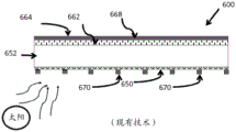
Another field applied on the wafer, which is used in known solar collectors, is called the Back Surface Field (BSF). Conventional cells typically have a back surface field. This field reduces the effective back surface recombination rate and increases the probability of minority carrier collection. A typical way to achieve this is to provide a thin layer of aluminium or an aluminium alloy on the back surface during processing. The application of aluminum has disadvantages. First, it is a separate step in the process, thereby adding complications that would not be present if such an aluminum layer were not required. Second, aluminum is a rather poor reflector of long wavelength light. Thus, when an aluminum back surface layer is present, a relatively high amount of such long wavelength light is not reflected and is lost. It would be beneficial to be able to reflect and thus capture some or all of such long wavelength light. (As a point of clarity, it should be noted that the BSF discussion requires repulsion or reflection of two disparate entities-BSF urges minority carriers away from the back surface.
Therefore, there is a need for a semiconductor wafer that: the semiconductor wafer has a mechanism for establishing an electric field in a direction to urge minority charge carriers (primarily in the thicker portion of the wafer) to the collecting p/n junction. There is also a need for such wafers having excellent electrical properties and acceptably low impurity levels. There is also a need for such wafers doped with dopants that do not have a significant segregation coefficient. There is also a need for wafers of such dopant profiles for p-type semiconductors and also for n-type semiconductors. There is also a need for a method of making such a wafer. There is also a need for solar collectors and solar panels incorporating such wafers.
There is also a need for a wafer for use in a solar cell in which the BSF can be established without the need for processing steps specifically for this purpose, and without the need for an optically weakly reflective aluminum layer at the back surface. There is also a need for a wafer that: such wafers can be configured such that a relatively high amount of reflection of long wavelength light, and thus its capture within the wafer and cell, can be achieved.
Objects of the present invention therefore include a semiconductor wafer having a mechanism for establishing an electric field in a direction to urge minority charge carriers to a collecting p/n junction. Further objects include such wafers having excellent electrical properties and relatively low impurity levels. A further object is such a wafer doped with a dopant that does not have a significant segregation coefficient. Yet another object includes such a dopant-distributed wafer for p-type semiconductors and also for n-type semiconductors. Yet another object is a wafer with a BSF that does not have an aluminum back surface. Still other objects are methods of making any and all such wafers. Yet another object is a solar cell incorporating a wafer with such drift field or BSF or both. Yet another object is a solar cell with higher efficiency for collecting long wavelength light than a cell with an aluminum BSF plane.
Drawings
These objects and others are achieved by the present invention, which is more fully shown in the several figures of the drawings, in which:
FIG. 1A, which schematically shows in cross-section a mold treated with a dopant proximate to a melt of a semiconductor material;
FIG. 1B, which schematically shows in cross-section the treated mold of FIG. 1A in contact with a melt, wherein the upper portion of the melt has some of the treatment material entering the melt;
FIG. 1C, which schematically shows in cross-section the processed mold of FIG. 1B still in contact with the melt, wherein the wafer solidifies on the mold, and wherein a larger portion of the melt than that shown in FIG. 1B has some of the processing material entering a larger portion of the melt;
FIG. 1D, which schematically shows in cross-section the processed mold of FIG. 1C still in contact with the melt, wherein a thicker amount of the wafer solidifies on the mold, and wherein even a larger portion of the melt than that shown in FIG. 1C has some of the processing material entering a larger portion of the melt;
FIG. 2A, which schematically illustrates in cross-section a wafer formed on a mold as illustrated in FIG. 1D, having a gradient profile of doping;
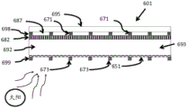
fig. 2B, which schematically shows in cross-section the wafer of fig. 2A after the following processing: doping of n-type material has been added to one side, thereby forming a p/n junction, and a more highly doped region has been formed on the opposite side to the n-type material, which will result in BSF;
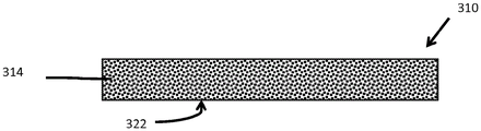
fig. 3, which schematically shows in cross-section a mould of the invention, throughout its volume, said mould being treated with a doping material;
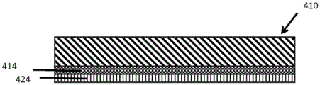
FIG. 4, which schematically illustrates in cross-section a mold of the present invention treated with a dopant material in a pair of layers or coatings on and adjacent to one surface;
FIG. 5 graphically depicts acceptor number (Na/cm) for a representative wafer made in accordance with the present invention3) And a position off the mold side;
FIG. 6A, which schematically shows in cross section a prior art wafer for use in a solar collector having an aluminum alloy back surface electrode;
fig. 6B, which schematically shows in cross-section a wafer of the invention, for use in a solar collector, having a highly doped back surface due to the doping profile, without an aluminum alloy back surface electrode, but with an open grid electrode and a high efficiency optical reflector;
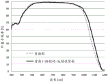
FIG. 7 graphically illustrates the relationship between quantum efficiency versus incident light wavelength for two different configurations, including those illustrated in FIGS. 6A and 6B;
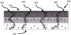
FIG. 8A is a schematic representation of a wafer of the present invention showing segregation of donor compensating dopant atoms at the grain boundaries; and
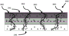
fig. 8B is a schematic representation of the inventive wafer shown in fig. 8A, further illustrating segregation of acceptor anti-compensating dopant atoms at the grain boundaries.
Disclosure of Invention
The wafer is formed on a mold that is provided with a dopant in some manner. For example, the mold can have a coating that includes a dopant. To create a p-type wafer using silicon, the dopant can be boron, which provides an additional electron acceptor. As the mold heats up, the dopant enters the melt (by several possible means), thereby doping the melt region immediately adjacent to the mold so that in this adjacent region the concentration of the dopant (e.g., boron) is relatively high compared to the concentration of the dopant in the bulk of the melt. In a very short time, the semiconductor wafer starts to solidify on the surface of the mold. Dopants such as boron do not diffuse significantly in solid silicon. Thus, after forming the solid wafer, the dopant is no longer able to enter the melt from the mold because the solid silicon on the mold surface acts as a boron dopant diffusion barrier. At this point and thereafter, the concentration of boron dopant in the melt region adjacent the growth surface of the wafer will be less than the concentration present in the melt region where the wafer first began to form. As the wafer continues to grow, new additional regions of the wafer are formed from new growth regions of the melt that have boron dopant concentrations that continue to become less and less over time. This continued dopant reduction in each successive new growth region establishes a concentration gradient or profile of boron dopant where there is a higher concentration at the first solidified wafer adjacent the mold and a lower concentration of boron at the melt side of the last solidified, solidified wafer. The gradient can be tailored by various means. The gradient of doping will produce an electric field that points in a particular direction and the strength of the electric field at any location is related to the degree of gradient at that location and adjacent locations. Such an electric field can have an effect on minority charge carriers in wafers used for solar collectors.
A gradient concentration profile can be useful for creating drift fields within the wafer. Another profile can be useful for creating a back surface field within the wafer. The wafer of the present invention can be used in a solar cell. Due to the drift field, higher efficiency is promoted, which promotes carrier collection within the cell. Higher efficiencies also occur due to the provision of better reflectors on the back surface, which are made possible by the inherent back surface field due to the doping profile, which can eliminate industry standard poor reflectors for aluminum alloy back surface elements.
The characteristic that is related to the local doping concentration in a deterministic way is the local resistivity. There is also a gradient in resistivity and by measuring the resistivity at different locations, the concentration can be determined. An equivalent way of thinking and analyzing the gradient of dopant concentration and the electric field gradient generated thereby is therefore to consider the resistivity profile from one surface of the wafer to the other.
The process invention includes a method of making one such wafer from a melt. The method invention also includes the preparation of a plurality of such wafers from the same melt, including a step to compensate for the accumulation of the predominant dopant in the melt within the melt, which would otherwise be too high to be useful for wafers such as: the wafer is to be fabricated at a target net dopant concentration to achieve a target bulk resistivity for use in a solar cell. Compensation is achieved by periodically providing the melt with compensating dopants of the opposite acceptor/donor type as more and more wafers are formed (e.g., to compensate for the acceptor dopant boron, the donor dopant phosphorus can be used). In some cases, the compensating dopant may segregate disproportionately to the grain boundaries, which may be disadvantageous. In such cases, the present method invention is to add an anti-compensating dopant (in the case of boron (acceptor) and phosphorus (donor) systems, the anti-compensating dopant will be an acceptor such as gallium with a suitably large segregation constant to minimize the electrical effect of the concentration of compensating dopant at the grain boundaries.
Detailed Description
As discussed above, typical semiconductor wafers for use with solar collectors have relatively thick portions in which the majority carriers are of one donor/acceptor type, e.g., typically p-type. Such wafers are formed and subsequently processed so that, in the case of predominantly p-type wafers, one face is doped to have the opposite donor/acceptor type, and hence the majority carriers of n-type. For a typical wafer, the first portion will be substantially the full thickness of 180 microns, while the other type of portion will be only about 0.5 microns thick. The junction between the two parts is called a p/n junction. The following discussion is primarily directed to a novel method for making relatively thick portions, typically p-type portions. The methods discussed below will typically be used to create such wafers. After the method steps discussed herein are performed, a p/n junction and an opposite carrier type portion will be created on one surface. These methods can also be used to create thick, predominantly n-type wafers. In such a wafer of the invention, there will be a gradient profile of doping from one face of the growing wafer to the other. This doping gradient profile will generate an electric field in the finished growth wafer, which can act as a drift field and can also or alternatively act as a Back Surface Field (BSF).
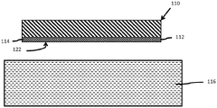
Fig. 1A, 1B, 1C, and 1D show a mold 110 (also sometimes referred to as a substrate) that is provided with dopants in some manner, upon which a wafer 100 (fig. 2A) is to be formed. For example, the mold 110 can have a coating 112 that includes a dopant. To create a p-type wafer using molten silicon, the dopant can be boron (which is a charge carrier acceptor). An alternative embodiment, shown schematically in fig. 3, has a mold 310 with dopants 314 distributed uniformly or in some other pattern throughout its body. Several different embodiments of mold dopant processing are discussed below. The main typical use for the present invention would be with p-type semiconductor wafers and thus with acceptor dopants. Therefore, the discussion will focus primarily on such combinations. However, the invention may also be used with n-type semiconductors and charge carrier donor dopants. (an example of such a system would be a phosphorus doped substrate with boron melt compensation.) yet another more relevant combination is also possible and is discussed below.
The primary dopant, such as boron, can be anywhere on the surface of such a mold 110, or anywhere within the body of such a mold 310. However, it is believed that this provides the greatest advantage if it is present in the region of the mold closest to the melt, such as the coating 112 or a region within the body immediately adjacent the surface, as discussed below. Many different semiconductors can be used as the primary melt component. Silicon is very commonly used and will be used as a representative example in the following discussion. Also, other dopants are possible. In the following discussion, boron will be used as a representative dopant example. However, the generality of the present disclosure is not intended to be limited to silicon as a semiconductor or boron as a dopant. All reasonable alternatives are considered aspects of the invention. For example, for silicon as the semiconductor, examples of dopants include, but are not limited to: boron (B), aluminum (Al), gallium (Ga), and indium (In). For n-type wafers, dopants include, but are not limited to: phosphorus (P), arsenic (As), lead (Sb), and bismuth (Bi).
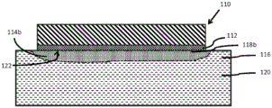
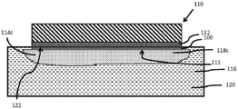
When the mold 110 is heated, such as when it is in contact with a hot semiconductor melt 116, e.g., molten silicon, a dopant 314, such as boron within the mold (fig. 3) or boron 114 of the mold coating 112, enters the melt 116, thereby doping a region 118b of the melt 116 immediately adjacent to the mold 110 such that the concentration of boron 114b adjacent to the mold is relatively high compared to the concentration of boron in a bulk (remaining region) 120 of the melt 116. Embodiments using coating 112 as shown in FIGS. 1A, 1B, 1C, and 1D will be discussed first. As shown in fig. 1C, in a very short time (e.g., milliseconds to several seconds), a semiconductor (e.g., silicon) wafer 100 begins to solidify on the surface 122 of the mold 110.
The mold can be heated in other ways (e.g., it can be preheated before contacting the melt). It is generally advantageous that the mold is cooler than the melt when it is in contact with the liquid silicon, so that heat extraction and thus solidification of the molten silicon is optimally allowed. This solidification process will raise the mold from its starting temperature.
Boron does not diffuse significantly in solid silicon. Thus, as shown in fig. 1C, after forming the solid wafer 100, boron 114 can no longer enter melt 116 from mold/substrate 110 because solid silicon has already been formed on mold surface 122 and acts as a boron diffusion barrier. (this is also typically the case with respect to other dopants and semiconductor wafer systems discussed herein). Typically a thickness of a few microns of solid material is sufficient to prevent further diffusion. This thickness may initially occur at spaced apart locations on the mould surface, but relatively quickly the solidified thickness anywhere on the mould is sufficient to prevent further diffusion. At that point, the concentration 114c of boron in the region 118c of the melt 116 adjacent the growth surface 111 of the wafer 100 will be less than the concentration 114B present in the region 118B where the wafer 100 first begins to form immediately after the mold surface 122 comes into contact with the melt 116, as shown in fig. 1B, because the boron 114c atoms diffuse and move away from the mold 110 and the growing wafer 100 and away from the region 118c adjacent the growth surface 100 of the mold 110 and the wafer 100 into the melt 116 by convection.
As the wafer 100 continues to grow (i.e., thicken) during the next few seconds of the timescale, new additional regions forming the wafer 100 are formed at the surface 111 from new growth regions 118c, 118d of the melt adjacent to the growth surface 111, the new growth regions 118d having a boron concentration 114d that continuously becomes less and less over time. For each successive amount of growing wafer, the newly grown region is always so slightly progressively further away from the mold, the initial source of dopant. The dopant has rapidly diffused into the bulk 120 of melt 116 away from mold 110.
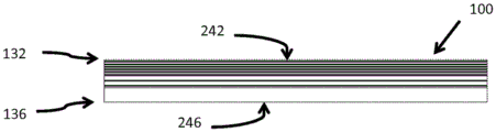
Fig. 2A shows a grown silicon wafer 100. The continued reduction of dopant in each successive new growth region establishes a gradient of dopant boron in the grown wafer 100, as shown in fig. 2A, with a higher concentration of boron being present at the portion of the wafer adjacent to the mold 110 and its surface 122, as the wafer completes its formation, with the surface 132 first solidifying from the region of the melt 116 when the region of the melt 116 has a relatively higher concentration of boron. There is a lower concentration of boron at the surface 136 of the solidified wafer 100, at times and locations where the melt has a relatively lower concentration of boron, the surface 136 eventually solidifies from a region of the melt 116 (relatively far from the mold surface 122, having a boron content at that location).
The foregoing discussion is arranged in terms of successive regions of the growing wafer 100 and successive new growing regions of the melt as if the growing regions were discrete, layer-by-layer, such as multiple sheets of paper. In practice, the growth of the wafer is continuous, atom-by-atom, and the diffusion of the dopant into the melt is also continuous, atom-by-atom. The amount of dopant incorporated into the growing wafer depends on the relative diffusion rates of the dopant into the melt, away from and out of successive newly grown regions of the melt, and the growth rate of the semiconductor wafer. These two rates are influenced by the diffusion tendency of the dopant in the melt, the temperature, the crystal growth rate, etc. Thus, the concentration of boron in the wafer varies smoothly from the surface 132 formed closest to the mold to the surface 136 formed deeper within the melt, further away from the mold. (FIG. 2A shows three different regions of the formed wafer, with three different discrete dopant concentrations, the concentrations indicated by the closeness of the horizontal hatching, the tighter hatching indicating a greater dopant concentration this is not meant to actually represent the formed wafer, but is merely a limitation of the figure, which must show the physical situation from the surface 132 adjacent to the mold formation to the surface 136 further away from the mold formation in black and white, which might be better shown in the continuation of the gray scale).
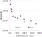
Fig. 5 shows the p-type doping concentrations for two different wafers (designated wafer 1 and wafer 2), each showing: approximately 1 x 10 at the first formed wafer portion immediately adjacent the mold19 Na/cm3In a smooth curve having a roughly exponential decay shape, wherein N is in a range of positions from about 25 to about 150 microns from the first-formed wafer portion immediately adjacent the molda/cm3At a concentration of about 1X 10¹⁷And 1.5X 10¹⁷In the meantime. Up to 1X 10²⁰ Na/cm3N of (A)aIs considered possible, and is also believed to be as low as 1 x 10 at the location of the last formed wafer furthest from the mold15 Na/cm3Is possible. Unit NaRepresenting the number of acceptors, as in electron acceptors. For an N-type dopant, the corresponding unit would be NdWhich represents the number of donors, as in electron donors. (in some cases below and in the claims, as the case may be, depending on whether an electron donor or acceptor is intended, the expression N is expressedxFor representing NaOr Nd). As can be seen, the transition from the relatively high concentration to the relatively low concentration is smooth and continuous.
Semiconductor wafers not known to have such a doping gradient have been previously fabricated except in the very limited type mentioned above using the Stichting method. As discussed above, this approach creates semiconductors with very poor electrical properties.
Reviewing the hypothetical example outlined above for the impurity and Sticting method, there is a doping difference factor of 10, and thus the same impurity difference, in the wafer, and 5 x 10¹¹Atom/cm3Resulting in a minority carrier lifetime of about 7 microseconds, resulting in an efficiency of 16.4%, wafers prepared according to the invention will have significantly better properties. Such a wafer would have 5 x 10 in the wafer10Atom/cm3Resulting in a minority carrier lifetime of about 70 microseconds, resulting in an efficiency of 18.4%. This example is hypothetical, and any other factors would go into any practical physical situation, but the comparison is appropriate.
In the dopant-distributed wafer of the present invention, if formed from a melt doped with a p-type material, the wafer is formed first, and then the opposite type (in this case, n-type) of material will be created on one surface, thereby creating a p/n junction. Fig. 2B schematically illustrates the relationship between the p/n junction and the doping profile of the present invention. For a melt-formed p-type wafer having a doping profile as discussed above, the p-side (more positively doped side) of the wafer 100 will be the side 242 with the higher concentration of p-type dopant boron, formed closer to the mold surface 122. The n-side (the less positively doped side, or the more negative side) of the wafer will form on the side 246 having the initially lower concentration of p-type dopant boron, which is formed further from the mold surface 122. Forming the n-type (or oppositely doped) portion 250 can be accomplished by any conventional or yet to be developed method. Typically such portions are only about 0.5 microns thick in depth. In a typical application, boron p-type doping provides about 1 × 10¹⁶/cm3N of (A)a. n-type doping provides about 1 x 10¹⁹/cm3N of (A)d. Thus, at side 246, n-type doping dominates. A p/n junction 252 is located between the n-type portion 250 and the side 246 having the initially lower p-type dopant concentration. The sun-facing side of the wafer will have an n-type portion 250 facing the sun. Also shown on the opposite side to where the sun will be is a back surface field part 254 (discussed in more detail below) adjacent to the side 242 having the initially higher p-type dopant concentration.
As discussed above, such a dopant gradient is beneficial because it establishes an electric field directed towards the collecting p/n junction with respect to the minority carriers. The electric field causes the generated minority charge carriers to preferentially move towards the p/n junction. This directional preference increases the collection efficiency of the solar cell. It is believed that this effect cannot be achieved by any conventional melt doping method. (in p-type semiconductors, minority carriers are electrons).
It should be noted that considering the dopant concentration at different locations within the wafer body is only one way to describe its structure and properties. Another way is to consider the material resistivity at the same different locations throughout its body. The following is also true: due to the different net doping concentrations, there will be corresponding and correlated differences in the resistivity of the wafer at different locations throughout the body. Thus, there is also a gradient in the resistivity of the bulk, which is generally opposite to the net doping gradient. This means, therefore, that the resistivity is higher in the regions of lower dopant concentration, while the resistivity is lower in the regions of higher dopant concentration. It is also noted that although these gradients of concentration and resistivity are generated by the phenomena of melt solidification and segregation described above, it is relatively difficult to measure the material concentration at different locations within the wafer. However, it is easier to measure the resistivity at such locations through the body. (this can be done by measuring the resistivity of the body, removing a layer of material, and measuring the resistivity of the remaining body, whereby it is possible to determine the resistivity of the removed part from the difference). From this determined resistivity it is also possible to determine the material concentration, i.e. the doping concentration, of the layer that has been removed. One layer after the other, the resistivity profile, and thus also the doping concentration profile, through the entire body can be measured and thus determined.
The relationship between resistivity and dopant or carrier concentration is deterministic and non-linear. Table 1 below shows the correlation of the resistivity (ohm-cm) to the acceptor carrier concentration (atoms) on the one hand/ c3) A representative set of values that are related and also related to donor carrier concentration:

table 1-relationship between resistivity and carrier concentration.
The relationship can also be characterized graphically, such as in a log-log graph. Such a graph is shown on www.solecon.com/pdf/converting _ responsiveness _ to _ carrier _ concentration _ graph _ sig. This is the work shown by the website of Solecon Laboratories of Trademark Dr., Reno, NV. The graphs shown therein are hereby incorporated by reference in their entirety. Vertical scale indicates carrier concentration/cm3Wherein the horizontal scale represents resistivity (ohm-cm). The relationship between carrier concentration and resistivity generally shows that higher concentrations correlate with lower resistivity, and vice versa. On a log-log scale, the slope is usually negative. The profiles for n-type and p-type doping of the same semiconductor, e.g. germanium, are generally identical and spaced apart, with the profile for p-type being shifted towards the right, typically so that for the same carrier concentration in the n-type semiconductor, there will be a higher resistivity in the p-type semiconductor. The relationship between carrier concentration and resistivity of silicon semiconductors is generally the same as described for germanium semiconductors. Values were determined using extended resistance analysis (SRA). The authors explain that, in order to calculate The value of The carrier concentration of Silicon, they used mobility values obtained from The National Bureau of Standards specific Publication 400-64, The relative bed best resistance and dose sensitivity for phosphor and Boron-subject Silicon (5 months 1981), Table 10, page 34 and Table 14, page 40, by Thurber, Mattis, Liu and Filiben. To calculate the germanium carrier concentration values, they used carrier mobility values obtained from Bell System Technical Journal (3.1961) of D.B Cuttiss, page 509.
The above process works very well without modification for creating one or a small number of wafers from a single melt without adjusting the melt composition.
One challenge presented by this process is that it will result in an increase in the concentration of dopants (such as boron) in the melt over time as more and more wafers are produced without modification. That is because less than all of the boron that was moved from the mold during the time that a single wafer was produced will be incorporated into the wafer being formed during that time interval. This concentration build-up in the melt limits the number of wafers that can be grown before the melt becomes overly rich in dopant (e.g., boron) for the baseline doping level. Precisely whatever the dopant provides, the electron donor or acceptor, the melt has become overly rich. Finally, an equilibrium is reached where the amount of boron removed from the melt at the formation of each wafer is equal to the amount of boron added to the melt from the mold at each wafer growth cycle. The boron concentration at which this equilibrium is reached is generally too high to produce good quality conventional solar cell wafers from a dopant rich melt.
To compensate for this accumulation of boron in the melt, a quantity (specified below) of a different material (referred to herein as a compensating dopant), such as the compensating dopant phosphorus in the case of a boron primary dopant, can be added directly to the melt. (as explained below, in some cases there is a reason for requiring yet another compensating dopant (for a different reason), and thus in some cases this compensating dopant to be described may be referred to as the first compensating dopant).
Boron is a member of group III of the periodic table and has a tendency to accept or accept one electron. Thus, boron is an electron acceptor. Phosphorus is a member of group V of the periodic table of the elements and, therefore, has excess electrons that can be donated to the melt. Thus, phosphorus is an electron donor. Thus, the phosphorus compensates for the excess electron acceptor boron, since the phosphorus provides electrons that the excess boron tends to accept, thus compensating for the excess boron acceptor. A single phosphorus atom donates a single electron, while a single boron atom accepts a single electron.
Phosphorus added in an appropriate amount will compensate for the excess boron and maintain the wafer formation process at the desired boron dopant level indefinitely. The amount of phosphorus (compensating, donor dopant) to be compensated (as measured by atomic number) is approximately equal to the amount of boron (excess, primary, accepting dopant) in the melt (as measured by atomic number) multiplied by the segregation coefficient k of boron and divided by the segregation coefficient of phosphorus (specifically, k = 0.8 for boron and k = 0.3 for phosphorus).
In other words, the melt doping (concentration of acceptors or donors, as the case may be, depending on the p-type or n-type semiconductor) should ideally be maintained at or near the following conditions: under this condition, a wafer grown on a mold without the dopant material contained in any part of the mold or mold coating will have a high resistivity, such as typically greater than 1 ohm-cm for n-type and greater than 2 ohm-cm for p-type. To achieve this, the amount of compensation doping material of the opposite type to the main type present in the mould or coating should preferably be present in the melt at a concentration described by the following relationship:
Ccdis approximately equal to Cmd *(kmd / kcd)
Wherein:
Cmdis the melt concentration of the mold primary dopant (e.g., boron);
Ccdis the melt concentration of the compensating dopant (phosphorus for the above example of boron primary dopant);
kmdis the effective segregation coefficient of the main dopant of the mold; and
kcdis the effective segregation coefficient of the compensating dopant.
The resulting wafer will have a measurable boron concentration gradient (see FIG. 5), for example, from about 1X 10¹⁹ Na / cm3To about 1X 10¹⁷ Na / cm3. One aspect of the invention disclosed herein is an article of manufacture that has a measurable concentration of a primary dopant (such as boron) as measured from one surface to an opposite surfaceGraded wafers. In fact, the reasonable minimum difference between the doping on the melt side and the doping on the substrate side is a factor of three. This results in a 0.1% increase in efficiency compared to a flat doping profile containing the same number of acceptors. The magnitude of the gain depends on many factors such as cell architecture, minority carrier lifetime of the wafer, surface passivation, etc. The above example is achieved with a PERC architecture (0.1% gain, 1/3 pre-post doping difference. in the case of an aluminum BSF architecture, the gain may be different. As mentioned above, it is difficult to directly measure the dopant (such as boron) concentration within the bulk of the wafer.
The compensating dopant should be added periodically or continuously to match the rate of addition of dopant from the die.
Thus, another aspect of the invention disclosed herein is a method of fabricating a wafer, and a more specific aspect of the method invention disclosed herein is a method of fabricating a wafer having a measurable dopant (such as boron) concentration or resistivity gradient as described above, and the present specific method invention is the following method: over time, a plurality of such wafers are produced from the melt while maintaining relatively similar doping and resistivity profiles, even as more and more wafers are produced and more of the primary dopant enters the melt.
Turning now to a discussion of the location of the dopant source to be incorporated into the wafer, a typical location is shown in fig. 1A, such as a coating on the shaping surface 122 of the mold 110, or somewhere within the body of the mold 110, as shown in fig. 3 and 4, in a location where the dopant is able to move through the body of the mold to exit the mold and dope the melt 116 when the mold is heated. Thus, as shown at 114 in fig. 1A, the dopant may be in the outermost layer 112 of the coating (such as the release layer) on the mold 110. Alternatively, as shown in fig. 3, it may be located within the body of the mold 310, evenly distributed or in a more concentrated area, such as more concentrated closer to the forming surface 322. Alternatively, as shown in fig. 4, it may be located in a buried layer 414 of the coating on the mold, with another layer 424, such as a release layer, at the surface.
More specifically, the mold 310 itself can contain volatile boron-containing compounds such as: boron oxide, boron nitride, boron, boric acid, and borosilicate glass. Alternatively or additionally, the mold coating 112 in intimate contact with the melt can contain volatile boron compounds and boron compounds that are soluble in silicon (in the case of forming silicon wafers, otherwise soluble in the semiconductor being formed), including: boron oxide, boron nitride, boron, boric acid, borosilicate glass, boron carbide, silicon boride. Still further alternatively or additionally, the die coating area not in intimate contact with the melt can contain a volatile boron compound comprising: boron oxide, boron nitride, boron, boric acid, borosilicate glass.
Another issue to consider with respect to the location of the dopant is the manner by which the dopant is transferred or migrated from the mold to the molten material. It is believed that there are three different main possibilities. One would be to dissolve the dopant into the molten silicon and then diffuse further into the melt. This form of dissolution and diffusion is believed to confer a number of benefits. The second would be diffusion from the mold into the liquid of the melt. The third and presently least preferred is evaporation from the mold into the melt.
Turning to each of these in turn, the most preferred would be from the mold such as at B4C (boron carbide) or B4Where the dopant in the form of Si (silicon boride) will dissolve from the mould (such as from the coating) into the melt. Within the melt, the dopant will decompose into its constituents, and the dopant, such as boron, will diffuse further into the bulk of the molten material. To the extent that they have not yet saturated them in the melt, e.g. very muchThis may be the case, as other components such as C or Si will also diffuse. The advantage resulting from this approach is that each wafer produced on the same mold receives the same amount of dopant, unlike other approaches, such as the third mentioned below, where more dopant is released for earlier produced wafers.
The second way in which the dopant diffuses from the mould directly into the liquid, will diffuse from the coating or from the mould itself into the melt is considered to be the least likely, as most, if not all, of the material will enter the melt by some mode other than diffusion alone, such as by dissolution or evaporation. In any case, diffusion will occur to some extent for all modes in which the dopant is actually in contact with the melt.
The third mode, direct evaporation, is not preferred. For example, B may be2O3(boron oxide) or BN (boron nitride) is heated to the following extent: it evaporates directly from its location on the mold (e.g., in the coating) or its location in the mold to pass directly into the molten semiconducting material as a gas. This is not preferred as it would be expected that it would be difficult to control the extent to which the dopant is released into the melt. The entire source of dopant heats up at one time and will release boron by evaporation, not just the portion of the dopant source that is in contact with the melt. Thus, more dopant will be released the first time the mold is heated, e.g., small particles may disappear after only one thermal cycle. Or the process is limited by the diffusion of dopant particles to the surface of the mold.
Some examples are illustrative as to both the location and manner of the dopant. For doping from a mold coating (such as a release coating) in direct contact with the melt (such as shown at layer 424 in FIG. 4 or at layer 112 in FIG. 1B), a suitable dopant source would be Si when minimal vapor transmission is desired3N4Or SiO2Of the coating material, and B4C or SiB4The dopant of (1). For a material never in direct contact with the melt (such as shown in fig. 4 at buried layer 414Of (d) and a suitable dopant source would be Si3N4Or SiC, and BsO3Or a dopant of BN. For doping from a mold rather than a coating (such as shown at 314 in FIG. 3), a suitable mold material would be SiC, and B2O3Or a dopant of BN.
The basic method described above will also work for: any other P-type primary dopant than boron (such As aluminum (Al), gallium (Ga), indium (In)), and any suitable n-type dopant is used to compensate the melt (phosphorus (P)), arsenic (As), antimony (Sb), bismuth (Bi)), respectively. However, the pair of B and P is considered to be extremely advantageous for use in growing silicon wafers because of their highest numerical segregation coefficient in silicon among all available dopants. (during solidification, elements with relatively higher segregation coefficients segregate relatively less than other elements, and as such, during solidification, those with the highest segregation coefficients segregate least.) thus, at solidification, the dopant B and the compensating dopant P will be distributed relatively uniformly within the crystal, compared to what would arise if elements with numerically smaller segregation coefficients (with greater tendency to segregate) were used. A similar but related process can also be used to prepare predominantly n-type doped wafers. In that case, the primary dopant provided by the mold or coating thereon will be an n-type dopant (such As P, As, Sb, Bi) and the melt compensating dopant will be a P-type dopant (such As B, Al, Ga, In).
Table a below shows representative main and counter dopants for p-type and n-type semiconductors and their respective segregation coefficients:

table a-dopants and equilibrium segregation constants.
This method of doping semiconductor materials can be applied to any semiconductor that can be grown from the melt, including silicon (Si), germanium (Ge), gallium arsenide (GaAs), and the like. Growing a semiconductor wafer/body from a semiconductor material other than silicon would require the use of different dopants (e.g., silicon as the primary dopant for a GaAs wafer) and different compensating dopant materials.
Table B below shows compounds of doping elements that can be used as sources. The x label means that a compound is present, for example, boron carbide, boron oxide, and the like. (in contrast, for P, As, Sb, Bi, no silicide is present). Pure elements may also be used, and any compound of Si, C, O, N may be doped with any of the elements and then used as a source for the dopant. Some of the listed compounds are present but are impractical due to low stability, reactivity with moisture, toxicity, etc.:

table B-compounds of doping elements.
The invention disclosed herein imparts numerous benefits. One benefit is a beneficial electric field that improves minority carrier collection and, therefore, improves the efficiency of the solar cell. Another benefit is higher efficiency at lower resistivity, which means that higher fill factors are possible. Possibly also in synergy with PERC-like processes (lower resistivity is beneficial for PERC-like cell architectures). (PERC stands for passivated emitter back contact).
Yet another benefit is related to the fact that the gradient of the dopant (or its associated, resistivity) is able to automatically generate a passivating field. (this is evidenced by the very high doping concentration in the portion of the wafer closest to the mold formation, as shown on the left hand side of the curve shown in fig. 5). The passivating field will reduce recombination at the back surface. The benefit is that the conventional aluminum BSF (back surface field) that would conventionally be applied during cell processing is not necessary and can be eliminated. This will then reduce the number of steps to form a typical cell.
Another advantage results therefrom. If the Al BSF is not required to be present, an open grid contact can be used on the back side of the wafer, allowing long wavelength light to pass through the cell and be efficiently reflected at the reflector plate on the back side of the module, and then pass back through the cell again. This is discussed in more detail below.
The so-called Back Surface Field (BSF) can also be provided by a gradient of doping (and its associated resistivity) through the thickness of the wafer. Fig. 6A schematically illustrates in cross-section a known solar cell 600 incorporating a BSF. The BSF is created by a region 662 of particularly high concentration of dopants at the back side of the solar cell (the surface facing away from the sun), which creates a strong electric field within the semiconductor material at the back side of the cell. This electric field repels minority carriers near the back of the cell and prevents the majority from reaching the characteristic back surface 664 of the semiconductor material. This is important because if they were to reach the back surface 664, it is likely that they will recombine at that surface and thus no longer be available to create current in an external circuit.
Both the drift field and the back surface field depend on the spatial variation of the doping density through the wafer thickness, with higher doping density towards the cell back side and lower doping density towards the cell front side. However, they differ in several important respects. First, the drift field is most effective when it extends through the wafer thickness, as such it will keep the minority carriers gently pushed towards the collection point (rather than letting it only undergo diffusion). Instead, the BSF is limited to the back side portion of the cell wafer. For example, in a 180-200 micron thick cell wafer, the BSF region of the cell wafer may be 1-10 microns thick, with a typical thickness of about 5 microns. Further, the doping level in the BSF is very high to create a high electric field, which then effectively repels minority carriers towards the front. In fact, the doping level is so high that it can negatively affect the minority carrier diffusion length (or lifetime) in the rear part of the cell. The net effect on device performance is still very positive because the reduction in diffusion length is localized to the cell's characteristic back side only, and because the BSF itself minimizes the number of carriers entering this region. Conversely, a lower doping level in the drift field has a relatively small negative effect on the minority carrier diffusion length. Such a BSF battery is shown in fig. 6A.
The most common way to create a BSF is to screen print an aluminum paste onto the back side of the wafer and burn it in a belt furnace. This results in a region 662 of silicon with very high doping density of aluminum (p-type dopant). Further, behind this, there is a layer 668 of an aluminum-silicon alloy (many of which are eutectic compositions). The aluminum alloy region serves as the back contact/conductor of the cell. Unfortunately, aluminum-silicon alloys are not particularly good optical reflectors for the operation of such conventional BSF cells, having a reflection coefficient of about 60%. Thus, 40% of the infrared light that is not absorbed when it first passes through the battery body 652 is absorbed by the back contact and is no longer available to travel back through the battery body 652 in a second pass. This significantly limits the current generated by the battery and limits the voltage to a small amount. The sun-facing surface of the cell may be provided with a textured surface 650 and electrical contact fingers 670.
As shown in fig. 6B, the present native doping can provide a region 682 with a doping profile that functions as a BSF without the above-mentioned disadvantages. In certain embodiments, this region 682 (for the back surface) that is particularly highly doped can be created along with a broader region 692 of distributed drift field doped through the thickness of the cell wafer. (As shown in FIG. 6B, the region 692 has no graphical representation of the doping profile to simplify the figure. however, it should be understood that there may be a flat or less flat doping profile similar to that shown in FIGS. 2A and 2B as discussed above.) in other embodiments, the flux (flux) of dopant from the mold or mold coating can be designed to be more narrowly confined to the back side of the cell wafer. This can then be used to create a significantly doped BSF region 682, and also create a drift field region 692 that is only very lightly doped, so that its gradient will be very gradual or less steep despite the drift field that would be present. Alternatively, both effects can be achieved with the same doping or with different doping patterns.
There are several methods for creating the native doping that functions as a BSF. A typical BSF will have a value of about 1 × 10¹⁸/cm3A recipient. To achieve this, a large amount of acceptor dopant, such as boron, will be provided within the mold. To enhance the back-side doping compared to the front-side doping, the semiconductor crystal can be grown relatively slowly after the initial nucleation, which will provide more time for the acceptors already in the melt to diffuse deeper into the melt, away from the solidified crystal, allowing a much lower acceptor (boron) concentration in the bulk of the crystal compared to the initial layer grown immediately adjacent to the mold. The strength of the BSF is proportional to the ratio of doping at the back side to doping in the bulk of the wafer. Additionally or alternatively, nucleation can be enhanced by providing a higher vacuum (or pressure differential) during an earlier portion of solidification, as discussed below. This will result in the crystal solidification and growth starting earlier, while the dopant concentration will be formed in the vicinity of the mould, in the part of the melt from which the body will solidify. Techniques for varying the vacuum (or pressure differential state) over time or in different locations are described in the above-referenced Sachs et al patent No. 8,293,009. The following wafers have been prepared: the wafer has a1 x 10 thickness at the surface of the wafer formed adjacent the mold face18/cm3Carrier concentration of the acceptor.
The above mentions adjusting the vacuum pressure or pressure differential state during solidification. This is referred to the method disclosed in the' 8,293,009 patent. It is beneficial that the mold described therein is porous (as discussed below). A pressure differential is provided between the mold surface in contact with the surface of the molten material and the back surface of the mold such that, upon contact, the molten material is drawn toward the mold face. The porosity of the mold is such that molten material is not drawn into the pores. This is achieved by: the pores are small enough that surface tension and other phenomena prevent the molten material from entering the pores before the material solidifies. They are also sufficiently large to enable a pressure differential to be established despite their small individual dimensions. The pressure differential can be established by: providing a vacuum, or by providing a surface of the molten material at a pressure above atmospheric pressure, with the opposing surface of the mold at a lesser pressure, such that the pressure differential provides a force that forces the molten material and then the solidified body toward the mold face. By providing such a pressure differential, the contact force between the molten material and the mold face is increased compared to the case without the pressure differential, which provides for more rapid solidification. Enhanced pressure differentials may also be provided at various locations across the mold face, as opposed to other non-enhanced locations, by various means, such as thermal inserts or voids at specific locations in the mold face. By porous it is meant a body that is filled with very small pores and channels so that there is a continuous path for the gas to flow from one surface of the mould to the other. The pores are very small. It is typically on the order of microns, such as 10 microns in diameter, possibly up to 30 or 40 microns in diameter. There are many that cover the surface of the mold and pass through the bulk of its body. The path is curved, such as in natural sponges. As defined herein, porous does not include macroscopically simple voids that pass from one surface to another, such as holes drilled through a die body.
Fig. 6B shows a cell wafer 601 with BSF regions 682 and with a back electrode 698 in the form of fingers 671 similar to fingers 673 of electrode 699 with the front side facing the sun, which also shows fingers. An optical (typically white) reflector 695 (which may be specular or diffuse) is behind the back electrode 698 (relative to the sun). The reflector may be a back plate used during packaging of the module. There may be a physical space 687 between the back surface of the cell wafer and the reflector, or there may be no space. In this manner, photons that are not absorbed as they pass through the main body 693 of silicon for the first time will exit the cell wafer, be reflected by the optical reflector 695 and re-enter the cell wafer from the back surface for a second pass through the main body 693 of silicon and additional opportunity to be absorbed. The optical reflectivity of the majority of the back contact is in that case dictated by the reflectivity of the material placed behind the cell wafer, which may be greater than 90%, and in many cases greater than 95%. The sun-facing surface of the cell wafer may be provided with a textured surface 651 similar to the prior art embodiment shown in fig. 6A.
Fig. 7 shows diagrammatically the Quantum Efficiency (QE) measurements for two types of cells. The optical response for the structure shown in fig. 6A is shown in dashed lines and is generally inside the other curve. The optical response for the structure of the present invention with the native BSF and the reflective backplane shown in fig. 6B is shown in solid lines and generally outside of the other curve. Thus, as can be seen, the photoresponse of the cell is higher for the inventive structure shown in fig. 6B. As expected, the increased QE is in the infrared region of the spectral wavelengths on the graph from 900nm to 1200nm, since it is at these longer wavelengths that it is able to penetrate to the back of the cell. The result is a more efficient cell.
The basic cell structure and some form of BSF of the wafer, such as provided by fusion of aluminum during the contact firing step, are known in the art, being backed by open areas, grid-like electrodes and reflectors. One example is a PASHA battery structure. It is also known to provide the BSF by a separate doping step to provide a heavier doping near the back surface of the cell. Creating such a structure requires this separate doping step. The present invention is believed to create such doped BSFs without a separate step for creating such doped BSFs, i.e., by creating BSFs along with drift fields during the growth phase of the wafer, as explained above. Thus, another invention herein relates to a novel and non-obvious method of fabricating such a structure, wherein the doping required to create the BSF is created during the wafer growth process according to the method discussed above.
It has been determined that in any particular system, such as using silicon as the semiconductor, boron as the primary dopant, and phosphorus as the counter dopant, undesirable conditions may arise. Recall that: as many strings of wafers are produced from the same container and melt, compensating dopants are added to the bulk of the melt over time to keep the resistivity of each newly produced wafer in the series of wafers produced from the same melt the same. This must be done despite the fact that there is an increased accumulation of the primary dopant (e.g., boron) in the melt over time.
An undesirable phenomenon is that a compensating dopant having a lower segregation coefficient than the main dopant segregates more strongly to the grain boundaries. See, for example, fig. 8A, which schematically illustrates a Si crystal 800 and a low segregation coefficient compensating dopant D that accumulates at the grain boundaries 860. This is generally undesirable because the higher concentration of compensating dopant D near the grain boundaries 860 results in a higher concentration of the carrier type D (in the case of P, these are donors and therefore the letter D is used to denote them) near the grain boundaries that is required by the compensating dopant. As such, an electric field directed at the grain boundaries will be established within the grains, and thus, minority carriers will be drawn to the boundaries. Such a situation is undesirable because that is not where it is desired to direct these carriers. They are directed away from the surface 242 of the wafer having a higher concentration of acceptor dopant a toward the p/n junction (not yet formed and therefore not shown in fig. 8A) that will be formed adjacent to the surface 246, which surface 246 has a lower concentration of acceptor dopant a.
It has been determined that this undesirable effect can be overcome by the counter-intuitive step of providing a second compensating dopant, referred to herein as a counter compensating dopant, such as aluminum (Al) counter compensating dopant in the case of the Si/B/Ph system. Aluminum is the same type of carrier donor/acceptor as the primary dopant. Thus, aluminum is an acceptor, as is boron. Most advantageously, the segregation coefficient of the counter compensating dopant is numerically smaller than the segregation coefficient of the first compensating dopant and numerically as close as possible to the coefficient value of the first compensating dopant. With a numerically smaller segregation coefficient, the counter compensating dopant migrates even more strongly to the grain boundaries than the compensating dopant. Thus, at these boundaries, it is the acceptor/donor role that offsets the excess donor/acceptor present due to the relatively high concentration of compensating dopant.
In the case where the segregation coefficient of the primary dopant is lower in value than the segregation coefficient of the first compensating dopant, it is not necessary to use a second, counter compensating dopant (and thus the compensating dopant is simply the compensating dopant rather than the first compensating dopant). A very useful combination for silicon semiconductors uses boron as the primary dopant, phosphorus as the counter dopant, and Ga (gallium) as the second counter-dopant. B has the largest segregation coefficient (smallest segregation), 0.8, followed by 0.3 of P and 0.008 of Ga.
Table C shows different combinations of primary (substrate) dopants, compensating dopants, and second counter compensating dopants for both P-type semiconductor crystals, such as silicon, and N-type semiconductors as shown in table a, but with additional information regarding the counter compensating dopants. The segregation coefficient for each element is also provided when referring to the element for the first time:

table C-combination of primary, compensating and counter compensating dopants for P-type and N-type semiconductors.
The compounds listed in table C above can be used to provide the counter compensating dopant as well as the primary and compensating dopants. In the case where both an n-type dopant and a p-type dopant are added to the melt, a second, counter-compensating dopant can be added using the compound semiconductor. For example, in the case of a boron primary dopant, InP (indium phosphide) can be used. Phosphorus will provide the compensation doping and indium will provide the counter compensation in the same way as Ga in the table above. But P and In will be provided as complexing agents rather than as separate additives.
Examples of the invention
Wafers have been grown and solar cells have been prepared. Solar cells show high efficiency at very low resistivity. For example, solar cells fabricated on wafers using this method have an average bulk resistivity of only 0.3 ohm-cm, with an efficiency 2% higher than control wafers having a resistivity of 2.2 ohm-cm. The doping profile schematically shown in fig. 5 is measured by: the silicon is selectively removed layer by layer and the resistivity of the remaining wafers is measured. Generally, there is a lower resistivity in the regions with higher dopant concentration, and vice versa. Furthermore, wafers exhibiting a resistivity profile, having a lower resistivity at one surface (typically the back surface not facing the sun, where there is a higher dopant concentration in a p-type wafer) and a higher resistivity at the other surface (in that case, it would be the surface facing the sun), are considered to be the present invention, as are solar cells comprising such wafers and methods of making such wafers.
An average net acceptor concentration of about 5X 10¹⁵ /cm3With about 10 times more doping at the back surface (formed on the side facing the mold). The cell has an aluminum back surface field instead of the native BSF, also as discussed above. Boron dopant of about 1 x 10¹⁸Atom/cm3. The impurity content is minimal and in any case less than 10 times the amount present at equilibrium segregation. The following ranges of compensating dopants exist: from none (at the very beginning of the run) to about 1X 10 at the end of the run18Atom/cm3(about 2,000 wafers were prepared therein.
The invention disclosed herein solves a number of problems. The present invention allows for the low cost establishment of a dopant gradient from one surface of the formed wafer to another. Heretofore, it has been known that methods of establishing dopant gradients in silicon wafers result in low quality silicon (such as gallium-doped RGS (ribbon growth on substrate) or are very expensive (epitaxially grown silicon).
It should be noted that many/any of the foregoing techniques for providing a profile of doping levels to a wafer can be used with any other technique. For example, any manner of providing dopant to the mold (e.g., in a coating, in the body of the mold, or near the mold surface) can be used with any method of compensating for excess dopant in the melt over time, and any method of compensating for excessive segregation of dopant to grain boundaries back can also be used with any other method of providing a doping profile. Providing dopants to some extent and in locations to create a BSF can be used with any technique for dopant compensation and also for counteracting the accumulation of compensating dopants at grain boundaries. The techniques for forming any curve or shape of dopant profile can be used with compensation and anti-compensation techniques and also with methods of forming BSFs.
The present disclosure describes and discloses more than one invention. The invention is set forth in the claims of this document and related documents not only as filed, but also as proposed during the prosecution of any patent application based on this disclosure. The inventors intend to claim all of the various inventions as they are subsequently determined to be as maximum as the prior art allows. The features described herein are not required for every invention disclosed herein. Accordingly, the inventors intend that features described herein should not be incorporated into any particular claim based on the disclosure, except for the features claimed in any such claim.
For example, the invention of the drift field is not essential to the invention of the BSF, and vice versa. A gentle drift field can be established and it does not have an extremely highly doped BSF. The BSF can be provided with a relatively highly doped region and the rest of the wafer can be relatively uniform, with substantially no drift field, or only a slight degree of drift field. For single wafer formation, or even for a cluster of wafers, it is not necessary to provide a compensating dopant in the melt, as long as the concentration of the predominant dopant in the melt does not become too great to form a good quality wafer. Other methods of dopant compensation can be used. Similarly, there is no need to use an anti-compensation method to prevent excessive accumulation of compensating dopants at grain boundaries, which is disclosed herein to provide counter dopants with even smaller segregation coefficients. For some applications, such accumulation can be tolerated, or other methods of counteracting the accumulation can be used.
Some combination of hardware or set of steps is referred to herein as an invention. However, it is not an admission that any such combination or group must be a distinct invention with patentability, particularly as contemplated by laws and regulations regarding the number of inventions or the uniqueness of the inventions as they will be reviewed in one patent application. It is intended to be a brief way of illustrating embodiments of the invention.
The summary is filed herewith. It is emphasized that this abstract is provided to comply with the rules requiring an abstract that will allow examiners and other searchers to quickly ascertain the subject matter of the technical disclosure. The abstract is submitted with the understanding that: it is submitted with the understanding that it will not be used to interpret or limit the scope or meaning of the claims, as intended by the rules of the patent office.
The above discussion should be understood as illustrative, and should not be considered restrictive in any sense. While the present invention has been particularly shown and described with reference to the preferred embodiments thereof, it will be understood by those skilled in the art that various changes in form and details may be made therein without departing from the spirit and scope of the invention as defined by the appended claims.
The corresponding structures, materials, acts, and equivalents of all means or step plus function elements in the claims below are intended to include any structure, material, or act for performing the function in combination with other claimed elements as specifically claimed.
Aspects of the invention
The following aspects of the invention are intended to be described herein and this section is to ensure that they are mentioned. They are named as facets and although they look similar to the claims they are not. However, at some point in the future, the applicant reserves the right to claim any and all of these aspects in this and any related applications.
A1. A method for fabricating a semiconductor wafer for use as a solar collector, the method comprising the steps of:
a. providing a molten semiconducting material having a surface;
b. providing a mold comprising a shaped surface, the mold further comprising a primary dopant associated with the semiconductor material;
c. contacting the shaping surface with the molten material such that dopants migrate from the mold into the molten semiconducting material; and
d. conditions are maintained such that a body of semiconductor material in wafer form solidifies on the shaping surface with a first surface contacting the shaping surface, the wafer having a profile of dopant concentration, a greater dopant concentration being present at the first surface of the wafer and a lesser dopant concentration being present at the second surface of the wafer.
A2. A method for fabricating a semiconductor wafer for use as a solar collector, the method comprising the steps of:
a. providing a molten semiconducting material having a surface;
b. providing a mold comprising a shaping surface, the mold further comprising a dopant associated with the semiconductor material;
c. contacting the forming surface with the molten material for a contact duration such that for at least a portion of the contact duration, dopant migrates from the mold into the molten semiconducting material; and
d. conditions are maintained such that a body of semiconductor material in the form of a wafer having a profile of resistivity is solidified on the shaped surface, there being a relatively small resistivity at a first surface of the wafer and a relatively large resistivity at a second surface of the wafer.
A3. The method of any of aspects 1 and 2, further comprising the step of detaching the solidified wafer from the shaping surface.
A4. The method of any one of aspects 1-3, the mold comprising a coating on one surface, the coating comprising the primary dopant.
A5. The method of any of aspects 1-3, the mold further comprising a body, wherein the primary dopant is distributed within the mold body.
A6. The method of any of aspects 1-3, the mold further comprising a body, wherein the primary dopant is in the mold body at a higher concentration near one surface.
A7. The method of any one of aspects 1-6, the step of maintaining conditions comprising: the primary dopant is provided at the mould in the form of a solidified body of semiconductor acting as a diffusion barrier, such that as the solidified body grows, initially the primary dopant migrates into the molten material and the solidified body at a first rate, and subsequently the primary dopant migrates into the molten material and the solidified body at a lesser and lesser rate, such that earlier solidified body portions have relatively more primary dopant per unit volume than later solidified body portions.
A8. The method of any of aspects 1-7, the primary dopant comprising charge carriers of only one of a donor and acceptor type, the method further comprising:
performing steps a, b, c and d (of aspect 1 or 2, as the case may be) at least twice;
some compensating dopants of opposite charge carrier donor/acceptor type to the primary dopant are provided in the molten material.
A9. The method of aspect 8, further comprising: a step of providing some counter compensating dopants of opposite charge carrier donor/acceptor type to said compensating dopants in said molten material.
A10. The method of aspect 9, the compensating dopant and the counter compensating dopant each having an equilibrium segregation coefficient, the equilibrium segregation coefficient of the counter compensating dopant being equal to or less than the equilibrium segregation coefficient of the compensating dopant.
A11. The method of aspect 8, wherein the step of providing some compensating dopants is performed by providing a concentration C according to the following relationshipcdProviding the compensating dopant in the melt to effect:
Ccdis approximately equal to Cmd*(kmd/kcd)
CmdIs the melt concentration of the primary dopant;
Ccdis the melt concentration of the compensating dopant;
kmdis the effective segregation coefficient of the primary dopant; and
kcdis the effective segregation coefficient of the compensating dopant.
A12. The method of aspect 1, a primary dopant concentration is less than or equal to 1 x 10 at the first surface of the wafer20 Nx/cm3And greater than or equal to about 1 x 10 at the second surface of the wafer15 Nx/cm3Wherein, for the charge carrier acceptor dopant, NxMeaning the number N of charge carrier acceptorsaAnd for the charge carrier donor dopant, NxMeaning the number of charge carrier donors Nd。
A13. The method of aspect 2, the primary dopant is a charge carrier acceptor, the resistivity is greater than or equal to 0.001 ohm-cm at the first surface of the wafer, and less than or equal to about 10 ohm-cm at the second surface of the wafer.
A14. The method of aspect 1, a primary dopant concentration is less than or equal to 1 x 10 at the first surface of the wafer19 Nx/cm3And greater than or equal to about 1 x 10 at the second surface of the wafer17 Nx/cm3Wherein, for the charge carrier acceptor dopant, NxMeaning the number N of charge carrier acceptorsaAnd for the charge carrier donor dopant, NxMeaning the number of charge carrier donors Nd。
A15. The method of aspect 2, the primary dopant is a charge carrier donor, the resistivity is greater than or equal to 0.001 ohm-cm at the first surface of the wafer, and less than or equal to about 0.1 ohm-cm at the second surface of the wafer.
A16. The method of any of aspects 1 and 2, the semiconductor comprising a p-type semiconductor, the primary dopant selected from the group consisting of boron, aluminum, gallium, and indium.
A17. The method according to any one of aspects 1 and 2, the semiconductor comprising an n-type semiconductor, the primary dopant being selected from the group consisting of phosphorus, arsenic, antimony (Sb), and bismuth.
A18. The method of aspect 8, the semiconductor comprising a p-type semiconductor, the compensating dopant selected from the group consisting of phosphorus, arsenic, antimony (Sb), and bismuth.
A19. The method of aspect 8, the semiconductor comprising an n-type semiconductor, the compensating dopant selected from the group consisting of boron, aluminum, gallium, and indium.
A20. The method of aspect 18, further comprising the step of providing the following counter compensating dopants in the molten material: the counter compensating dopant is selected from the group consisting of aluminum, gallium, and indium.
A21. The method of aspect 19, further comprising the step of providing the following counter compensating dopants in the molten material: the counter compensating dopant is selected from the group consisting of arsenic, antimony and bismuth.
A22. The method of aspect 4, the molten material comprising silicon, the coating comprising a material selected from the group consisting of B4C (boron carbide) and B4Dopants of the group consisting of Si (silicon boride).
A23. The method of any of aspects 1 and 2, the primary dopant comprising a compound selected from the group consisting of carbides, oxides, nitrides, and silicides, or an element selected from the group consisting of boron, aluminum, gallium, indium, phosphorus, arsenic, antimony, and bismuth.
A24. The method according to any of aspects 1 and 2, the maintaining step is performed so as to provide a predominant dopant concentration at the first surface of the wafer that is sufficiently high to establish a back surface field in a wafer used as a solar collector.
A25. The method of aspect 24, further comprising the step of providing:
a. a metal conductor in the form of an open grid coupled to the wafer, contacting the first surface of the wafer; and
b. an optical reflector disposed in spaced relation to the first surface such that the metal conductor is located between the first surface and the optical reflector.
A26. The method of aspect 1, the profile of dopant concentration having a shape of: this shape will create a drift electric field within the wafer body, which is aimed at urging charge carriers in a preferred direction.
A27. The method of aspect 2, the profile of resistivity having the following shape: this shape will create a drift electric field within the wafer body, which is aimed at urging charge carriers in a preferred direction.
A28. A semiconductor wafer for use as a solar collector, the wafer comprising a body having a first surface and a second surface, the body having a dopant concentration profile, there being a greater concentration of dopant at the first surface of the wafer and a continuous transition to a lesser concentration of dopant at the second surface of the wafer, the greater concentration being at least three times the lesser concentration, further wherein any metallic impurities present in the body are present at the first surface to an extent less than ten times the extent of metallic impurities present at the second surface.
A29. A semiconductor wafer for use as a solar collector, the wafer comprising a body having a first surface and a second surface, the body having a resistivity profile, there being a smaller resistivity at the first surface of the wafer, and a continuous transition to a larger resistivity at the second surface of the wafer, the larger resistivity being at least three times the smaller resistivity, further wherein any metallic impurities present in the body are present at the first surface to an extent of less than ten times the extent of metallic impurities present at the second surface.
A30. The semiconductor wafer of any one of aspects 28 and 29, the semiconductor comprising silicon and the dopant comprising boron.
A31. The semiconductor wafer of any one of aspects 28 and 29, the semiconductor comprising silicon, and the dopant selected from the group consisting of boron, aluminum, gallium, and indium.
A32. The semiconductor wafer of any one of aspects 28 and 29, the semiconductor comprising a p-type semiconductor, and the dopant selected from the group consisting of boron, aluminum, gallium, and indium.
A33. The semiconductor wafer of any one of aspects 28 and 29, the semiconductor comprising an n-type semiconductor, and the dopant selected from the group consisting of phosphorus, arsenic, antimony (Sb), and bismuth.
A34. The semiconductor wafer of aspect 28, having a dopant concentration less than or equal to 1 x 10 at the first surface of the wafer20 Nx/cm3And greater than or equal to about 1 x 10 at the second surface of the wafer15 Nx/cm3Wherein, for the charge carrier acceptor dopant, NxMeaning the number N of charge carrier acceptorsaAnd for the charge carrier donor dopant, NxMeaning the number of charge carrier donors Nd。
A35. The semiconductor wafer of aspect 29, the resistivity being greater than or equal to 0.001 ohm-cm at the first surface of the wafer and less than or equal to about 10 ohm-cm at the second surface of the wafer.
A36. The semiconductor wafer of aspect 28, the concentration of the majority dopant at the first surface of the wafer being sufficiently high so as to establish a back surface field in a wafer for use as a solar collector.
A37. The semiconductor wafer of aspect 29, the resistivity at the first surface of the wafer being sufficiently low to establish a back surface field in a wafer for use as a solar collector.
A38. The semiconductor wafer of any one of aspects 36 and 37, further comprising:
a. a metal conductor in the form of an open grid coupled to the wafer, contacting the first surface of the wafer; and
b. an optical reflector disposed in spaced relation to the first surface such that the metal conductor is located between the first surface and the optical reflector.
A39. The semiconductor wafer of aspect 28, wherein the profile of dopant concentration has a shape that: this shape will create a drift electric field within the wafer body, which is aimed at urging charge carriers in a preferred direction.
A40. The semiconductor wafer of aspect 29, the profile of resistivity having a shape of: this shape will create a drift electric field within the wafer body, which is aimed at urging charge carriers in a preferred direction.
A41. A solar collector comprising a plurality of semiconductor wafers, each wafer comprising a body having a first surface and a second surface, the body having a dopant concentration profile, there being a greater dopant concentration at the first surface of the wafer and a continuous transition to a lesser dopant concentration at the second surface of the wafer, the greater concentration being at least three times the lesser concentration, further wherein any metallic impurities present in the body are present at the first surface to an extent less than ten times the extent of metallic impurities present at the second surface.
A42. A solar collector comprising a plurality of semiconductor wafers, each wafer comprising a body having a first surface and a second surface, the body having a resistivity profile, there being a relatively small resistivity at the first surface of the wafer, and a continuous transition to the relatively large resistivity at the second surface of the wafer, further wherein any metallic impurities present in the body are present at the first surface to an extent of less than ten times the extent of metallic impurities present at the second surface.
A43. The solar collector of any of aspects 41 and 42, the semiconductor comprising silicon and the dopant comprising boron.
A44. The solar collector of any of aspects 41 and 42, the semiconductor comprising silicon and the dopant selected from the group consisting of boron, aluminum, gallium, and indium.
A45. The solar collector of any of aspects 41 and 42, the semiconductor comprising a p-type semiconductor, and the dopant selected from the group consisting of boron, aluminum, gallium, and indium.
A46. The solar collector of any of aspects 41 and 42, the semiconductor comprising an n-type semiconductor, and the dopant selected from the group consisting of phosphorus, arsenic, antimony (Sb), and bismuth.
A47. The solar collector of aspect 41, a dopant concentration less than or equal to 1 x 10 at the first surface of the wafer20 Nx/cm3And greater than or equal to about 1 x 10 at the second surface of the wafer15 Nx/cm3Wherein, for the charge carrier acceptor dopant, NxMeaning the number N of charge carrier acceptorsaAnd for the charge carrier donor dopant, NxMeaning the number of charge carrier donors Nd。
A48. The solar collector of aspect 42, the resistivity is greater than or equal to 0.001 ohm-cm at the first surface of the wafer and less than or equal to about 10 ohm-cm at the second surface of the wafer.
A49. The solar collector of aspect 41, wherein the concentration of the predominant dopant at the first surface of the wafer is sufficiently high to establish a back surface field in a wafer used as a solar collector.
A50. The solar collector of aspect 42, the resistivity at the first surface of the wafer being sufficiently low to establish a back surface field in a wafer used as a solar collector.
A51. The solar collector of any of aspects 49 and 50, further comprising:
a. a metal conductor in the form of an open grid coupled to the wafer, contacting the first surface of the wafer; and
b. an optical reflector disposed in spaced relation to the first surface such that the metal conductor is located between the first surface and the optical reflector.
A52. The solar collector of aspect 41, wherein the profile of dopant concentration has the following shape: this shape will create a drift electric field within the wafer body, which is aimed at urging charge carriers in a preferred direction.
A53. The solar collector of aspect 42, the profile of resistivity having a shape of: this shape will create a drift electric field within the wafer body, which is aimed at urging charge carriers in a preferred direction.
The invention has been described with the understanding that the following claims are intended to cover such modifications and embodiments.
Claims (46)
1. A method for fabricating a semiconductor wafer for use as a solar collector, the method comprising the steps of:
a. providing a molten semiconducting material having a surface;
b. providing a mold comprising a shaped surface, the mold further comprising a primary dopant associated with the semiconductor material;
c. contacting the shaped surface with the molten semiconducting material such that a predominant dopant migrates from the mold into the molten semiconducting material; and
d. conditions are maintained such that a body of semiconductor material in wafer form solidifies on the shaping surface with a first surface contacting the shaping surface, the wafer having a profile of a primary dopant concentration, there being a greater primary dopant concentration at the first surface of the wafer and a lesser primary dopant concentration at a second surface of the wafer opposite the first surface of the wafer than at the first surface of the wafer.
2. The method of claim 1 further comprising the step of unloading the solidified wafer from the shaping surface.
3. The method of claim 1, the mold comprising a coating on one surface, the coating comprising the primary dopant.
4. The method of claim 1, the mold further comprising a body, wherein the primary dopant is distributed within the mold body.
5. The method of claim 1, the mold further comprising a body, wherein the primary dopant is in the mold body at a higher concentration near one surface.
6. The method of claim 1, the primary dopant comprising charge carriers of only one of a donor and acceptor type, the method further comprising:
performing steps a, b, c and d of claim 1 at least twice; and is
Some compensating dopants of opposite charge carrier donor/acceptor type to the primary dopants are provided in the molten semiconductor material.
7. The method of claim 6, further comprising: a step of providing some counter compensating dopants of opposite charge carrier donor/acceptor type to said compensating dopants in said molten semiconductor material.
8. The method of claim 7, the compensating dopant and the counter compensating dopant each having an equilibrium segregation coefficient, the equilibrium segregation coefficient of the counter compensating dopant being equal to or less than the equilibrium segregation coefficient of the compensating dopant.
9. The method of claim 6, wherein the step of providing some compensating dopants is performed by controlling the concentration C according to the following relationshipcdProviding the compensating dopant in a melt comprising the molten semiconductor material to achieve:
Ccdis equal to Cmd*(kmd/kcd) Wherein:
Cmdis the melt concentration of the primary dopant;
Ccdis the melt concentration of the compensating dopant;
kmdis the effective segregation coefficient of the primary dopant; and
kcdis the effective segregation coefficient of the compensating dopant.
10. The method of claim 1, a primary dopant concentration less than or equal to 1 x 10 at the first surface of the wafer20 Nx/cm3And greater than or equal to 1 x 10 at the second surface of the wafer15 Nx/cm3Wherein, for the charge carrier acceptor dopant, NxMeaning the number N of charge carrier acceptorsaAnd for the charge carrier donor dopant, NxMeaning the number of charge carrier donors Nd。
11. The method of claim 1, a primary dopant concentration less than or equal to 1 x 10 at the first surface of the wafer19 Nx/cm3And greater than or equal to 1 x 10 at the second surface of the wafer17 Nx/cm3Wherein, for the charge carrier acceptor dopant, NxMeaning the number N of charge carrier acceptorsaAnd for charge carrier donorsDopant, NxMeaning the number of charge carrier donors Nd。
12. The method of claim 1, the semiconductor material comprising a p-type semiconductor, the primary dopant being selected from the group consisting of boron, aluminum, gallium, and indium.
13. The method of claim 1, the semiconductor material comprising an n-type semiconductor, the primary dopant selected from the group consisting of phosphorus, arsenic, antimony (Sb), and bismuth.
14. The method of claim 6, the semiconductor material comprising a p-type semiconductor, the compensating dopant selected from the group consisting of phosphorus, arsenic, antimony (Sb), and bismuth.
15. The method of claim 6, the semiconductor material comprising an n-type semiconductor, the compensating dopant selected from the group consisting of boron, aluminum, gallium, and indium.
16. The method of claim 14, further comprising the step of providing the following counter compensating dopants in the molten semiconducting material: the counter compensating dopant is selected from the group consisting of aluminum, gallium, and indium.
17. The method of claim 15, further comprising the step of providing the following counter compensating dopants in the molten semiconducting material: the counter compensating dopant is selected from the group consisting of arsenic, antimony and bismuth.
18. The method of claim 1, the primary dopant comprising a compound selected from the group consisting of carbides, oxides, nitrides, and silicides, or an element selected from the group consisting of boron, aluminum, gallium, indium, phosphorus, arsenic, antimony, and bismuth.
19. The method of claim 1, the maintaining step being performed so as to provide a predominant dopant concentration at the first surface of the wafer that is high enough to establish a back surface field in a wafer used as a solar collector.
20. The method of claim 1, the profile of the dominant dopant concentration having a shape of: this shape will create a drift electric field within the wafer body that is aimed at urging minority charge carriers to the collecting p/n junction.
21. A semiconductor wafer for use as a solar collector, the wafer comprising a body having a first surface and a second surface, the body having a dopant concentration profile, there being a greater concentration of dopant at the first surface of the wafer and a continuous transition to a lesser concentration of dopant at the second surface of the wafer, the greater concentration being at least three times the lesser concentration, further wherein any metallic impurities present in the body are present at the first surface to an extent that is less than ten times the extent of metallic impurities present at the second surface, wherein the first surface of the wafer and the second surface of the wafer are opposite surfaces of the wafer separated by the body.
22. The semiconductor wafer of claim 21, the semiconductor material of the body comprising silicon and the dopant comprising boron.
23. The semiconductor wafer of claim 21, the semiconductor material of the body comprising silicon, and the dopant being selected from the group consisting of boron, aluminum, gallium, and indium.
24. The semiconductor wafer of claim 21, the semiconductor material of the body comprising a p-type semiconductor, and the dopant being selected from the group consisting of boron, aluminum, gallium, and indium.
25. The semiconductor wafer of claim 21, the semiconductor material of the body comprising an n-type semiconductor, and the dopant being selected from the group consisting of phosphorus, arsenic, antimony, and bismuth.
26. The semiconductor wafer of claim 21, dopant concentration less than or equal to 1 x 10 at the first surface of the wafer20 Nx/cm3And greater than or equal to 1 x 10 at the second surface of the wafer15 Nx/cm3Wherein, for the charge carrier acceptor dopant, NxMeaning the number N of charge carrier acceptorsaAnd for the charge carrier donor dopant, NxMeaning the number of charge carrier donors Nd。
27. The semiconductor wafer of claim 21, the concentration of dopant at the first surface of the wafer being sufficiently high so as to establish a back surface field in a wafer for use as a solar collector.
28. The semiconductor wafer of claim 27, further comprising:
a. a metal conductor in the form of an open grid coupled to the wafer, contacting the first surface of the wafer; and
b. an optical reflector disposed in spaced relation to the first surface such that the metal conductor is located between the first surface and the optical reflector.
29. The semiconductor wafer of claim 21, the profile of dopant concentration having the shape: this shape will create a drift electric field within the wafer body that is aimed at urging minority charge carriers to the collecting p/n junction.
30. A semiconductor wafer for use as a solar collector, the wafer comprising a body having a first surface and a second surface, the body having a resistivity profile, there being a smaller resistivity at the first surface of the wafer, and a continuous transition to a larger resistivity at the second surface of the wafer, the larger resistivity being at least three times the smaller resistivity, further wherein any metallic impurities present in the body are present at the first surface to an extent that is less than ten times the extent of metallic impurities present at the second surface, wherein the first surface of the wafer and the second surface of the wafer are opposite surfaces of the wafer separated by the body.
31. The semiconductor wafer of claim 30, the resistivity being greater than or equal to 0.001 ohm-cm at a first surface of the wafer and less than or equal to 10 ohm-cm at a second surface of the wafer.
32. The semiconductor wafer of claim 30, the resistivity at the first surface of the wafer being sufficiently low to establish a back surface field in a wafer for use as a solar collector.
33. The semiconductor wafer of claim 30, the profile of resistivity having the shape: this shape will create a drift electric field within the wafer body that is aimed at urging minority charge carriers to the collecting p/n junction.
34. A solar collector comprising a plurality of semiconductor wafers, each wafer comprising a body having a first surface and a second surface, the body having a dopant concentration profile, there being a greater concentration of dopant at the first surface of the wafer and a continuous transition to a lesser concentration of dopant at the second surface of the wafer, the greater concentration being at least three times the lesser concentration, further wherein any metallic impurities present in the body are present at the first surface to an extent that is less than ten times the extent of metallic impurities present at the second surface, wherein the first surface of the wafer and the second surface of the wafer are opposing surfaces of the wafer separated by the body.
35. The solar collector of claim 34, the semiconductor material of the body comprising silicon and the dopant comprising boron.
36. The solar collector of claim 34, the semiconductor material of the body comprising silicon, and the dopant being selected from the group consisting of boron, aluminum, gallium, and indium.
37. The solar collector of claim 34, the semiconductor material of the body comprising a p-type semiconductor, and the dopant being selected from the group consisting of boron, aluminum, gallium, and indium.
38. The solar collector of claim 34, the semiconductor material of the body comprising an n-type semiconductor, and the dopant being selected from the group consisting of phosphorus, arsenic, antimony, and bismuth.
39. The solar collector of claim 34, a dopant concentration less than or equal to 1 x 10 at the first surface of the wafer20 Nx/cm3And greater than or equal to 1 x 10 at the second surface of the wafer15 Nx/cm3Wherein, for the charge carrier acceptor dopant, NxMeaning the number N of charge carrier acceptorsaAnd for the charge carrier donor dopant, NxMeaning the number of charge carrier donors Nd。
40. The solar collector of claim 34, the concentration of dopant at the first surface of the wafer being sufficiently high so as to establish a back surface field in the wafer serving as a solar collector.
41. The solar collector of claim 40, further comprising:
a. a metal conductor in the form of an open grid coupled to the wafer, contacting the first surface of the wafer; and
b. an optical reflector disposed in spaced relation to the first surface such that the metal conductor is located between the first surface and the optical reflector.
42. The solar collector of claim 34, the profile of dopant concentration having the shape: this shape will create a drift electric field within the wafer body that is aimed at urging minority charge carriers to the collecting p/n junction.
43. A solar collector comprising a plurality of semiconductor wafers according to claim 30.
44. The solar collector of claim 43, the resistivity being greater than or equal to 0.001 ohm-cm at the first surface of the wafer and less than or equal to 10 ohm-cm at the second surface of the wafer.
45. The solar collector of claim 43, the resistivity at the first surface of the wafer being sufficiently low to establish a back surface field in a wafer used as a solar collector.
46. The solar collector of claim 43, the profile of the resistivity having the shape: this shape will create a drift electric field within the wafer body that is aimed at urging minority charge carriers to the collecting p/n junction.
Applications Claiming Priority (5)
| Application Number | Priority Date | Filing Date | Title |
|---|---|---|---|
| US201562107711P | 2015-01-26 | 2015-01-26 | |
| US62/107711 | 2015-01-26 | ||
| US201562239115P | 2015-10-08 | 2015-10-08 | |
| US62/239115 | 2015-10-08 | ||
| PCT/US2015/055460 WO2016122731A1 (en) | 2015-01-26 | 2015-10-14 | Method for creating a semiconductor wafer having profiled doping and wafers and solar cell components having a profiled field, such as drift and back surface |
Publications (2)
| Publication Number | Publication Date |
|---|---|
| CN107408490A CN107408490A (en) | 2017-11-28 |
| CN107408490B true CN107408490B (en) | 2021-05-25 |
Family
ID=56544124
Family Applications (1)
| Application Number | Title | Priority Date | Filing Date |
|---|---|---|---|
| CN201580078308.0A Active CN107408490B (en) | 2015-01-26 | 2015-10-14 | Method for producing a semiconductor wafer with distributed doping and wafer comprising a distributed field |
Country Status (14)
| Country | Link |
|---|---|
| US (2) | US10439095B2 (en) |
| EP (1) | EP3251146B1 (en) |
| JP (1) | JP6805155B2 (en) |
| KR (1) | KR102316876B1 (en) |
| CN (1) | CN107408490B (en) |
| ES (1) | ES2852725T3 (en) |
| HK (1) | HK1243548A1 (en) |
| MX (1) | MX2017008785A (en) |
| MY (1) | MY186316A (en) |
| PH (1) | PH12017501266A1 (en) |
| SA (1) | SA517381945B1 (en) |
| SG (1) | SG11201705410PA (en) |
| TW (1) | TWI704696B (en) |
| WO (1) | WO2016122731A1 (en) |
Families Citing this family (3)
| Publication number | Priority date | Publication date | Assignee | Title |
|---|---|---|---|---|
| KR102098705B1 (en) | 2018-07-16 | 2020-04-08 | 한국에너지기술연구원 | Method for manufacturing of P type and N type coexisting wafers, P type and N type coexisting wafers manufactured by the method, method for manufacturing solar cell using P type and N type coexisting wafers and solar cell manufactured by the method |
| KR102477355B1 (en) | 2018-10-23 | 2022-12-15 | 삼성전자주식회사 | Carrier substrate and substrate processing apparatus using the same |
| DE102019008927B4 (en) * | 2019-12-20 | 2024-04-11 | Azur Space Solar Power Gmbh | Gas phase epitaxy process |
Citations (7)
| Publication number | Priority date | Publication date | Assignee | Title |
|---|---|---|---|---|
| US20080220544A1 (en) * | 2007-03-10 | 2008-09-11 | Bucher Charles E | Method for utilizing heavily doped silicon feedstock to produce substrates for photovoltaic applications by dopant compensation during crystal growth |
| US20100006138A1 (en) * | 2004-09-03 | 2010-01-14 | Rao G R Mohan | Semiconductor devices with graded dopant regions |
| CN102484051A (en) * | 2009-02-11 | 2012-05-30 | 新南创新私人有限公司 | Photovoltaic device structure and method |
| CN102549765A (en) * | 2009-05-01 | 2012-07-04 | 卡利太阳能有限公司 | Bifacial solar cells with back surface reflector |
| CN103155178A (en) * | 2010-06-18 | 2013-06-12 | 弗劳恩霍弗实用研究促进协会 | Method for producing a selective doping structure in a semiconductor substrate in order to produce a photovoltaic solar cell |
| US20140065764A1 (en) * | 2012-09-04 | 2014-03-06 | Innovalight Inc | Method for manufacturing a photovoltaic cell with a locally diffused rear side |
| US20150017793A1 (en) * | 2012-03-29 | 2015-01-15 | Newsouth Innovations Pty Limited | Formation of localised molten regions in silicon containing multiple impurity types |
Family Cites Families (9)
| Publication number | Priority date | Publication date | Assignee | Title |
|---|---|---|---|---|
| JP3616785B2 (en) | 1996-09-19 | 2005-02-02 | キヤノン株式会社 | Manufacturing method of solar cell |
| NL1026377C2 (en) * | 2004-06-10 | 2005-12-14 | Stichting Energie | Method for manufacturing crystalline silicon foils. |
| JP4467392B2 (en) * | 2004-09-24 | 2010-05-26 | シャープ株式会社 | Crystal sheet manufacturing method |
| JP4481869B2 (en) | 2005-04-26 | 2010-06-16 | 信越半導体株式会社 | SOLAR CELL MANUFACTURING METHOD, SOLAR CELL, AND SEMICONDUCTOR DEVICE MANUFACTURING METHOD |
| US20090050204A1 (en) * | 2007-08-03 | 2009-02-26 | Illuminex Corporation. | Photovoltaic device using nanostructured material |
| US7928015B2 (en) * | 2006-12-12 | 2011-04-19 | Palo Alto Research Center Incorporated | Solar cell fabrication using extruded dopant-bearing materials |
| US20090092745A1 (en) * | 2007-10-05 | 2009-04-09 | Luca Pavani | Dopant material for manufacturing solar cells |
| JP2013015740A (en) | 2011-07-06 | 2013-01-24 | Japan Display East Co Ltd | Liquid crystal display device |
| JP2013105602A (en) | 2011-11-11 | 2013-05-30 | Hitachi Ltd | Fuel cell stack and fuel cell system |
-
2015
- 2015-10-14 ES ES15880612T patent/ES2852725T3/en active Active
- 2015-10-14 MX MX2017008785A patent/MX2017008785A/en unknown
- 2015-10-14 US US15/546,030 patent/US10439095B2/en active Active
- 2015-10-14 SG SG11201705410PA patent/SG11201705410PA/en unknown
- 2015-10-14 JP JP2017538669A patent/JP6805155B2/en active Active
- 2015-10-14 MY MYPI2017001016A patent/MY186316A/en unknown
- 2015-10-14 EP EP15880612.5A patent/EP3251146B1/en active Active
- 2015-10-14 KR KR1020177023916A patent/KR102316876B1/en active IP Right Grant
- 2015-10-14 CN CN201580078308.0A patent/CN107408490B/en active Active
- 2015-10-14 WO PCT/US2015/055460 patent/WO2016122731A1/en active Application Filing
- 2015-11-19 TW TW104138228A patent/TWI704696B/en active
-
2017
- 2017-07-11 PH PH12017501266A patent/PH12017501266A1/en unknown
- 2017-07-19 SA SA517381945A patent/SA517381945B1/en unknown
-
2018
- 2018-02-27 HK HK18102773.9A patent/HK1243548A1/en unknown
-
2019
- 2019-09-04 US US16/559,971 patent/US10770613B2/en active Active
Patent Citations (7)
| Publication number | Priority date | Publication date | Assignee | Title |
|---|---|---|---|---|
| US20100006138A1 (en) * | 2004-09-03 | 2010-01-14 | Rao G R Mohan | Semiconductor devices with graded dopant regions |
| US20080220544A1 (en) * | 2007-03-10 | 2008-09-11 | Bucher Charles E | Method for utilizing heavily doped silicon feedstock to produce substrates for photovoltaic applications by dopant compensation during crystal growth |
| CN102484051A (en) * | 2009-02-11 | 2012-05-30 | 新南创新私人有限公司 | Photovoltaic device structure and method |
| CN102549765A (en) * | 2009-05-01 | 2012-07-04 | 卡利太阳能有限公司 | Bifacial solar cells with back surface reflector |
| CN103155178A (en) * | 2010-06-18 | 2013-06-12 | 弗劳恩霍弗实用研究促进协会 | Method for producing a selective doping structure in a semiconductor substrate in order to produce a photovoltaic solar cell |
| US20150017793A1 (en) * | 2012-03-29 | 2015-01-15 | Newsouth Innovations Pty Limited | Formation of localised molten regions in silicon containing multiple impurity types |
| US20140065764A1 (en) * | 2012-09-04 | 2014-03-06 | Innovalight Inc | Method for manufacturing a photovoltaic cell with a locally diffused rear side |
Also Published As
| Publication number | Publication date |
|---|---|
| EP3251146B1 (en) | 2020-12-02 |
| EP3251146A4 (en) | 2018-12-19 |
| TWI704696B (en) | 2020-09-11 |
| KR20170108107A (en) | 2017-09-26 |
| MX2017008785A (en) | 2017-10-19 |
| US10770613B2 (en) | 2020-09-08 |
| WO2016122731A1 (en) | 2016-08-04 |
| MY186316A (en) | 2021-07-08 |
| ES2852725T3 (en) | 2021-09-14 |
| KR102316876B1 (en) | 2021-10-22 |
| SG11201705410PA (en) | 2017-08-30 |
| PH12017501266A1 (en) | 2018-02-05 |
| CN107408490A (en) | 2017-11-28 |
| SA517381945B1 (en) | 2021-01-25 |
| TW201628211A (en) | 2016-08-01 |
| JP6805155B2 (en) | 2020-12-23 |
| US10439095B2 (en) | 2019-10-08 |
| US20190393375A1 (en) | 2019-12-26 |
| HK1243548A1 (en) | 2018-07-13 |
| JP2018510493A (en) | 2018-04-12 |
| EP3251146A1 (en) | 2017-12-06 |
| US20180019365A1 (en) | 2018-01-18 |
Similar Documents
| Publication | Publication Date | Title |
|---|---|---|
| EP1997157B1 (en) | Method for fabricating a photovoltaic element with stabilised efficiency | |
| US10770613B2 (en) | Methods for creating a semiconductor wafer having profiled doping and wafers and solar cell components having a profiled field, such as drift and back surface | |
| JP2007535806A (en) | Application to artificial amorphous semiconductors and solar cells | |
| Reber et al. | Zone melting recrystallization of silicon films for crystalline silicon thin-film solar cells | |
| Cuevas et al. | Compensation engineering for silicon solar cells | |
| US20130247981A1 (en) | Solar cell fabrication using a pre-doping dielectric layer | |
| EP1754264B1 (en) | Method for the production of crystalline silicon foils | |
| US4163987A (en) | GaAs-GaAlAs solar cells | |
| TW201505190A (en) | Substrate for solar cells and manufacturing method thereof | |
| Kim et al. | String ribbon silicon solar cells with 17.8% efficiency | |
| JP2004152827A (en) | Solar cell device and its manufacturing method | |
| WO2013173633A1 (en) | Methods and materials for the improvement of photovoltaic device performance | |
| US20220290328A1 (en) | Extreme large grain (1 mm) lateral growth of cd(se,te) alloy thin films by reactive anneals | |
| Brantov et al. | Silicon layers grown on siliconized carbon net: Producing and properties | |
| Faller et al. | Mc-Si thin film solar cells by fast CVD on low cost SSP pre-ribbons | |
| KR101305055B1 (en) | Backside electrode part for solar cell and method for preparing the same | |
| CN117712204A (en) | Low-oxygen silicon wafer and preparation method thereof | |
| JPS63169772A (en) | Manufacture of gaas solar cell | |
| Van Overstraeten | Crystalline silicon solar cells for one sun utilisation | |
| Rohatgi et al. | High efficiency and radiation hard solar cells from dendritic web silicon ribbon | |
| Knobloch et al. | Crystalline Silicon Materials and Solar Cells |
Legal Events
| Date | Code | Title | Description |
|---|---|---|---|
| PB01 | Publication | ||
| PB01 | Publication | ||
| SE01 | Entry into force of request for substantive examination | ||
| SE01 | Entry into force of request for substantive examination | ||
| REG | Reference to a national code |
Ref country code: HK Ref legal event code: DE Ref document number: 1243548 Country of ref document: HK |
|
| GR01 | Patent grant | ||
| GR01 | Patent grant |