CN107258054B - Apparatus and method for amplifier - Google Patents
Apparatus and method for amplifier Download PDFInfo
- Publication number
- CN107258054B CN107258054B CN201680011537.5A CN201680011537A CN107258054B CN 107258054 B CN107258054 B CN 107258054B CN 201680011537 A CN201680011537 A CN 201680011537A CN 107258054 B CN107258054 B CN 107258054B
- Authority
- CN
- China
- Prior art keywords
- amplifier
- voltage
- voltage difference
- terminal
- transistor
- Prior art date
- Legal status (The legal status is an assumption and is not a legal conclusion. Google has not performed a legal analysis and makes no representation as to the accuracy of the status listed.)
- Active
Links
Images


Classifications
-
- H—ELECTRICITY
- H03—ELECTRONIC CIRCUITRY
- H03F—AMPLIFIERS
- H03F1/00—Details of amplifiers with only discharge tubes, only semiconductor devices or only unspecified devices as amplifying elements
- H03F1/52—Circuit arrangements for protecting such amplifiers
- H03F1/523—Circuit arrangements for protecting such amplifiers for amplifiers using field-effect devices
-
- H—ELECTRICITY
- H01—ELECTRIC ELEMENTS
- H01L—SEMICONDUCTOR DEVICES NOT COVERED BY CLASS H10
- H01L27/00—Devices consisting of a plurality of semiconductor or other solid-state components formed in or on a common substrate
- H01L27/02—Devices consisting of a plurality of semiconductor or other solid-state components formed in or on a common substrate including semiconductor components specially adapted for rectifying, oscillating, amplifying or switching and having at least one potential-jump barrier or surface barrier; including integrated passive circuit elements with at least one potential-jump barrier or surface barrier
- H01L27/0203—Particular design considerations for integrated circuits
- H01L27/0248—Particular design considerations for integrated circuits for electrical or thermal protection, e.g. electrostatic discharge [ESD] protection
- H01L27/0251—Particular design considerations for integrated circuits for electrical or thermal protection, e.g. electrostatic discharge [ESD] protection for MOS devices
- H01L27/0255—Particular design considerations for integrated circuits for electrical or thermal protection, e.g. electrostatic discharge [ESD] protection for MOS devices using diodes as protective elements
-
- H—ELECTRICITY
- H03—ELECTRONIC CIRCUITRY
- H03F—AMPLIFIERS
- H03F1/00—Details of amplifiers with only discharge tubes, only semiconductor devices or only unspecified devices as amplifying elements
- H03F1/52—Circuit arrangements for protecting such amplifiers
-
- H—ELECTRICITY
- H03—ELECTRONIC CIRCUITRY
- H03F—AMPLIFIERS
- H03F3/00—Amplifiers with only discharge tubes or only semiconductor devices as amplifying elements
- H03F3/189—High frequency amplifiers, e.g. radio frequency amplifiers
- H03F3/19—High frequency amplifiers, e.g. radio frequency amplifiers with semiconductor devices only
- H03F3/193—High frequency amplifiers, e.g. radio frequency amplifiers with semiconductor devices only with field-effect devices
-
- H—ELECTRICITY
- H03—ELECTRONIC CIRCUITRY
- H03F—AMPLIFIERS
- H03F3/00—Amplifiers with only discharge tubes or only semiconductor devices as amplifying elements
- H03F3/20—Power amplifiers, e.g. Class B amplifiers, Class C amplifiers
- H03F3/21—Power amplifiers, e.g. Class B amplifiers, Class C amplifiers with semiconductor devices only
- H03F3/211—Power amplifiers, e.g. Class B amplifiers, Class C amplifiers with semiconductor devices only using a combination of several amplifiers
-
- H—ELECTRICITY
- H03—ELECTRONIC CIRCUITRY
- H03F—AMPLIFIERS
- H03F3/00—Amplifiers with only discharge tubes or only semiconductor devices as amplifying elements
- H03F3/30—Single-ended push-pull [SEPP] amplifiers; Phase-splitters therefor
- H03F3/3001—Single-ended push-pull [SEPP] amplifiers; Phase-splitters therefor with field-effect transistors
- H03F3/301—CMOS common drain output SEPP amplifiers
- H03F3/3016—CMOS common drain output SEPP amplifiers with symmetrical driving of the end stage
-
- H—ELECTRICITY
- H03—ELECTRONIC CIRCUITRY
- H03F—AMPLIFIERS
- H03F3/00—Amplifiers with only discharge tubes or only semiconductor devices as amplifying elements
- H03F3/68—Combinations of amplifiers, e.g. multi-channel amplifiers for stereophonics
-
- H—ELECTRICITY
- H03—ELECTRONIC CIRCUITRY
- H03F—AMPLIFIERS
- H03F2200/00—Indexing scheme relating to amplifiers
- H03F2200/294—Indexing scheme relating to amplifiers the amplifier being a low noise amplifier [LNA]
-
- H—ELECTRICITY
- H03—ELECTRONIC CIRCUITRY
- H03F—AMPLIFIERS
- H03F2200/00—Indexing scheme relating to amplifiers
- H03F2200/441—Protection of an amplifier being implemented by clamping means
-
- H—ELECTRICITY
- H03—ELECTRONIC CIRCUITRY
- H03F—AMPLIFIERS
- H03F2200/00—Indexing scheme relating to amplifiers
- H03F2200/444—Diode used as protection means in an amplifier, e.g. as a limiter or as a switch
-
- H—ELECTRICITY
- H03—ELECTRONIC CIRCUITRY
- H03F—AMPLIFIERS
- H03F2200/00—Indexing scheme relating to amplifiers
- H03F2200/451—Indexing scheme relating to amplifiers the amplifier being a radio frequency amplifier
-
- H—ELECTRICITY
- H03—ELECTRONIC CIRCUITRY
- H03F—AMPLIFIERS
- H03F2200/00—Indexing scheme relating to amplifiers
- H03F2200/489—A coil being added in the source circuit of a common source stage, e.g. as degeneration means
-
- H—ELECTRICITY
- H03—ELECTRONIC CIRCUITRY
- H03F—AMPLIFIERS
- H03F2203/00—Indexing scheme relating to amplifiers with only discharge tubes or only semiconductor devices as amplifying elements covered by H03F3/00
- H03F2203/20—Indexing scheme relating to power amplifiers, e.g. Class B amplifiers, Class C amplifiers
- H03F2203/21—Indexing scheme relating to power amplifiers, e.g. Class B amplifiers, Class C amplifiers with semiconductor devices only
- H03F2203/211—Indexing scheme relating to power amplifiers, e.g. Class B amplifiers, Class C amplifiers with semiconductor devices only using a combination of several amplifiers
- H03F2203/21106—An input signal being distributed in parallel over the inputs of a plurality of power amplifiers
Abstract
A CMOS amplifier (300) including an electrostatic discharge (ESD) protection circuit is disclosed. In one embodiment, the CMOS amplifier may include a PMOS transistor (P1), an NMOS transistor (N1), a main protection diode (301), and one or more auxiliary protection diodes (304) to limit a voltage difference between terminals of the CMOS amplifier. In some embodiments, the auxiliary protection diode may limit voltage differences between the input terminal of the CMOS amplifier and a supply voltage, between the input terminal of the CMOS amplifier and ground, and between the input terminal and the output terminal of the CMOS amplifier.
Description
Technical Field
Example embodiments relate generally to amplifiers and, in particular, to providing electrostatic discharge protection to Complementary Metal Oxide Silicon (CMOS) amplifiers.
Background
A wireless device (e.g., a cellular telephone or smartphone) in a wireless communication system may transmit and receive data for two-way communication. A wireless device may include a transmitter for data transmission and a receiver for data reception. For data transmission, a transmitter may modulate a Radio Frequency (RF) carrier signal with data to generate a modulated RF signal, amplify the modulated RF signal to generate a transmit RF signal having an appropriate output power level, and transmit the transmit RF signal via an antenna to another device, such as, for example, a base station. For data reception, the receiver may obtain a received RF signal via an antenna, and may amplify and process the received RF signal to recover data transmitted by another device.
The wireless device may include one or more amplifiers to process the analog signals. For example, some amplifiers may provide processing gain (e.g., voltage and/or current gain) for relatively low amplitude signals, isolation for relatively sensitive signals, increased current for driving signals into a transmission line, and signal amplification for transmitting signals over a communication medium.
Some amplifiers may be exposed to environments that allow relatively high voltages to undesirably couple to one or more terminals of the amplifier. For example, an electrostatic discharge (ESD) event may expose a relatively high voltage to the amplifier. If not protected, the amplifier may be damaged by the relatively high voltage. For example, the high voltage may cause a PN junction failure or an oxide failure and thereby damage one or more transistors included in the amplifier. Furthermore, as device geometries (e.g., feature sizes) of devices within the amplifier shrink, the devices within the amplifier become susceptible to damage at lower voltages. For example, a break (capture) voltage associated with a Metal Oxide Semiconductor (MOS) transistor (e.g., the voltage required to damage a PN junction) may decrease as feature size decreases.
Therefore, there is a need for improved ESD protection for amplifiers.
Drawings
The exemplary embodiments are illustrated by way of example and not intended to be limited by the figures of the accompanying drawings. Like numbers refer to like elements throughout the drawings and description.
Fig. 1 illustrates a wireless device in communication with a wireless communication system, in accordance with some demonstrative embodiments.
Fig. 2 shows a block diagram of an exemplary design of the wireless device in fig. 1.
Fig. 3 depicts an exemplary embodiment of a CMOS amplifier according to some embodiments.
Fig. 4 depicts another exemplary embodiment of a CMOS amplifier according to some embodiments.
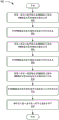
Fig. 5 shows an illustrative flow diagram depicting exemplary operations for protecting a CMOS amplifier, in accordance with some embodiments.
Detailed Description
In the following description, numerous specific details are set forth, such as examples of specific components, circuits, and processes, in order to provide a thorough understanding of the present disclosure. The term "coupled," as used herein, means directly coupled or coupled through one or more intervening components or circuits. Furthermore, in the following description and for purposes of explanation, specific nomenclature and/or details are set forth in order to provide a thorough understanding of the example embodiments. However, it will be apparent to one skilled in the art that these specific details may not be required to practice the exemplary embodiments. In other instances, well-known circuits and devices are shown in block diagram form in order to avoid obscuring the present disclosure. Any of the signals provided on the various buses described herein may be time multiplexed with other signals and provided on one or more common buses. Additionally, the interconnection between circuit elements or software blocks may be shown as buses or as single signal lines. Each of these buses may alternatively be a single signal line, and each of these single signal lines may alternatively be buses, and a single line or bus may represent any one or more of a number of physical or logical mechanisms for communication between components. The exemplary embodiments should not be construed as limited to the particular examples described herein, but rather include within their scope all embodiments defined by the appended claims.
In addition, the detailed description set forth below with respect to the drawings is intended as a description of exemplary embodiments of the present disclosure and is not intended to represent the only embodiments in which the present disclosure may be practiced. The term "exemplary" used throughout this description means "serving as an example, instance, or illustration," and should not necessarily be construed as preferred or advantageous over other embodiments.
Fig. 1 illustrates a wireless device 110 in communication with a wireless communication system 120, according to some demonstrative embodiments. The wireless communication system 120 may be a Long Term Evolution (LTE) system, a Code Division Multiple Access (CDMA) system, a global system for mobile communications (GSM) system, a Wireless Local Area Network (WLAN) system, or some other wireless system. A CDMA system may implement wideband CDMA (wcdma), CDMA 1X, evolution-data optimized (EVDO), time division synchronous CDMA (TD-SCDMA), or some other version of CDMA. For simplicity, fig. 1 shows a wireless communication system 120 that includes two base stations 130 and 132 and a system controller 140. In general, a wireless system may include any number of base stations and any set of network entities.
Fig. 2 shows a block diagram of an exemplary design of wireless device 110 in fig. 1. In this exemplary design, wireless device 110 includes a primary transceiver 220 coupled to a primary antenna 210, a secondary transceiver 222 coupled to a secondary antenna 212, and a data processor/controller 280. The master transceiver 220 includes a number (K) of receivers 230pa through 230pk and a number (K) of transmitters 250pa through 250pk to support multiple frequency bands, multiple radio technologies, carrier aggregation, and so on. The secondary transceiver 222 includes a number (L) of receivers 230sa-230sl and a number (L) of transmitters 250sa-250sl to support multiple frequency bands, multiple radio technologies, carrier aggregation, receive diversity, multiple-input multiple-output (MIMO) transmission from multiple transmit antennas to multiple receive antennas, and so on.
In the exemplary design shown in fig. 2, each receiver 230 (e.g., 230pa-230pk and 230sa-230sl) includes a Low Noise Amplifier (LNA)240 (e.g., 240pa-240pk and 240sa-240sl) and a receive circuit 242 (e.g., 242pa-242pk and 242sa-242 sl). For data reception, the primary antenna 210 receives signals from base stations and/or other transmitter stations and provides received Radio Frequency (RF) signals, which are routed through the antenna interface circuit 224a and presented as input RF signals to selected receivers. The antenna interface circuit 224a may include switches, duplexers, transmit filters, receive filters, matching circuits, and so forth. In some embodiments, antenna interface circuit 224b (shown in dotted lines) may be external to primary transceiver 220. Thus, the LNA240 and/or the Power Amplifier (PA)254 may have inputs and outputs accessible from outside the primary transceiver 220. The following description assumes that receiver 230pa is the selected receiver. Within receiver 230pa, LNA240 pa amplifies the input RF signal and provides an output RF signal. Receive circuitry 242pa downconverts the output RF signal from RF to baseband, amplifies and filters the downconverted signal, and provides an analog input signal to data processor/controller 280. The receive circuit 242pa may include mixers, filters, amplifiers, matching circuits, oscillators, Local Oscillator (LO) generators, phase-locked loops (PLLs), and so forth. Each remaining receiver 230 in the master transceiver 220 may operate in a similar manner as the receiver 230 pa. The receiver 230 and associated antenna interface circuit 226a (or 226b) within the secondary transceiver 222 may operate in a similar manner as the receiver 230 pa.
In the exemplary design shown in fig. 2, each transmitter 250 (e.g., 250PA-250pk and 250sa-250sl) includes a transmit circuit 252 (e.g., 252PA-252pk and 252sa-252sl) and a Power Amplifier (PA)254 (e.g., 254PA-254pk and 254sa-254 sl). For data transmission, data processor/controller 280 processes (e.g., encodes and modulates) the data to be transmitted and provides an analog output signal to the selected transmitter. The following description assumes that transmitter 250pa is the selected transmitter. Within transmitter 250pa, transmit circuitry 252pa amplifies, filters, and upconverts the analog output signal from baseband to RF and provides a modulated RF signal. The transmit circuit 252pa may include amplifiers, filters, mixers, matching circuits, oscillators, LO generators, PLLs, and so forth. The PA 254PA receives and amplifies the modulated RF signal and provides a transmit RF signal having the proper output power level. The transmit RF signal is routed through antenna interface circuit 224a (or antenna interface circuit 224b) and transmitted via main antenna 210. Each remaining transmitter 250 in the master transceiver 220 may operate in a similar manner as transmitter 250 pa. The transmitter 250 and associated antenna interface circuit 226a (or 226b) within the secondary transceiver 222 may operate in a similar manner as the receiver 230 pa.
Each of the receiver 230 and the transmitter 250 may also include other circuitry not shown in fig. 2, such as filters, matching circuits, and so forth. All or portions of transceivers 220 and 222 may be implemented on one or more analog Integrated Circuits (ICs), RF ICs (RFICs), mixed signal ICs, and so forth. For example, as described below, the LNAs 240 and receive circuits 242 within the transceivers 220 and 222 may be implemented on multiple IC chips. The circuitry in transceivers 220 and 222 may also be implemented in other ways.
A data processor/controller 280 may perform various functions for wireless device 110. For example, data processor/controller 280 may perform processing for data received via receiver 230 and data transmitted via transmitter 250. Data processor/controller 280 may control the operation of various circuits within transceivers 220 and 222. A memory 282 may store program codes and data for data processor/controller 280. Data processor/controller 280 may be implemented on one or more Application Specific Integrated Circuits (ASICs) and/or other ICs.
Fig. 3 depicts an exemplary embodiment of a CMOS amplifier 300 according to some embodiments. In some embodiments, the CMOS amplifier 300 may be included within the LNA240, the receive circuit 242, the PA 254, and/or the transmit circuit 252 as described above. CMOS amplifier 300 may amplify signals within wireless device 110, such as modulated RF signals that may be transmitted and/or received. As shown, the CMOS amplifier 300 includes a transistor P1, a transistor N1, a first degeneration inductor 310, a second degeneration inductor 311, a main protection circuit 301 including a protection diode 302 and 303, an auxiliary protection circuit 304 including a protection diode 320 and 324, and a supply clamp (supply clamp) 305. In some embodiments, transistor P1 may be a PMOS transistor and transistor N1 may be an NMOS transistor. The CMOS amplifier 300 may further include an input terminal 340 and an output terminal 341.
Transistor P1 and transistor N1 may be coupled together to form an inverting amplifier for CMOS amplifier 300. For example, the gate terminal of transistor P1 may be coupled to the gate terminal of transistor N1 and may form the input terminal for the inverting amplifier (and input terminal 340 for CMOS amplifier 300). The source terminal of transistor P1 may be coupled to a supply voltage, such as VDD. The source terminal of transistor N1 may be coupled to ground. A drain terminal of transistor P1 may be coupled to a drain terminal of transistor N1 and may form an output terminal for an inverting amplifier (and output terminal 341 for CMOS amplifier 300).
In some embodiments, degeneration inductors 310 and 311 may be coupled to transistor P1 and transistor N1 to reduce (among other things) the dependence of CMOS amplifier 300 on the absolute gain of transistor P1 and/or transistor N1. For example, the absolute gain provided by transistor P1 and/or transistor N1 may be reduced by degeneration inductors 310 and 311, in exchange for providing a more predictable (even lower) gain for CMOS amplifier 300. In some other embodiments, degeneration inductors 310 and 311 may improve linearity associated with CMOS amplifier 300. Thus, the output signal provided by CMOS amplifier 300 may be made more proportional to the input signal provided to the CMOS amplifier by degeneration inductor 310 and/or degeneration inductor 311. In some embodiments, the first degeneration inductor 310 may couple the source terminal of transistor P1 to the supply voltage, and the second degeneration inductor 311 may couple the source terminal of transistor N1 to ground.
The CMOS amplifier 300 may be protected from some ESD events by the primary protection circuit 301, the supply clamp 305, and the auxiliary protection circuit 304. An ESD event may occur when static electricity is received through one or more terminals of CMOS amplifier 300. The voltage associated with the ESD event may be sufficient to damage transistor P1 and/or transistor N1. In some embodiments (e.g., transistors implemented using nano-CMOS technology), a voltage as low as five volts may be sufficient to damage the transistors (e.g., transistor P1 and/or transistor N1). The voltage associated with an ESD event may be 125 volts or more. The primary protection circuit 301, the supply clamp 305, and the auxiliary protection circuit 304 may prevent the transistor P1 and/or the transistor N1 from being exposed to high voltages associated with ESD events.
The main protection circuit 301 may provide a discharge path when a relatively high voltage is received through ground (e.g., via a ground terminal, not shown for simplicity) or through the input terminal 340. The main protection circuit 301 may include a protection diode 302 and a protection diode 303. In some embodiments, receiving a high voltage may be referred to as a Capacitive Discharge Model (CDM) event. For example, when the received high voltage is positive with respect to ground, then the high voltage may be referred to as a negative CDM event. In a similar manner, when the received high voltage is negative with respect to ground, then the high voltage may be referred to as a positive CDM event.
In one embodiment, if a high positive voltage (e.g., a negative CDM event) is received at input terminal 340, protection diode 303 may operate (e.g., be forward biased) and conduct the high positive voltage from input terminal 340 to the supply voltage terminal (e.g., VDD), through supply clamp 305, and to ground. In some embodiments, the voltage supply terminal may be floating and may not provide a discharge current path. The operation of supply clamp 305 is described in more detail below. Thus, when the voltage received at the input terminal 340 is greater than or equal to the forward voltage associated with the protection diode 303, then the protection diode 303 may conduct the voltage at the input terminal 340 to ground. In another embodiment, if a high negative voltage (e.g., a positive CDM event) is received at input terminal 340, protection diode 302 may operate and conduct the high negative voltage through input terminal 340. In some embodiments, the forward voltage associated with the protection diode 302 and/or the protection diode 303 may operate as a threshold voltage for the discharge path provided by the main protection circuit 301. When the voltage exceeds the threshold voltage, protection diode 302 and/or protection diode 303 may provide a discharge path. For example, if a high positive voltage (e.g., a positive CDM event) is received at the ground terminal, the protection diode 302 may operate and conduct the high voltage through the input terminal 340. In this case, the voltage at the ground terminal may be greater than the forward voltage associated with the protection diode 302.
The supply clamp 305 may operate as a clamp circuit and provide a discharge path when a relatively high voltage is received at the supply voltage terminal. In some embodiments, the supply clamp 305 may include a transistor, such as an NMOS transistor (not shown for simplicity), configured to conduct (e.g., turn on) when the voltage at the power supply terminal exceeds a threshold voltage. For example, supply clamp 305 may sense a voltage level at a supply voltage terminal. When the voltage level exceeds a threshold voltage, supply clamp 305 may turn on and conduct voltage from the supply voltage terminal to the ground terminal. In some embodiments, under normal operating conditions, the threshold voltage may be high enough to allow normal operation, but low enough to prevent transistor damage resulting from a relatively high voltage being undesirably applied to CMOS amplifier 300. For example, if the normal operating voltage of CMOS amplifier 300 is 3.3 volts, supply clamp 305 may be configured to turn on when the voltage at the supply voltage terminal reaches or exceeds 4 volts.
The auxiliary protection circuit 304 may protect the selected junction of transistor P1 and transistor N1 from relatively high voltage levels caused by ESD events. In some embodiments, the auxiliary protection circuit 304 may provide additional ESD protection when used in conjunction with the main protection circuit 301 and the supply clamp 305. In some embodiments, additional ESD protection may improve ESD performance in circuits with one or more parasitic inductors and/or resistors. The auxiliary protection circuit 304 may include protection diodes 320 and 324. In one embodiment, the protection diode 320 may protect the transistor P1 by limiting a voltage difference between the gate terminal and the source terminal of the transistor P1. For example, the protection diode 320 may limit a voltage difference between the source terminal and the gate terminal of the transistor P1 to be no greater than a forward voltage associated with the protection diode 320. Accordingly, if a high positive voltage from an ESD event is received at input terminal 340 (e.g., a negative CDM event when the voltage at input terminal 340 is at a higher voltage potential than the supply voltage terminal), protection diode 320 may ensure that the voltage difference between the gate and source terminals of transistor P1 is limited to the forward voltage associated with protection diode 320. In this manner, the protection diode 320 may protect the gate/source junction of the transistor P1.
In one embodiment, protection diodes 321-323 may protect transistor P1 and/or transistor N1 by limiting the voltage difference between the gate terminals and the commonly coupled drain terminals of transistor P1 and transistor N1. If a high positive voltage is received at input terminal 340 (e.g., a negative CDM event when output terminal 341 is at a lower voltage potential than input terminal 340), protection diode 323 may limit the voltage difference between the gate terminals of transistors P1 and N1 and the drain terminals of transistors P1 and N1. Accordingly, if a high positive voltage is received at the input terminal 340 from an ESD event, the protection diode 323 can ensure that the voltage difference between the gate and drain terminals of the transistor P1 and the transistor N1 is limited to the forward voltage associated with the protection diode 323. In some embodiments, protection diode 323 may ensure that a voltage difference between the gate terminal and the source terminal of transistor N1 may be limited to a forward voltage associated with protection diode 323.
In a similar manner, the protection diodes 321 and 322 may also protect the transistor P1 and/or the transistor N1. For example, if a high negative voltage is received at the output terminal 341 (e.g., a positive CDM event when the output terminal 341 is at a higher voltage potential than the input terminal 340), the protection diodes 321-322 may limit the voltage difference between the gate terminals of the transistor P1 and the transistor N1 and the commonly coupled drain terminals of the transistor P1 and the transistor N1. In some embodiments, as shown, protection diodes 321 and 322 may be coupled in series between input terminal 340 and output terminal 341. Accordingly, the voltage difference between the output terminal 341 and the input terminal 340 may be limited to a voltage sum based on the forward voltage associated with the protection diode 321 and the forward voltage associated with the protection diode 322. In this manner, the protection diodes 321-323 can protect the gate/drain junctions of the transistors P1 and N1. In other embodiments, the protection diodes 321-323 can protect the gate/source junction of the transistor P1. In some embodiments, the input terminal 340 may be coupled to gate terminals of transistor P1 and transistor N1. Similarly, output terminal 341 may be coupled to the drain terminals of transistor P1 and transistor N1. Therefore, the protection diodes 321-323 can also limit the voltage difference between the input terminal 340 and the output terminal 341.
In some embodiments, the protection diode 324 may protect the transistor N1 by limiting the voltage difference between the gate terminal and the source terminal of the transistor N1. For example, the protection diode 324 may protect the transistor N1 by limiting the voltage difference between the gate and source terminals of the transistor N1 to be no greater than the forward voltage associated with the protection diode 324. Thus, if a high positive voltage from an ESD event (e.g., a positive CDM event) is received through the ground terminal, protection diode 324 may ensure that the voltage difference between the gate and source terminals of transistor N1 is limited to the forward voltage associated with protection diode 324. In this manner, the protection diode 324 may protect the gate/source junction of transistor N1.
In some embodiments, the auxiliary diode 304 may also protect the transistor P1 and the transistor N1 from voltages that may be induced across parasitic inductors that may be included within the CMOS amplifier 300. For example, CMOS amplifier 300 may include a parasitic inductor 360. Although only one parasitic inductor 360 is shownOne of ordinary skill in the art will recognize that additional parasitic inductors may be included within other circuit branches of CMOS amplifier 300. If a relatively large voltage associated with an ESD event is coupled to the input terminal 340, the relatively large voltage may be induced across the parasitic inductor 360 in response to a rapid change in current flow resulting from the ESD event. Because the time associated with an ESD event may be quite small, the induced voltage across the parasitic inductor may be large (e.g., ). In some embodiments, the voltage induced across the
 parasitic inductor 360 may cause potentially damaging voltages between the gate and source terminals of transistor N1 and between the gate and source terminals of transistor P1. In some cases, the auxiliary diode 304 may limit the magnitude of the voltage between the terminals of transistor P1 and transistor N1 (including the voltage caused by one or more parasitic inductors within the CMOS amplifier 300).
Fig. 4 depicts another exemplary embodiment of a CMOS amplifier 400 according to some embodiments. CMOS amplifier 400 may be similar to CMOS amplifier 300, but may include one or more additional elements. For example, the CMOS amplifier 400 may include a transistor P1, a transistor N1, a first degeneration inductor 310, a second degeneration inductor 311, a main protection circuit 301, an auxiliary protection circuit 304, and a supply clamp 305 in common with the CMOS amplifier 300. Additionally, the CMOS amplifier 400 may include one or more resistors 402 and 404 in series with one or more protection diodes. In one embodiment, resistor 402 may be coupled in series with protection diode 320, resistor 403 may be coupled in series with protection diode 323, and resistor 404 may be coupled in series with protection diode 324. In some embodiments, other numbers of resistors may be included with protection diodes 320 and 324 and/or protection diodes 302 and 303. For example, a resistor may be coupled in series with the protection diode 321, and/or a second resistor may be coupled with one of the resistors 402 and 404 (not shown for simplicity). In still other embodiments, one or more of resistors 402-404 may be omitted.
Resistors 402-404 may be combined with associated protection diodes to enable the additional voltage to be dissipated. For example, protection diode 320 and resistor 402 may limit the voltage difference between the gate and source terminals of transistor P1 to the forward voltage associated with protection diode 320 and the associated voltage across resistor 402. In a similar manner, resistor 403 and protection diode 323 may limit the voltage difference between the gate and drain terminals of transistor P1 and transistor N1, and resistor 404 and protection diode 324 may limit the voltage difference between the source and gate terminals of the N1 transistor. In some embodiments, the resistance values for resistors 402-404 may range from 1 to 5 ohms, although other suitable resistance values may be used.
Fig. 5 shows an illustrative flow diagram depicting example operations 500 for protecting a CMOS amplifier, in accordance with some embodiments. Some embodiments may perform the operations described herein with additional operations, fewer operations, operations in a different order, operations in parallel, and/or with some operations differently. Referring also to fig. 2 and 3, a first protection diode is coupled between the gate terminal and the source terminal of PMOS transistor P1 of CMOS amplifier 300 (502). In some embodiments, the first protection diode may include a protection diode 320 (see fig. 3). Next, the voltage difference between the gate terminal and the source terminal of the transistor P1 is limited (504). In some embodiments, the voltage difference may be limited to a forward voltage associated with the first protection diode. In other embodiments, for example, when the gate terminal of transistor P1 is coupled to the input terminal of CMOS amplifier 300 and the source terminal of transistor P1 is coupled to the supply voltage, the first protection diode may limit the voltage difference between the input of CMOS amplifier 300 and the supply voltage. In some embodiments, degeneration inductor 310 may be coupled between the source terminal of transistor P1 and the supply voltage. Degeneration inductor 310 may reduce the dependence of CMOS amplifier 300 on the absolute gain of transistor P1.
Next, a second protection diode is coupled between the gate terminal and the drain terminal of transistor P1 (506). In some embodiments, the second protection diode may include a protection diode 323 (see fig. 3). In other embodiments, the second protection diode may include protection diodes 321 and 322. In still other embodiments, the second protection diode may comprise protection diodes 321-323. Next, the voltage difference between the gate terminal and the drain terminal of the transistor P1 is limited (508).
In some embodiments, the voltage difference between the input terminal and the output terminal of the CMOS amplifier 300 may also be limited. For example, when the input terminal 340 of the CMOS amplifier 300 is coupled to the gate terminal of the transistor P1 and the output terminal 341 of the CMOS amplifier 300 is coupled to the drain terminal of the transistor P1, then the voltage difference between the input terminal 340 and the output terminal 341 of the CMOS amplifier 300 may be limited.
Next, a third protection diode is coupled between the source terminal and the gate terminal of the NMOS transistor N1 of the CMOS amplifier 300 (510). In one embodiment, the third protection diode may include the protection diode 324. Next, the voltage difference between the source terminal and the gate terminal of the transistor N1 is limited (512). In some embodiments, the voltage difference may be limited to a forward voltage associated with the third protection diode. In other embodiments, for example, when the gate terminal of transistor N1 is coupled to input terminal 340 and the source terminal of transistor N1 is coupled to ground, the third protection diode may limit the voltage difference between ground and input terminal 340 of CMOS amplifier 300. In some embodiments, degeneration inductor 311 may be coupled between the source terminal of transistor N1 and ground. Degeneration inductor 311 may reduce the dependence of CMOS amplifier 300 on the absolute gain of transistor N1.
Next, an output signal is generated by the CMOS amplifier 300 based on the input signal (514). For example, an input signal may be received at input terminal 340 of CMOS amplifier 300. The input signal may be amplified by transistor P1 and/or transistor N1. Transistor P1 and/or transistor N1 may generate output signals for CMOS amplifier 300 via output terminal 341.
The various illustrative logical blocks, modules, and circuits described in connection with the embodiments disclosed herein may be implemented or performed with the following designed to perform the functions described herein: a general purpose processor, a Digital Signal Processor (DSP), an Application Specific Integrated Circuit (ASIC), a Field Programmable Gate Array (FPGA) or other programmable logic device, discrete gate or transistor logic, discrete hardware components, or any combination thereof. A general purpose processor may be a microprocessor, but in the alternative, the processor may be any conventional processor, controller, microcontroller, or state machine. A processor may also be implemented as a combination of computing devices, e.g., a combination of a DSP and a microprocessor, a plurality of microprocessors, one or more microprocessors in conjunction with a DSP core, or any other such configuration.
In one or more exemplary embodiments, the functions described may be implemented in hardware, software, firmware, or any combination thereof. If implemented in software, the functions may be stored on or transmitted over as one or more instructions or code on a computer-readable medium. Computer-readable media includes both computer storage media and communication media including any medium that facilitates transfer of a computer program from one place to another. A storage media may be any available media that can be accessed by a computer. By way of example, and not limitation, such computer-readable media can comprise RAM, ROM, EEPROM, CD-ROM or other optical disk storage, magnetic disk storage or other magnetic storage devices, or any other medium that can be used to carry or store desired program code in the form of instructions or data structures and that can be accessed by a computer. Further, any connection is properly termed a computer-readable medium. For example, if the software is transmitted from a website, server, or other remote source using a coaxial cable, fiber optic cable, twisted pair, Digital Subscriber Line (DSL), or wireless technologies such as infrared, radio, and microwave, then the coaxial cable, fiber optic cable, twisted pair, DSL, or wireless technologies such as infrared, radio, and microwave are included in the definition of medium. Disk and disc, as used herein, includes Compact Disc (CD), laser disc, optical disc, Digital Versatile Disc (DVD), floppy disk and blu-ray disc where disks usually reproduce data magnetically, while discs reproduce data optically with lasers. Combinations of the above should also be included within the scope of computer-readable media.
In the foregoing specification, exemplary embodiments have been described with reference to specific exemplary embodiments thereof. It will, however, be evident that various modifications and changes may be made thereto without departing from the broader scope of the disclosure as set forth in the appended claims. The specification and drawings are, accordingly, to be regarded in an illustrative sense rather than a restrictive sense.
Claims (18)
1. An apparatus for an amplifier, comprising:
a PMOS transistor configured to amplify an input signal and generate an output signal of the amplifier;
a degeneration inductor configured to reduce a gain of the amplifier;
a first protection diode configured to limit a voltage difference between an input terminal of the amplifier and a supply voltage;
one or more main protection diodes configured to limit a voltage difference between ground and the supply voltage when the voltage difference between ground and the supply voltage exceeds a first threshold voltage; and
a clamp circuit configured to limit a voltage difference between the supply voltage and ground when the voltage difference exceeds a second threshold voltage.
2. The apparatus of claim 1, wherein the first protection diode is further configured to limit a voltage difference between a gate terminal and a source terminal of the PMOS transistor.
3. The apparatus of claim 1, wherein the first protection diode is coupled between a source terminal of the PMOS transistor and a gate terminal of the PMOS transistor.
4. The apparatus of claim 1, wherein the first protection diode is further configured to protect a gate/source junction of the PMOS transistor.
5. The apparatus of claim 1, further comprising:
a resistor coupled in series with the first protection diode.
6. The apparatus of claim 1, wherein the degeneration inductor is coupled between a source terminal of the PMOS transistor and the supply voltage.
7. The apparatus of claim 1, further comprising:
a second protection diode configured to limit a voltage difference between the input terminal of the amplifier and an output terminal of the amplifier.
8. The apparatus of claim 7, wherein the second protection diode is further configured to limit a voltage difference between a gate terminal of the PMOS transistor and a drain terminal of the PMOS transistor.
9. The apparatus of claim 7, wherein the second protection diode is coupled between a gate terminal of the PMOS transistor and a drain terminal of the PMOS transistor.
10. The apparatus of claim 1, further comprising:
an NMOS transistor configured to generate the output signal of the amplifier based on the input signal, wherein the amplifier is a CMOS amplifier.
11. The apparatus of claim 10, further comprising:
a third protection diode configured to limit a voltage difference between the input terminal of the amplifier and a source terminal of the NMOS transistor.
12. An apparatus for an amplifier, comprising:
means for amplifying an input signal via a PMOS transistor and generating an output signal of the amplifier;
means for reducing a gain of the amplifier;
means for limiting a voltage difference between an input terminal of the amplifier and a supply voltage;
means for limiting a voltage difference between ground and the supply voltage when the voltage difference exceeds a first threshold voltage; and
means for limiting a voltage difference between the supply voltage and ground when the voltage difference exceeds a second threshold voltage.
13. The apparatus of claim 12, wherein the means for limiting the voltage difference also limits a voltage difference between a gate terminal and a source terminal of the PMOS transistor.
14. The apparatus of claim 12, further comprising:
means for limiting a voltage difference between the input terminal of the amplifier and an output terminal of the amplifier.
15. The apparatus of claim 14, wherein the means for limiting the voltage difference also limits a voltage between a gate terminal and a drain terminal of the PMOS transistor.
16. The apparatus of claim 12, wherein the means for amplifying the input signal and generating the output signal of the amplifier is to limit a voltage difference between the input terminal of the amplifier and a source terminal of an NMOS transistor, and wherein the amplifier is a CMOS amplifier.
17. A method for an amplifier, comprising:
amplifying an input signal by a PMOS transistor and generating an output signal of the amplifier;
reducing a gain of the amplifier by an inductor;
limiting a voltage difference between an input terminal of the amplifier and a supply voltage by a first protection diode;
limiting, by one or more main protection diodes, a voltage difference between ground and the supply voltage when the voltage difference exceeds a first threshold voltage; and
limiting, by a clamp circuit, a voltage difference between the supply voltage and ground when the voltage difference exceeds a second threshold voltage.
18. The method of claim 17, wherein limiting the voltage difference comprises:
limiting a voltage difference between a gate terminal and a source terminal of the PMOS transistor.
Applications Claiming Priority (3)
| Application Number | Priority Date | Filing Date | Title |
|---|---|---|---|
| US14/632,646 US9559640B2 (en) | 2015-02-26 | 2015-02-26 | Electrostatic discharge protection for CMOS amplifier |
| US14/632,646 | 2015-02-26 | ||
| PCT/US2016/015235 WO2016137648A1 (en) | 2015-02-26 | 2016-01-27 | Electrostatic discharge protection for cmos amplifier |
Publications (2)
| Publication Number | Publication Date |
|---|---|
| CN107258054A CN107258054A (en) | 2017-10-17 |
| CN107258054B true CN107258054B (en) | 2021-01-12 |
Family
ID=55359737
Family Applications (1)
| Application Number | Title | Priority Date | Filing Date |
|---|---|---|---|
| CN201680011537.5A Active CN107258054B (en) | 2015-02-26 | 2016-01-27 | Apparatus and method for amplifier |
Country Status (7)
| Country | Link |
|---|---|
| US (1) | US9559640B2 (en) |
| EP (1) | EP3262753A1 (en) |
| JP (1) | JP2018510560A (en) |
| KR (1) | KR20170123313A (en) |
| CN (1) | CN107258054B (en) |
| BR (1) | BR112017018320A2 (en) |
| WO (1) | WO2016137648A1 (en) |
Families Citing this family (3)
| Publication number | Priority date | Publication date | Assignee | Title |
|---|---|---|---|---|
| EP3367562A1 (en) | 2017-02-22 | 2018-08-29 | Comet AG | High power amplifier circuit with protective feedback circuit |
| US10797656B2 (en) * | 2018-08-06 | 2020-10-06 | Analong Devices Global Unlimited Company | Breakdown protection circuit for power amplifier |
| US10951177B1 (en) * | 2019-06-05 | 2021-03-16 | Rockwell Collins, Inc. | Radio frequency power limiter with reflected power detection |
Citations (6)
| Publication number | Priority date | Publication date | Assignee | Title |
|---|---|---|---|---|
| CN101039027A (en) * | 2007-05-10 | 2007-09-19 | 北京中星微电子有限公司 | Improved electrostatic discharge protecting circuit |
| US7649722B2 (en) * | 2005-09-14 | 2010-01-19 | Interuniversitair Microelektronica Centrum (Imec) | Electrostatic discharge protected circuits |
| CN101859766A (en) * | 2009-04-13 | 2010-10-13 | 苏州芯美微电子科技有限公司 | Novel NMOS (N-channel Metal Oxide Semiconductor) clamping between power VDD (Voltage Drain Drain) and IO (Input/Output) pin and application method thereof |
| US7978454B1 (en) * | 2007-08-01 | 2011-07-12 | National Semiconductor Corporation | ESD structure that protects against power-on and power-off ESD event |
| CN102204087A (en) * | 2008-10-29 | 2011-09-28 | 高通股份有限公司 | Amplifier with improved ESD protection circuitry |
| CN102255300A (en) * | 2010-05-20 | 2011-11-23 | 台湾积体电路制造股份有限公司 | RF assembly |
Family Cites Families (10)
| Publication number | Priority date | Publication date | Assignee | Title |
|---|---|---|---|---|
| US4250463A (en) * | 1978-08-14 | 1981-02-10 | Telex Computer Products, Inc. | Overload protection to prevent saturation of video amplifiers |
| US5740000A (en) | 1996-09-30 | 1998-04-14 | Hewlett-Packard Co. | ESD protection system for an integrated circuit with multiple power supply networks |
| ITMI20040871A1 (en) * | 2004-04-30 | 2004-07-30 | St Microelectronics Srl | LOW NOISE AMPLIFIER |
| US8476709B2 (en) | 2006-08-24 | 2013-07-02 | Infineon Technologies Ag | ESD protection device and method |
| US8000068B2 (en) | 2008-10-27 | 2011-08-16 | Qualcomm Incorporated | ESD protection for field effect transistors of analog input circuits |
| US7902604B2 (en) | 2009-02-09 | 2011-03-08 | Alpha & Omega Semiconductor, Inc. | Configuration of gate to drain (GD) clamp and ESD protection circuit for power device breakdown protection |
| TWI463792B (en) | 2009-10-29 | 2014-12-01 | Novatek Microelectronics Corp | Amplifier circuit with overshoot suppression |
| US8605396B2 (en) | 2011-01-07 | 2013-12-10 | Taiwan Semiconductor Manufacturing Company, Ltd. | ESD protection devices and methods for forming ESD protection devices |
| JP6243720B2 (en) | 2013-02-06 | 2017-12-06 | エスアイアイ・セミコンダクタ株式会社 | Semiconductor device provided with ESD protection circuit |
| US9929698B2 (en) | 2013-03-15 | 2018-03-27 | Qualcomm Incorporated | Radio frequency integrated circuit (RFIC) charged-device model (CDM) protection |
-
2015
- 2015-02-26 US US14/632,646 patent/US9559640B2/en active Active
-
2016
- 2016-01-27 KR KR1020177023548A patent/KR20170123313A/en unknown
- 2016-01-27 BR BR112017018320A patent/BR112017018320A2/en not_active Application Discontinuation
- 2016-01-27 JP JP2017544896A patent/JP2018510560A/en active Pending
- 2016-01-27 WO PCT/US2016/015235 patent/WO2016137648A1/en active Application Filing
- 2016-01-27 EP EP16704750.5A patent/EP3262753A1/en not_active Withdrawn
- 2016-01-27 CN CN201680011537.5A patent/CN107258054B/en active Active
Patent Citations (6)
| Publication number | Priority date | Publication date | Assignee | Title |
|---|---|---|---|---|
| US7649722B2 (en) * | 2005-09-14 | 2010-01-19 | Interuniversitair Microelektronica Centrum (Imec) | Electrostatic discharge protected circuits |
| CN101039027A (en) * | 2007-05-10 | 2007-09-19 | 北京中星微电子有限公司 | Improved electrostatic discharge protecting circuit |
| US7978454B1 (en) * | 2007-08-01 | 2011-07-12 | National Semiconductor Corporation | ESD structure that protects against power-on and power-off ESD event |
| CN102204087A (en) * | 2008-10-29 | 2011-09-28 | 高通股份有限公司 | Amplifier with improved ESD protection circuitry |
| CN101859766A (en) * | 2009-04-13 | 2010-10-13 | 苏州芯美微电子科技有限公司 | Novel NMOS (N-channel Metal Oxide Semiconductor) clamping between power VDD (Voltage Drain Drain) and IO (Input/Output) pin and application method thereof |
| CN102255300A (en) * | 2010-05-20 | 2011-11-23 | 台湾积体电路制造股份有限公司 | RF assembly |
Also Published As
| Publication number | Publication date |
|---|---|
| WO2016137648A1 (en) | 2016-09-01 |
| US9559640B2 (en) | 2017-01-31 |
| JP2018510560A (en) | 2018-04-12 |
| US20160254789A1 (en) | 2016-09-01 |
| CN107258054A (en) | 2017-10-17 |
| KR20170123313A (en) | 2017-11-07 |
| EP3262753A1 (en) | 2018-01-03 |
| BR112017018320A2 (en) | 2018-04-17 |
Similar Documents
| Publication | Publication Date | Title |
|---|---|---|
| US9106072B2 (en) | Electrostatic discharge protection of amplifier cascode devices | |
| CN106463953B (en) | Biasing techniques and circuit arrangements for reducing leakage current in circuits | |
| US20160036392A1 (en) | Dual-band amplifier | |
| US20180175803A1 (en) | Radio frequency integrated circuit (rfic) charged-device model (cdm) protection | |
| US9407226B2 (en) | Gain control in complementary common gate and common source amplifiers | |
| US9509256B2 (en) | Linearized gate capacitance in power amplifiers | |
| KR102461243B1 (en) | Differential cascode amplifier with selectively coupled gate terminals | |
| CN107258054B (en) | Apparatus and method for amplifier | |
| CN107112957B (en) | Receiver front-end architecture for in-band carrier aggregation | |
| US20140268446A1 (en) | Radio frequency integrated circuit (rfic) charged-device model (cdm) protection | |
| US9425853B2 (en) | Amplifier utilizing a configurable interface to a front end module | |
| US20230253346A1 (en) | Switch with electrostatic discharge (esd) protection | |
| US9473085B2 (en) | Input switch leakage compensation | |
| US20170063306A1 (en) | Gate induced drain leakage reduction | |
| US9385672B2 (en) | Compensated common-mode feedback for an amplifier |
Legal Events
| Date | Code | Title | Description |
|---|---|---|---|
| PB01 | Publication | ||
| PB01 | Publication | ||
| SE01 | Entry into force of request for substantive examination | ||
| SE01 | Entry into force of request for substantive examination | ||
| GR01 | Patent grant | ||
| GR01 | Patent grant |