CN107250344B - Self-locking photoelectric tweezers and manufacture thereof - Google Patents
Self-locking photoelectric tweezers and manufacture thereof Download PDFInfo
- Publication number
- CN107250344B CN107250344B CN201580055791.0A CN201580055791A CN107250344B CN 107250344 B CN107250344 B CN 107250344B CN 201580055791 A CN201580055791 A CN 201580055791A CN 107250344 B CN107250344 B CN 107250344B
- Authority
- CN
- China
- Prior art keywords
- cells
- chamber
- doped
- ring
- channel contains
- Prior art date
- Legal status (The legal status is an assumption and is not a legal conclusion. Google has not performed a legal analysis and makes no representation as to the accuracy of the status listed.)
- Active
Links
Images


Classifications
-
- B—PERFORMING OPERATIONS; TRANSPORTING
- B01—PHYSICAL OR CHEMICAL PROCESSES OR APPARATUS IN GENERAL
- B01L—CHEMICAL OR PHYSICAL LABORATORY APPARATUS FOR GENERAL USE
- B01L3/00—Containers or dishes for laboratory use, e.g. laboratory glassware; Droppers
- B01L3/50—Containers for the purpose of retaining a material to be analysed, e.g. test tubes
- B01L3/502—Containers for the purpose of retaining a material to be analysed, e.g. test tubes with fluid transport, e.g. in multi-compartment structures
- B01L3/5027—Containers for the purpose of retaining a material to be analysed, e.g. test tubes with fluid transport, e.g. in multi-compartment structures by integrated microfluidic structures, i.e. dimensions of channels and chambers are such that surface tension forces are important, e.g. lab-on-a-chip
- B01L3/502761—Containers for the purpose of retaining a material to be analysed, e.g. test tubes with fluid transport, e.g. in multi-compartment structures by integrated microfluidic structures, i.e. dimensions of channels and chambers are such that surface tension forces are important, e.g. lab-on-a-chip specially adapted for handling suspended solids or molecules independently from the bulk fluid flow, e.g. for trapping or sorting beads, for physically stretching molecules
-
- C—CHEMISTRY; METALLURGY
- C12—BIOCHEMISTRY; BEER; SPIRITS; WINE; VINEGAR; MICROBIOLOGY; ENZYMOLOGY; MUTATION OR GENETIC ENGINEERING
- C12M—APPARATUS FOR ENZYMOLOGY OR MICROBIOLOGY; APPARATUS FOR CULTURING MICROORGANISMS FOR PRODUCING BIOMASS, FOR GROWING CELLS OR FOR OBTAINING FERMENTATION OR METABOLIC PRODUCTS, i.e. BIOREACTORS OR FERMENTERS
- C12M1/00—Apparatus for enzymology or microbiology
- C12M1/42—Apparatus for the treatment of microorganisms or enzymes with electrical or wave energy, e.g. magnetism, sonic waves
-
- B—PERFORMING OPERATIONS; TRANSPORTING
- B01—PHYSICAL OR CHEMICAL PROCESSES OR APPARATUS IN GENERAL
- B01L—CHEMICAL OR PHYSICAL LABORATORY APPARATUS FOR GENERAL USE
- B01L3/00—Containers or dishes for laboratory use, e.g. laboratory glassware; Droppers
- B01L3/50—Containers for the purpose of retaining a material to be analysed, e.g. test tubes
- B01L3/502—Containers for the purpose of retaining a material to be analysed, e.g. test tubes with fluid transport, e.g. in multi-compartment structures
- B01L3/5027—Containers for the purpose of retaining a material to be analysed, e.g. test tubes with fluid transport, e.g. in multi-compartment structures by integrated microfluidic structures, i.e. dimensions of channels and chambers are such that surface tension forces are important, e.g. lab-on-a-chip
- B01L3/502707—Containers for the purpose of retaining a material to be analysed, e.g. test tubes with fluid transport, e.g. in multi-compartment structures by integrated microfluidic structures, i.e. dimensions of channels and chambers are such that surface tension forces are important, e.g. lab-on-a-chip characterised by the manufacture of the container or its components
-
- B—PERFORMING OPERATIONS; TRANSPORTING
- B01—PHYSICAL OR CHEMICAL PROCESSES OR APPARATUS IN GENERAL
- B01L—CHEMICAL OR PHYSICAL LABORATORY APPARATUS FOR GENERAL USE
- B01L3/00—Containers or dishes for laboratory use, e.g. laboratory glassware; Droppers
- B01L3/50—Containers for the purpose of retaining a material to be analysed, e.g. test tubes
- B01L3/502—Containers for the purpose of retaining a material to be analysed, e.g. test tubes with fluid transport, e.g. in multi-compartment structures
- B01L3/5027—Containers for the purpose of retaining a material to be analysed, e.g. test tubes with fluid transport, e.g. in multi-compartment structures by integrated microfluidic structures, i.e. dimensions of channels and chambers are such that surface tension forces are important, e.g. lab-on-a-chip
- B01L3/502715—Containers for the purpose of retaining a material to be analysed, e.g. test tubes with fluid transport, e.g. in multi-compartment structures by integrated microfluidic structures, i.e. dimensions of channels and chambers are such that surface tension forces are important, e.g. lab-on-a-chip characterised by interfacing components, e.g. fluidic, electrical, optical or mechanical interfaces
-
- B—PERFORMING OPERATIONS; TRANSPORTING
- B03—SEPARATION OF SOLID MATERIALS USING LIQUIDS OR USING PNEUMATIC TABLES OR JIGS; MAGNETIC OR ELECTROSTATIC SEPARATION OF SOLID MATERIALS FROM SOLID MATERIALS OR FLUIDS; SEPARATION BY HIGH-VOLTAGE ELECTRIC FIELDS
- B03C—MAGNETIC OR ELECTROSTATIC SEPARATION OF SOLID MATERIALS FROM SOLID MATERIALS OR FLUIDS; SEPARATION BY HIGH-VOLTAGE ELECTRIC FIELDS
- B03C5/00—Separating dispersed particles from liquids by electrostatic effect
- B03C5/005—Dielectrophoresis, i.e. dielectric particles migrating towards the region of highest field strength
-
- B—PERFORMING OPERATIONS; TRANSPORTING
- B03—SEPARATION OF SOLID MATERIALS USING LIQUIDS OR USING PNEUMATIC TABLES OR JIGS; MAGNETIC OR ELECTROSTATIC SEPARATION OF SOLID MATERIALS FROM SOLID MATERIALS OR FLUIDS; SEPARATION BY HIGH-VOLTAGE ELECTRIC FIELDS
- B03C—MAGNETIC OR ELECTROSTATIC SEPARATION OF SOLID MATERIALS FROM SOLID MATERIALS OR FLUIDS; SEPARATION BY HIGH-VOLTAGE ELECTRIC FIELDS
- B03C5/00—Separating dispersed particles from liquids by electrostatic effect
- B03C5/02—Separators
- B03C5/022—Non-uniform field separators
- B03C5/026—Non-uniform field separators using open-gradient differential dielectric separation, i.e. using electrodes of special shapes for non-uniform field creation, e.g. Fluid Integrated Circuit [FIC]
-
- G—PHYSICS
- G02—OPTICS
- G02B—OPTICAL ELEMENTS, SYSTEMS OR APPARATUS
- G02B21/00—Microscopes
- G02B21/32—Micromanipulators structurally combined with microscopes
-
- B—PERFORMING OPERATIONS; TRANSPORTING
- B01—PHYSICAL OR CHEMICAL PROCESSES OR APPARATUS IN GENERAL
- B01L—CHEMICAL OR PHYSICAL LABORATORY APPARATUS FOR GENERAL USE
- B01L2200/00—Solutions for specific problems relating to chemical or physical laboratory apparatus
- B01L2200/06—Fluid handling related problems
- B01L2200/0647—Handling flowable solids, e.g. microscopic beads, cells, particles
- B01L2200/0668—Trapping microscopic beads
-
- B—PERFORMING OPERATIONS; TRANSPORTING
- B01—PHYSICAL OR CHEMICAL PROCESSES OR APPARATUS IN GENERAL
- B01L—CHEMICAL OR PHYSICAL LABORATORY APPARATUS FOR GENERAL USE
- B01L2400/00—Moving or stopping fluids
- B01L2400/04—Moving fluids with specific forces or mechanical means
- B01L2400/0403—Moving fluids with specific forces or mechanical means specific forces
- B01L2400/0454—Moving fluids with specific forces or mechanical means specific forces radiation pressure, optical tweezers
-
- B—PERFORMING OPERATIONS; TRANSPORTING
- B03—SEPARATION OF SOLID MATERIALS USING LIQUIDS OR USING PNEUMATIC TABLES OR JIGS; MAGNETIC OR ELECTROSTATIC SEPARATION OF SOLID MATERIALS FROM SOLID MATERIALS OR FLUIDS; SEPARATION BY HIGH-VOLTAGE ELECTRIC FIELDS
- B03C—MAGNETIC OR ELECTROSTATIC SEPARATION OF SOLID MATERIALS FROM SOLID MATERIALS OR FLUIDS; SEPARATION BY HIGH-VOLTAGE ELECTRIC FIELDS
- B03C2201/00—Details of magnetic or electrostatic separation
- B03C2201/26—Details of magnetic or electrostatic separation for use in medical applications
-
- C—CHEMISTRY; METALLURGY
- C12—BIOCHEMISTRY; BEER; SPIRITS; WINE; VINEGAR; MICROBIOLOGY; ENZYMOLOGY; MUTATION OR GENETIC ENGINEERING
- C12M—APPARATUS FOR ENZYMOLOGY OR MICROBIOLOGY; APPARATUS FOR CULTURING MICROORGANISMS FOR PRODUCING BIOMASS, FOR GROWING CELLS OR FOR OBTAINING FERMENTATION OR METABOLIC PRODUCTS, i.e. BIOREACTORS OR FERMENTERS
- C12M3/00—Tissue, human, animal or plant cell, or virus culture apparatus
-
- G—PHYSICS
- G01—MEASURING; TESTING
- G01N—INVESTIGATING OR ANALYSING MATERIALS BY DETERMINING THEIR CHEMICAL OR PHYSICAL PROPERTIES
- G01N15/00—Investigating characteristics of particles; Investigating permeability, pore-volume, or surface-area of porous materials
- G01N15/10—Investigating individual particles
-
- G—PHYSICS
- G01—MEASURING; TESTING
- G01N—INVESTIGATING OR ANALYSING MATERIALS BY DETERMINING THEIR CHEMICAL OR PHYSICAL PROPERTIES
- G01N35/00—Automatic analysis not limited to methods or materials provided for in any single one of groups G01N1/00 - G01N33/00; Handling materials therefor
- G01N35/10—Devices for transferring samples or any liquids to, in, or from, the analysis apparatus, e.g. suction devices, injection devices
- G01N2035/1027—General features of the devices
- G01N2035/1034—Transferring microquantities of liquid
- G01N2035/1046—Levitated, suspended drops
Abstract
A novel self-locking optoelectronic tweezers (SLOT) for single microparticle manipulation over large areas is provided. The DEP force generated by the annular lateral phototransistor is used to lock single particles or cells in the dark state. The locked particles or cells may be selectively released by optically deactivating the locking sites.
Description
Cross Reference to Related Applications
This application claims the benefits and priority of USSN 62/038,150 filed on day 8,15 of 2014 and USSN 62/181,627 filed on day 6, 18 of 2015, both of which are incorporated herein by reference in their entireties for all purposes.
Statement of government support
The present invention was made with government support under grant number 1232279 awarded by the National Science Foundation. The government has certain rights in the invention.
Background
Optoelectronic tweezers (OET) have been developed for the parallel manipulation of single cells and particles for various biological applications (Chiou et al (2005) Nature 436(7049): 370-. For example, optoelectronic tweezers (OET) have been developed for dynamic manipulation of single cells and particles (Chiou et al (2005) Nature,436(7049): 370-. OET can be used to capture and manipulate semiconductor and metal nanowires (Jamshidi et al (2008) Nature Photonics,2(2):86-89), micro/nanobeads (Ota et al 92013) Nano letters, 13(6): 2766-2770; glaesener et al (2012) Optics letters, 37(18): 3744-3746; Zaarowna-Dabrowska et al (2011) Optics Express,19(3): 2720-; shah et al (2009) Lab on a Chip,9(12): 1732-.
In a typical OET setup, 1mm in a low conductivity medium (0.01S/m)2A large number (e.g., over 15,000) of individually addressable optical traps may be formed over the area. However, the utility of OET suffers from bottlenecks due to its incompatibility with physiological buffers and low handling flux. Previously, OET based vertical phototransistors (Hsu et al (2010) Lab on a Chip,10(2):165-172) have been proposed to solve the buffer incompatibility problem. However, low throughput remains a major problem for all optical manipulation techniques, including but not limited to OET. This fundamental limitation comes from the trade-off between field of view (FOV) and optical resolution. A large FOV typically means using a lens with a low numerical aperture (n.a.). However, such low numerical aperture lenses do not provide the required optical image clarity to create light intensity gradients that produce sufficient trapping force. This is true for both direct optical forces in optical tweezers and light induced DEP forces in OETs. Therefore, large area optical manipulation of single cells or particles is almost impossible even with high power beams.
Disclosure of Invention
Various embodiments contemplated herein may include, but are not limited to, one or more of the following:
embodiment 1: a self-locking optoelectronic tweezers device, comprising: a first substrate comprising a first electrode and a plurality of ring-shaped and/or non-circular phototransistors that can be optically turned on and off, wherein the phototransistors and the first substrate are configured to generate a negative Dielectrophoretic (DEP) force at the ring-shaped or non-circular phototransistors upon application of a voltage to the device; and turning off DEP at a ring-or bean-shaped (e.g., kidney bean-shaped) phototransistor when the phototransistor is illuminated with light; and a surface comprising a second electrode, wherein the surface is arranged to define a chamber or channel between the first substrate and the surface, and the chamber or channel is configured to receive and, or hold, a fluid containing cells or particles.
Embodiment 2: the device of embodiment 1, wherein the phototransistor is ring-shaped.
Embodiment 3: the apparatus of embodiment 1, wherein the non-circular phototransistor is bean-shaped (e.g., kidney bean-shaped).
Embodiment 4: the apparatus of embodiments 1-3, wherein the phototransistor generates an electric field perpendicular to the plane of the device.
Embodiment 5: the device of embodiments 1-4, wherein the annular or non-circular portion of the phototransistor is p-doped.
Embodiment 6: the device of embodiments 1-5, wherein the substrate is a doped p-type substrate comprising a ring-shaped or bean-shaped portion, wherein the center of the ring-shaped or bean-shaped portion and a region outside the ring-shaped or non-circular portion are n-doped.
Embodiment 7: the device of embodiment 6, wherein the doped p-type substrate is a doped p-type group III-V or p-type group IV material.
Embodiment 8: the device of embodiment 6, wherein the doped p-type substrate is doped p-type silicon.
Embodiment 9: the device of embodiment 6, wherein the n-doped region is coated with a thin film conductor.
Embodiment 10: the device of embodiment 9, wherein one or more of the thin film conductors comprises a material selected from the group consisting of Au, Ti, Al, Cr, Ni, Ta, Pd, and Pt.
Embodiment 11: the device of embodiment 1, wherein the annular or non-circular portion of the phototransistor is n-doped.
Embodiment 12: the device of embodiments 1 and 6, wherein the substrate is a doped n-type substrate comprising an annular or non-circular portion, wherein the center of the annular or non-circular portion and the region outside the annular or non-circular portion are p-doped.
Embodiment 13: the device of embodiment 12, wherein the doped n-type substrate is a doped n-type group III-V or n-type group IV material.
Embodiment 14: the device of embodiment 12, wherein the doped n-type substrate is doped n-type silicon.
Embodiment 15: the device of embodiment 12, wherein the p-doped region is coated with a thin film conductor.
Embodiment 16: the apparatus of embodiment 15, wherein one or more of the thin film conductors comprises a material selected from the group consisting of Au, Ti, Al, Cr, Ni, Ta, Pd, and Pt.
Embodiment 17: the device of embodiments 1-15 wherein a top surface of the substrate is coated with an insulator having an opening to the conductor film at the center of the annular or non-circular shape.
Embodiment 18: the device of embodiment 17, wherein the insulator comprises a material selected from the group consisting of SU-8 or other photoresist, PDMS, silicon dioxide, Al2O3And silicon nitride.
Embodiment 19: the device of embodiments 17-18, wherein the insulating layer is configured to provide about 50% partial voltage leakage in the dark state.
Embodiment 20: the device of embodiments 17-19, wherein the insulator comprises Al2O3。
Embodiment 21: the apparatus of embodiment 20, wherein the Al of the insulator is included2O3The thickness of the layer is about 30 nm.
Embodiment 22: the apparatus of embodiments 1-21, wherein the substrate ranges in size from about 1mm2Or about 5mm2Or about 10mm2Or about 50mm2Or about 1cm2Up to about 500cm2Or up to about 200cm2Or up to about 100cm2Or up to about 50cm2。
Embodiment 23: the device of embodiments 1-22, wherein the diameter of the annulus or the long axis of the non-circular shape ranges from a sub-micron size (e.g., for capturing molecules) to hundreds of microns to capture large objects (e.g., aggregates of cells).
Embodiment 24: the device of embodiments 1-23, wherein the diameter of the annulus or the long axis of the non-circular shape ranges from about 10, or about 20nm, or about 50nm, or about 100nm, or about 200nm, or about 500nm up to about 500 μm, or up to about 250 μm, or up to about 200 μm, or up to about 100 μm, or up to about 150 μm, or up to about 100 μm, or up to about 80 μm, or up to about 60 μm, or up to about 50 μm, or up to about 30 μm, or up to about 20 μm.
Embodiment 25: the device of embodiment 24, wherein the diameter or the major axis of the non-circular shape of a circle is about 10 μ ι η to about 20 μ ι η.
Embodiment 26: the device of embodiment 24, wherein the diameter of the annulus or the major axis of the non-circular shape is about 15 μm.
Embodiment 27: the device of embodiments 1-26, wherein the thickness of the ring forming a ring or non-circular shape ranges from about 0.5 μ ι η up to about 10 μ ι η.
Embodiment 28: the device of embodiments 1-26, wherein the thickness of the ring forming a ring or non-circular shape ranges from about 2 μ ι η up to about 8 μ ι η.
Embodiment 29: the device of embodiments 1-26, wherein the thickness of the ring forming a ring or non-circular shape is about 5 μ ι η.
Embodiment 30: the device of embodiments 1-29, wherein said chamber or channel contains a physiological buffer.
Embodiment 31: the device of embodiments 1-29, wherein the chamber or channel contains an isotonic buffer.
Embodiment 32: the device of embodiments 1-31, wherein the chamber or channel contains particles.
Embodiment 33: the device of embodiments 1-31, wherein the chamber or channel contains cells.
Embodiment 34: the device of embodiments 1-31, wherein the chamber or channel contains prokaryotic cells.
Embodiment 35: the device of embodiment 34, wherein the chamber or channel contains bacterial cells.
Embodiment 36: the device of embodiments 1-31, wherein the chamber or channel contains eukaryotic cells.
Embodiment 37: the device of embodiment 36, wherein the chamber or channel contains insect cells, mammalian cells, or avian cells.
Embodiment 38: the device of embodiments 1-31, wherein said chamber or channel contains an egg or embryo.
Embodiment 39: a method of capturing cells or particles, the method comprising: introducing cells or particles into a chamber of a device according to embodiments 1-28; and applying a voltage to the first electrode between the first electrode and the second electrode so as to trap the cells or particles at a ring transistor comprising the substrate.
Embodiment 40: the method of embodiment 39, further comprising illuminating one or more phototransistors to release the captured particles or cells.
Embodiment 41: the method of embodiments 39-40 wherein the voltage is an AC voltage.
Embodiment 42: the method of embodiment 41, wherein the voltage range is about 0.5V to about 100V pp.
Embodiment 43: the method of embodiments 41-42 wherein the voltage has a frequency in the range of about 1kHz to about 50 MHz.
Embodiment 44: the method of embodiments 39-43, wherein the chamber or channel contains a physiological buffer.
Embodiment 45: the method of embodiments 39-43 wherein the chamber or channel contains an isotonic buffer.
Embodiment 46: the method of embodiments 39-45 wherein the chamber or channel contains a particle or cluster of particles.
Embodiment 47: the method of embodiments 39-45, wherein said chamber or channel contains cells or clusters of cells.
Embodiment 48: the method of embodiment 47, wherein the chamber or channel contains a prokaryotic cell.
Embodiment 49: the method of embodiment 48, wherein said chamber or channel contains bacterial cells.
Embodiment 50: the method of embodiment 47, wherein the chamber or channel contains a eukaryotic cell.
Embodiment 51: the device of embodiment 50, wherein said chamber or channel contains insect cells, mammalian cells, or avian cells.
Embodiment 52: the method of embodiments 39-45, wherein the chamber or channel contains an egg or embryo.
Brief Description of Drawings
FIG. 1, Panels A-D, schematically illustrate the operation of SLOT. (a) And (4) loading a sample. The particles are dispersed on the surface of the device. (b) Self-locking. Upon application of the AC voltage, the particles are locked to the center of the ring electrode. (c) And (4) selectively releasing. The light beam is used for single particle release. (d) And (6) final patterning. Releasing individual targeting particles.
Fig. 2 shows a simulation demonstrating the SLOT principle of operation by plotting the iso-surface of the square of the electric field and the direction of DEP force at the ring electrode with and without light illumination.
Fig. 3A and 3B show top and side views of an exemplary SLOT platform.
Fig. 4, panel (a) voltage is off and light is off. Two particles flow in through the microfluidic channel. Fig. 4, panel (b) voltage on and light off. The two particles are self-locking. Fig. 4, panel (c) voltage is on and light is on. Particle 2 is kicked out of the capture site. Fig. 4, panel (d) voltage on and light off. Particle 2 is removed while particle 1 stays in the same position.
Fig. 5 illustrates the operating parameters of an exemplary embodiment of the SLOT. Simulating self-locking and release effects.
FIG. 6 shows the photoelectric properties of an embodiment under a DC power supply (488nm laser, 10V).
Fig. 7 shows a test of the self-locking process.
Figure 8 shows single cell locking and release of fluorescently labeled cells in PBS.
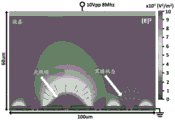
Figure 9 schematically illustrates one embodiment of a self-locking opto-electronic tweezers (SLOT) platform. The platform utilizes an array of annular lateral phototransistors as optical sensors to trigger the DEP force. Coating with high-k dielectric layer (e.g. 30nm Al)2O3) So as to ensure partial voltage leakage in a dark state, thereby realizing the function of single cell self-locking. The optical illumination turns off the locking function and releases the illuminated cells.
Fig. 10 shows the results of numerical simulations showing the electric field distribution and DEP force direction (arrows) at the light illuminated pixels and dark pixels on the SLOT platform. In the dark state, negative DEP forces will lock the cells to the center of the electrode. In the bright state, the locked cells are pushed out of the center of the electrode.
Fig. 11 shows the results of I-V curve measurements showing dark and photocurrent for the ring transistors on the SLOT platform. Three orders of magnitude increase in photocurrent have been observed to achieve operation in conventional cell culture media (-1S/m). The orange reference line represents the conductivity of the cell culture medium. Accordingly, it is 10 times lower than the bright state and 10 times higher than the dark state.
FIG. 12, panels (a) - (d), shows manipulation of 10 μm microparticles on the SLOT platform. Drawing (a): the particles are self-locking throughout the FOV.About 120,000 particles in 1cm2Self-locking on the chip. Drawings (b) and (d): the particles are manipulated individually. Drawing (c): forming a 5 x 3 array of particles.
Figure 13 shows single cell manipulation in conventional cell culture medium (DMEM) on the SLOT platform. And (3) right: a single target cell moves from position 1 to position 6. Left: details of the movement of a single target cell from position 1 to position 2.
Fig. 14 shows a comparison of the effect of different insulating layers on SLOT operation. The partial voltage leakage was calculated for nine different combinations of insulation layer and liquid conductivity. Based on the calculations we conclude that 30nm Al is in terms of achieving both self-locking and release functions2O3Should be superior to the other two insulating layers in a 1S/m highly conductive medium.
Fig. 15, panels (a) - (c), shows the non-circular phototransistor of SLOT. Drawing (a): the manufacturing process is the same as SLOT. However, in one embodiment of a non-circular SLOT, the P-region (blue region) has been designed to be "bean" shaped (e.g., kidney bean shaped) rather than circular. The green areas represent the open areas on the high-k dielectric coating for electrode-liquid contact. Drawing (b): non-circular SLOT was simulated. Drawing (c): the particles migrate stepwise along the circumference (2Mhz, 0.1S/m, 5 Vpp).
DETAILED DESCRIPTIONS
In various embodiments, a self-locking optoelectronic tweezers (SLOT) is provided. The self-locking opto-electronic tweezers (SLOT) platform described herein overcomes the problem of blurred optical patterns for large area single cell and microparticle manipulation. The SLOT platform described herein provides convenient and efficient manipulation of single cells or microparticles over large areas in physiological or other buffers (e.g., such as isotonic buffers commonly used in DEP techniques). SLOT can be used, inter alia, for sorting rare cells or particles, for in vitro fertilization, for tissue engineering, and in various other environments where manipulation of single cells or particles is required.
It is believed that all existing OET platforms require the projection of a beam to form either positive or negative DEP traps. This means that cells and particles cannot be captured without the presence of a light beam. In order to capture cells using a light beam, two criteria need to be met. First, the light intensity needs to be strong enough so that it can create a virtual electrode and trigger enough electric field to capture the cell. Second, a factor that is generally ignored, but critical for large area single cell manipulation, is the sharpness of the projected light pattern. The blurred light pattern, even strong enough to turn on the virtual electrodes, cannot generate a large enough DEP force for cell manipulation because the DEP force scales linearly with the gradient of the electric field strength. A blurred light pattern with a slowly varying intensity profile does not produce a large enough electric field gradient to result in DEP forces sufficient to effectively capture and manipulate cells.
The sharpness (or resolution) of the projected light pattern is determined by the numerical aperture (n.a.) of the optical system. In order to maintain good clarity for efficient OET manipulation, a 10 x objective is typically used in most OET platforms. However, the 10-fold objective lens has only 1-2 mm2Field of view (FOV). It is possible to use convex lenses with lower n.a. to increase the steering area, but this is at the great sacrifice of-1 cm as we are in holographic OET2The manipulation forces described in (Hsu et al (2010) Lab Chip,19(2): 165-172). Therefore, it is believed to be almost impossible to further extend the single cell manipulation area on OET. The trade-off between high optical resolution patterns and large field of view manipulation is a fundamental physical barrier.
The self-locking opto-electronic tweezers described herein provide a new optical manipulation method and platform that can bypass this fundamental obstacle in order to fit in a very large area (perhaps hundreds of cm) depending on the wafer size and the power that can be supplied2) The use of light beams provides high resolution single cell manipulation functionality.
In various embodiments, the SLOT system includes one or more "top" electrodes, a bottom phototransistor, and a fluidic channel or chamber (e.g., a microfluidic channel) therebetween. Fig. 1 schematically illustrates the operating principle of the SLOT platform. First, as shown in fig. 1(a), particles or cells are introduced into a channel or chamber between the top electrode and the phototransistor substrate (e.g., flowed in through a microfluidic channel). The top and bottom electrodes are wired to an external voltage source (e.g., a function generator). Upon application of an AC voltage, Dielectrophoretic (DEP) traps (negative traps and particles locked in the weak field region) will form and lock individual particles or cells (or particle or cell clusters) to their adjacent ring (ring) phototransistor as shown in fig. 1 (b). Optical observations (e.g., fluorescence, dark field, phase contrast, and others) can be made to identify particles or cells of interest. A light beam then illuminates the target phototransistor-controlled electrode to increase the local photocurrent, temporarily deactivating the negative DEP trap, as shown in fig. 1 (c). Finally, the target particles or cells can be released from their locked-in sites and transported away by the fluid stream for downstream collection and analysis, as shown in fig. 1 (d). Alternatively, the target particles or cells may be retained for further examination and/or manipulation.
Computer simulations were used during the design process to verify concepts. The principle of operation of SLOT was simulated using COMSOL, as shown in fig. 2. If an AC voltage is applied, a negative DEP trap is formed at the ring phototransistor. The AC frequency is chosen such that a portion of the applied voltage can leak through the SU-8 insulator at the large electrode area. This is how particles or cells can lock into the ring phototransistor in the dark state. When a light beam strikes a phototransistor that connects the large electrode to the floating island electrode, it turns on the floating electrode to produce a stronger electric field in the island electrode area than the large electrode area covered by the insulator. This repels the locked particles by negative DEP forces.
As described above, the self-locking function in the SLOT can be realized by partial voltage leakage in the background in the dark state. This leakage voltage depends on several parameters including the thickness of the insulating layer, its dielectric constant, the operating AC frequency and the dielectric conductivity. To understand these relationships, a simple block element model was used to calculate the ratio of voltage drops across the liquid layer and the insulating layer under nine different conditions. Under ideal SLOT operating conditions, the insulating layer should allow approximately 50% partial voltage leakage so that a strong enough self-locking force can be provided in the dark state while maintaining a sufficient electric field strength gradient to repel trapped cells in the bright state. FIG. 14 shows 1 μm SU-8, 30nm SiO2And 30nm Al2O3Insulating layer ofCalculation of the leakage voltage drop in the dark state, where each of them is in a medium with a conductivity of 0.01S/m, 0.1S/m and 1S/m. In one extreme case of using a thick dielectric layer in a highly conductive medium (1 μm SU-8+1S/m), there is no self-locking function due to the majority of the voltage drop across the insulating layer. In a less conductive medium (30nm Al)2O3+0.01S/m) the self-locking function in the dark phase is strong but the release function is not allowed in the bright state, since the close to 100% leakage voltage drop in the medium eliminates the space that creates the electric field strength gradient in the bright state required to repel the trapped cells. Therefore, optimization of the insulating layer thickness and material and matching to the operating medium is important for SLOT operation, and high-k dielectrics (e.g., 30nm Al2O3) Particularly well suited for operation in conducting solutions (e.g., physiological buffer solutions).
The composition and thickness of the insulation (dielectric layer) can be precisely controlled during fabrication. For example, high-k dielectrics can be easily and accurately deposited using Atomic Layer Deposition (ALD) processes.
Fig. 3A and 3B illustrate top and side views of certain embodiments of the SLOT platform. The device shown is fabricated on a p-type silicon substrate. The ring-shaped pattern electrode is formed by photolithography. Between the large electrode and the island electrode, n-type ion implantation is performed to produce an npn phototransistor. 100nm gold (Au) on a 10nm titanium (Ti) film was patterned in a p-type region on the substrate for electrical contact. An N-type substrate with p-type ion implantation can also be fabricated to create a pnp phototransistor to control the floating island electrode. The photodetector structure is not limited to phototransistors. Other structures such as photoconductors and metal-semiconductor-metal (MSM) structures may work in principle as well. The final SU-8 patterning is used to form openings in the floating island electrode regions for fluid contact. It is also possible to use materials such as PDMS, silica, Al2O3Silicon nitride or other dielectric material instead of SU-8 for partial electrical isolation. The architecture of another SLOT platform is shown in fig. 9.
A prototype of SLOT has been successfully manufactured and tested. In the proof-of-concept device, we performed experiments using microparticles (10 μm in diameter) and cells suspended in a conventional physiological buffer or in an isotonic buffer with a conductivity of 0.1S/m. In principle, SLOT also works in other aqueous media, where the conductivity varies from DI water to 5S/m, with appropriately designed plant parameters.
Fig. 4 illustrates the self-locking and selective release functions of SLOT.
The unique feature of SLOT is a self-locking function in the dark state. When a group of particles or cells is introduced onto the SLOT platform, they are individually locked in the ring (ring) phototransistor controlled electrode by negative DEP force without beam irradiation. When the beam strikes one or more ring-shaped phototransistors, it turns off DEP traps in those phototransistors to release the trapped particles or cells. Since the particles or cells are self-locking in the dark state, a large number of ring phototransistors and associated electrodes can be over a large area (e.g., spanning tens or even hundreds of cm)2) Are deployed to capture millions of particles or cells without the need for an active beam.
An optical illumination system with a limited field of view (FOV) but high optical resolution can scan the entire wafer to sequentially selectively release captured cells or particles, similar to the stepper concept used in modern lithography. Alternatively, certain areas may be irradiated (e.g., using a mask) to release a number of cells or particles in selected areas of the substrate. Therefore, the operation area of the SLOT is not limited by the FOV of the objective lens used for imaging and the projection of the optical pattern. For comparison, in conventional OET operation, particles in the area where there is no light illumination will be washed away by the fluid flow.
Furthermore, by coupling the illumination system with the detection system, specific cells or particles (e.g., cells or particles having a specific color or morphology, or cells or particles labeled with a specific, e.g., fluorescent label) may be selectively released or selectively retained. In this manner, the SLOT system described herein can be used as an efficient sorter (e.g., cell sorter).
Although SLOT is described above with respect to a ring-shaped (circular) phototransistor, the phototransistor is not necessarily limited to this shape. In various embodiments, non-circular phototransistors are contemplated. Such phototransistors may include, inter alia, other regular polygonal, elliptical, and irregular phototransistors, including but not limited to kidney-shaped phototransistors. With a circular phototransistor configuration, the cell or particle will only experience a symmetric DEP force, which means that the release direction will only depend on the direction of the background flow. A non-circular phototransistor design (see, e.g., kidney shape in fig. 15) can be used to generate an asymmetric electric field, resulting in a directional DEP force. An advantage of the non-circular design is that the system can operate even without an external fluid pumping system. Using individual non-circular phototransistors as building elements, the combination of a large number of electrodes can be very powerful. For example, we have shown that with a well-controlled laser beam, a single particle can migrate along any pre-designed path (straight line, loop, etc.).
The fabrication of the non-circular phototransistor is the same as the ring phototransistor in SLOT. The difference is in the design process where the shape of the p-region will be non-circular while the width of the p-region remains the same.
Example 1
Self-locking photoelectric tweezers for particle manipulation over large areas
This example describes the design and fabrication of a novel self-locking opto-electronic tweezers (SLOT) platform that overcomes the problem of blurred optical patterns for large area single cell and microparticle manipulation. SLOT is implemented by arranging an array of ring-shaped (ring-shaped) phototransistors that can be optically turned on and off. Single cells and particles self-lock into these ring phototransistors in the dark without light illumination. When the light beam strikes the ring electrode, it closes the DEP traps in the electrode to release trapped particles. Since cells and microparticles are self-locking in the dark state, they can span tens or even hundreds of cm2A large number of ring phototransistors are deployed over a large area to capture millions of single cells. Optical illumination with limited field of view (FOV)The system can scan the entire wafer to selectively release the captured cells, similar to the stepper concept used in modern lithography. Thus, the operation area of the SLOT is not limited to the FOV of the objective lens used for imaging and optical pattern projection. Furthermore, SLOT is also a platform based on single crystal silicon phototransistors. It offers the possibility of single cell manipulation in conventional physiological buffers (Hsu et al (2010) Lab Chip,10(2): 165-172).
Device operation and principles
Fig. 1 schematically illustrates the operation of one embodiment of the SLOT platform, an exemplary configuration of which is shown in fig. 3A and 3B. As shown, the SLOT system includes a top surface that includes an electrode, a bottom phototransistor, and a fluidic channel or chamber (e.g., microfluidic channel) therebetween. For example, particles or cells are introduced onto the platform by microfluidic channel inflow.
The top and bottom electrodes (see, e.g., fig. 3B) are electrically connected to a voltage source (e.g., a function generator). Once a voltage (e.g., AC voltage) is applied to an electrode, DEP traps are formed and individual particles (or cells) are locked to their neighboring phototransistor ring electrodes. Next, optical (e.g., fluorescence, dark field, phase contrast, and others) or other observations can be made to identify the particles or cells of interest. The beam then illuminates the target phototransistor which increases the local photoconductivity and temporarily deactivates the corresponding DEP trap. Finally, the targeted single particles or cells (or particle clusters or cell clusters) are released from the locked-in site and transported away, e.g., by continuous flow, for downstream collection and analysis. Alternatively, the target particles or cells (or particle clusters or cell clusters) may be retained for analysis or further processing, and unwanted particles or cells (or particle clusters or cell clusters) may be released.
In some embodiments, the light beam may be directed to individual phototransistor sites to release the portion trapped in a single DEP trap. In certain embodiments, a light beam may be directed to a plurality of phototransistor sites, for example, using a mask, to release portions trapped at a plurality of DEP traps.
Device fabrication and simulation
Fig. 3A and 3B show top and side views of an exemplary SLOT platform. The devices shown are fabricated on a p-type silicon substrate (e.g., on a highly doped p-type substrate). A ring-shaped pattern is formed by photolithography and then used as a mask for n-type ion implantation. 100nm gold (Au) on a 10nm titanium (Ti) thin film was then evaporated onto the substrate followed by SU-8 patterning to form openings for contact with the fluid electrodes. We used COMSOL to simulate the principle of operation of SLOT as shown in fig. 2. If only an AC voltage is applied, a negative DEP trap is formed at the ring electrode. The AC frequency is chosen such that a portion of the applied voltage leaks through the SU-8 insulator at the large electrode area. When a light beam strikes a phototransistor that connects the large electrode with a floating island electrode, it turns on the floating electrode to generate a strong electric field in the island electrode, which repels the trapped particles by negative DEP forces.
It should be recognized that the configuration shown is illustrative and not limiting. It will be appreciated that the device may be configured to have opposite doping, for example, to form a ring-shaped n-p-n phototransistor. Additionally, the dimensions may vary, for example, as described and claimed herein.
In a proof-of-concept device, we performed experiments with microparticles (10 μm in diameter) suspended in an isotonic buffer with a conductivity of 0.1S/m. In fig. 4, we illustrate the self-locking and selective release of single particles on SLOT. SLOT may be scaled up to be able to operate over large areas.
The data presented herein illustrate a novel SLOT platform for self-locking and selective release of single microparticles and single cells (or particle clusters or cell clusters) over large areas. In one exemplary embodiment, SLOT is a single crystal phototransistor-based OET system with the potential for single cell manipulation in conventional physiological buffers. However, SLOT does not necessarily need to be fabricated on monocrystalline silicon. The particle manipulation concept of SLOT can be implemented on amorphous or polycrystalline silicon based ring phototransistor structures. Other semiconductor materials, such as group III-V materials, may also be used.
Exemplary embodiments of the inventionBut not limiting operating parameters of the embodiment
Manufacturing high sensitivity SLOT:
joint width: 2 μm;
ion implantation: 1e15cm-2 200keV,4e15cm-215keV (surface);
annealing: 1000 ℃ for 1 hour
An electrode: au (100nm) on Ti (10nm)
Insulating layer: 2 μm.
Simulating self-locking and release (see, e.g., fig. 5);
automated single cell capture over large areas;
selective single cell release over large areas;
10Vpp (voltage), 10MHz (frequency), 20 μm (device pitch), 1S/m (dielectric conductivity).
Photoelectric property test (see, for example, fig. 6).
The 1000-fold photoconductivity under the DC power supply is increased;
conductivity: an off state (0.005S/m) < < PBS medium (1S/m) < on state (2S/m);
testing for large area self-locking effects (see, e.g., fig. 7).
10Vpp (voltage), 10MHz (frequency), 20 μm (device spacing), 1S/m (dielectric conductivity)
Single cell self-locking and Release in conventional PBS buffer (see, e.g., FIG. 8)
Observed single cell self-locking effect;
observed release of selectively fluorescently labeled single cells;
10Vpp (voltage), 10MHz (frequency), 20 μm (device spacing), 1S/m (dielectric conductivity, PBS).
The foregoing embodiments are intended to be illustrative and not limiting. Those skilled in the art will recognize variations. For example, the size of the annular region comprising the device may depend on the application. To capture cells (or particles) of size-10 μm, a circle as shown herein having a diameter of about 15 μm is suitable. Larger size loops such as eggs will be sufficient to capture larger cells, clusters, other collections of cells. In order to capture smaller particles or bacteria (e.g., about 1-2 μm), a small size of the ring is sufficient. Thus, in certain embodiments, a ring diameter ranging from about 1 μm, or about 2 μm, or about 5 μm, or about 10 μm, or about 15 μm up to about 200 μm, or up to about 150 μm, or up to about 100 μm, or up to about 50 μm, or up to about 40 μm, or up to about 30 μm is contemplated. In certain embodiments, the cyclics range in diameter from about 5 μm to about 50 μm.
The width of the doped rings forming the ring transistor will control the transistor characteristics. In certain embodiments, the annulus thickness ranges from about 0.5 μm up to about 10 μm. A thinner annular ring may provide a higher optical gain, which allows the use of lower light intensity to turn on the electrodes. The trade-off is the small voltage swing at which it can operate because the phototransistor can be turned on at high voltages without light illumination. If a larger width is used, the optical gain can be lower, but on the other hand we can operate the device at a high voltage to create a larger trapping force on the cell.
Example 2
Single cell manipulation in cell culture media over large areas using self-locking optoelectronic tweezers
This example describes a novel self-locking optoelectronic tweezers (SLOT) for single cell manipulation in cell culture media over large areas (see, e.g., fig. 9). SLOT overcomes two major technical obstacles of conventional optoelectronic tweezers (OET) to high-throughput single-cell manipulation. In one exemplary but non-limiting embodiment, the SLOT is fabricated by arranging an array of lateral phototransistor-based ring electrodes that can be optically turned on and off. The lateral ring phototransistor design enables manipulation in high conductivity media (1S/m) and overcomes in large areas (1S/m)>1cm2) The problem of the basic blurred optical pattern of single cell manipulation in (1).
The principle of operation.
DEP traps powered by an external function generator are formed around the ring electrode, where single cells self-lock in the dark state without requiring light illumination. When the ring electrode is illuminated by the light beam, the DEP trap is closed to release the illuminated single cell. This mechanism of operation can easily be scaled to very large areas, even across the entire wafer, to capture millions of single cells in parallel. The operational concept of SLOT is similar to the stepper used in modern microfabrication. The optical illumination system can scan the entire wafer to release the cells of interest while other outside-FOV cells remain self-locked.
Simulation and fabrication
SLOT has two operating states: a dark state and a light state. In the dark state, only an ac voltage is applied. In the bright state, both an ac voltage and an illumination beam are applied. To understand how SLOT works in the dark and light states, it is useful to perform numerical simulations. Fig. 10 shows the numerical simulated electric field intensity distribution and DEP force at the light irradiation pixel and the surrounding dark pixels. Applying a high frequency (10MHz) ac bias to pass Al2O3The insulating layer (30nm) produced partial voltage leakage to form a negative DEP single cell trap in the dark state. DEP force is directed towards the center of the electrode in the dark state, locking the single cell. Conversely, in the bright state, the DEP force is directed towards the center of the electrode, releasing a single cell. This is the fundamental reason that self-locking and selective release can be achieved. The decoupling commitment of the self-locking and light release functions extends the SLOT to very large areas.
In one exemplary embodiment, the device is fabricated on a p-type highly doped single crystal silicon substrate. The annular pattern is created by photolithography and is used as an n-type ion implantation mask. 100nm (Au) on a 10nm (Ti) metal film is evaporated to the substrate, followed by a lift-off process. Finally, we formed 30nm Al2O3A pattern of thin films with an array of 5 μm circular openings for electrode buffer contact. Notably, Al2O3The membrane is chosen because it plays an important role in achieving the self-locking and release functions. The film should be thin and have a high dielectric constant so that an electric field from an ac voltage can pass through a thin film portion in a dark stateThe ground leaks to realize the self-locking function. The biocompatible double-sided adhesive tape was patterned by a commercial paper cutter and used as a microfluidic channel through which a cell sample could be introduced. The channel width is approximately 200 μm. Unlike conventional vertical phototransistor designs, we propose and implement a lateral phototransistor design that requires only one ion implantation and no trench isolation. The doping concentration and thickness of the ion implantation have been optimized. The greatest advantage of the lateral design compared to the vertical design is that DEP capture is no longer dependent on light illumination, so that the capture area can be extended to the entire wafer level. Another benefit of the lateral design is that the photon and electron paths are separated, so we have the freedom to independently adjust the light absorption and device structure.
Features of the apparatus
We further integrated the laser scanning system with the fluorescence microscope to perform calibration of device features and operating conditions. A 532nm 10mW green laser was directed and focused onto the device surface by a set of labview controlled scanning mirrors. The laser power was adjusted using a linear polarizer so that the light intensity was at 0.5W/cm2And 5W/cm2In the meantime.
A circular test structure fabricated with the actual device was used for the electrical characteristics as shown in fig. 11. At 1W/cm2The I-V curve was recorded at illumination intensity. Due to the high phototransistor gain and carrier mobility in single crystal silicon, a photocurrent at 10V peak-to-peak voltage was observed at the bright state three orders of magnitude higher than in the dark state. A reference line (orange) indicating the conductivity of the cell culture medium is also drawn, which shows that the resistance of the phototransistor in the dark state is at least 10 times greater and the resistance of the phototransistor in the bright state is 10 times less compared to the resistance of the cell culture medium.
Results of the experiment
We illustrate SLOT at 1X 1cm2Various manipulation functions on the regions in cell culture medium (DMEM) as shown in fig. 12. Here we show large area self-locking, individual motion and array formation. In fig. 12, panel a, self-locking over a very large area is shown. General description of the inventionThe working area of the device exceeds 1cm2. However, due to the limitations of the FOV of the microscope, we can only observe a relatively small area at a time.
Based on the above discussion, the self-locking function is completely independent of observation, so that the effective self-locking area can extend to even the entire wafer level as long as sufficient electrical power is provided. In fig. 12, panel b and fig. 12, panel d, single cell manipulation is achieved by a projected laser beam. The plurality of particles are released sequentially. In fig. 12, panel c, a 5 × 3 array of microparticles is formed.
At 1cm2Approximately 120,000 particles were captured on the SLOT platform and each of them could be sequentially studied and optically released. One experimental detail that should be noted is that in order to achieve ultra-large area self-locking and release, a separate universal function generator may no longer be suitable, as the power consumed by the device may easily go out of specification, especially in highly conductive cell culture media. Here we use a high power amplifier capable of amplifying a 12MHz ac input.
Single cell manipulation in conventional cell culture media is critical for many real biomedical applications. However, most OET-based technologies can only work in low conductivity media (typically 0.01S/m). Normal cell behavior such as proliferation and growth cannot be expected in media other than normal physiological buffers (usually 1S/m). mu.L of sample solution (Ramos suspended in DMEM) was introduced into the SLOT apparatus with an external function generator set at 8MHz and 10 Vpp. We demonstrate that the beam within the field of view of the objective lens selectively releases a single cell of interest.
In fig. 13, we show how the target cells of interest move sequentially from position 1 to position 6, while the non-target cells remain locked. Initially, both cells were self-locked by DEP traps. We then move the laser beam to the location where the target cell is located. This results in a significant increase in photocurrent at the illuminated phototransistor. Thus, the DEP trap is turned off and the trapped cells are released by the background microfluidic flow. Less than 0.5s is required to release the cells from the trap. A typical background flow rate is 50 μm/s. These parameters vary with different experimental conditions.
The operation of SLOT is similar to the "stepper" concept that is widely used in modern lithography. We project a fixed or programmable light pattern onto the SLOT substrate. The cells of interest may be released individually or in batches. Since the position of each electrode has been pre-designed, the release function can be performed without real-time observation, indicating the ability of the SLOT to manipulate the cell even beyond the field of view of the objective.
Summary of the invention
We report a new self-locking optoelectronic tweezers (SLOT) for single cell manipulation in cell culture medium over large areas. SLOT solves two major technical obstacles of conventional optoelectronic tweezers (OET) for single cell manipulation over large areas in conventional physiological buffers. Has been manipulated in high conductivity media by its unique lateral ring phototransistor design (>1S/m) high throughput (over 120,000 particles) manipulation is achieved. The self-locking concept is to extend the operating area of the conventional OET to 1cm2Or even more critical. Potential applications of SLOT include tissue engineering, drug screening (Nilsson et al (2009) analytical Chimica Acta,649(2): 141-.
It is understood that the examples and embodiments described herein are for illustrative purposes only and that various modifications or changes in light thereof will be suggested to persons skilled in the art and are to be included within the spirit and purview of this application and scope of the appended claims. All publications, patents, and patent applications cited herein are hereby incorporated by reference in their entirety for all purposes.
Claims (58)
1. A self-locking optical tweezers device, comprising:
a first substrate comprising a first electrode and a plurality of ring-shaped and/or non-circular phototransistors that can be optically turned on and off, wherein the phototransistors and first substrate are configured to generate a negative dielectrophoretic force DEP at the ring-shaped or non-circular phototransistors upon application of a voltage to the device; and turning off the DEP at a ring-shaped or non-circular phototransistor when the phototransistor is illuminated with light; and
a surface comprising a second electrode, wherein the surface is arranged to define a chamber or channel between the first substrate and the surface, and the chamber or channel is configured to receive and, or hold, a fluid containing cells or particles.
2. The device of claim 1, wherein the phototransistor is ring-shaped.
3. The apparatus of claim 1, wherein the non-circular phototransistor is bean-shaped.
4. The apparatus of claim 1, wherein the phototransistor generates an electric field perpendicular to a plane of the device.
5. The apparatus of claim 2, wherein the phototransistor generates an electric field perpendicular to a plane of the device.
6. The apparatus of claim 3, wherein the phototransistor generates an electric field perpendicular to a plane of the device.
7. The device of any of claims 1-6, wherein the annular or non-circular portion of the phototransistor is p-doped.
8. The device of any one of claims 1-6, wherein the substrate is a doped p-type substrate comprising a ring-shaped or bean-shaped portion, wherein a center of the ring-shaped or bean-shaped portion and a region outside the ring-shaped or non-circular portion are n-doped.
9. The device of claim 8, wherein the doped p-type substrate is a doped p-type group III-V or p-type group IV material.
10. The device of claim 8, wherein the doped p-type substrate is doped p-type silicon.
11. The device of claim 8, wherein the n-doped region is coated with a thin film conductor.
12. The apparatus of claim 11, wherein one or more of the thin film conductors comprises a material selected from the group consisting of Au, Ti, Al, Cr, Ni, Ta, Pd, and Pt.
13. The apparatus of claim 11, wherein a top surface of the substrate is coated with an insulator having an opening to the thin film conductor at a center of the annular or non-circular shape.
14. The apparatus of claim 13, wherein the insulator comprises a material selected from the group consisting of SU-8 or other photoresist, PDMS, silicon dioxide, Al2O3And silicon nitride.
15. The apparatus of claim 13, wherein the insulator is configured to provide 50% partial voltage leakage in the dark state.
16. The apparatus of claim 13, wherein the insulator comprises Al2O3。
17. The device of any of claims 1-6, wherein the annular or non-circular portion of the phototransistor is n-doped.
18. The device of any of claims 1-6, wherein the substrate is a doped n-type substrate comprising a ring-shaped or non-circular portion, wherein a center of the ring-shaped or non-circular portion and a region outside the ring-shaped or non-circular portion are p-doped.
19. The device of claim 18, wherein the doped n-type substrate is a doped n-type group III-V or n-type group IV material.
20. The device of claim 18, wherein the doped n-type substrate is doped n-type silicon.
21. The device of claim 18, wherein the p-doped region is coated with a thin film conductor.
22. The apparatus of claim 21, wherein one or more of the thin film conductors comprises a material selected from the group consisting of Au, Ti, Al, Cr, Ni, Ta, Pd, and Pt.
23. The apparatus of claim 21, wherein a top surface of the substrate is coated with an insulator having an opening to the thin film conductor at a center of the annular or non-circular shape.
24. The apparatus of claim 23, wherein the insulator comprises a material selected from the group consisting of SU-8 or other photoresist, PDMS, silicon dioxide, Al2O3And silicon nitride.
25. The device of claim 23, wherein the insulator is configured to provide 50% partial voltage leakage in the dark state.
26. The apparatus of claim 23, wherein the insulator comprises Al2O3。
27. The device of claim 26, wherein Al2O3Is 30 nm.
28. The device of any of claims 1-6, wherein the liner isThe size of the bottom ranges from 1mm2Or 5mm2Or 10mm2Or 50mm2Or 1cm2Up to 500cm2Or up to 200cm2Or up to 100cm2Or up to 50cm2。
29. The device of any one of claims 1-6, wherein the diameter of the annulus or the long axis of the non-circular shape ranges from 10, or 20nm, or 50nm, or 100nm, or 200nm, or 500nm up to 500 μ ι η, or up to 250 μ ι η, or up to 200 μ ι η, or up to 100 μ ι η, or up to 150 μ ι η, or up to 80 μ ι η, or up to 60 μ ι η, or up to 50 μ ι η, or up to 30 μ ι η, or up to 20 μ ι η.
30. The device of claim 29, wherein the diameter of a ring or the major axis of a non-circular shape is 10 μ ι η to 20 μ ι η.
31. The device of claim 29, wherein the diameter of a ring or the major axis of a non-circular shape is 15 μ ι η.
32. The device of any one of claims 1-6, wherein the thickness of the rings forming the annulus or non-circular shape is in the range of 0.5 μm up to 10 μm.
33. The device of claim 26, wherein the thickness of the rings forming the annulus or non-circular shape is in the range of 2 μ ι η up to 8 μ ι η.
34. The device of claim 27, wherein the thickness of the rings forming the annulus or non-circular shape is 5 μ ι η.
35. The device of any one of claims 1-6, wherein the chamber or channel contains a physiological buffer.
36. The device of any one of claims 1-6, wherein the chamber or channel contains an isotonic buffer.
37. The device of any one of claims 1-6, wherein the chamber or channel contains particles.
38. The device of any one of claims 1-6, wherein the chamber or channel contains cells.
39. The device of any one of claims 1-6, wherein the chamber or channel contains prokaryotic cells.
40. The device of claim 39, wherein the chamber or channel contains bacterial cells.
41. The device of any one of claims 1-6, wherein the chamber or channel contains eukaryotic cells.
42. The device of claim 41, wherein the chamber or channel contains insect cells, mammalian cells, or avian cells.
43. The device of any one of claims 1-6, wherein the chamber or channel contains an egg or embryo.
44. A method of capturing cells or particles, the method comprising:
introducing cells or particles into a chamber of a device according to any one of claims 1-33; and
applying a voltage between the first electrode and the second electrode to capture the cells or particles at a ring transistor comprising the substrate.
45. The method of claim 44, further comprising illuminating one or more phototransistors to release the captured particles or cells.
46. The method of claim 44 or 45, wherein the voltage is an AC voltage.
47. The method of claim 46, wherein the voltage range is 0.5V to 100V pp.
48. The method of claim 46, wherein the voltage has a frequency in the range of 1kHz to 50 MHz.
49. The method of claim 47, wherein the voltage has a frequency in the range of 1kHz to 50 MHz.
50. The method of claim 44 or 45, wherein the chamber or channel contains a physiological buffer.
51. The method of claim 44 or 45, wherein the chamber or channel contains an isotonic buffer.
52. The method of claim 44 or 45, wherein the chamber or channel contains a particle or cluster of particles.
53. The method of claim 44 or 45, wherein the chamber or channel contains a cell or cluster of cells.
54. The method of claim 53, wherein the chamber or channel contains a prokaryotic cell.
55. The method of claim 54, wherein the chamber or channel contains bacterial cells.
56. The method of claim 53, wherein the chamber or channel contains eukaryotic cells.
57. The method of claim 56, wherein the chamber or channel contains insect cells, mammalian cells, or avian cells.
58. The method of claim 44 or 45, wherein the chamber or channel contains an egg or embryo.
Applications Claiming Priority (5)
| Application Number | Priority Date | Filing Date | Title |
|---|---|---|---|
| US201462038150P | 2014-08-15 | 2014-08-15 | |
| US62/038,150 | 2014-08-15 | ||
| US201562181627P | 2015-06-18 | 2015-06-18 | |
| US62/181,627 | 2015-06-18 | ||
| PCT/US2015/045387 WO2016025901A1 (en) | 2014-08-15 | 2015-08-14 | Self-locking optoelectronic tweezer and its fabrication |
Publications (2)
| Publication Number | Publication Date |
|---|---|
| CN107250344A CN107250344A (en) | 2017-10-13 |
| CN107250344B true CN107250344B (en) | 2021-01-12 |
Family
ID=55304689
Family Applications (1)
| Application Number | Title | Priority Date | Filing Date |
|---|---|---|---|
| CN201580055791.0A Active CN107250344B (en) | 2014-08-15 | 2015-08-14 | Self-locking photoelectric tweezers and manufacture thereof |
Country Status (9)
| Country | Link |
|---|---|
| US (2) | US10465154B2 (en) |
| EP (1) | EP3180418A4 (en) |
| JP (1) | JP6925967B2 (en) |
| KR (1) | KR102425337B1 (en) |
| CN (1) | CN107250344B (en) |
| AU (1) | AU2015301481A1 (en) |
| CA (1) | CA2957780A1 (en) |
| IL (1) | IL250630A0 (en) |
| WO (1) | WO2016025901A1 (en) |
Families Citing this family (6)
| Publication number | Priority date | Publication date | Assignee | Title |
|---|---|---|---|---|
| EP3180418A4 (en) | 2014-08-15 | 2018-04-18 | The Regents of The University of California | Self-locking optoelectronic tweezer and its fabrication |
| US10953408B2 (en) * | 2018-09-04 | 2021-03-23 | The Governing Council Of The University Of Toronto Banting Institute | Patterned optoelectronic tweezers |
| CN113348036A (en) * | 2018-11-19 | 2021-09-03 | 伯克利之光生命科技公司 | Microfluidic device with programmable switching elements |
| CN109810894B (en) * | 2019-03-01 | 2022-06-10 | 长春理工大学 | Group cell three-dimensional structure manipulation and construction system and method based on light-induced dielectrophoresis |
| CN112461803B (en) * | 2020-06-12 | 2023-07-07 | 重庆工商大学 | Method for detecting aflatoxin B1 and ochratoxin A in food sample |
| TWI803169B (en) * | 2022-01-25 | 2023-05-21 | 友達光電股份有限公司 | Optoelectronic tweezer device and fabrication method thereof |
Family Cites Families (7)
| Publication number | Priority date | Publication date | Assignee | Title |
|---|---|---|---|---|
| WO2005100541A2 (en) | 2004-04-12 | 2005-10-27 | The Regents Of The University Of California | Optoelectronic tweezers for microparticle and cell manipulation |
| GB0410579D0 (en) | 2004-05-12 | 2004-06-16 | Univ St Andrews | Optoelectronic tweezers |
| WO2008088395A2 (en) * | 2006-08-31 | 2008-07-24 | Massachusetts Institute Ot Technology | Optofluidic-based particle sorting |
| WO2008119066A1 (en) | 2007-03-28 | 2008-10-02 | The Regents Of The University Of California | Single-sided lateral-field and phototransistor-based optoelectronic tweezers |
| US20140216935A1 (en) * | 2012-08-08 | 2014-08-07 | Lehigh University | Dielectrophoretic Tweezers as a Platform for Molecular Force Spectroscopy in a Highly Parallel Format |
| US9403172B2 (en) * | 2012-11-08 | 2016-08-02 | Berkeley Lights, Inc. | Circuit based optoelectronic tweezers |
| EP3180418A4 (en) | 2014-08-15 | 2018-04-18 | The Regents of The University of California | Self-locking optoelectronic tweezer and its fabrication |
-
2015
- 2015-08-14 EP EP15831613.3A patent/EP3180418A4/en not_active Withdrawn
- 2015-08-14 CN CN201580055791.0A patent/CN107250344B/en active Active
- 2015-08-14 KR KR1020177007049A patent/KR102425337B1/en active IP Right Grant
- 2015-08-14 WO PCT/US2015/045387 patent/WO2016025901A1/en active Application Filing
- 2015-08-14 CA CA2957780A patent/CA2957780A1/en not_active Abandoned
- 2015-08-14 US US15/501,428 patent/US10465154B2/en active Active
- 2015-08-14 JP JP2017508505A patent/JP6925967B2/en active Active
- 2015-08-14 AU AU2015301481A patent/AU2015301481A1/en not_active Abandoned
-
2017
- 2017-02-15 IL IL250630A patent/IL250630A0/en unknown
-
2019
- 2019-10-29 US US16/667,801 patent/US11162060B2/en active Active
Non-Patent Citations (1)
| Title |
|---|
| Phototransistor-based optoelectronic tweezers for dynamic cell manipulation in cell culture media;Hsan-yin Hsu et al;《Lab on a Chip》;20101231(第10期);165-172 * |
Also Published As
| Publication number | Publication date |
|---|---|
| US20170226453A1 (en) | 2017-08-10 |
| US20200140798A1 (en) | 2020-05-07 |
| AU2015301481A1 (en) | 2017-03-02 |
| IL250630A0 (en) | 2017-04-30 |
| KR102425337B1 (en) | 2022-07-25 |
| CA2957780A1 (en) | 2016-02-18 |
| EP3180418A1 (en) | 2017-06-21 |
| JP6925967B2 (en) | 2021-08-25 |
| EP3180418A4 (en) | 2018-04-18 |
| CN107250344A (en) | 2017-10-13 |
| JP2017525358A (en) | 2017-09-07 |
| WO2016025901A1 (en) | 2016-02-18 |
| US11162060B2 (en) | 2021-11-02 |
| KR20170041911A (en) | 2017-04-17 |
| US10465154B2 (en) | 2019-11-05 |
Similar Documents
| Publication | Publication Date | Title |
|---|---|---|
| CN107250344B (en) | Self-locking photoelectric tweezers and manufacture thereof | |
| Hsu et al. | Phototransistor-based optoelectronic tweezers for dynamic cell manipulation in cell culture media | |
| US7956339B2 (en) | Single-sided lateral-field and phototransistor-based optoelectronic tweezers | |
| JP5349044B2 (en) | Method and apparatus for particle manipulation and / or detection | |
| JP2007537729A (en) | Optoelectronic tweezers for manipulation of microparticles and cells | |
| US20060175192A1 (en) | Optoelectronic probe | |
| Zhang et al. | Optoelectronic tweezers: a versatile toolbox for nano-/micro-manipulation | |
| US10953408B2 (en) | Patterned optoelectronic tweezers | |
| Huang et al. | Optoelectronic tweezers integrated with lensfree holographic microscopy for wide-field interactive cell and particle manipulation on a chip | |
| Mishra et al. | Optoelectrical microfluidics as a promising tool in biology | |
| Yang et al. | Cell patterning via diffraction-induced optoelectronic dielectrophoresis force on an organic photoconductive chip | |
| Humbert et al. | Versatile, rapid and robust nano-positioning of single-photon emitters by AFM-nanoxerography | |
| Hoshino et al. | Electron beam induced fine virtual electrode for mechanical strain microscopy of living cell | |
| Yang et al. | Single cell manipulation in cell culture media with Self-Locking Optoelectronic Tweezers across a large area | |
| Cheng et al. | Single CdSe Quantum Dots Positioned in Nanostructured Heterogeneous Templates: Implications for High-Precision Nanoassembly | |
| JP2009002745A (en) | Light induced dielectric migration apparatus | |
| Ohta et al. | Optoelectronic tweezers for the manipulation of cells, microparticles, and nanoparticles | |
| Chuang et al. | Optoelectrokinetic Manipulation for Cell Analysis | |
| Higuchi et al. | Manipulation system for nano/micro components integration via transportation and self-assembly | |
| Lu | Confocal scanning optical microscopy and nanotechnology | |
| US20120061241A1 (en) | Apparatus and associated methods | |
| Chiou | Massively parallel optical manipulation of single cells, micro-and nano-particles on optoelectronic devices | |
| Heng et al. | Optofluidic microscopy | |
| Qu et al. | Fully automatic wafer-scale micro/nano manipulation based on optically induced dielectrophoresis | |
| Li et al. | DNA Network Construction by Optically Induced Dielectrophoresis |
Legal Events
| Date | Code | Title | Description |
|---|---|---|---|
| PB01 | Publication | ||
| PB01 | Publication | ||
| SE01 | Entry into force of request for substantive examination | ||
| SE01 | Entry into force of request for substantive examination | ||
| GR01 | Patent grant | ||
| GR01 | Patent grant |