CN107209735B - Configurable die, package on package device and method - Google Patents
Configurable die, package on package device and method Download PDFInfo
- Publication number
- CN107209735B CN107209735B CN201680005707.9A CN201680005707A CN107209735B CN 107209735 B CN107209735 B CN 107209735B CN 201680005707 A CN201680005707 A CN 201680005707A CN 107209735 B CN107209735 B CN 107209735B
- Authority
- CN
- China
- Prior art keywords
- phy
- memory
- generic
- signal
- signals
- Prior art date
- Legal status (The legal status is an assumption and is not a legal conclusion. Google has not performed a legal analysis and makes no representation as to the accuracy of the status listed.)
- Active
Links
Images


Classifications
-
- G—PHYSICS
- G11—INFORMATION STORAGE
- G11C—STATIC STORES
- G11C7/00—Arrangements for writing information into, or reading information out from, a digital store
- G11C7/22—Read-write [R-W] timing or clocking circuits; Read-write [R-W] control signal generators or management
-
- G—PHYSICS
- G06—COMPUTING; CALCULATING OR COUNTING
- G06F—ELECTRIC DIGITAL DATA PROCESSING
- G06F13/00—Interconnection of, or transfer of information or other signals between, memories, input/output devices or central processing units
- G06F13/14—Handling requests for interconnection or transfer
- G06F13/16—Handling requests for interconnection or transfer for access to memory bus
- G06F13/1668—Details of memory controller
- G06F13/1694—Configuration of memory controller to different memory types
-
- G—PHYSICS
- G11—INFORMATION STORAGE
- G11C—STATIC STORES
- G11C7/00—Arrangements for writing information into, or reading information out from, a digital store
- G11C7/10—Input/output [I/O] data interface arrangements, e.g. I/O data control circuits, I/O data buffers
-
- G—PHYSICS
- G11—INFORMATION STORAGE
- G11C—STATIC STORES
- G11C8/00—Arrangements for selecting an address in a digital store
- G11C8/06—Address interface arrangements, e.g. address buffers
-
- G—PHYSICS
- G11—INFORMATION STORAGE
- G11C—STATIC STORES
- G11C8/00—Arrangements for selecting an address in a digital store
- G11C8/18—Address timing or clocking circuits; Address control signal generation or management, e.g. for row address strobe [RAS] or column address strobe [CAS] signals
-
- H—ELECTRICITY
- H01—ELECTRIC ELEMENTS
- H01L—SEMICONDUCTOR DEVICES NOT COVERED BY CLASS H10
- H01L2224/00—Indexing scheme for arrangements for connecting or disconnecting semiconductor or solid-state bodies and methods related thereto as covered by H01L24/00
- H01L2224/01—Means for bonding being attached to, or being formed on, the surface to be connected, e.g. chip-to-package, die-attach, "first-level" interconnects; Manufacturing methods related thereto
- H01L2224/10—Bump connectors; Manufacturing methods related thereto
- H01L2224/15—Structure, shape, material or disposition of the bump connectors after the connecting process
- H01L2224/16—Structure, shape, material or disposition of the bump connectors after the connecting process of an individual bump connector
- H01L2224/161—Disposition
- H01L2224/16151—Disposition the bump connector connecting between a semiconductor or solid-state body and an item not being a semiconductor or solid-state body, e.g. chip-to-substrate, chip-to-passive
- H01L2224/16221—Disposition the bump connector connecting between a semiconductor or solid-state body and an item not being a semiconductor or solid-state body, e.g. chip-to-substrate, chip-to-passive the body and the item being stacked
- H01L2224/16225—Disposition the bump connector connecting between a semiconductor or solid-state body and an item not being a semiconductor or solid-state body, e.g. chip-to-substrate, chip-to-passive the body and the item being stacked the item being non-metallic, e.g. insulating substrate with or without metallisation
-
- H—ELECTRICITY
- H01—ELECTRIC ELEMENTS
- H01L—SEMICONDUCTOR DEVICES NOT COVERED BY CLASS H10
- H01L2224/00—Indexing scheme for arrangements for connecting or disconnecting semiconductor or solid-state bodies and methods related thereto as covered by H01L24/00
- H01L2224/01—Means for bonding being attached to, or being formed on, the surface to be connected, e.g. chip-to-package, die-attach, "first-level" interconnects; Manufacturing methods related thereto
- H01L2224/42—Wire connectors; Manufacturing methods related thereto
- H01L2224/47—Structure, shape, material or disposition of the wire connectors after the connecting process
- H01L2224/48—Structure, shape, material or disposition of the wire connectors after the connecting process of an individual wire connector
- H01L2224/4805—Shape
- H01L2224/4809—Loop shape
- H01L2224/48091—Arched
-
- H—ELECTRICITY
- H01—ELECTRIC ELEMENTS
- H01L—SEMICONDUCTOR DEVICES NOT COVERED BY CLASS H10
- H01L2224/00—Indexing scheme for arrangements for connecting or disconnecting semiconductor or solid-state bodies and methods related thereto as covered by H01L24/00
- H01L2224/01—Means for bonding being attached to, or being formed on, the surface to be connected, e.g. chip-to-package, die-attach, "first-level" interconnects; Manufacturing methods related thereto
- H01L2224/42—Wire connectors; Manufacturing methods related thereto
- H01L2224/47—Structure, shape, material or disposition of the wire connectors after the connecting process
- H01L2224/48—Structure, shape, material or disposition of the wire connectors after the connecting process of an individual wire connector
- H01L2224/481—Disposition
- H01L2224/48151—Connecting between a semiconductor or solid-state body and an item not being a semiconductor or solid-state body, e.g. chip-to-substrate, chip-to-passive
- H01L2224/48221—Connecting between a semiconductor or solid-state body and an item not being a semiconductor or solid-state body, e.g. chip-to-substrate, chip-to-passive the body and the item being stacked
- H01L2224/48225—Connecting between a semiconductor or solid-state body and an item not being a semiconductor or solid-state body, e.g. chip-to-substrate, chip-to-passive the body and the item being stacked the item being non-metallic, e.g. insulating substrate with or without metallisation
- H01L2224/48227—Connecting between a semiconductor or solid-state body and an item not being a semiconductor or solid-state body, e.g. chip-to-substrate, chip-to-passive the body and the item being stacked the item being non-metallic, e.g. insulating substrate with or without metallisation connecting the wire to a bond pad of the item
-
- H—ELECTRICITY
- H01—ELECTRIC ELEMENTS
- H01L—SEMICONDUCTOR DEVICES NOT COVERED BY CLASS H10
- H01L2924/00—Indexing scheme for arrangements or methods for connecting or disconnecting semiconductor or solid-state bodies as covered by H01L24/00
- H01L2924/15—Details of package parts other than the semiconductor or other solid state devices to be connected
- H01L2924/151—Die mounting substrate
- H01L2924/153—Connection portion
- H01L2924/1531—Connection portion the connection portion being formed only on the surface of the substrate opposite to the die mounting surface
- H01L2924/15311—Connection portion the connection portion being formed only on the surface of the substrate opposite to the die mounting surface being a ball array, e.g. BGA
Abstract
A configurable die, comprising: logic elements configured to communicate Control and Address (CA) signals and Data (DQ) signals; and a first universal physical interface (PHY) and a second universal PHY in communication with the logic element, wherein each of the first universal PHY and the second universal PHY may be configured as a CA PHY and a DQ PHY, and wherein the logic element may be configured to communicate CA signals and DQ signals to different ones of the first universal PHY and the second universal PHY.
Description
Technical Field
The present application relates to chip connections to memory devices, and more particularly to chip connections on a common die for accommodating connection of the die to different external memory types with simple packaging and low cost.
Background
Synchronous Dynamic Random Access Memory (SDRAM) is a type of memory used in mobile communication and computing devices, such as smart phones and tablet computers. In some embodiments, double data rate SDRAM (DDR SDRAM or DDR) refers to a type of memory and associated interface for communicating with such memory. Furthermore, low power DDR (LPDDR or LP for short, sometimes referred to as mobile DDR) is a class of DDR designed to reduce power consumption, with mobile devices being the target application. There are several versions of LPDDR that correspond to various data speed and power requirements. For example, LPDDR3 (also sometimes designated LP3) and LPDDR4 (also sometimes designated LP4) are two recent versions of LPDDR. LPDDR4 are designed to communicate at higher speeds and with less power consumption than LPDDR3 at the expense of increased cost and/or complexity.
The trend in modern mobile devices, such as smart phones, is to focus memory design on larger and larger memory transfer rates while saving power. Systems on chip (SoC) are often used in mobile devices to save power and/or minimize space requirements. SoC refers to multiple functional blocks (such as modems and application processor cores) embedded on a single substrate, allowing mobile devices to execute complex and power intensive applications. The single substrate is sometimes referred to as a die, whereby multiple functional blocks are typically implemented collectively on a single die.
In some instances, package on package (PoP) may refer to a package configuration in which two or more packages are stacked on top of each other and interface to pass signals between them. Joint Electron Device Engineering Council (JEDEC) has standardized one or more PoP layouts (football prints) for interfacing with LPDDR3 SDRAM memories. There is at least one proposal in JEDEC for a PoP layout for interfacing with LPDDR4 SDRAM memory. The differences between LPDDR3 and LPDDR4 result in significant differences in the respective layouts.
Mobile device applications require more and faster memory, so for faster memories (such as LPDDR4), the trend is to focus SoC designs and corresponding die designs on optimizing routing and packaging. However, in price sensitive markets (such as markets that focus on low or mid-end smartphones), it may be desirable to provide flexibility to the vendor to trade off price and performance to provision mobile devices at different price points. One option may be to provide LPDDR3 (instead of LPDDR4) as a low cost memory replacement. However, once the SoC die is optimized for LPDDR4 packaging, improving wiring and packaging for LPDDR3 may be prohibitively expensive. Thus, there is a need for SoC dies that flexibly accommodate different memory architectures.
Disclosure of Invention
Dies for supporting different memory types with minimal package complexity are disclosed. In one embodiment, a die common to different memory types may be configured to support each of the two memory types in a PoP configuration with simple interconnections between packages, regardless of which of the two memory types is used. For example, one memory type supported is LPDDR3, while a second memory type supported is LPDDR 4.
In one embodiment, a configurable die is disclosed, comprising: logic elements configured to communicate Control and Address (CA) signals and Data (DQ) signals; and a first universal physical interface (PHY) and a second universal PHY in communication with the logic element. Each of the first and second generic PHYs may be configured as a CA PHY and a DQPHY, and the logic element may be configured to communicate the CA signal and the DQ signal to a different one of the first and second generic PHYs.
In another embodiment, an apparatus is disclosed, comprising: a SoC to selectively support a first type of memory and a second type of memory, the SoC including a generic PHY configurable as a CA PHY and a DQ PHY in response to an input corresponding to a supported one of the first type of memory or the second type of memory. The apparatus also includes means for communicating a CA signal and a DQ signal to the generic PHY in response to the input.
In yet another embodiment, a PoP apparatus is disclosed, which includes: a first package including memory circuitry configured to selectively support one of a first type of memory and a second type of memory. The memory circuitry includes a plurality of PHYs, each of which may be configured as a CA PHY and a DQ PHY. The memory circuitry also includes logic elements configured to communicate CA signals to ones of the plurality of PHYs configured as CA PHYs and to communicate DQ signals to and from ones of the plurality of PHYs configured as DQ PHYs. The PoP apparatus also includes a second package that includes either the first type of memory or the second type of memory. The second package is coupled to the first package in a PoP configuration.
In yet another embodiment, a method for supporting different memory types using a single die is disclosed. The method includes receiving a memory type indication and communicating a CA signal to a first generic PHY based on the memory type indication. The method also includes communicating a DQ signal to a second general purpose PHY based on the memory type indication.
Drawings
Fig. 1 is an architecture diagram illustrating an example SoC die and corresponding architecture according to an embodiment of the present disclosure.
FIG. 2 illustrates an LPDDR3 PoP layout according to an embodiment of the disclosure.
FIG. 3 illustrates an LPDDR4PoP layout according to an embodiment of the disclosure.
FIG. 4 illustrates an LPDDR4 optimized routing between a die and an LPDDR3 PoP layout in accordance with an embodiment of the disclosure.
FIG. 5 illustrates a die that is common to both LPDDR3 and LPDDR4 in accordance with an embodiment of the disclosure.
Fig. 6 illustrates DDR signal logic in accordance with an embodiment of the present disclosure.
Fig. 7 illustrates a portion of DDR signal logic in accordance with an embodiment of the present disclosure.
FIG. 8A illustrates the connection between a shared die configured for LPDDR3 PoP and LPDDR3 layout, and FIG. 8B illustrates the connection between a shared die configured for LPDDR4PoP and LPDDR4 layout, according to an embodiment of the disclosure.
Fig. 9 is an isometric view of a PoP with a common die according to an embodiment of the disclosure.
FIG. 10 illustrates a die including a single clock controller that is common to both LPDDR3 and LPDDR4 in accordance with an embodiment of the disclosure.
Fig. 11 is a flow diagram of an example method of using a common die in accordance with an embodiment of the present disclosure.
Detailed Description
Embodiments of a configurable die that supports multiple types of memory using a relatively simple and low cost PoP configuration are disclosed herein. In one application, the configurable die provides smart phone vendors and manufacturers with the option of using a less expensive memory type for low-end to mid-end smart phones or a more expensive memory type that is faster and/or has a larger capacity than the less expensive memory for high-end smart phones. The same die can be used for both memory types without introducing additional layers for package routing, or other more expensive techniques (such as interposers), regardless of the memory type. Furthermore, no changes to the memory die or memory package are required. By way of example, the types of memory supported by the configurable die include LPDDR3 memory and LPDDR4 memory.
The configurable die may employ several features that enable this flexibility. Example embodiments may include one or more of the following features. First, a generic PHY may be employed that may be configured as a CA PHY or a DQ PHY and may be configured according to the PoP memory layout supported by the die. Second, flexible signal logic elements may be employed for routing CA and DQ signals to and from the appropriate PHY according to the PoP memory layout supported by the die. Third, a clock controller may be employed that provides a matching clock signal to all PHYs on the die to provide any PHY with the flexibility to handle different types of signals according to the PoP memory layout supported by the die. The memory controller is able to generate CA codes with appropriate timing relationships for the different types of memory supported.
Fig. 1 is an architectural diagram illustrating an example system on a chip (SoC)100 die and corresponding architecture. In an embodiment, SoC die 100 is used in a smartphone, tablet computer, or other mobile wireless device. SoC die 100 includes several functional blocks including a multicore processor 110 (sometimes referred to as a central processing unit or CPU), a graphics processor 120, a modem 130, and memory circuitry 140, as shown in fig. 1. Fig. 1 is a logical layout of an SoC die 100 showing each region 110 and 140 corresponding to the mentioned functions as separate and distinct regions, but the actual physical layout may be more complex (e.g., where circuitry of one functional block is interspersed between circuitry of another functional block). In an embodiment, the modem implements baseband processing for any of several known wireless technologies or standards, such as Long Term Evolution (LTE). Processor 110 and 130 refer to areas of SoC die 100 dedicated to those functional blocks. In each of these areas, there is circuitry for the specified function. Memory circuitry 140 may refer to an area of SoC die 100 dedicated to a memory controller and interface circuitry for interfacing to external memory. The external memory may be housed, for example, in a package having an interface for connecting to memory circuitry 140. The memory circuitry 140 may be configured to interface with any type of memory, such as DDR SDRAM, DRAM, or flash memory. For illustration purposes, the present disclosure is directed to DDR SDRAMs, such as LPDDR3 and LPDDR 4. At least one of the multicore processor 110, graphics processor 120, and modem 130 is in communication with memory circuitry 140. The various components may communicate via any form of known connection, such as a bus.
In some embodiments, a "PoP layout" (or simply "layout") refers to the location of electrical connections on a DDR SDRAM memory package. In one embodiment, the PoP layout specifies the locations on the DDR SDRAM memory package to connect to the corresponding SoC package (which includes SoC die 100). Memory circuitry 140 may be designed to accommodate various DDR layouts, such as layouts for LPDDR3 or LPDDR 4. The differences in LPDDR3 and LPDDR4 result in the corresponding layouts being physically different. FIG. 2 illustrates an example LPDDR3 PoP layout 200, and FIG. 3 illustrates an example LPDDR4PoP layout 300. The label x-DQ indicates channel x (0 or 1) for data, and y-CA indicates channel y (0 or 1) for command and address information. The blocks labeled "CA" and "DQ" are fixed DDR physical layer circuits (PHYs) corresponding to CA and DQ signals. The CA and DQ signals for various forms of DDR memory are well known to those of ordinary skill in the art.
Each layout in fig. 2 and 3 illustrates an example 64-bit memory interface. Each layout in fig. 2 and 3 corresponds to various JEDEC proposals or standards. Referring to FIG. 2, in an embodiment, each DQ PHY in the LPDDR3 PoP layout 200 refers to a particular byte (or 8 bits). There are eight DQ bytes, resulting in a 64-bit memory interface (originally two 32-bit channels for LPDDR 3). Similarly for LPDDR4, in an embodiment, each DQ PHY in LPDDR4PoP layout 300 refers to a particular byte, resulting in a 64-bit memory interface (originally four 16-bit channels for LPDDR 4). Each CA interface per channel for LPDDR3 corresponds to 10 bits, while the CA interface per channel for LPDDR4 is 6 bits. In one embodiment, the generic CA PHY supports 6 bits. Generally, in the case of LPDDR4, one CA interface is needed per 16 bits of DQ, whereas in LPDDR3, one CA interface is capable of handling 32 bits of DQ. Thus, two CA PHYs per 32-bit channel are used for both LPDDR3 and LPDDR 4. In an embodiment, the LPDDR4PoP layout is originally 4x16, but the layout is implemented as 2x32 on the die (see two x16 as a single x 32).
As previously discussed, it is desirable in some low-end to mid-end smartphone applications to provide vendors with the flexibility to select between LPDDR3 and LPDDR4 depending on, for example, a desired price point and feature set. One result is that potentially longer interleaving lines would be needed if the die were optimized for LPDDR4PoP and were expected to also cooperate with LPDDR3 PoP, as illustrated in fig. 4. FIG. 4 illustrates the interconnections between the LPDDR4PoP optimized die 410 and the LPDDR3 PoP layout to illustrate the challenges facing signal routing. An interposer or other additional layers (such as layers added to the base package) may be used to manage routing, which may increase undesirable costs and signal integrity risks. In some embodiments, PHY refers to an area on a die that contains circuitry, including clock recovery and input/output (I/O) pads, that provides an interface between the die and DDR SDRAM memory. In an embodiment, LPDDR4 die 410 corresponds to SoC die 100 and specifically indicates a layout of a portion of memory circuitry 140.
FIG. 5 illustrates an embodiment of a die 500 that is common to both LPDDR3 and LPDDR 4. The shared die 500 overcomes many of the problems discussed above. The common die 500 includes a memory controller 510, DDR signal logic 520, and DDR PHYA 531 to L542, as shown in fig. 5. In some embodiments, memory controller 510 is a Bus Integrated Memory Controller (BIMC). One or more of PHYs a 531-L542 are generic or common PHYs that may be configured as CA PHYs or DQ PHYs depending on whether LPDDR3 or LPDDR4 is used. The DQ PHY is bidirectional in the sense that the DQ PHY provides data to be both written to and read from memory. On the other hand, the CA PHY is typically unidirectional to send control and address information to the memory, but normally receives nothing from the memory via the CA PHY. One tradeoff with using common die 500 is that any PHY that is a generic PHY that may be configured as a DQ PHY or a CA PHY may be slightly larger in area than a PHY specifically designed as a DQ PHY or a CA PHY. In addition to providing the benefit of flexibility in being able to select either LPDDR3 or LPDDR4, the slightly larger area of a generic PHY also provides the benefit of reduced routing cost and complexity for die common to both LPDDR3 and LPDDR 4.
Fig. 6 illustrates an embodiment of DDR signal logic 520. DDR signal logic 520 input and output are illustrated. One function of the DDR signal logic 520 is to route signals between the memory controller 510 and the DDR SDRAM. DDR signal logic 520 receives a control signal that passes one of two values, each value corresponding to a memory type, such as LPDDR3 or LPDDR 4. In one embodiment, the control signal is received from memory controller 510 or another processing unit. The value of the control signal may be determined from one or more Control and Status Registers (CSRs). At least one CSR may be programmed with a value corresponding to LPDDR3 or LPDDR4 to set DDR signal logic 520 as appropriate.
Table 1 is an example aligned channel/PHY mapping table for the LP PHY according to one embodiment for LPDDR4 and LPDDR3 memory relative to die 500. In some embodiments, DDR signaling logic 520 is a logic circuit or element that implements table 1. The notation x-DQ [ n ] indicates the channel x (0 or 1) and the byte number n (0, 1, 2 or 3) of the DQ signal, and the notation y-CA [ z ] indicates the channel y (0 or 1) and the bit group number z (0 or 1) of the CA signal. As previously discussed, each CA signal represents 5 bits for LPDDR3 and 6 bits for LPDDR 4.
| DDR PHY | LPDDR4 configuration | |
| A | ||
| 531 | 0-DQ[0] | 1-DQ[0] |
| |
0-CA[0] | 1-DQ[2] |
| |
0-DQ[1] | 0-DQ[3] |
| |
0-DQ[2] | 0-DQ[1] |
| |
0-CA[1] | 0-DQ[0] |
| |
0-DQ[3] | 0-DQ[2] |
| |
1-DQ[3] | 1-CA[0] |
| |
1-CA[1] | 1-CA[1] |
| I 539 | 1-DQ[2] | 0-CA[0] |
| |
1-DQ[1] | 0-CA[1] |
| |
1-CA[0] | 1-DQ[3] |
| |
1-DQ[0] | 1-DQ[1] |
TABLE 1
In at least one embodiment, DDR signal logic 520 is used to route or communicate signals to and from the appropriate PHY based on whether LPDDR3 or LPDDR4 is used. For example, a control signal may be received that conveys one of two values. DDR signal logic 520 is configured to determine which of the two values is passed. If the value is determined to be a first value, DDR signal logic 520 implements the table entry configured for LPDDR4 in Table 1. Otherwise, if the value is determined to be a second value, DDR signal logic 520 implements the table entry configured for LPDDR3 in Table 1.
Furthermore, the individual PHYs of common die 500 are configured based on whether LPDDR3 or LPDDR4 is used. Some of these PHYs are configured as the same type of PHY for each DDR version used. For example, according to table 1, PHY a 531 is configured as a DQ PHY (although for different channels), regardless of which version of DDR version is used. Other PHYs are configured as different types of PHYs for each DDR version used. For example, according to table 1, PHY K541 is configured as a CA PHY if LPDDR4 memory is used and as a DQ PHY if LPDDR3 memory is used.
The signals of the DQ lines are indicated as bidirectional in fig. 6. For the DQ PHY, data is provided from the DDR signal logic 520 to the memory controller 510 for read operations, and data is provided from the memory controller 510 to the DDR signal logic 520 for write operations. Although the DQ signals are indicated as bidirectional, in some embodiments, separate paths exist for write data and read data.
The signals of the CA lines are indicated as unidirectional in fig. 6. For a CA PHY, data is provided in only one direction — from the memory controller 510 to the DDR signal logic 520 and ultimately to the DDR SDRAM. The CA signal for a channel provides control and/or address information for the corresponding DQ byte for that channel. Because the shared die 500 is configurable based on the type of memory supported (e.g., LPDDR3 or LPDDR4), the shared die 500 may also be referred to as a configurable die.
There are numerous ways to implement DDR signal logic 520 for implementing table 1. In one embodiment, for transmissions from the memory controller 510 to the DDR PHY, twelve multiplexers (each may handle multiple bits) may be used that select between one of the two signals from the memory controller 510 depending on whether LPDDR3 or LPDDR4 is used. Fig. 7 illustrates two such multiplexers 610. For transmissions to PHY B532 on a common die, multiplexer 610 has 0-CA [0] and 1-DQ [2] as inputs and selects 0-CA [0] if LPDDR4 is used and 1-DQ [2] if LPDDR3 is used according to a control signal (indicated in the figure as the LPDDR3/4 mode). Further, PHY B532 is preconfigured to be either a CA PHY or a DQ PHY as appropriate depending on the LPDDR version used. Similarly, PHY I539 is preconfigured appropriately depending on the LPDDR version used.
Receiving signals from the DDR PHY at the memory controller may be similarly configured-i.e., using a multiplexer with two inputs from the DDRPHY and one output to the memory controller 510. Since each DDR PHY is generic, each DDR PHY has a return signal. In some embodiments, only return signals from a PHY configured as a DQ PHY are used. Multiplexer 620 has as inputs the return signals from PHY B532 and PHY I539, and selects the return signal corresponding to the PHY configured as a DQ PHY. In this example, the return signal is a 1-DQ [2] memory read signal.
FIG. 8A illustrates the connections between a common die 500 configured for the LPDDR3 PoP and the LPDDR3 layout 200 previously illustrated in FIG. 2. The configuration of PHY531-542 is illustrated and follows table 1. For ease of illustration, byte numbers and channel numbers are discarded from the tag of PHYs 531-542. Each arrow represents a logical connection between an I/O pin of a PHY on shared die 500 and a corresponding package solder ball location on the SoC package whose location matches the memory package (PoP) layout. Shared die 500 allows simple PoP interconnection between die 500 and LPDDR3 memory. For example, the connection illustrated in fig. 8A is simpler than the connection illustrated in fig. 4 for a die optimized for LPDDR 4.
FIG. 8B illustrates the connections between the common die 500 configured for the LPDDR4PoP and the LPDDR4 layout 300 previously illustrated in FIG. 3. The configuration of PHY531-542 is illustrated and follows table 1. As in fig. 8A, the byte number and channel number are removed from the flags of PHY531-542 for ease of illustration. Shared die 500 produces a simple connection for LPDDR4, as demonstrated in fig. 8B. Thus, common die 500 accommodates simple connections for both LPDDR3 and LPDDR 4. The common die 500 eliminates any need for interposers or other complex routing (such as additional layers in the substrate package) in the PoP for LPDDR3 or LPDDR 4.
For purposes of illustration, the embodiments in FIGS. 8A and 8B with respect to the common die 500 apply to two particular orientations of memory relative to the common die 500, with some orientations focused on the LPDDR3 and LPDDR4 layouts 200 and 300, respectively. However, the present disclosure is generally applicable to accommodate any two arbitrary memory PoP layouts using a single die. For example, the present disclosure applies to scenarios in which one of the LPDDR3 or LPDDR4 layouts is rotated by some amount (such as 90 degrees, 180 degrees, etc.) clockwise or counterclockwise in a plane relative to the die. As one of ordinary skill in the art will recognize, different layouts may be accommodated by directly changing table 1, DDR signal logic 520, and configurable PHY. Finally, for purposes of illustration, the embodiment of common die 500 in fig. 8A and 8B illustrates PHYs arranged in a rectangular fashion. However, the present disclosure is applicable regardless of the PHY geometry, so long as the arrangement is consistent between LPDDR3 and LPDDR 4. The flexible architecture and configurable PHY presented herein are capable of accommodating memories with different layouts while maintaining low complexity and low packaging cost.
Fig. 9 is an isometric view of an embodiment of a PoP 700 using a common die. The PoP 700 includes a DDR memory package 710. The DDR memory package 710 includes a DDR memory die 705 connected to a DDR memory substrate 715. As shown in fig. 9, the DDR memory package 710 is connected to the DDR memory substrate 715 via wire bonding. Wire bonds are used as example connections for illustration, but there are other ways known in the art to connect DDR memory packages 710 to DDR memory substrates 715.
The PoP 700 further includes a SoC package that includes a common die 725 connected to a base substrate 735. As shown in fig. 9, the common die 725 is connected to the base substrate 735 via solder bumps. Solder bumps are used as an example connection for illustration, but there are other ways known in the art to connect the common die 725 to the base substrate 735.
The DDR memory package 710 is connected to the base substrate 735 using package solder balls 730. The use of shared die 725 results in a simple connection 730 between packages regardless of whether DDR memory die 705 includes LPDDR3 or LPDDR4 memory. For example, in some embodiments, no interposer for routing connections is required between the DDR memory package 710 and the base substrate 735.
The present disclosure is generally applicable not only to the previously described scenario in which DDR SDRAMs are mounted on a SoC as a PoP configuration, but also to a scenario in which DDR SDRAMs are placed in a side-by-side configuration on a SoC in close proximity to a memory region of a common die. When the memory is placed in close proximity to the control circuitry, traces may be used to connect the DDR PHY on the common die to the memory. The side-by-side configuration of a memory region of a die (such as memory circuitry 140) immediately adjacent to a memory having a layout (such as layout 200 or 300) may be accommodated by directly changing table 1, DDR signal logic 520, and configurable PHY. A memory package placed in close proximity to memory circuitry 140 on a common die is an example of an external package.
In some embodiments, to provide accurate timing to all PHYs, whether configured as channel 0 or channel 1, a single Clock Controller (CC) is used that matches the clock to all channels and all PHYs. This is in contrast to a scenario where the die is optimized for a particular memory type, in which case the die may include two CCs — one CC for channel 0 and another CC for the signal of channel 1.
FIG. 10 illustrates a die 800 common to both LPDDR3 and LPDDR4, which includes a single CC 810. The shared die 800 also includes the memory controller 510, DDR signal logic 520, and PHY A-L531 and 542, previously described. The connections or clock wiring between CC810 and PHY531-542 are illustrated as dashed line 820. In one embodiment, the CC810 provides a differential clock that matches all PHYs 531-542 regardless of the channel represented by the given PHY. In an embodiment, CC810 provides different clock speeds depending on whether the memory type is LPDDR3 or LPDDR 4. In one embodiment, the clock speed for LPDDR4 is 1333MHz and the clock speed for LPDDR3 is 933 MHz. Because some conventional embodiments employ two CCs or one CC per channel, common die 800 eliminates one CC as compared to these conventional embodiments. Saving one CC in these embodiments comes at the cost of matching twice the number of clock wires.
In one embodiment, the memory controller 510, DDR signal logic 520, and CC810 are approximately in the middle of the memory portion of the die 800 such that the lengths of the signal paths to the various PHYs 531 and 542 are approximately the same. The equidistant paths help to ensure that the signals take approximately the same amount of time to and from PHY531-542, which in turn helps to ensure proper signal timing. In another embodiment, the lengths of the signal paths to and from the various PHYs 531-542 are not about the same, in which case delay buffers may be used to ensure proper signal timing.
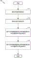
A flow diagram of an example method 900 of using a common die, such as the common die 500 illustrated in fig. 5, 8A, and 8B, or the common die 800 illustrated in fig. 10, is shown in fig. 11. In one example, method 900 is performed by a common die (such as die 500 of fig. 5) to interface with a particular selected memory type. The method 900 begins at block 910, where a memory type indication is received. In an embodiment, the memory type indication is received by DDR signal logic 520 and PHY a 531 to L542. A memory type indication may also be received by CC810 so that an appropriate clock speed may be selected. In an embodiment, the memory type indication is used to indicate whether LPDDR3 or LPDDR4 is used, and for this purpose, the memory type indication may be stored as little as 1 bit in a register (such as a CSR). The DDR signal logic 520 employs the memory type indication to route signals from the memory controller 510 to the DDR SDRAM via PHY A531 to L542 and from the DDR SDRAM to the memory controller via PHY A531 to L542. In an embodiment, DDR signaling logic 520 is configured to route CA and DQ signals according to table 1 using memory instructions.
Next, in block 920, for example, DDR signal logic 520 receives the CA signal and the DQ signal. In one embodiment, DDR signal logic 520 receives the CA signal and the DQ signal from memory controller 510. The CA signal and the DQ signal are not necessarily received at the same time, and may be separated in time by some amount. For example, for a write operation, at least one CA signal is used to provide address information to indicate where to store data in the DQ signals. Although block 920 relates to receiving one CA signal and one DQ signal, operating the memory on an ongoing basis will result in receiving multiple CA signals from the memory controller 510 and multiple DQ signals from both the memory controller 510 (e.g., for write operations) and the DQ PHY (e.g., for read operations). Further, because LPDDR3 and LPDDR4 utilize multiple DQ PHYs and multiple CA PHYs, corresponding signals for the DQ PHYs and CA PHYs are generated, which will result in multiple DQ signals and multiple CA signals. In an embodiment, additional actions are performed in which a clock signal for each of the DQ PHY and CA PHY is generated by a single clock controller (such as CC810 described earlier). In such embodiments, a clock signal is matched to each PHY.
At block 930, the CA signals are communicated or routed to a generic PHY configured as a CA PHY based on the memory type indication. In one embodiment, DDR signaling logic 520 performs this action. For example, the routing may be performed according to a table (such as table 1). For example, if LPDDR4 is being used, the memory type indication in block 910 is to indicate LPDDR4 and signal 0-CA [0] is routed to DDR PHY B532, which is configured as a CA PHY. In some embodiments, prior to block 930, an additional action is included to configure the DDR PHY B532 as a CA PHY based on the memory type indication.
Next, at block 940, DQ signals are communicated or routed to a generic PHY configured as a DQ PHY based on the memory type indication. In one embodiment, DDR signaling logic 520 performs this action. For example, the routing may be performed according to a table (such as table 1). For example, if LPDDR4 is being used, the memory type indication in block 910 is to indicate LPDDR4 and signals 0-DQ [0] are communicated to DDR PHY A531, which is configured as a DQ PHY. In some embodiments, prior to block 940, an additional action is included to configure DDR PHY a 531 as DQ PHY based on the memory type indication.
While LPDDR3 and LPDDR4 have been used in various embodiments as examples of memory types, the principles of the present disclosure may be used to modify the various embodiments of the configurable die presented herein to accommodate various other types of memory and their associated packaging and interfaces at minimal cost and packaging complexity. For example, any combination of current or future versions of LPDDR may be supported. In an embodiment, a configurable die can support a first type of memory package configuration (such as PoP) and a second type of memory package configuration (such as an external package) at minimal cost and package complexity. In an embodiment, the configurable die may be configured to support a first type of memory and a second type of memory with minimal package complexity, where the second type of memory includes a different type of interface (e.g., four or eight times the data rate) than the first type of memory.
The scope of embodiments is not limited to the specific approach shown in fig. 11. Other embodiments may add, omit, rearrange, or modify one or more actions. For example, in many real-world applications, the actions in the blocks are not performed in sequential order. For example, if the CA signal and the DQ signal in block 920 are received substantially simultaneously, the routing steps in blocks 930 and 940 may be performed substantially simultaneously. Furthermore, in some embodiments, block 910 is performed once to configure DDR signal logic 520 and a generic PHY, and then block 910 is no longer performed for a given shared die (such as shared die 500). Thereafter, block 920-.
As those of ordinary skill in the art will appreciate so far and depending on the particular application at hand, many modifications, substitutions, and variations may be made in the materials, devices, configurations, and methods of use of the apparatus of the present disclosure without departing from the spirit and scope of the present disclosure. In view of the above, the scope of the present disclosure should not be limited to the particular embodiments illustrated and described herein (as they are merely some examples of the disclosure), but rather should be fully commensurate with the appended claims and their functional equivalents.
Claims (28)
1. A configurable die, comprising:
logic elements configured to communicate control and address CA signals and data DQ signals;
a first generic physical interface (PHY) and a second generic PHY in communication with the logic element, wherein each of the first generic PHY and the second generic PHY is configurable as a CA PHY and a DQ PHY, and wherein the logic element is configurable to communicate the CA signal and the DQ signal to a different one of the first generic PHY and the second generic PHY, further wherein the first generic PHY is further configured to receive DQ signals according to a first channel, and wherein the second generic PHY is further configured to receive DQ signals according to a second channel; and
a single clock controller CC configured to provide a matched clock signal to each of the first generic PHY and the second generic PHY.
2. The configurable die of claim 1, wherein:
the logic element is further configured to:
receiving a signal conveying a value, the conveyed value being either a first value or a second value;
if the passed value is the first value:
communicate the CA signal to the first generic PHY, and
communicate the DQ signals to the second generic PHY; and
if the passed value is the second value:
communicate the CA signal to the second generic PHY, and
communicating the DQ signals to the first generic PHY.
3. The configurable die of claim 2, wherein the first value corresponds to a memory type that is low power dual data rate synchronous dynamic random access memory 3LPDDR3, and wherein the second value corresponds to a memory type that is LPDDR 4.
4. The configurable die of claim 1, further comprising:
a first plurality of generic PHYs configured as DQ PHYs, wherein the first plurality of generic PHYs are further configured to receive DQ signals according to the first channel, and wherein the second plurality of generic PHYs are further configured to receive DQ signals according to the second channel; and is
Wherein the clock controller CC is configured to provide the matched clock signal to each of the first plurality of generic PHYs and the second plurality of generic PHYs.
5. The configurable die of claim 1, wherein the configurable die further comprises a memory controller coupled to the logic element and configured to generate the CA signal and the DQ signal.
6. The configurable die of claim 5, further comprising a modem coupled to the memory controller.
7. The configurable die of claim 3, wherein the first generic PHY is configured as a DQ PHY to generate a second DQ signal to support LPDDR4 type memory.
8. The configurable die of claim 1, wherein the logic element comprises a multiplexer configured to receive the CA signal and the DQ signal and to select between the CA signal and the DQ signal to send to the first generic PHY, wherein the selection is based on a control signal input.
9. An apparatus, comprising:
a system-on-chip, SoC, for selectively supporting a first type of memory and a second type of memory, the SoC comprising:
a first generic physical interface (PHY) configurable as a Control and Address (CA) PHY and a Data (DQ) PHY in response to an input corresponding to a supported one of the first type of memory or the second type of memory;
means for communicating a CA signal and a DQ signal to the first generic PHY in response to the input,
a first plurality of generic PHYs and a second plurality of generic PHYs; and
a single clock controller CC configured to provide a matched clock signal to each of the first and second plurality of generic PHYs, wherein the first and second plurality of generic PHYs are configured as DQPHYs, wherein the first plurality of generic PHYs are further configured to receive DQ signals according to a first channel, and wherein the second plurality of generic PHYs are further configured to receive DQ signals according to a second channel.
10. The apparatus of claim 9, wherein the SoC further comprises a memory controller configured to provide the CA signals and the DQ signals.
11. The apparatus of claim 9, wherein the SoC is configured to support the first type of memory, wherein the first generic PHY is configured as a CA PHY, and wherein the means for communicating is configured to communicate only CA signals from the memory controller to the first generic PHY based on the input.
12. The apparatus of claim 9, wherein the SoC is configured to support the second type of memory, wherein the first generic PHY is configured as a DQ PHY, and wherein the means for communicating is configured to communicate only DQ signals from the memory controller to the first generic PHY based on the input.
13. The apparatus of claim 9, further comprising:
a first package configured to house the means for communicating and the first generic PHY; and
a second package comprising a memory and coupled to the first package in a package-on-package (PoP) configuration or a side-by-side package configuration.
14. The apparatus of claim 9, wherein the means for communicating is configured to receive a CA signal and a DQ signal and select between the CA signal and the DQ signal to send to the first generic PHY, wherein the selection is based on a control signal input.
15. The apparatus of claim 9, wherein the first type of memory is a low power dual data rate synchronous dynamic random access memory 3LPDDR3, and wherein the second type of memory is LPDDR 4.
16. A package on package PoP apparatus, comprising:
a first package comprising memory circuitry configured to selectively support one of a first type of memory and a second type of memory, wherein the memory circuitry comprises:
a plurality of physical interface PHYs, wherein each of the plurality of interfaces is selectively configurable as a control and address CAPHY and a data DQ PHY; and
a logic element configured to:
communicate a CA signal to a PHY of the plurality of PHYs that is configured as a CA PHY; and
communicate DQ signals to and from ones of the plurality of PHYs configured as DQ PHYs; and
a second package comprising the first type of memory or the second type of memory, wherein the second package is coupled to the first package in a PoP configuration, wherein the DQ signals and the CA signals comprise signals for a first channel and signals for a second channel, wherein the PoP apparatus further comprises a single clock controller CC configured to provide a matched clock signal to each PHY and each channel.
17. The PoP apparatus of claim 16, wherein in a first configuration:
the first type of memory is a low power dual data rate synchronous dynamic random access memory 3LPDDR 3;
the second package includes LPDDR3 memory; and is
The plurality of PHYs are configured as a first arrangement of CA PHYs and DQ PHYs compatible with LPDDR 3.
18. The PoP apparatus of claim 17, wherein in a second configuration:
the second type of memory is LPDDR 4;
the second package includes LPDDR4 memory; and is
The plurality of interfaces are configured as a second arrangement of a CA PHY and a DQ PHY compatible with LPDDR 4.
19. The PoP apparatus of claim 17, wherein the DQ signals and the CA signals comprise signals of a first LPDDR3 channel and signals of a second LPDDR3 channel.
20. The PoP apparatus of claim 16, further comprising a memory controller coupled to the memory circuitry and configured to generate the CA signal and the DQ signal.
21. The PoP apparatus of claim 20, further comprising a modem coupled to the memory controller.
22. The PoP apparatus of claim 20, wherein the logic element comprises a plurality of multiplexers, each multiplexer to select between at least two signals generated by the memory controller to select one of the signals for a corresponding PHY, and wherein the selection corresponds to a supported memory type.
23. The PoP apparatus of claim 18, wherein the second package is coupled to the first package without using an interposer.
24. A method for supporting different memory types using a single die, comprising:
receiving a memory type indication;
communicating control and address CA signals to a first generic physical interface PHY based on the memory type indication;
communicate data DQ signals to a second generic PHY based on the memory type indication; and
generating, using a single clock controller, matched clock signals for clocking the first generic PHY and the second generic PHY, wherein the CA signal and the DQ signal correspond to different channels of a memory.
25. The method of claim 24, wherein the first generic PHY is configurable as a CA PHY or a DQPHY, and wherein the second generic PHY is configurable as a CA PHY or a DQ PHY.
26. The method of claim 25, further comprising:
configuring the first generic PHY as a CA PHY based on the memory type indication; and
configuring the second generic PHY as a DQ PHY based on the memory type indication.
27. The method of claim 24, wherein the memory type indication indicates a low power dual data rate synchronous dynamic random access memory 3LPDDR3 or LPDDR 4.
28. The method of claim 24, further comprising communicating a second DQ signal from the second generic PHY to a memory controller based on the memory type indication.
Applications Claiming Priority (3)
| Application Number | Priority Date | Filing Date | Title |
|---|---|---|---|
| US14/598,528 | 2015-01-16 | ||
| US14/598,528 US9324397B1 (en) | 2015-01-16 | 2015-01-16 | Common die for supporting different external memory types with minimal packaging complexity |
| PCT/US2016/012511 WO2016114975A1 (en) | 2015-01-16 | 2016-01-07 | A common die for supporting different external memory types with minimal packaging complexity |
Publications (2)
| Publication Number | Publication Date |
|---|---|
| CN107209735A CN107209735A (en) | 2017-09-26 |
| CN107209735B true CN107209735B (en) | 2020-07-03 |
Family
ID=55272647
Family Applications (1)
| Application Number | Title | Priority Date | Filing Date |
|---|---|---|---|
| CN201680005707.9A Active CN107209735B (en) | 2015-01-16 | 2016-01-07 | Configurable die, package on package device and method |
Country Status (5)
| Country | Link |
|---|---|
| US (1) | US9324397B1 (en) |
| EP (1) | EP3245594A1 (en) |
| JP (1) | JP6710689B2 (en) |
| CN (1) | CN107209735B (en) |
| WO (1) | WO2016114975A1 (en) |
Families Citing this family (4)
| Publication number | Priority date | Publication date | Assignee | Title |
|---|---|---|---|---|
| JP6543129B2 (en) | 2015-07-29 | 2019-07-10 | ルネサスエレクトロニクス株式会社 | Electronic device |
| US11468925B2 (en) | 2018-12-03 | 2022-10-11 | Rambus Inc. | DRAM interface mode with improved channel integrity and efficiency at high signaling rates |
| US10671551B1 (en) * | 2019-02-20 | 2020-06-02 | Intel Corporation | Selective data lane interface mapping |
| US11288222B1 (en) * | 2020-09-28 | 2022-03-29 | Xilinx, Inc. | Multi-die integrated circuit with data processing engine array |
Citations (3)
| Publication number | Priority date | Publication date | Assignee | Title |
|---|---|---|---|---|
| CN101702947A (en) * | 2007-04-12 | 2010-05-05 | 拉姆伯斯公司 | Memory system with point-to-point request interconnect |
| CN102576338A (en) * | 2010-01-28 | 2012-07-11 | 惠普发展公司,有限责任合伙企业 | Interface methods and apparatus for memory devices |
| CN102929828A (en) * | 2012-10-18 | 2013-02-13 | 广东欧珀移动通信有限公司 | Data transmission method and device supporting standard and non-standard I2C (Inter-Integrated Circuit) interface simultaneously |
Family Cites Families (12)
| Publication number | Priority date | Publication date | Assignee | Title |
|---|---|---|---|---|
| US6460120B1 (en) * | 1999-08-27 | 2002-10-01 | International Business Machines Corporation | Network processor, memory organization and methods |
| US8356138B1 (en) * | 2007-08-20 | 2013-01-15 | Xilinx, Inc. | Methods for implementing programmable memory controller for distributed DRAM system-in-package (SiP) |
| WO2012064670A1 (en) * | 2010-11-09 | 2012-05-18 | Rambus Inc. | Area-efficient multi-modal signaling interface |
| US20120185663A1 (en) | 2011-01-14 | 2012-07-19 | Satoshi Yokoya | Memory Interface Converter |
| US8446903B1 (en) | 2012-05-22 | 2013-05-21 | Intel Corporation | Providing a load/store communication protocol with a low power physical unit |
| US8972640B2 (en) | 2012-06-27 | 2015-03-03 | Intel Corporation | Controlling a physical link of a first protocol using an extended capability structure of a second protocol |
| KR102004849B1 (en) | 2012-08-02 | 2019-07-29 | 삼성전자 주식회사 | Method for managing dynamic memory reallocation and device performing the same |
| US8680900B2 (en) * | 2012-08-10 | 2014-03-25 | Arm Limited | Self-initializing on-chip data processing apparatus and method of self-initializing an on-chip data processing apparatus |
| RU2633126C2 (en) | 2013-02-28 | 2017-10-11 | Интел Корпорейшн | Strengthening mechanism of transfer and/or configuration of one protocol of inter-connections for another protocol of inter-connections |
| KR102029682B1 (en) * | 2013-03-15 | 2019-10-08 | 삼성전자주식회사 | Semiconductor device and semiconductor package |
| US9123408B2 (en) * | 2013-05-24 | 2015-09-01 | Qualcomm Incorporated | Low latency synchronization scheme for mesochronous DDR system |
| US9430434B2 (en) * | 2013-09-20 | 2016-08-30 | Qualcomm Incorporated | System and method for conserving memory power using dynamic memory I/O resizing |
-
2015
- 2015-01-16 US US14/598,528 patent/US9324397B1/en active Active
-
2016
- 2016-01-07 EP EP16702240.9A patent/EP3245594A1/en not_active Withdrawn
- 2016-01-07 CN CN201680005707.9A patent/CN107209735B/en active Active
- 2016-01-07 JP JP2017537486A patent/JP6710689B2/en active Active
- 2016-01-07 WO PCT/US2016/012511 patent/WO2016114975A1/en active Application Filing
Patent Citations (3)
| Publication number | Priority date | Publication date | Assignee | Title |
|---|---|---|---|---|
| CN101702947A (en) * | 2007-04-12 | 2010-05-05 | 拉姆伯斯公司 | Memory system with point-to-point request interconnect |
| CN102576338A (en) * | 2010-01-28 | 2012-07-11 | 惠普发展公司,有限责任合伙企业 | Interface methods and apparatus for memory devices |
| CN102929828A (en) * | 2012-10-18 | 2013-02-13 | 广东欧珀移动通信有限公司 | Data transmission method and device supporting standard and non-standard I2C (Inter-Integrated Circuit) interface simultaneously |
Also Published As
| Publication number | Publication date |
|---|---|
| WO2016114975A1 (en) | 2016-07-21 |
| EP3245594A1 (en) | 2017-11-22 |
| CN107209735A (en) | 2017-09-26 |
| JP6710689B2 (en) | 2020-06-17 |
| JP2018508871A (en) | 2018-03-29 |
| US9324397B1 (en) | 2016-04-26 |
Similar Documents
| Publication | Publication Date | Title |
|---|---|---|
| US11789610B2 (en) | 3D-stacked memory with reconfigurable compute logic | |
| US9747959B2 (en) | Stacked memory devices, and memory packages and memory systems having the same | |
| EP3234784B1 (en) | Dynamic random access memory (dram) component for high-performance,high-capacity registered memory modules | |
| CN107209735B (en) | Configurable die, package on package device and method | |
| US20130194881A1 (en) | Area-efficient multi-modal signaling interface | |
| US7761668B2 (en) | Processor architecture having multi-ported memory | |
| US20110138162A1 (en) | Reconfigurable load-reduced memory buffer | |
| US9330218B1 (en) | Integrated circuits having input-output circuits with dedicated memory controller circuitry | |
| US10176138B2 (en) | Method, apparatus and system for configuring coupling with input-output contacts of an integrated circuit | |
| KR102605145B1 (en) | Semiconductor apparatus including a plurality of dies operating as a plurality of channels | |
| US9489007B2 (en) | Configurable clock interface device | |
| US11281397B2 (en) | Stacked memory device performing function-in-memory (FIM) operation and method of operating the same | |
| US8611127B1 (en) | Stacked memory device having a scalable bandwidth interface | |
| US20110018623A1 (en) | Integrated circuit package | |
| US11093434B2 (en) | Communication system and operation method | |
| KR20210143048A (en) | Memory device includng an interface circuit for data conversion in different endian formats | |
| US20140229641A1 (en) | Method and apparatus for latency reduction | |
| US8982644B1 (en) | Method and apparatus for memory control | |
| US9653132B2 (en) | Semiconductor packages usable with semiconductor chips having different pad arrangements and electronic devices having the same | |
| US20090175100A1 (en) | Method and apparatus for storage device with a logic unit and method for manufacturing same | |
| CN112041830A (en) | Communication interface and packaging structure |
Legal Events
| Date | Code | Title | Description |
|---|---|---|---|
| PB01 | Publication | ||
| PB01 | Publication | ||
| SE01 | Entry into force of request for substantive examination | ||
| SE01 | Entry into force of request for substantive examination | ||
| GR01 | Patent grant | ||
| GR01 | Patent grant |